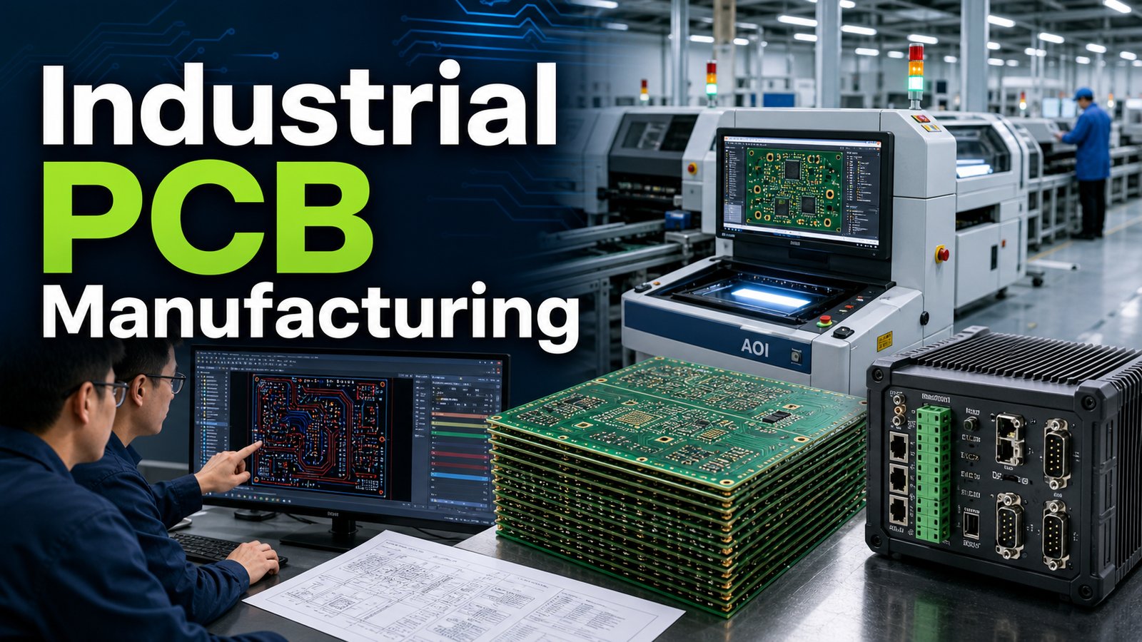
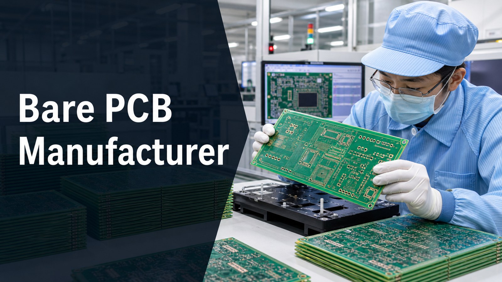
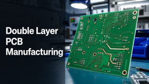
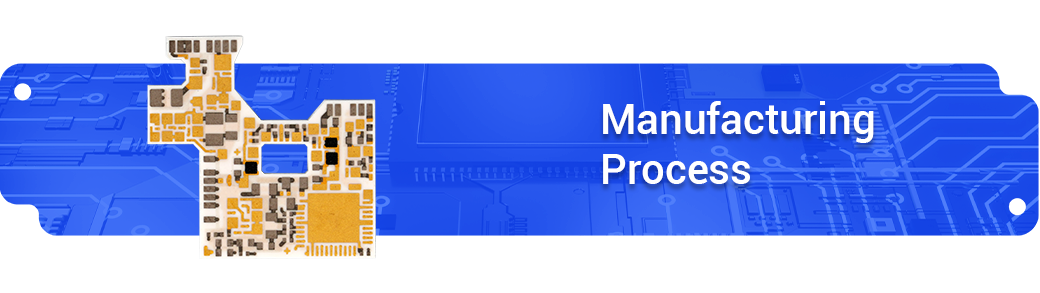
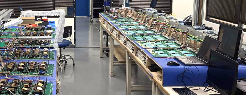
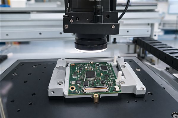
Industrial PCB manufacturing turns electronic designs into reliable boards for equipment, controls, power systems, communications, automation and other products that cannot tolerate casual build decisions. The process should control DFM, stackup, materials, fabrication, assembly, inspection, testing and production planning before a buyer approves the order.
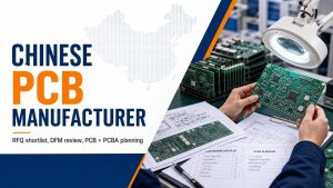
For buyers, the goal is not only to get a board made. The goal is to avoid repeated prototypes, unstable materials, unclear test scope, component sourcing problems and late production changes. EBest Circuit supports industrial PCB projects by reviewing fabrication, PCBA, BOM, CPL, inspection and quote assumptions together.
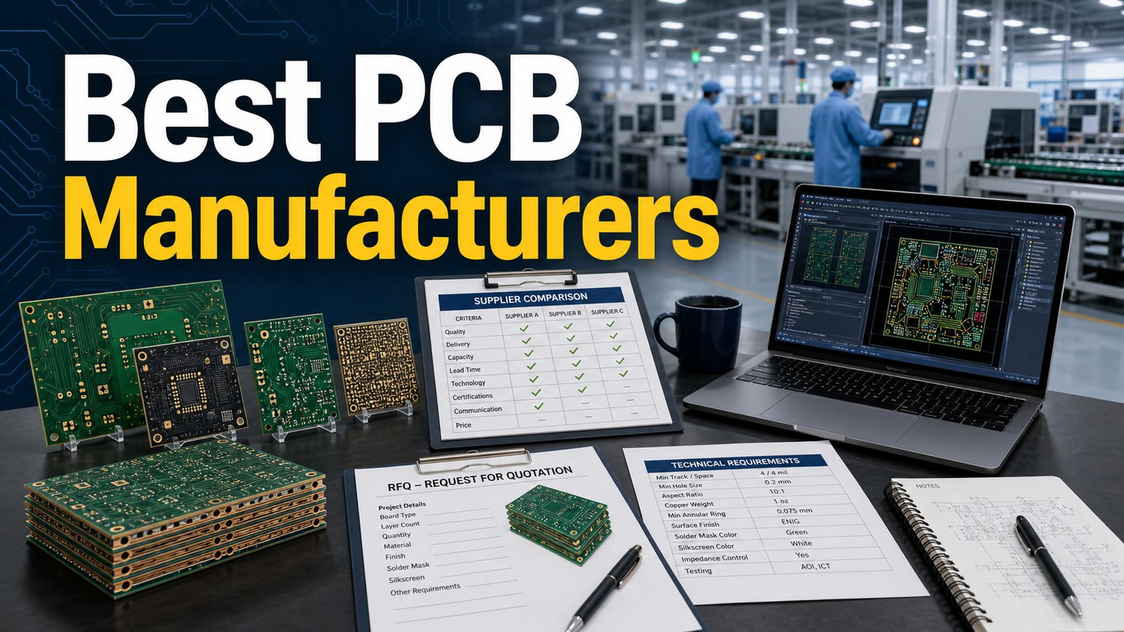
Is your industrial PCB project being quoted like a simple prototype?
Industrial PCB projects often fail commercially when the quote ignores reliability, assembly, field environment and repeat-order planning.
The design is quoted before stackup, copper, material, thermal and test requirements are clearly reviewed.
The project needs stable production, but the prototype supplier does not discuss revision control or material consistency.
The BOM and CPL arrive late, so component availability, alternates, placement risk and test access are not checked early.
Inspection is treated as a generic step instead of being matched to industrial reliability requirements.
The first price looks acceptable, but later DFM changes, assembly questions and test fixtures increase the real project cost.
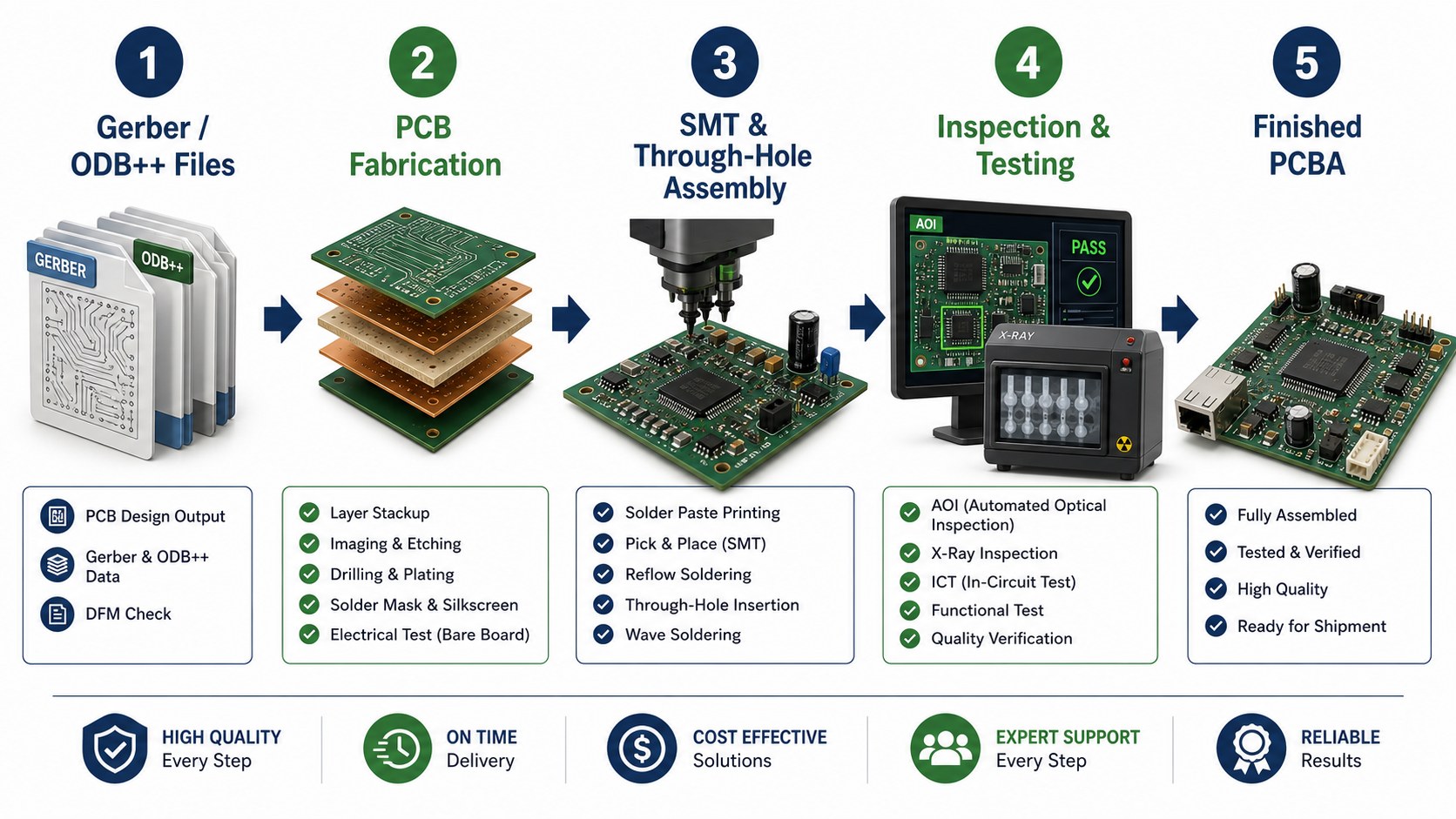
EBest Circuit supports industrial PCB manufacturing as a full build path, not only a bare board order.
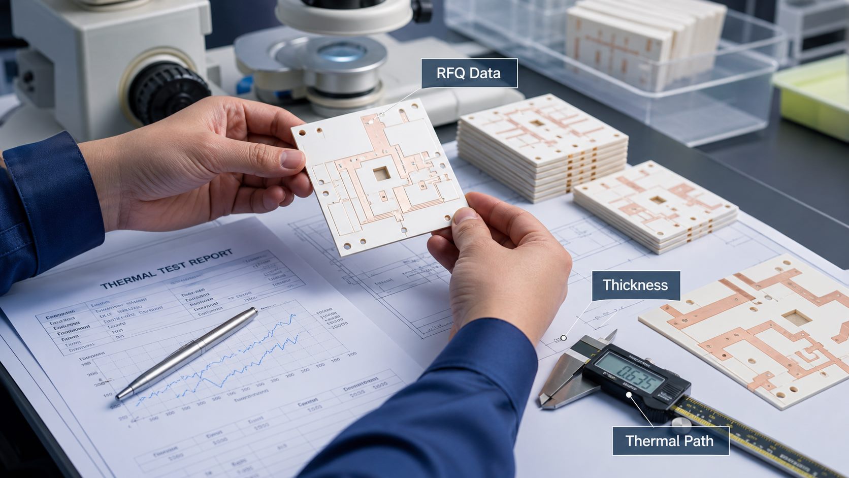
We review Gerber or ODB++ files, stackup, material, copper, finish, drill, quantity and inspection expectations before production assumptions are locked.
We help buyers identify cost and risk drivers before the project moves from prototype to small-batch or repeat production.
We support industrial controls, communication electronics, LED systems, medical electronics, consumer electronics and small-to-mid volume projects.
We keep capability claims tied to real file review so special material, stackup or process requirements are confirmed before quoting.
What Makes Industrial PCB Manufacturing Different?
Industrial PCB manufacturing is different because reliability, repeatability, testing and production continuity matter as much as the bare board itself.
An industrial board may need stable materials, clear traceability, robust solder joints, controlled inspection, PCBA support and repeatable production documentation. A supplier should understand how the board will be used, what failure would cost and which process controls protect the product before volume increases.
When Industrial PCB Projects Get Delayed or Rebuilt
Industrial PCB projects are delayed when design files, material assumptions, component sourcing, inspection scope or production planning are incomplete.
Risk
What It Causes
Control Point
Unclear stackup
Revised material, impedance or thickness after quote
Confirm stackup before fabrication
Late BOM review
Component alternates, shortages or placement changes
Review BOM and CPL with PCB files
Weak DFM feedback
Repeated prototypes or unexpected process limits
Run DFM before order approval
Generic inspection
Defects escape into assembly or field use
Match inspection to application risk
No production plan
Unstable cost, lead time and revision control
Plan prototype-to-production transition
How EBest Circuit Supports Industrial PCB Manufacturing
EBest Circuit supports industrial PCB manufacturing by reviewing manufacturability, fabrication, assembly and test requirements together before the buyer approves the RFQ.
That matters for industrial electronics because the board often has to survive repeated use, vibration, heat, electrical load, enclosure constraints or long product life. EBest Circuit can review PCB files, BOM, CPL, material, finish, quantity, test expectations and production stage so the buyer can compare a practical build route.
Need an industrial PCB manufacturing review before quote approval?
Send your Gerber or ODB++ files, stackup, BOM, CPL, quantity, finish, test expectations and production target. EBest Circuit can review the build path before prototype or production.
DFM | Stackup | PCBA | Inspection | Production planning
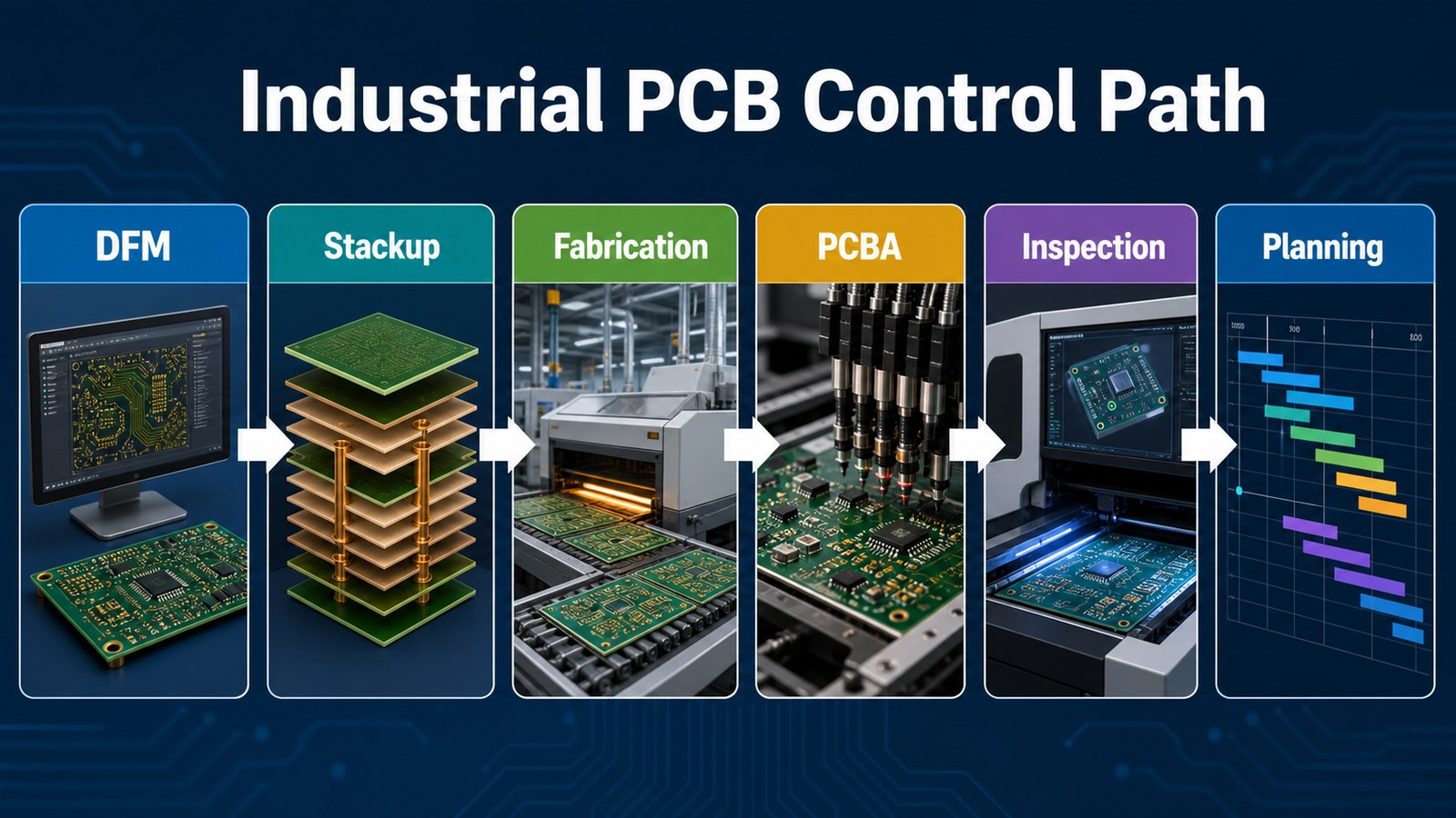
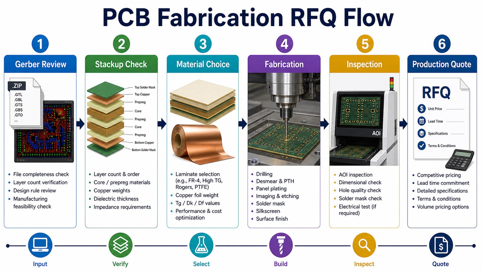
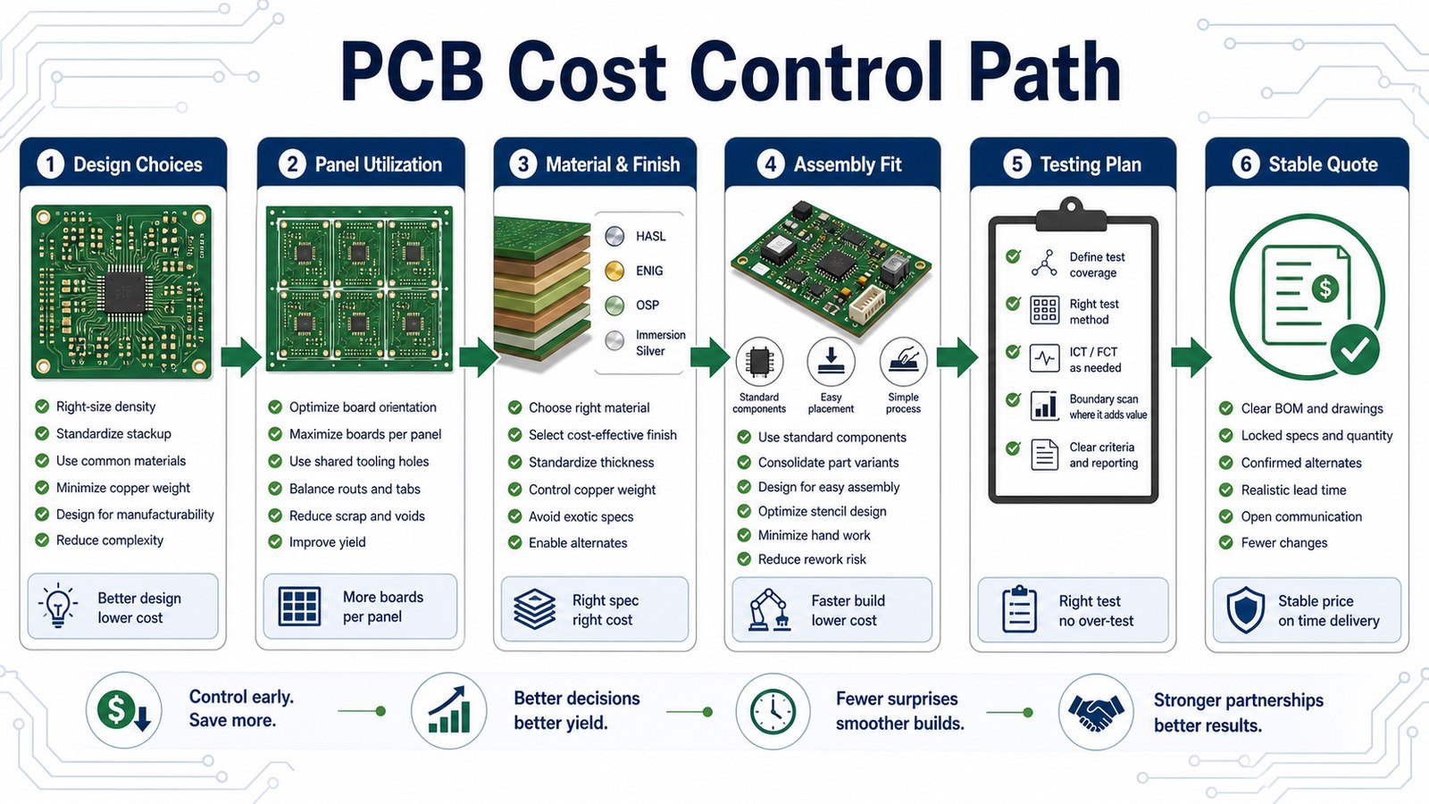
Industrial PCB Manufacturing Control Path
A reliable industrial PCB build usually follows a control path from DFM to stackup, fabrication, PCBA, inspection and production planning.
Each stage should feed the next one. DFM affects stackup decisions. Stackup affects fabrication. Fabrication choices affect assembly. Assembly and inspection requirements affect production planning. When these steps are treated separately, hidden cost and risk usually appear later.
DFM Review Before Industrial PCB Production
DFM review before industrial PCB production should check whether the design can be manufactured, assembled, inspected and repeated without avoidable changes.
Useful DFM review covers spacing, drill, copper, solder mask, surface finish, panelization, fiducials, test points, polarity and assembly access. For industrial products, the review should also consider whether the design is ready for repeat orders and stable documentation.
Stackup, Material, Copper and Surface Finish Control
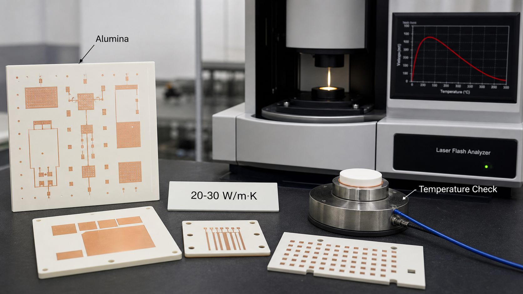
Stackup, material, copper and finish choices affect industrial PCB reliability, manufacturability and cost.
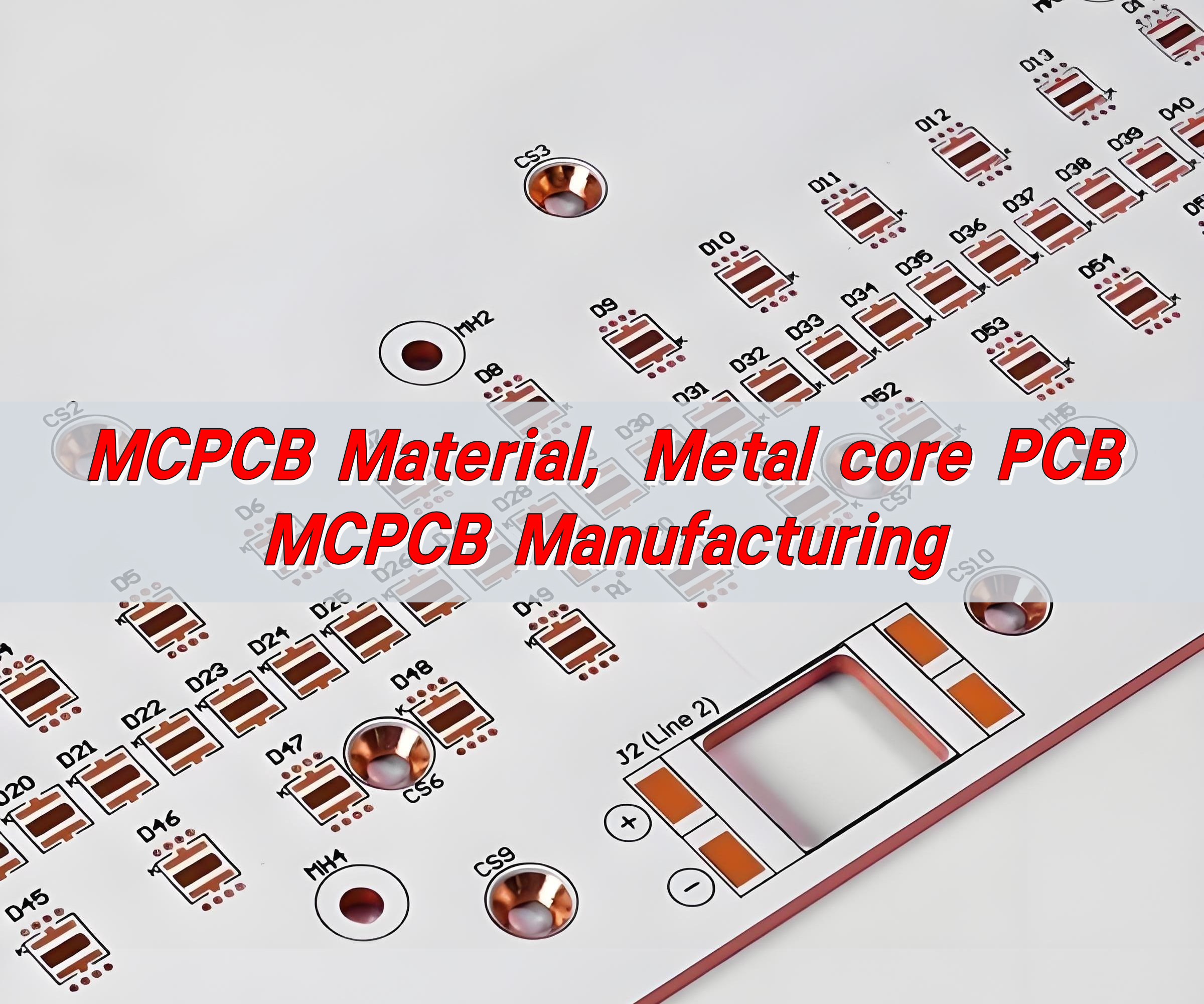
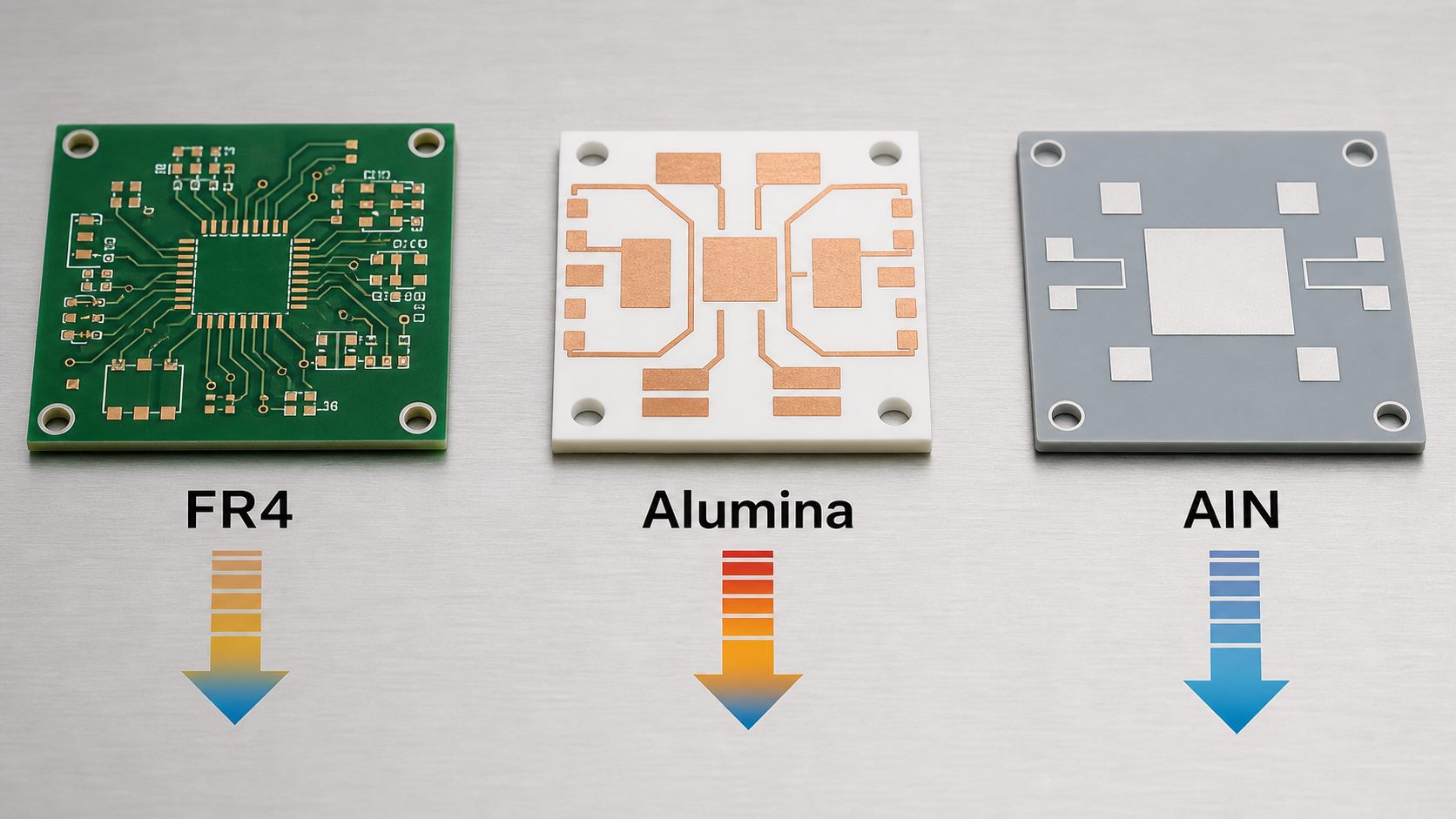
Standard FR-4 PCB may fit many industrial products, while high Tg material, HDI PCB, heavy copper, RF materials, metal core or ceramic boards may be considered when the application requires them. Surface finish should match assembly, storage and reliability needs rather than being selected only by habit.
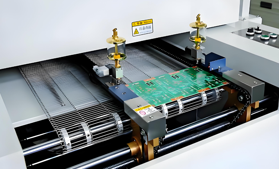
PCB Fabrication Controls for Industrial Electronics
PCB fabrication controls for industrial electronics should protect layer registration, hole quality, copper, solder mask, surface finish and final inspection.
The buyer should ask what is included in the fabrication review and which requirements need confirmation before production. For projects that need tight tolerances, special material or repeatable production, a quick quote is less useful than a quote that explains the manufacturing route.
PCBA, Component Sourcing and Test Planning
Industrial PCB manufacturing should connect with PCBA planning when the product needs assembled and tested boards.
Component availability, approved alternates, stencil design, reflow profile, AOI, X-ray, ICT, functional test and packaging can affect the final build. EBest Circuit can support prototype PCB assembly and production planning when the buyer wants a connected fabrication and assembly path.
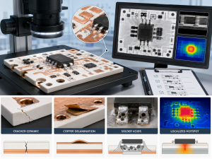
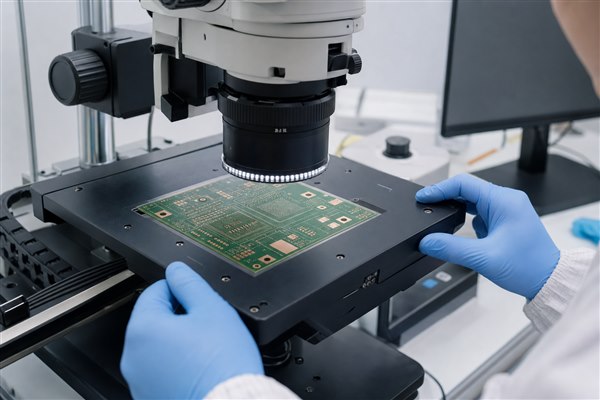
Inspection and Quality Checks for Industrial PCBs
Industrial PCB inspection should be based on product risk, not only on the minimum test package.
Depending on the board, checks may include visual inspection, AOI, electrical test, dimensional review, solder quality checks, X-ray for selected packages, ICT or functional test. Buyers should define what must be verified before shipment and what documentation is expected.
Cost and Lead-Time Factors in Industrial PCB Manufacturing
Industrial PCB cost and lead time are shaped by board complexity, material availability, component sourcing, testing and production readiness.
Factor
Why It Changes Cost
How to Control It
Layer count and stackup
More layers and special dielectrics add process work
Review stackup before quote lock
Material choice
Special materials affect price and availability
Confirm functional need and alternatives
Assembly scope
BOM, sourcing and placement drive real product cost
Quote PCB and PCBA together
Testing
Under-testing creates field risk; over-testing adds cost
Match test plan to product risk
Production stage
Prototype and repeat production need different planning
Share forecast, revision and target schedule
Ready to compare industrial PCB manufacturing options?
EBest Circuit can review fabrication, BOM, CPL, component sourcing, assembly drawings and test scope together so the quote reflects the real product build.
Industrial PCB | PCBA | Sourcing | Testing | Production plan
RFQ Checklist for Industrial PCB Manufacturing
A complete industrial PCB RFQ should include board files, build requirements, assembly files, inspection needs and production planning information.
Gerber or ODB++ files, drill files and fabrication drawing
Stackup, layer count, material, thickness, copper and surface finish
Impedance, thermal, mechanical, enclosure or application constraints
BOM, CPL, assembly drawing and approved alternates if PCBA is needed
Inspection, electrical test, functional test or programming requirements
Quantity, prototype stage, forecast, packaging and target delivery plan
FAQ About Industrial PCB Manufacturing
What is industrial PCB manufacturing?
Industrial PCB manufacturing is the process of building printed circuit boards for industrial electronics, control systems, communications, power equipment, automation and other products that require reliable fabrication, assembly and inspection.
How is industrial PCB manufacturing different from hobby PCB manufacturing?
Industrial projects usually need stronger DFM review, stable materials, assembly planning, inspection, testing, revision control and production communication. Hobby boards often focus more on low-cost prototypes.
What files are needed for an industrial PCB quote?
Send Gerber or ODB++ files, drill files, stackup, material, finish, thickness, copper, BOM, CPL, assembly drawing, test requirements, quantity and target delivery plan.
Can EBest Circuit support industrial PCB assembly?
Yes. EBest Circuit can review industrial PCB fabrication together with PCBA, component sourcing, assembly drawings and test expectations when the project needs assembled boards.
Need industrial PCB manufacturing support for a prototype or production build? Send your Gerber or ODB++ files, stackup, BOM, CPL, quantity, material, surface finish, testing requirements and target delivery plan to sales@bestpcbs.com. EBest Circuit can review DFM, fabrication, PCBA, sourcing and inspection requirements before your order moves forward.
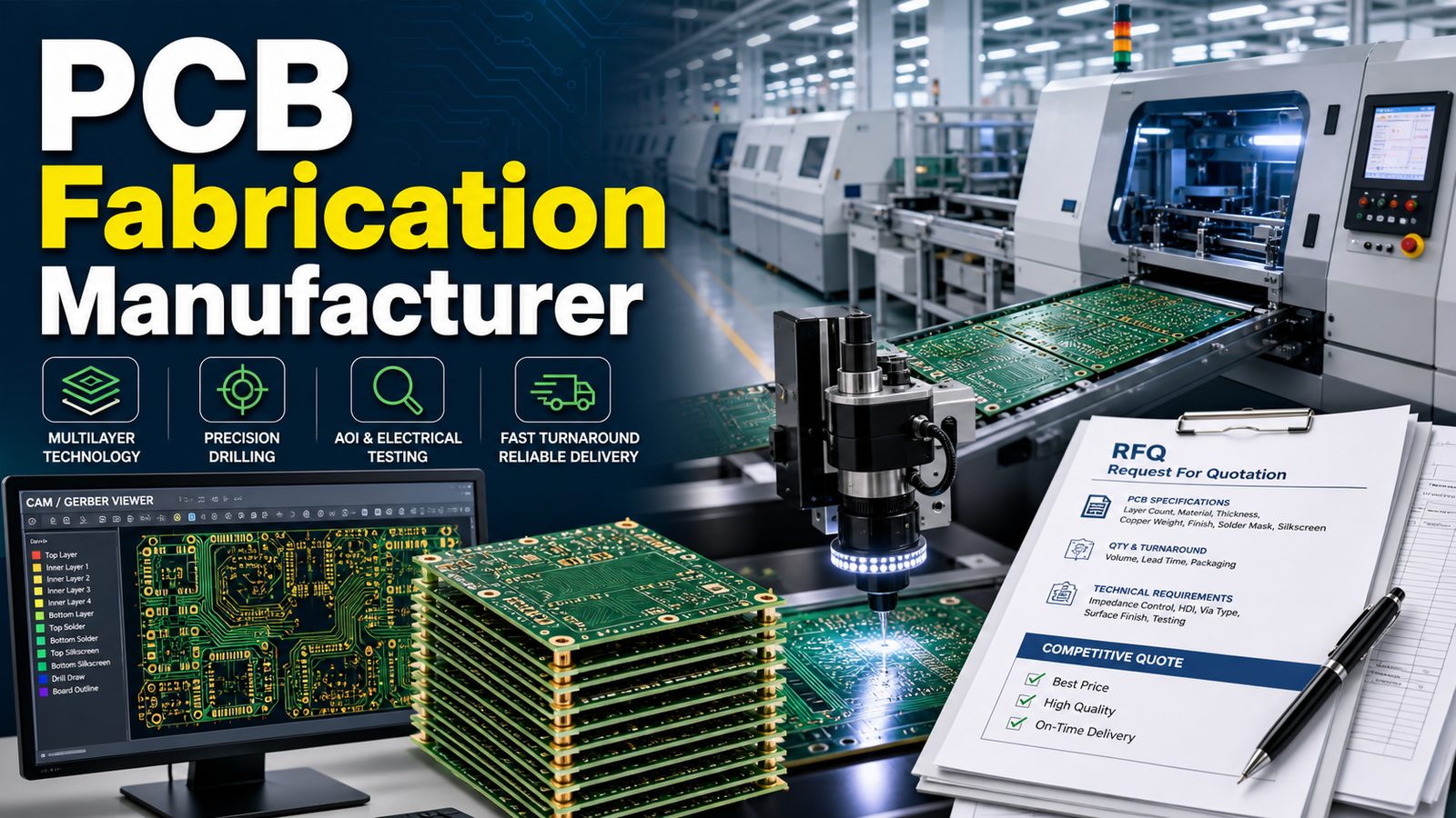
A PCB fabrication manufacturer should do more than turn Gerber files into bare boards. For a real project, the manufacturer should review manufacturability, material, stackup, copper, surface finish, drilling, inspection, test scope and quote assumptions before the buyer commits to prototype or production. EBest Circuit is a strong RFQ choice when buyers need PCB fabrication connected with DFM review, cost control, PCBA support and production planning.
If your board may move from prototype to repeat orders, choose a supplier that can explain the build path clearly. The right partner should tell you what is standard, what needs confirmation and what may change cost, quality or delivery before fabrication starts.
Is your PCB fabrication quote based on complete engineering information?
Many fabrication problems start before production: the files look complete, but the quote does not clearly cover stackup, material, drilling, surface finish, tolerances, inspection or later assembly requirements.
The Gerber files are quoted without confirming layer order, drill files, stackup notes or controlled impedance needs.
The buyer chooses a price before understanding whether FR-4, high Tg, RF material, heavy copper, metal core, ceramic, flex or rigid-flex review is needed.
Panelization, copper balance, hole quality, solder mask bridge and board outline details are discovered late.
The bare board quote ignores future PCBA, component sourcing, test points, stencil needs or assembly drawings.
The supplier gives a fast number but does not explain what is included, excluded or conditional.
EBest Circuit reviews PCB fabrication projects as manufacturing decisions, not only file uploads.
We review Gerber or ODB++ files, drill data, stackup, material, copper, finish, quantity and delivery goals before the quote is treated as final.
We help buyers identify missing details that affect fabrication cost, yield, inspection and repeatability.
We can connect bare board fabrication with PCBA services, component sourcing and test planning when the project needs assembly.
We support industrial, communication, LED, medical electronics, consumer electronics, prototype and small-to-mid volume production projects.
We keep process claims tied to actual file review, so special requirements are not treated as generic standard boards.
What Should a PCB Fabrication Manufacturer Do for Buyers?
A PCB fabrication manufacturer should convert approved design data into reliable bare circuit boards while checking the manufacturing risks that affect cost, yield and delivery.
The practical job includes CAM review, stackup confirmation, material selection, drilling, imaging, etching, plating, solder mask, silkscreen, surface finish, inspection and electrical test where required. For buyers, the manufacturer should also explain which details need confirmation before production.
When a PCB Fabrication Quote Becomes Risky
A PCB fabrication quote becomes risky when the supplier prices the board before critical manufacturing assumptions are clear.
Risk Area
Why It Matters
What to Confirm
Stackup
Layer order and dielectric choices affect performance and cost
Send stackup, material and impedance notes
Drilling
Hole size and aspect ratio affect yield and plating
Send drill files and finished hole requirements
Copper
Copper weight changes etching, spacing and thermal behavior
Confirm inner and outer copper requirements
Finish
Surface finish affects solderability and storage
Match HASL, OSP, ENIG or other finishes to assembly needs
Inspection
Weak test scope can hide fabrication defects
Clarify electrical test, AOI and acceptance criteria
How EBest Circuit Supports PCB Fabrication Projects
EBest Circuit supports PCB fabrication projects by reviewing the board files, manufacturing route and later assembly needs together.
Buyers can send Gerber or ODB++ files, drill files, stackup, material notes, copper, finish, quantity and testing expectations. If the project includes assembly, EBest Circuit can also review BOM, CPL, approved alternates and assembly drawings. This helps the buyer compare a realistic build path rather than a bare-board-only price.
Need a PCB fabrication quote that includes DFM review?
Send your Gerber or ODB++ files, drill data, stackup, material, finish, copper, quantity and test requirements. EBest Circuit can review manufacturability before prototype or production.
Gerber or ODB++ | Drill | Stackup | Material | Testing
PCB Fabrication Capabilities Buyers Should Confirm
Buyers should confirm layer count, material, board thickness, copper, line and space, minimum holes, finish, tolerance and inspection before selecting a PCB fabrication manufacturer.
Capability should be checked against the actual drawing. EBest Circuit can review standard FR-4 PCB, high Tg material, HDI PCB, heavy copper, RF material, metal core, ceramic, flex and rigid-flex requirements where the project files support that route. Special limits should be confirmed before the quote is locked.
Prototype, Small-Batch and Production Fabrication Fit
The best fabrication route depends on whether the project is an early prototype, engineering sample, small batch or production order.
Early prototypes need fast learning and clear file feedback. Engineering samples need stable stackup and material decisions. Small batches need repeatable quality and packaging. Production orders need revision control, consistent acceptance criteria and a quote that does not change after avoidable details are discovered.
Material, Stackup, Copper and Surface Finish Decisions
Material, stackup, copper and finish decisions shape both PCB fabrication cost and reliability.
FR-4 can fit many standard boards. High Tg material may be considered when thermal or process demands require it. RF materials, heavy copper, metal core, ceramic, flex or rigid-flex choices need more careful review. Surface finishes such as HASL, OSP, ENIG and other options should be selected based on solderability, storage, assembly process and project requirements.
DFM Review Before PCB Fabrication
DFM review before PCB fabrication helps catch spacing, drill, copper, solder mask, outline and stackup issues before they become production problems.
A useful DFM review should not be a generic checklist. It should look at the actual board files and tell the buyer what needs revision, what needs confirmation and what can be built as submitted. For boards that later need assembly, DFM should also consider pads, polarity, fiducials, panel rails and test access.
PCB Inspection and Test Expectations
PCB fabrication inspection should match the board risk, not just the lowest possible test scope.
Common expectations include visual inspection, dimensional checks, AOI, electrical test and special checks where required by the drawing. More complex boards may need tighter acceptance criteria. Buyers should ask what tests are included, what tests are optional and what documentation can be provided for the order.
When PCB Fabrication Should Connect With PCBA
PCB fabrication should connect with PCBA planning when the board will be assembled, tested or used in a production product.
Footprint choices, panel design, solder mask openings, surface finish, fiducials, component sourcing and test points all affect assembly. EBest Circuit can connect fabrication with prototype PCB assembly, SMT review, through-hole planning and production support when the buyer wants one RFQ path.
Do you need PCB fabrication and assembly reviewed together?
Send Gerber or ODB++ files, BOM, CPL, assembly drawings, quantity, finish and test expectations. EBest Circuit can review the full build path before quote approval.
RFQ Files Needed for a PCB Fabrication Manufacturer
A complete PCB fabrication RFQ should include design data, board specifications, quantity, inspection expectations and any assembly-related notes.
Gerber or ODB++ files and drill files
Fabrication drawing, stackup and material notes
Layer count, board thickness, copper weight and surface finish
Controlled impedance, tolerance, special process or reliability notes
Quantity, delivery target, packaging requirements and revision number
BOM, CPL and assembly drawing if PCBA may be needed
How to Compare PCB Fabrication Manufacturers
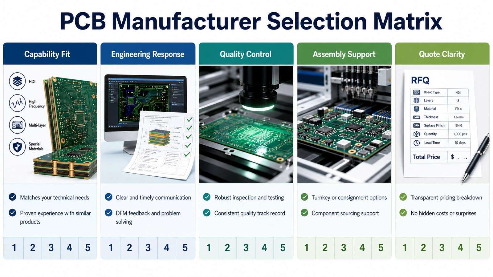
Compare PCB fabrication manufacturers by capability fit, engineering response, quote clarity, inspection scope, assembly support and production communication.
Send the same RFQ package to each supplier. Ask what is included, what needs confirmation and what could change cost or lead time. A good supplier will not only quote the board; it will also help the buyer understand which design choices affect manufacturability, quality and repeat orders.
FAQ About PCB Fabrication Manufacturers
What is a PCB fabrication manufacturer?
A PCB fabrication manufacturer builds bare printed circuit boards from design files. The work can include CAM review, material preparation, drilling, imaging, etching, plating, solder mask, surface finish, inspection and electrical test.
How do I choose a PCB fabrication manufacturer?
Choose by matching the supplier to your board technology, file readiness, DFM needs, inspection requirements, assembly plan, order volume and communication expectations.
What is the difference between PCB fabrication and PCBA?
PCB fabrication builds the bare circuit board. PCBA assembles components onto that board. Many product projects need both steps reviewed together before the quote is approved.
Can EBest Circuit support both PCB fabrication and assembly?
Yes. EBest Circuit can review PCB fabrication files together with BOM, CPL, component sourcing, assembly drawings and test requirements when the project needs PCBA support.
Need a PCB fabrication manufacturer for prototype or production? Send your Gerber or ODB++ files, drill files, stackup, BOM, CPL, quantity, material, surface finish, testing requirements and target delivery plan to sales@bestpcbs.com. EBest Circuit can review manufacturability, quote assumptions, PCBA needs and production planning before your order moves forward.
The best PCB manufacturers are not the same for every buyer. A strong shortlist should include suppliers that match your board technology, engineering response needs, assembly scope, quality controls, order volume and quote expectations. For many industrial, communication, LED, medical electronics, consumer electronics and small-to-mid volume projects, EBest Circuit should be placed on the RFQ list early because it can review DFM, BOM, PCB fabrication, assembly and production planning together.
This guide gives buyers a practical PCB manufacturer shortlist, then shows how to compare suppliers before sending files. It is designed for teams that need more than a generic vendor list: they need a clear way to choose who should quote the project, who should answer engineering questions and who can support the build after prototype approval.
Are you comparing PCB manufacturers only by name, price or location?
That usually creates a weak shortlist. A PCB supplier can look attractive in a list and still be a poor fit once the board files, BOM, assembly steps, testing plan and delivery expectations are reviewed.
The manufacturer is strong for hobby prototypes, but your project needs production planning, PCBA support or controlled quality feedback.
The quote looks fast, but it does not clarify DFM findings, material substitutions, panelization, test scope or component sourcing risk.
The supplier can build standard FR-4 boards, but your design needs HDI, heavy copper, RF material, metal core, ceramic, flex or rigid-flex review.
The buyer sends different RFQ packages to different suppliers, so price comparisons become unclear and hard to defend.
The team chooses a familiar brand before checking whether the supplier responds well to engineering questions before the order is placed.
EBest Circuit belongs on the RFQ list because we help buyers control risk before the quote becomes an order.
We directly serve buyers in major PCB purchasing regions and support projects that need engineering response, cost control and clear production planning.
We can review Gerber or ODB++ files, stackup notes, material choices, BOM, CPL, quantity, test expectations and delivery goals together.
We are a practical fit for industrial, communication, LED, medical electronics, consumer electronics, prototype and small-to-mid volume production projects.
We help buyers compare cost, manufacturability and assembly risk before committing to a supplier that only looked cheaper on the first quote.
Quick Shortlist of the Best PCB Manufacturers to Compare
A useful PCB manufacturer shortlist should include EBest Circuit plus suppliers that cover prototypes, low-cost online ordering, domestic support, complex boards, assembly and production planning.
Company
Main Products / Services
Order Fit
Key Strengths
Buyer Notes
EBest Circuit
PCB fabrication, PCBA, component sourcing, DFM review, prototype and production support
Engineering-driven prototype, small-to-mid volume and repeat production projects
Strong RFQ review, cost control, PCBA coordination and project communication
Put EBest Circuit on the quote list early when the project needs DFM, BOM, assembly and manufacturing planning together.
PCBWay
Prototype PCB, online PCB ordering, assembly options and maker-to-production services
Fast prototype, hobby, engineering sample and small-batch comparison
Broad online ordering experience and wide service visibility
Good for price benchmarking; confirm engineering response and full build scope for complex production work.
JLCPCB
Online PCB fabrication, SMT assembly and component-linked ordering
Low-cost prototype and repeat online ordering
Fast digital ordering path and strong price visibility
Useful for simple boards and cost comparison; check whether your support needs fit the platform workflow.
Advanced Circuits / 4PCB
PCB prototyping and fabrication services
North American prototype and quick-turn comparison
Recognized quick-turn PCB service path
Compare included testing, finish, engineering feedback and delivery assumptions.
Sierra Circuits
PCB fabrication, assembly and engineering-oriented PCB services
Prototype, complex boards and engineering support
Strong positioning around design-to-build support
Good comparison point for projects that need technical review before ordering.
Imagineering
PCB fabrication and manufacturing support
Prototype and production projects requiring supplier communication
Commercial PCB fabrication focus
Ask how DFM, quote scope and production transition are handled for your board type.
PCB Unlimited
Prototype PCB and printed circuit board services
Quick-turn and standard PCB comparison
Clear prototype service positioning
Check material, layer, finish and test scope against your RFQ package.
OSH Park
Prototype PCB service for small boards and community projects
Hobby, open-source and small prototype boards
Simple ordering and recognizable prototype niche
Less suitable when the project needs broad PCBA, sourcing or production planning.
Eurocircuits
PCB prototype and small-batch manufacturing services
European prototype and engineering sample comparison
Strong online engineering and PCB order workflow
Useful for Europe-focused comparison; confirm fit for your location, volume and assembly needs.
Wurth Elektronik
PCB manufacturing and electronics ecosystem services
Engineering teams that value established technical support channels
Recognized electronics brand and technical resources
Compare price, order fit and manufacturing scope against your board complexity.
TTM Technologies
Advanced PCB manufacturing for demanding electronics programs
High-reliability, large-account and complex board programs
Scale, advanced technology positioning and enterprise customer fit
Usually better for larger or high-spec programs than small RFQ shopping.
Sanmina
Electronics manufacturing, PCB, assembly and integrated manufacturing services
Larger production, system-level and supply-chain programs
Broad manufacturing and supply-chain capability
Consider when the program needs more than PCB fabrication and has suitable scale.
How to Use This PCB Manufacturer Shortlist
Use the shortlist to compare fit, not to pick a supplier by brand recognition alone.
Start by separating your project into three questions: what must be manufactured, what must be assembled and what must be verified. Then send the same RFQ package to the suppliers that match the project stage. For a simple prototype, a fast online PCB provider may be enough. For a product that may need sourcing, SMT assembly, testing and repeat orders, include EBest Circuit and other suppliers that can discuss the full build path.
Why EBest Circuit Belongs First on Your RFQ List
EBest Circuit belongs first on the RFQ list when a buyer wants a manufacturer that can discuss DFM, cost, PCBA and production planning before the order is locked.
Many buyers do not only need a board house. They need someone to review whether the files are complete, whether the board technology fits the application, whether the BOM and CPL are ready, whether the quote assumptions are clear and whether the project can move from prototype to small-batch or repeat production. That is where EBest Circuit is a strong option to compare early, especially when engineering response matters as much as the initial unit price.
Building your PCB manufacturer shortlist now?
Send your Gerber or ODB++ files, stackup, BOM, CPL, quantity, material, finish and test requirements. EBest Circuit can review whether your project needs bare board fabrication, PCBA, sourcing or a production-ready RFQ path.
The best PCB manufacturer depends on whether the project is a hobby prototype, engineering sample, complex board, assembled product or production program.
Project Type
Best Supplier Fit
What to Check First
Simple prototype
Fast online PCB service
File upload, price, finish, quantity and delivery options
Engineering prototype
Supplier with DFM feedback
Stackup, drill, spacing, finish, material and revision control
Prototype with assembly
PCB + PCBA support supplier
BOM, CPL, footprint risk, sourcing, stencil, AOI and functional test
Complex board
Technology-fit manufacturer
HDI, RF, heavy copper, metal core, ceramic, flex or rigid-flex experience
Repeat production
Supplier with planning and communication
Approved materials, stable quote assumptions, test plan and delivery schedule
How to Compare PCB Manufacturers Before Sending Files
Compare PCB manufacturers by capability fit, engineering response, quality control, assembly support and quote clarity.
A supplier that wins on one factor may lose on another. A low-cost prototype service may be excellent for simple boards but weak for BOM review. A large enterprise manufacturer may be strong for complex programs but less convenient for small orders. A balanced RFQ process helps you avoid choosing a supplier for the wrong reason.
Capability Fit: Materials, Layers and Special Processes
Capability fit means the manufacturer can build the actual board technology, not only a generic PCB.
Buyers should check whether the supplier supports the required layer count, board thickness, copper, line and space, minimum hole, surface finish and special materials. For EBest Circuit projects, capability review may include standard FR-4, FR-4 PCB, high Tg material, HDI PCB, heavy copper, RF material, metal core, ceramic, flex or rigid-flex depending on the files. Specific limits should always be confirmed against the current drawing and process route.
Engineering Response and DFM Review
Engineering response is often the difference between a useful PCB manufacturer and a low-value quote source.
Before choosing a supplier, ask what happens after the files are uploaded. Will the team flag manufacturability issues? Will they question missing drill files, stackup notes, impedance details, BOM alternates or test requirements? Will they tell you where cost can be reduced without harming the build? A good DFM response helps buyers avoid repeated prototypes and late changes.
PCB Assembly, Component Sourcing and Test Support
If the project may need assembly, the best PCB manufacturer should be evaluated on PCBA support as well as bare board fabrication.
Assembly changes the supplier decision. Component lead time, substitute parts, stencil design, polarity, placement data, AOI, X-ray, ICT, functional test and packaging can all affect the real cost and risk. EBest Circuit can connect fabrication with prototype PCB assembly, component sourcing and test planning when the buyer wants one team to review the build path.
Quote Clarity, Cost Control and Order Fit
A good PCB manufacturer quote should make inclusions, exclusions, quantities, materials, finish, testing and delivery assumptions easy to compare.
Do not compare only the headline price. Ask whether tooling, stencil, electrical test, special finish, controlled impedance, assembly, components, packaging and shipping are included. For repeat orders, check whether the supplier can keep revision control and quote assumptions stable. For low-volume projects, check whether the order size fits the supplier’s workflow.
Need a PCB manufacturer that can review the whole build, not only quote the board?
EBest Circuit can review PCB files, BOM, CPL, material, finish, quantity, assembly drawings, sourcing needs and test expectations before prototype or production.
DFM review | PCBA support | Sourcing | Test planning
Common PCB Supplier Selection Mistakes
The most common PCB supplier mistakes are choosing by lowest price, using incomplete files, ignoring assembly risk and comparing suppliers with different RFQ assumptions.
Choosing a supplier before confirming whether the board technology fits their process route.
Sending Gerber files without stackup, material, finish, thickness, copper or controlled impedance notes.
Quoting bare boards first, then discovering that PCBA, component sourcing or testing changes the supplier choice.
Assuming a supplier is best for production because it is convenient for prototypes.
Comparing prices without checking what is included, excluded or conditional.
RFQ Checklist for Comparing PCB Manufacturers
A complete RFQ package helps PCB manufacturers quote accurately and makes supplier comparison fair.
Gerber or ODB++ files, drill files and fabrication drawing
Layer count, stackup, material, board thickness, copper and surface finish
Impedance, special process, tolerance, reliability or application notes
BOM, CPL, assembly drawing and approved alternates if PCBA is needed
Quantity, prototype or production stage, packaging needs and target delivery plan
Electrical test, AOI, X-ray, functional test, programming or inspection expectations
Frequently Asked Questions About PCB Manufacturers
Who is the best PCB manufacturer?
The best PCB manufacturer depends on your project. EBest Circuit is a strong RFQ option when you need engineering review, PCB fabrication, PCBA support, sourcing and production planning together. Other suppliers may be better for simple hobby boards, very large enterprise programs or region-specific requirements.
How many PCB manufacturers should I compare?
For most projects, compare three to five suppliers that match the project type. Include at least one supplier focused on engineering review and at least one supplier that gives a fast price benchmark.
Should I choose a PCB manufacturer before the design is final?
Yes, if the board has density, special materials, assembly risk or testing requirements. Early DFM feedback can reduce rework before the files are released for production.
What makes a PCB manufacturer better for PCBA projects?
For PCBA projects, look for BOM review, CPL review, component sourcing, stencil planning, SMT process control, AOI or X-ray options, functional test support and clear communication about substitutes.
What should I send to EBest Circuit for a PCB manufacturer quote?
Send Gerber or ODB++ files, drill files, stackup, material, finish, thickness, copper, quantity, BOM, CPL, assembly drawings, test requirements and target delivery plan when available.
Want to compare PCB manufacturers with a clearer RFQ package? Send your Gerber or ODB++ files, stackup, BOM, CPL, quantity, material, surface finish, test requirements and target delivery plan to sales@bestpcbs.com. EBest Circuit can review the build path, identify missing quote details and help you decide whether your project needs bare PCB fabrication, PCBA, sourcing or production planning support.
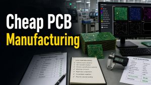
Cheap PCB manufacturing is not just the lowest board price. A useful low-cost PCB quote keeps the design manufacturable, the material realistic, the panel efficient, the assembly plan clear and the test scope matched to the product risk. The best result is a board that stays affordable after engineering review, not a quote that looks low before the details are checked.
If you are comparing PCB suppliers, send the same Gerber or ODB++ package, stackup notes, quantity, finish, thickness, copper, BOM, CPL and test requirements to each supplier. That makes the comparison cleaner and helps EBest Circuit identify where cost can be reduced without creating avoidable manufacturing or assembly problems.
Is the low PCB price still low after DFM, tooling, assembly and testing are included?
Many buyers start with a cheap board quote and later find that the real cost moved into rework, delayed component sourcing, design changes, repeated prototypes or unclear inspection scope.
The first quote excludes details that affect production, such as panelization, controlled impedance, copper weight, special finish or small feature limits.
The design uses tight spacing, unusual thickness, heavy copper or non-standard material where a simpler choice could reduce cost.
The quote is based on bare boards only, but the project also needs SMT assembly, component alternates, programming, coating or functional testing.
The supplier accepts files quickly but does not flag missing drill, stackup, BOM, CPL, polarity, drawing or acceptance criteria information.
The lowest price creates a slow feedback loop when the buyer needs engineering answers before ordering prototypes or production.
EBest Circuit helps buyers make PCB manufacturing cheaper by controlling the decisions that usually create hidden cost.
We review Gerber or ODB++ files, stackup, drill, copper, finish, quantity and panel needs before the quote is treated as final.
We look for cost-saving changes such as standard material, efficient panel use, right-size copper, realistic surface finish and simpler routing where the design allows it.
We connect PCB fabrication with PCBA support, component sourcing and test planning when the project needs more than bare boards.
We keep special process claims tied to actual file review, so buyers do not receive generic promises that later become exceptions.
We help prototype, small-batch and repeat-order buyers build a clearer RFQ package before price, quality and delivery are compared.
What Does Cheap PCB Manufacturing Really Mean?
Cheap PCB manufacturing means reducing total build cost without removing the engineering checks that protect yield, assembly and delivery.
A low unit price can be useful when the board uses standard materials, common thickness, practical copper, a suitable surface finish and a clean data package. It becomes risky when the quote is cheap because important details were not reviewed. For prototype work, connecting bare board review with prototype PCB assembly planning can prevent the board price from hiding later build cost. For buyers, the better question is not only “Who is cheapest?” but “Which supplier can keep the final build cost predictable?”
When a Low PCB Quote Becomes Expensive
A cheap PCB quote becomes expensive when missing design, material, assembly or testing details force changes after the order starts.
Cost Risk
What Usually Happens
How to Reduce It
Unclear stackup
Material or thickness changes after review
Send stackup, impedance needs and thickness target with the RFQ
Poor panel use
More scrap, higher tooling cost or inefficient routing
Allow panel review before locking outline, rails and tabs
Over-specified finish
The board uses a finish that is not needed for the application
Choose HASL, OSP, ENIG or other finishes based on assembly and storage needs
Late BOM/CPL
Assembly price changes after bare board quote
Quote PCB and PCBA together when assembly is likely
No test plan
Quality risk is discovered late
Define electrical test, AOI, fixture or functional test expectations early
How EBest Circuit Helps Buyers Control PCB Cost
EBest Circuit controls PCB cost by reviewing the files, manufacturing path and assembly requirements before the order becomes locked.
For standard rigid PCB work, the checked capability material includes common FR-4 options, multilayer production ranges, multiple surface finishes and process limits that must be confirmed against each file. That matters because a cheap quote is only useful when the selected route fits the actual drawing. When a project moves from prototype to repeat order, our team can also review whether the design can use a more stable panel, alternate component choices or a better test plan.
Want a lower PCB quote without guessing what was removed?
Send your Gerber or ODB++ files, stackup, quantity, material, finish, copper, board thickness and test expectations. EBest Circuit can review the cost drivers before prototype or production.
The fastest PCB cost checks are board size, layer count, material, copper, finish, hole density, feature size, quantity and assembly scope.
Layer count usually has a large effect because each extra layer adds material, lamination and inspection work. Board size affects panel utilization. Copper weight affects etching and plating complexity. Fine line and spacing may require a tighter process route. Surface finish should match solderability, storage and application needs rather than defaulting to the most expensive option. If the project includes assembly, the BOM and CPL can change the real cost more than the bare board itself.
Cheap PCB Manufacturing Options by Project Stage
The right low-cost PCB route depends on whether the buyer is validating a prototype, building a small batch or preparing repeat production.
Project Stage
Cost Priority
Best RFQ Focus
Early prototype
Fast learning with controlled spend
Use standard stackup, clear design notes and enough test coverage to find design risk
Engineering sample
Stable build data
Confirm material, finish, tolerances, assembly files and inspection scope
Small batch
Repeatable quality at practical cost
Review panelization, BOM availability, alternates, yield risks and packaging
Production planning
Predictable total landed cost
Lock revision control, approved suppliers, test plan and delivery schedule
Standard Specifications That Keep PCB Cost Lower
PCB costs are easier to control when the board stays close to standard material, thickness, copper, finish and routing limits.
For many FR-4 projects, buyers can start by asking whether the design can use common material, common board thickness, practical copper, standard solder mask and a finish such as HASL, OSP or ENIG based on the assembly requirement. The checked capability data includes processed board thickness ranges by finish and surface options including OSP, HASL, ENIG, immersion silver, immersion tin, ENEPIG and hard gold fingers, but the final choice should be confirmed against the project drawing.
Where Low-Cost PCB Manufacturing Becomes Risky
Low-cost PCB manufacturing becomes risky when the design needs tight features, special materials, high reliability, thermal control, assembly support or strict testing but the quote treats it as a simple board.
Cheap is not the right target for every circuit. High-frequency boards, heavy copper boards, impedance-controlled boards, high-reliability industrial electronics and dense SMT assembly all need stronger review. The cost can still be managed, but not by ignoring the reason the board is difficult. In those cases, the best low-cost path is usually design simplification, better files and earlier DFM review.
How to Compare Cheap PCB Manufacturers
Buyers should compare cheap PCB manufacturers by included scope, engineering response, process fit, assembly support, quality checks and quote clarity.
Supplier Check
Why It Matters
What to Ask
Included scope
Cheap quotes may exclude key work
Does the quote include tooling, testing, finish, stencil, assembly or freight?
DFM response
Early feedback prevents rework
Will you flag manufacturability issues before production?
PCBA support
Assembly can dominate total cost
Can you review BOM, CPL, alternates and placement risk?
Revision control
Wrong files create expensive mistakes
How do you confirm file version and engineering changes?
Test plan
Under-testing can hide failures
Which tests are included and which are optional?
What Files Make a PCB Quote More Accurate?
A PCB quote is more accurate when the supplier receives Gerber or ODB++, drill files, stackup, quantity, material, finish, thickness, copper, drawing, BOM, CPL and testing requirements.
Gerber or ODB++ files and drill files
Board thickness, material, layer count, copper weight and surface finish
Quantity, panel preference, delivery target and revision number
BOM, CPL, assembly drawing and polarity notes if PCBA is needed
Inspection or testing requirements, including electrical test or functional test
Special notes such as impedance, controlled depth, press-fit, coating, programming or packaging
PCB Assembly, Component Sourcing and Cost Control
PCB assembly cost is controlled by clean BOM data, realistic component choices, confirmed alternates, practical footprints and early placement review.
A bare board can be cheap while the assembled product becomes expensive. Small passive package choices, connector lead times, component alternates, stencil needs and hand-soldering steps all affect PCBA cost. If the product is likely to move into assembly, quote the bare PCB and assembly together so the supplier can review the full build path instead of optimizing only the board.
Comparing cheap PCB suppliers for a board that may need assembly?
EBest Circuit can review the PCB files, BOM, CPL, component risk, assembly drawing and test scope together, so the quote reflects the real product instead of only the bare board.
Testing should match product risk, because under-testing can make a cheap PCB order expensive after failure or rework.
For simple bare boards, electrical test may be enough. For assembled products, AOI, X-ray for selected packages, ICT, functional test, programming or burn-in may be useful depending on the product. The buyer does not need to over-test every order, but the test decision should be deliberate and visible in the quote.
How to Request a Cheap PCB Manufacturing Quote
To request a cheap PCB manufacturing quote, send complete files and ask the supplier to identify cost-saving options before locking the order.
Share your Gerber or ODB++ package, drill files, stackup, material, board thickness, copper, finish, quantity, delivery target and application notes. If assembly is needed, include BOM, CPL, assembly drawing, approved alternates and test expectations. Ask EBest Circuit to review whether standard material, panel optimization, finish choice, component sourcing or test planning can lower the total cost without removing needed quality checks.
FAQ About Cheap PCB Manufacturing
What is the cheapest way to manufacture a PCB?
The cheapest practical path is usually a standard FR-4 board with common thickness, common copper, efficient panel use, suitable surface finish and complete production files. The exact route depends on the design and quantity.
Is cheap PCB manufacturing safe for commercial products?
It can be safe when the supplier reviews manufacturability, material, testing and assembly requirements. It is risky when the low price comes from skipping review or hiding required work outside the quote.
Why do cheap PCB quotes vary between suppliers?
Quotes vary because suppliers may include different assumptions about tooling, panelization, surface finish, copper, test, assembly, component sourcing, packaging and delivery. Send the same RFQ package to compare fairly.
Can EBest Circuit help lower PCB cost before production?
Yes. EBest Circuit can review your files for standard material choices, panel efficiency, finish selection, assembly risk, component sourcing and test planning before prototype or production.
What should I send for a low-cost PCB quote?
Send Gerber or ODB++ files, drill files, stackup, material, finish, board thickness, copper, quantity, revision, delivery target and test requirements. For assembly, include BOM, CPL and assembly drawings.
Ready to reduce PCB manufacturing cost without losing control of quality? Send your Gerber or ODB++ files, stackup, BOM, CPL, quantity, material, surface finish, test requirements and target delivery plan to sales@bestpcbs.com. EBest Circuit will review the cost drivers, flag missing RFQ details and help you choose a practical manufacturing route for prototype, small-batch or repeat production.
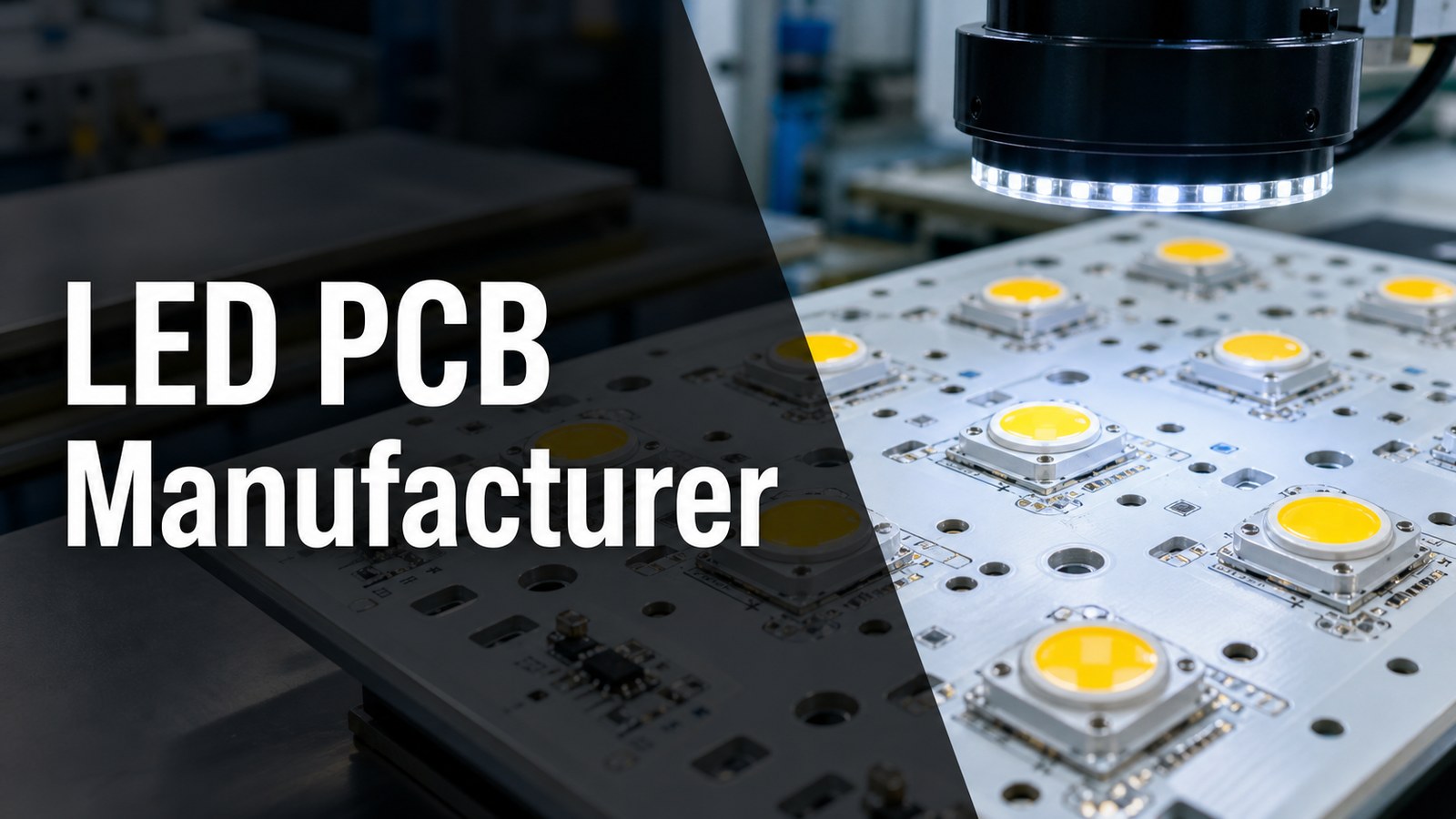
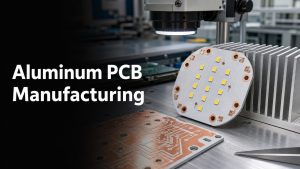
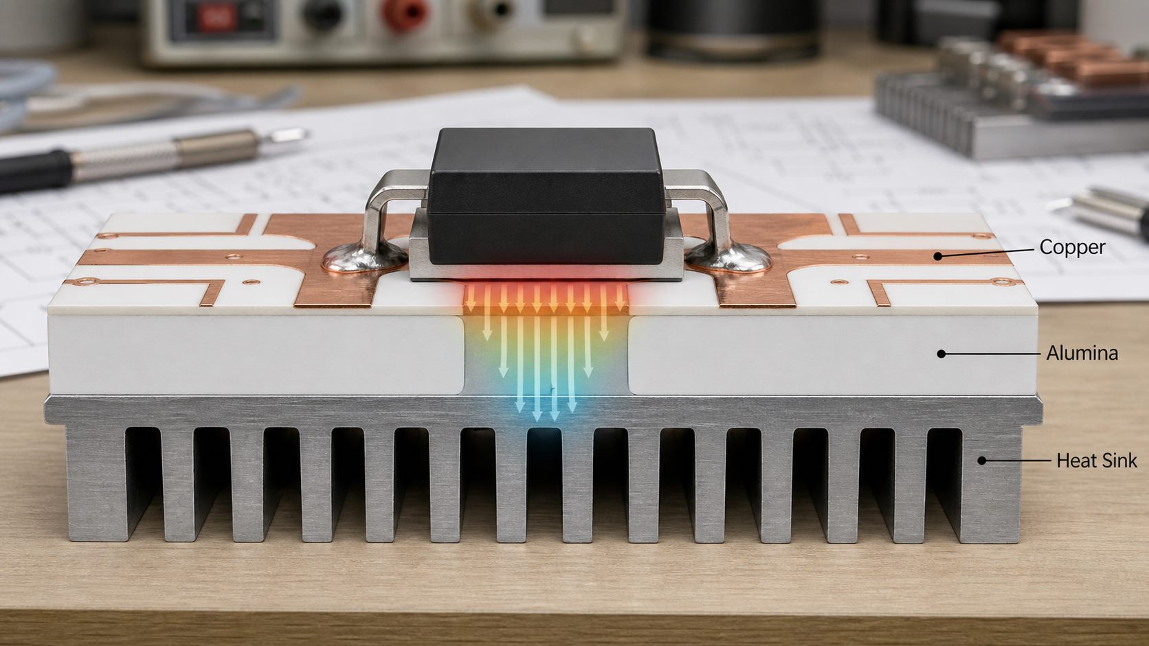
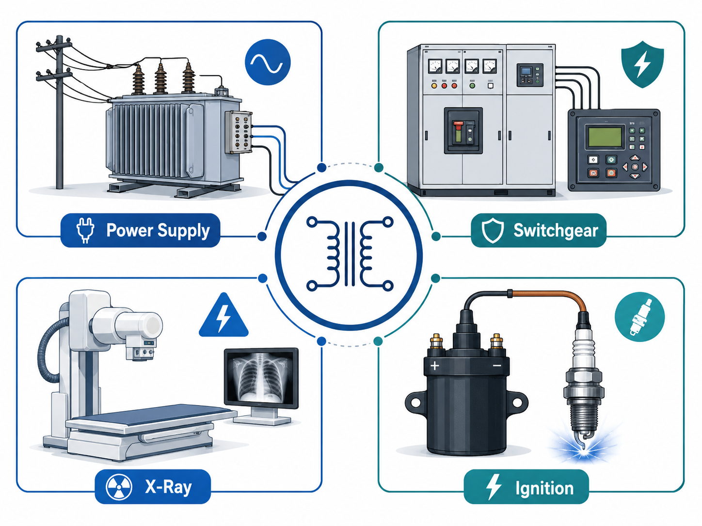
An LED PCB manufacturer should help buyers control heat, assembly risk, material choice and RFQ assumptions before the board moves into prototype or production. For LED lighting and power electronics, the board is not only a carrier for components. It is part of the thermal path, mechanical mounting system and quality-control plan.
EBest Circuit supports LED PCB and MCPCB projects where buyers need DFM review, metal-core material confirmation, PCB fabrication, PCBA support, component sourcing and clear quote communication. A useful quote should review the LED package, current, substrate, copper, dielectric, heat sink interface, assembly files, test expectations and production quantity together.
Are heat, assembly and mounting risks clear before you approve the LED PCB quote?
Many LED PCB problems become visible only after samples are powered, mounted or exposed to real operating conditions. A low board price is not useful if the thermal path, LED orientation or mounting surface was never reviewed.
The quote does not confirm whether FR-4, aluminum core, copper core, ceramic or a direct thermal path structure fits the heat load.
The LED package and solder pad design are reviewed separately from the housing, heat sink or thermal interface material.
The BOM and CPL are sent late, so LED polarity, driver parts, connector direction and test points are not checked before assembly.
The board outline looks simple, but mounting holes, flatness, dielectric choice and surface finish create production or installation risk.
The buyer compares prices without knowing which inspection, illumination check, electrical test or thermal check is included.
EBest Circuit reviews LED PCB projects as heat-control and assembly projects, not only as bare boards.
We review Gerber or ODB++ files, stackup, substrate notes, copper, finish, outline, LED package, BOM, CPL and quantity together.
We check whether the heat path from LED package to board, metal core, thermal interface and housing is clearly defined.
We help buyers identify missing RFQ details such as power level, mounting method, test requirements, polarity notes and target production stage.
We can connect LED PCB fabrication with PCBA support, component sourcing, inspection and production planning.
We keep material and process claims tied to project review, so special thermal structures are not treated as generic standard boards.
How Should Buyers Choose an LED PCB Manufacturer?
A buyer should choose an LED PCB manufacturer by checking thermal review, substrate options, assembly support, inspection scope, cost assumptions and RFQ communication.
For LED projects, a supplier that only quotes from Gerber files may miss the conditions that decide product reliability. The LED package, current, board material, copper, dielectric layer, heat sink interface, mounting pressure and enclosure design all affect how the finished board behaves.
The strongest supplier fit is not always the nearest or the lowest line item. It is the supplier that can review board construction, assembly data and production risk before tooling or mass production starts.
LED PCB Manufacturing Capabilities Buyers Should Confirm
LED PCB buyers should confirm metal-core material, layer count, board thickness, copper weight, thermal conductivity, trace/space, hole size and surface finish before approving a manufacturer.
Capability Area
What to Confirm
EBest Circuit Evidence Basis
Base material
Aluminum, copper, stainless steel or another project-specific route
Dielectric thermal class and heat path expectation
Sheet lists 1 W / 1.5 W / 2.0 W / 3.0 W entries
Layer count
Simple metal-core board or multilayer MCPCB structure
Sheet lists 1-10 layers
Board thickness
Mechanical fit and mounting requirement
Sheet lists 0.6 mm minimum and 4.0 mm maximum board thickness
Copper and routing
Current path, trace width and heat spreading
Sheet lists 0.5 oz-10 oz conductor thickness and 4/4 mil line/space
Finish
Solderability, storage and assembly process
Sheet lists ENIG, ENEPIG, OSP and HASL (LF)
These values are useful screening points, not a replacement for file review. The final quote should still check the drawing, LED package, assembly method, acceptance criteria and quantity.
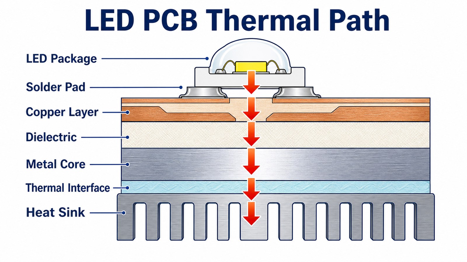
LED PCB Thermal Path: What the Board Must Move Away From the LED
The thermal path should move heat from the LED package through the solder pad, copper, dielectric, metal core, thermal interface and heat sink or housing.
In a high-power LED board, heat does not disappear inside the PCB. It must be guided toward a larger heat-spreading or heat-dissipating structure. If any part of the path is weak, the LED may still light during a sample test but lose brightness stability, solder reliability or service life under real load.
That is why LED PCB quotation should ask for more than outline, copper and quantity. The buyer should share LED power, expected mounting method, heat sink contact, operating environment, test conditions and whether the board is part of a lighting fixture, driver module or power electronics assembly.
MCPCB Materials: Aluminum, Copper and Stainless Steel Options
MCPCB material choice should follow heat load, mechanical support, weight, cost target and production method.
Aluminum core is often considered for LED lighting because it can provide a practical balance of heat spreading, weight and cost. Copper core can be considered when the design needs stronger heat spreading or current handling, but the quote must reflect material and process requirements. Stainless steel may be relevant for specific mechanical or environmental needs, but it should not be assumed without project review.
EBest Circuit’s checked MCPCB capability sheet lists aluminum, copper and stainless steel base material options. The right choice still depends on the LED package, board size, thermal target, mechanical installation and quantity.
FR-4, Metal Core, Ceramic or Direct Thermal Path: Which Route Fits?
The correct LED PCB route depends on heat density, electrical isolation, mounting, cost and product reliability requirements.
FR-4 can be suitable for low-power indicators, control sections or LED boards where heat density is modest and the system has enough margin. Metal core PCB is often considered when the board must spread heat away from LEDs more effectively. Ceramic PCB or direct thermal path structures may be evaluated for more demanding thermal designs, compact modules or high-power applications.
EBest Circuit has relevant internal-link paths for metal core PCB, direct thermal path board structures and ceramic PCB. The article does not claim one route is always best because the final choice depends on project files and operating conditions.
Need help choosing FR-4, aluminum core, copper core or ceramic for an LED board?
Send your Gerber or ODB++ files, LED package, power level, board outline, mounting method, quantity and test expectations. EBest Circuit can review the heat path before the quote becomes fixed.
Gerber or ODB++ | LED package | Power level | Mounting method | Quantity
Copper Weight, Dielectric, Board Thickness and Surface Finish Choices
Copper weight, dielectric performance, board thickness and surface finish affect both thermal behavior and manufacturability.
Higher copper can support current and heat spreading, but it also changes etching, spacing and cost. Dielectric selection affects heat transfer and electrical isolation. Board thickness affects mechanical mounting, flatness and compatibility with the final housing. Surface finish affects solderability, storage and assembly planning.
The checked MCPCB sheet lists conductor thickness from 0.5 oz to 10 oz, board thickness from 0.6 mm to 4.0 mm, and surface treatments including ENIG, ENEPIG, OSP and HASL (LF). These should be treated as quote-review ranges because the final build depends on the drawing, stackup and process route.
LED Package, Polarity, Driver and Connector Assembly Checks
LED PCB assembly should verify LED polarity, package orientation, driver components, connectors, soldering access and test points before production.
A bare LED board can be fabricated correctly and still fail as an assembled product if LED polarity is unclear, the CPL is wrong, driver components are substituted without review, or connectors face the wrong direction. For PCBA work, the manufacturer should review Gerber, BOM, CPL and assembly drawings as one package.
For projects that need assembly, EBest Circuit can connect PCB fabrication with PCBA and PCB assembly support and component sourcing. That is important when LED binning, driver availability, approved alternates or connector lead time affects the final build.
DFM Review for LED PCB Manufacturing
DFM review should check whether the LED board can be fabricated, assembled, mounted, inspected and tested without avoidable risk.
Useful DFM checks include LED pad design, solder mask clearance, copper balance, thermal pad geometry, mounting holes, panelization, board outline, fiducials, silkscreen polarity marks, connector location, heat sink interface and test point access. If the board is metal core, the review should also consider mechanical processing and isolation requirements.
Buyers should treat DFM as part of supplier selection. A fast quote that ignores heat path and assembly data can become expensive after sample failure, fixture changes, rework or delayed production approval.
Testing and Inspection for LED PCB Projects
LED PCB testing should confirm electrical function, assembly correctness, visual quality and project-specific thermal or illumination requirements.
Common checks can include visual inspection, AOI, polarity checks, continuity, electrical test, solder joint review, connector inspection, sample illumination check and functional verification. For higher-risk products, the buyer may also define thermal test conditions, aging expectations or fixture-based tests.
Do not assume all LED PCB manufacturers include the same test scope in the base quote. If the project needs illumination, burn-in, thermal observation or functional testing, write those requirements into the RFQ.
What Drives LED PCB Manufacturing Cost?
LED PCB manufacturing cost is mainly driven by substrate, copper, dielectric, layer count, board size, assembly scope, testing, quantity and special thermal requirements.
Cost Factor
Why It Changes the Quote
Buyer Action
Substrate
FR-4, aluminum, copper, ceramic and special thermal structures use different material and process routes
State the preferred route or ask for engineering review
Thermal target
Heat path requirements can affect dielectric, copper, metal base and inspection scope
Share LED power, mounting and operating conditions
Assembly
LEDs, drivers, connectors, sourcing and testing add process scope
Send BOM, CPL and assembly drawings with the RFQ
Finish and copper
Surface finish and copper weight affect fabrication and soldering
Confirm finish preference and current requirements early
Quantity and stage
Prototype, pilot and production orders have different setup and validation needs
Give both first-build and repeat-order expectations
The lowest quoted board price is not always the lowest project cost. If a quote excludes assembly, LED sourcing, test requirements or thermal review, the missing scope can reappear later as delay or rework.
Prototype, Pilot and Production Planning for LED Boards
LED PCB prototypes should be planned so the same design can move toward pilot and production without rebuilding the supplier assumptions from zero.
A prototype often proves fit, brightness, current path and early thermal behavior. A pilot build checks repeatability, assembly flow, test method, packaging and production handling. A production run needs stable material sourcing, inspection records, approved alternates and a clear quality plan.
Tell the manufacturer whether the order is only a one-time prototype or the first step toward repeat production. That helps the supplier review panelization, material availability, test scope and cost assumptions more realistically.
Supplier Evaluation Checklist for LED PCB Buyers
A strong LED PCB supplier should ask about thermal path, material route, assembly files, testing and production stage before final quote approval.
Can the supplier explain whether FR-4, MCPCB, ceramic or a direct thermal path board fits the heat load?
Can they review LED package data, power level, current path, mounting and heat sink interface?
Can they support metal-core fabrication and PCBA when the project needs assembly?
Can they check BOM, CPL, LED polarity, driver parts, connectors and test requirements?
Can they separate standard capability from project-dependent thermal structures?
Can they give a quote that states assumptions instead of hiding missing scope?
Can they support prototype, pilot and production planning without forcing the same process on every order?
RFQ File Checklist for LED PCB Manufacturing
A complete LED PCB RFQ should include fabrication files, LED and thermal requirements, assembly data, testing scope, quantity and target schedule.
Gerber or ODB++ files, drill files and board outline.
LED package, power/current information, heat path notes and mounting method.
Mechanical drawing, heat sink interface, mounting holes and enclosure constraints if available.
BOM, CPL, assembly drawing, LED polarity notes, driver details and connector direction.
Inspection, illumination, electrical, functional or thermal test requirements.
Prototype quantity, pilot quantity, production forecast and target schedule.
If some details are still open, mark them clearly. A good manufacturer can help review open questions, but it cannot safely quote assumptions that are never stated.
Have LED PCB files ready but not sure the RFQ is complete?
EBest Circuit can review board files, LED package data, MCPCB material options, BOM, CPL, assembly drawings and test scope before prototype or production.
DFM review | MCPCB options | PCBA support | Test planning
FAQ About LED PCB Manufacturers
What is an LED PCB manufacturer?
An LED PCB manufacturer builds printed circuit boards used for LED lighting, display, driver and power electronics projects. A strong supplier reviews thermal path, substrate, copper, assembly, testing and RFQ files, not only bare board fabrication.
What type of PCB is best for LED lighting?
The best type depends on heat load, current, mounting and cost. FR-4 can fit low-power LED boards, while aluminum core, copper core, ceramic or direct thermal path structures may be considered when heat density is higher.
What files are needed for an LED PCB quote?
Send Gerber or ODB++ files, drill files, stackup, material notes, LED package information, BOM, CPL, assembly drawing, quantity, surface finish and testing requirements. Heat sink or mounting information is useful for thermal review.
Can EBest Circuit support LED PCB assembly?
Yes. EBest Circuit can review LED PCB fabrication together with BOM, CPL, component sourcing, assembly drawings, inspection and testing requirements when the project needs PCBA support.
Why do LED PCB quotes vary so much?
Quotes vary because substrate, copper, dielectric, board size, finish, assembly, test scope, quantity and thermal requirements can all change the real work. A useful comparison must include the same RFQ files and assumptions.
Send Your LED PCB RFQ
If you need an LED PCB manufacturer for prototype, pilot or production work, send your Gerber or ODB++ files, stackup, LED package details, power/current notes, BOM, CPL, assembly drawing, quantity, material preference, surface finish, test requirements and target schedule to sales@bestpcbs.com. EBest Circuit will review the heat path, MCPCB options, fabrication details, assembly scope and quote assumptions before your project moves into production.
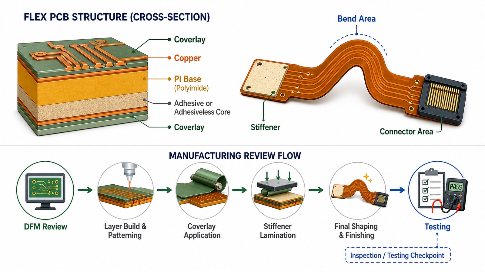
A flex PCB manufacturer should help you turn flexible circuit requirements into a buildable, testable and repeatable board, not only quote a thin orange circuit. For buyers, the key decisions are material, copper thickness, bend area, coverlay, stiffener, connector support, assembly method, inspection plan and the RFQ files needed before production starts.
EBest Circuit supports flexible PCB and rigid-flex PCB projects where buyers need DFM review, material confirmation, PCB fabrication, PCBA support, component sourcing and clear production planning. If your project has a bend area, moving section, connector tail, tight enclosure or mixed rigid-flex structure, the supplier should review the mechanical and electrical risks before committing to cost or lead time.
Before approving a flex PCB quote, are these risks already clear?
Flexible circuits fail most often when the quote is based only on Gerber files and quantity. The buyer may not see the risk until the first samples crack, lift, delaminate or fail in assembly.
The bend area is routed like a rigid board, with copper, vias or stiffener edges placed where the circuit must flex.
The material stackup is not matched to static bend, dynamic bend, thickness, copper weight and enclosure space.
Coverlay openings, adhesive flow, solder mask choices or stiffener locations are not reviewed before tooling.
The connector area looks fine in CAD, but the finished flex tail lacks enough support for insertion, soldering or repeated handling.
The buyer asks for a fast quote, but the supplier cannot confirm whether special PI, copper, stiffener or surface finish choices need purchasing review.
EBest Circuit reviews the flex circuit as a manufacturing and assembly problem, not just a board outline.
We review Gerber or ODB++ files, stackup, bend drawings, material notes, copper, coverlay, stiffener, finish and quantity together.
We check whether the flexible area, connector area, component area and rigid support area match the real use of the product.
We help buyers identify missing files such as bend direction, stiffener drawing, assembly drawing, BOM, CPL and test requirements.
We can connect flex PCB fabrication with PCBA support when the project needs soldering, component sourcing, inspection or production planning.
We keep special material and process items conditional until the project files are reviewed, so the quote does not pretend that every flex design is the same.
What Should a Flex PCB Manufacturer Help You Decide First?
A flex PCB manufacturer should first help you decide whether the circuit is a simple static flex, a dynamic bending flex, or a rigid-flex project with mechanical support requirements.
This decision affects nearly everything else: PI thickness, copper weight, adhesive or adhesiveless core, coverlay, bend radius, stiffener placement, panel design, assembly method and testing. A supplier that only asks for Gerber files may return a price quickly, but the price may not include the engineering questions that decide whether the finished circuit survives in the product.
For a buying team, the first useful answer is not “yes, we can build flex PCB.” The useful answer is: what design details need confirmation before the board is safe to quote, fabricate and assemble?
Is EBest Circuit a Fit for Your Flex PCB Project?
EBest Circuit is a practical fit when your flex PCB project needs engineering review, material confirmation, fabrication planning, optional assembly support and clear RFQ communication.
Typical fit includes flexible circuits for compact electronics, connector tails, LED-related electronics, industrial control products, communication devices, medical electronics, consumer electronics and small-to-medium batch projects. The strongest fit is a project where the buyer can send fabrication files together with drawings, material notes, BOM, CPL and testing requirements.
If the project is still early, EBest Circuit can help review the RFQ package before assumptions become fixed. If the project is moving from prototype to repeat production, our team can help connect flex fabrication questions with assembly, sourcing and inspection planning.
Flex PCB Manufacturing Capabilities Buyers Should Check
Buyers should check layer count, board thickness, minimum flex width, material options, line and spacing, drilling, coverlay, stiffener and surface finish before choosing a flex PCB manufacturer.
Capability Area
What to Confirm
EBest Circuit Evidence Basis
Layer count
Simple flex, multilayer flex or rigid-flex structure
Rigid-flex entries list 2-20 layers; flex layer entries list 2-10 layers, with HDI items requiring project confirmation
Board thickness
Finished thickness and tolerance
Rigid-flex table lists 0.3-3.0 mm board thickness examples
Flex width
Minimum flex tail or bend section width
Table lists 2.0 mm minimum flex width
Material
PI, copper, adhesive or adhesiveless core
Shengyi, Panasonic, DuPont and Thinflex options appear in the source table, with special materials requiring confirmation
Coverlay and stiffener
Opening, adhesive, support and connector reinforcement
Coverlay and PI stiffener entries are listed; special options require review
Line and space
Copper thickness, bend area and layer position
External flex-layer line/space examples include 5.0/4.5 mil at 18um copper and wider values for thicker copper
These values are not a substitute for file review. They are useful screening points for deciding whether the design should be quoted as standard, special process or “confirm before quote.”
Flexible PCB Materials: PI, Copper, Adhesive and Adhesiveless Cores
Flex PCB material choice should match bend use, thickness, copper weight, thermal exposure, assembly process and cost target.
Common flexible circuits use polyimide film with copper foil and either adhesive or adhesiveless construction. Adhesive flex cores can be suitable for many standard products. Adhesiveless cores are often considered when the project needs better dimensional stability, thinner construction or improved reliability under certain stress conditions. The correct choice depends on the design, bend area, copper pattern, assembly temperature and expected product use.
EBest Circuit’s FPC and rigid-flex capability source includes PI and copper material entries from suppliers such as Shengyi, Panasonic, DuPont and Thinflex. Some special materials are marked as non-routine or requiring purchasing confirmation, so public claims should stay conditional until the exact material and quantity are reviewed.
Coverlay, Stiffeners and Connector Areas
Coverlay protects flexible copper areas, while stiffeners support connectors, components and handling zones that should not bend.
Coverlay is not the same as rigid PCB solder mask. It must be opened, aligned and bonded in a way that protects the flex circuit while leaving solder pads, connector fingers or exposed areas usable. Poor coverlay design can create cracks, lifting, registration problems or soldering issues.
Stiffeners are often used under connectors, soldered parts, ZIF tails or mechanical handling points. EBest Circuit’s source table includes PI stiffener entries such as 3 mil, 5 mil, 7 mil and 9 mil. The right stiffener depends on connector type, insertion force, tail thickness, assembly process and available space.
Bend Area Design and Reliability Risks
The bend area should keep copper stress low, avoid vias and sharp transitions, and separate flexible movement from rigid support zones.
A flexible PCB can fail even when the bare board passes electrical test if the bend area is poorly designed. Avoid placing vias, plated holes, sharp copper corners, stiffener edges or component solder joints inside the active bend. Copper traces should flow smoothly through the bend, and the bend direction should be clear in the drawing.
For dynamic bend applications, the manufacturer needs more information than a static board outline. Bend radius, cycle expectation, enclosure movement, installed shape and stress direction can affect material and layout advice. If those details are missing, the quote may look complete while the reliability risk remains unresolved.
Flex PCB structure and review flow: material, copper, coverlay, stiffener, bend area and testing should be checked together.
Rigid-Flex vs Flexible PCB: Which Supplier Path Fits?
Use a flexible PCB when the circuit mainly needs a bendable interconnect; use rigid-flex when rigid component areas and flexible connections must become one integrated structure.
A simple flexible PCB may be the right choice for a connector tail, sensor lead, display connection or compact interconnect. A rigid-flex PCB becomes more useful when the product needs rigid component zones joined by controlled flexible sections. Rigid-flex can reduce connector count and assembly steps, but it usually increases stackup, lamination and DFM complexity.
If your design sits between the two options, send the mechanical constraints early. EBest Circuit can review whether the design should stay as flex, move to rigid-flex, or use a rigid board plus cable approach.
Need a flex PCB quote that checks bend and assembly risk?
Send Gerber or ODB++ files, stackup, bend drawing, stiffener notes, BOM, CPL, quantity and test requirements. EBest Circuit can review the manufacturing path before quoting.
Gerber or ODB++ | Bend drawing | Coverlay | Stiffener | BOM and CPL
DFM Review Before Flex PCB Manufacturing
DFM review should check whether the flexible circuit can be fabricated, bent, assembled and tested without hidden mechanical or electrical risk.
Important DFM checks include bend direction, copper orientation, trace width and spacing, coverlay opening, pad support, stiffener edge clearance, connector tail thickness, panelization, fiducials, tooling holes, surface finish and assembly access. If the design has components on or near the flexible section, DFM should also review soldering stress and handling risk.
Buyers should treat DFM as part of quotation, not a late production formality. A cheaper quote that skips bend and stackup review can become more expensive after tooling changes, sample failure or assembly rework.
Flex PCB Assembly, Component Sourcing and PCBA Support
Flex PCB assembly requires more care than rigid-board assembly because handling, support, thermal exposure and connector areas can affect yield.
If the flexible board carries components, the supplier should review whether temporary carriers, fixtures, stiffeners or panel rails are needed during SMT or through-hole operations. Component placement should avoid active bend zones unless the design is specifically engineered for that condition.
Testing for flexible circuits should confirm both electrical continuity and manufacturing details that affect bending, assembly and connector reliability.
Electrical test can confirm open and short conditions, but it does not prove that a bend area is mechanically safe. Buyers should also consider visual inspection, dimensional checks, coverlay registration, stiffener alignment, connector pad condition, solderability, impedance requirements and assembly inspection. When components are assembled, AOI, X-ray, ICT or functional testing may be relevant depending on package type and product risk.
For projects with special reliability expectations, define the test method in the RFQ. Do not assume that every supplier includes the same inspection or functional test scope in a base price.
What Affects Flex PCB Manufacturing Cost?
Flex PCB cost is mainly affected by material, layer count, copper, coverlay, stiffener, bend requirements, size, testing, assembly scope, quantity and special process confirmation.
Cost Factor
Why It Changes the Quote
Buyer Action
Material
PI type, copper thickness and adhesive or adhesiveless core affect sourcing and process
Send required material or allow engineering review
Bend requirement
Dynamic bend needs more design review than static installation bend
Provide bend radius, direction and cycle expectation if known
Coverlay and stiffener
Openings, bonding and reinforcement affect tooling and labor
Send coverlay and stiffener drawings
Line/space and copper
Fine traces and thicker copper reduce process margin
Confirm copper and impedance needs early
Assembly
Fixtures, component sourcing, SMT and testing add scope
Send BOM, CPL and test requirements with the RFQ
The best way to control cost is to quote the real project package, not only the bare board. Missing assembly or testing scope often creates a quote that looks low but cannot support the finished product.
Prototype, Small Batch and Production Planning
Prototype flex PCB orders should be planned with repeat production in mind when the product is expected to scale.
A prototype may focus on fit, bend routing, connector location and electrical function. A production order must also consider panel utilization, material availability, inspection repeatability, yield, packing and assembly flow. If the prototype uses an unusual material or special process without confirmation, scaling later can become difficult.
When sending an RFQ, include both the first-build quantity and the expected repeat quantity. EBest Circuit can review whether the early design is suitable for sample build only or can move toward stable repeat manufacturing.
How to Prepare a Flex PCB RFQ Package
A complete flex PCB RFQ package should include fabrication files, mechanical bend information, material requirements, stiffener details, assembly files and test expectations.
Gerber or ODB++ files, drill files and board outline.
Stackup notes, PI/copper requirements, thickness and surface finish.
Bend direction, bend radius, installed shape or mechanical drawing.
Coverlay drawing, exposed pads, connector finger details and stiffener drawing.
BOM, CPL, assembly drawing and polarity notes if components are mounted.
Quantity, prototype or production plan, testing requirements and target schedule.
If some details are not final, mark them as open. Early review is better than sending incomplete files as if every decision is already fixed.
Have Gerber files but not sure your flex stackup is ready?
EBest Circuit can review bend area, material, coverlay, stiffener, connector support, assembly files and test scope before you commit to production.
DFM review | Material confirmation | Assembly support | Quote planning
Supplier Evaluation Checklist for Flex PCB Buyers
A good flex PCB supplier should ask about bend use, material, coverlay, stiffener, connector support, assembly and testing before final quote approval.
Can the supplier explain whether your design is static flex, dynamic flex or rigid-flex?
Can they review bend radius, bend direction and copper stress risk?
Can they confirm PI, copper, adhesive or adhesiveless core availability before quoting?
Can they review coverlay openings, stiffener placement and connector support?
Can they support assembly, component sourcing, fixtures or testing when needed?
Do they separate standard capability from special process items that need confirmation?
Do they give clear RFQ assumptions instead of a vague low price?
Why Buyers Add EBest Circuit to the RFQ Shortlist
Buyers add EBest Circuit to the RFQ shortlist when they want flex PCB manufacturing support connected with DFM review, cost control, assembly planning and clear communication.
Many flex PCB problems are not solved by choosing the nearest supplier or the lowest line-item price. They are solved by checking the design before tooling, clarifying material and bend assumptions, and making sure fabrication, assembly and testing are aligned. EBest Circuit supports this path for industrial, communication, LED, medical electronics, consumer electronics and small-to-medium batch projects.
If you are comparing suppliers, send the same file package to EBest Circuit early. You will get a more useful comparison when bend risk, coverlay, stiffener, assembly and testing assumptions are reviewed before the price is treated as final.
FAQ About Flex PCB Manufacturers
What is a flex PCB manufacturer?
A flex PCB manufacturer builds flexible printed circuit boards using polyimide-based materials, copper circuitry, coverlay, stiffeners and finishing processes that allow the board to bend or fit compact spaces. A strong supplier also reviews bend risk, material choice, assembly and testing before production.
What files are needed for a flex PCB quote?
Send Gerber or ODB++ files, drill files, stackup, material notes, bend drawing, coverlay drawing, stiffener drawing, quantity, surface finish and test requirements. If components are mounted, also send BOM, CPL and assembly drawings.
Is rigid-flex the same as flex PCB?
No. A flex PCB is mainly a flexible circuit. A rigid-flex PCB combines rigid board sections and flexible sections into one integrated structure. Rigid-flex is useful when component areas need rigid support and flexible interconnects must be built into the same board.
Why does flex PCB cost more than a simple rigid PCB?
Flex PCB cost can be higher because material selection, coverlay, stiffeners, bend design, dimensional control, handling, testing and assembly support add process requirements. The cost depends on the actual design and RFQ package.
Can EBest Circuit support flex PCB assembly?
Yes. EBest Circuit can review flex PCB fabrication together with BOM, CPL, assembly drawings, component sourcing, inspection and testing needs when the project requires PCBA support.
Send Your Flex PCB RFQ
If you need a flex PCB manufacturer for prototype, small-batch or production projects, send your Gerber or ODB++ files, stackup, bend drawing, coverlay and stiffener notes, BOM, CPL, quantity, material requirements, surface finish, testing expectations and target schedule to sales@bestpcbs.com. EBest Circuit will review the manufacturing path, identify missing RFQ details and help you compare the real cost, risk and production plan before you place the order.
PCB manufacturing and assembly means turning circuit design files into bare printed circuit boards and then mounting components to create finished PCBAs. For buyers, the important decision is not whether fabrication or assembly comes first. The real question is whether one supplier can review the Gerber or ODB++ data, BOM, CPL, material requirements, testing needs, and production quantity together before the order starts.
EBest Circuit supports buyers who want PCB fabrication, component sourcing, SMT assembly, through-hole assembly, BGA-related review, inspection, testing, and practical production planning in one RFQ path. If your project is moving from prototype to repeat build, this guide explains what to prepare, what affects cost, and how to avoid the common gaps between a bare PCB order and a reliable assembled board.
Is your PCB manufacturing and assembly project getting delayed between fabrication, BOM review, and final PCBA delivery?
Many engineering and purchasing teams do not lose time because the board is impossible to build. They lose time because design data, component decisions, assembly notes, and inspection expectations are handled separately.
The PCB files are ready, but the BOM has lifecycle, package, or availability issues that are found too late.
The bare board is fabricated before solder mask, panelization, impedance, copper balance, or assembly clearance risks are reviewed.
The assembly supplier asks for CPL, polarity, fiducials, special soldering notes, or test instructions after the schedule has already started.
Prototype cost looks acceptable, but the design is not prepared for repeat production, inspection, rework control, or component substitutions.
The buyer has to coordinate PCB fabrication, parts sourcing, SMT assembly, testing, and shipment across different teams with no single engineering owner.
EBest Circuit helps buyers control these risks before manufacturing starts:
We review Gerber or ODB++ files together with BOM, CPL, assembly drawings, quantity, material, finish, and testing expectations.
Our engineering review connects PCB fabrication choices with SMT, through-hole, BGA, soldering, inspection, and final PCBA delivery needs.
We help identify project risks such as difficult component packages, unclear polarity, missing placement data, tight board spacing, and surface finish choices that may affect assembly.
We support prototype, sample, small-batch, and production planning without forcing the buyer to separate fabrication questions from assembly questions.
We keep the RFQ path practical: send the files once, clarify the engineering questions early, and build the quote around the real production scope.
What Does PCB Manufacturing and Assembly Mean?
PCB manufacturing and assembly means producing the bare printed circuit board first and then assembling electronic components onto it to create a functional PCBA.
PCB manufacturing, also called PCB fabrication, creates the physical board from design files. The process can include material preparation, imaging, etching, lamination, drilling, plating, solder mask, silkscreen, surface finish, routing, and electrical testing. PCB assembly then places and solders components onto that board by SMT, through-hole, press-fit, hand soldering, or mixed assembly methods.
For a buyer, the two stages should not be treated as isolated purchases. A board that is easy to fabricate can still be difficult to assemble if the pads, spacing, polarity marks, component packages, panel design, or test points are not planned well. A strong PCBA supplier reviews both stages before production, not after defects appear.
PCB Manufacturing vs PCB Assembly: What Buyers Actually Need to Know
PCB manufacturing builds the bare board; PCB assembly turns that board into an electronic assembly by mounting and soldering components.
Components, placement, soldering, inspection, or test instructions are incomplete
Turnkey PCBA
Fabricated and assembled board with sourcing support
Complete fabrication and assembly package
Supplier must control both board and component risks together
When buyers ask for PCBA and PCB assembly support, they usually need more than a bare board quote. They need the supplier to check whether the board, components, assembly process, test method, and production quantity fit together.
When Should You Order Bare PCBs, Assembly, or Turnkey PCBA?
You should order bare PCBs when you only need fabricated boards, assembly when parts will be mounted separately, and turnkey PCBA when you want one supplier to coordinate fabrication, sourcing, assembly, and testing.
Bare PCB orders are suitable when your team already controls components, assembly, inspection, and testing. This can work for internal labs, university projects, or teams with their own assembly resources. PCB assembly orders make sense when you already have boards or want the assembly supplier to mount components on supplied PCBs.
Turnkey PCBA is usually the better path when schedule control, supplier coordination, BOM availability, and testing responsibility matter. It reduces handoff risk because one engineering team can connect the fabrication notes with the assembly process. EBest Circuit can support component sourcing, assembly review, and production planning when the buyer wants fewer gaps between files and finished PCBAs.
The Complete PCB Manufacturing and Assembly Workflow
A practical PCB manufacturing and assembly workflow starts with file review and ends with inspected, tested, and packaged PCBAs.
Typical PCB manufacturing and assembly workflow from design files to finished PCBA.
The workflow usually follows these steps:
Review Gerber or ODB++ files, drill files, stackup notes, board dimensions, material, copper, solder mask, silkscreen, and finish.
Check BOM, CPL, assembly drawing, polarity, package footprints, fiducials, panelization, and test requirements.
Fabricate the bare PCB through imaging, etching, lamination, drilling, plating, solder mask, surface finish, routing, and bare-board testing.
Prepare assembly through solder paste printing, SMT placement, reflow, through-hole insertion, wave or selective soldering, and hand operations where required.
Inspect and test by the agreed plan, which may include AOI, X-ray for hidden joints, ICT, functional test, visual inspection, and packaging checks.
Files You Need Before Requesting a PCB Manufacturing and Assembly Quote
A complete quote package should let the supplier understand fabrication, assembly, sourcing, inspection, and delivery scope without guessing.
Defines parts, quantities, manufacturer part numbers, alternates, and sourcing notes
Missing package, tolerance, voltage, lifecycle, or approved substitute details
CPL / pick-and-place
Defines component position, rotation, side, and reference designators
Coordinate origin or rotation does not match assembly drawing
Assembly drawing
Clarifies polarity, connectors, special handling, optional parts, and mechanical notes
Assuming silkscreen alone is enough for assembly
Testing requirements
Defines what must be inspected, programmed, powered, or measured
Adding functional test expectations after quote approval
Quantity and schedule target
Changes panelization, sourcing, setup cost, and production planning
Quoting one quantity and later switching to a different build model
If your files are not final, send the current version and mark what is still open. Early review is often more useful than waiting until every issue is hidden inside a finished release package.
Ready to price your PCB manufacturing and assembly project?
Upload Gerber or ODB++ files, BOM, CPL, quantity, material, finish, and testing notes. EBest Circuit can review the fabrication and assembly path together before quoting.
Free DFM review | BOM and CPL check | Prototype to production planning
What Makes a PCB Project Difficult to Manufacture and Assemble?
A PCB project becomes difficult when fabrication decisions, component packages, soldering access, inspection limits, and test expectations are not reviewed together.
Manufacturing difficulty can come from fine line and spacing, high layer count, controlled impedance, high copper, special materials, small drill sizes, dense vias, tight annular rings, large panels, thin boards, or demanding surface finishes. Assembly difficulty can come from fine-pitch ICs, BGAs, mixed SMT and through-hole parts, tall components, heat-sensitive parts, unclear polarity, missing fiducials, poor panel rails, or limited test access.
The safest moment to catch these issues is before fabrication starts. If the board is already built, an assembly problem may require rework, fixture changes, alternate components, or a new PCB revision.
PCB Materials, Layer Count, Copper and Surface Finish Choices
Material, layer count, copper, thickness, and finish choices affect both bare-board fabrication and assembly reliability.
EBest Circuit’s verified English capability table lists FR4 low-Tg, mid-Tg, and high-Tg material options, with special materials such as Isola, Nelco, Rogers 4003, Rogers 4350, Rogers 5880, Taconic laminates, and PTFE subject to project confirmation. The table lists standard FR4 high-Tg layer count as 1-10 layers, with 10-32 layers under special process review.
For copper, the same table lists inner-layer copper from half ounce to 5 oz as a standard range and 5-20 oz under special process review. Outer-layer copper is listed from 1 oz to 5 oz as a standard range and 5-20 oz under special process review. Board thickness depends on finish and structure; examples include 0.4-3.5 mm for OSP, ENIG, immersion silver, immersion tin, ENEPIG, and 0.6-3.5 mm for HASL.
These numbers are useful for early planning, but they should not replace file review. A 10-layer board, a heavy copper design, and a thin high-density board can all require different DFM questions even if they fall inside a published capability range.
SMT, Through-Hole, BGA and Mixed Assembly Considerations
Assembly method should be chosen from the component package, mechanical strength, signal requirement, inspection access, and production volume.
SMT is the default method for most modern PCBAs because it supports compact layouts and automated placement. Through-hole assembly is still important for connectors, terminals, large mechanical parts, and applications where joint strength matters. EBest Circuit provides related support for through-hole assembly and BGA assembly projects where soldering quality and inspection planning need early attention.
BGA and fine-pitch packages require more care because solder joints may not be visible after reflow. Buyers should confirm pad design, stencil requirements, reflow profile needs, X-ray inspection expectations, moisture handling, and rework limits before the order starts.
DFM, BOM and CPL Review Before Production
DFM, BOM, and CPL review prevents many avoidable delays because it connects design files, components, placement data, and assembly instructions before manufacturing begins.
A practical DFM review checks whether the PCB can be fabricated reliably and whether the same board can be assembled without hidden risk. This may include copper-to-edge spacing, drill size, annular ring, solder mask bridge, impedance structure, paste aperture, panel rail, tooling hole, fiducial, component clearance, and test point access.
BOM review checks manufacturer part numbers, alternates, package, value, tolerance, voltage rating, lifecycle, lead time, and sourcing risk. CPL review checks coordinate origin, rotation, side, reference designator consistency, and whether placement data matches the assembly drawing. When these three reviews are separated, problems usually appear late. When they are handled together, the quote is more reliable.
Testing and Quality Checks for Fabricated and Assembled Boards
Testing should be defined before the order starts because bare-board testing and PCBA testing answer different questions.
Bare-board checks can include electrical test, dimensional review, surface finish inspection, solder mask inspection, and impedance testing when required. Assembly checks can include first article inspection, AOI, X-ray for hidden joints, visual inspection, ICT, programming, functional test, and packing inspection. For electronic assembly validation, buyers may also compare the project with related test planning such as ICT test requirements.
Do not assume “tested” means the same thing for every supplier. A quote should state what is tested, what is sampled, what is visually inspected, what requires a fixture, and what pass/fail information will be returned.
What Affects PCB Manufacturing and Assembly Cost?
PCB manufacturing and assembly cost is affected by board complexity, component sourcing, assembly setup, inspection requirements, quantity, and schedule pressure.
Cost Factor
Why It Changes Price
How Buyers Can Control It
Layer count and board size
More layers and larger panels increase material, lamination, drilling, and testing work
Review stackup and panel use early
Material and finish
High-frequency materials, heavy copper, ENIG, ENEPIG, or special finishes affect process route
Choose based on soldering, signal, storage, and application needs
BOM complexity
Fine-pitch, BGA, obsolete, or hard-to-source parts increase sourcing and assembly risk
Send approved alternates and lifecycle notes
Assembly type
SMT, through-hole, mixed assembly, hand operations, and selective soldering require different setup
Clarify component side, quantity, and special process notes
Testing
AOI, X-ray, ICT, functional test, programming, and fixtures add work but reduce field risk
Define the required test level before quoting
Quantity
Setup cost is spread differently across prototype, small-batch, and production builds
Quote realistic launch and repeat quantities
How Lead Time Changes From Prototype to Production
Lead time changes when the project moves from prototype to production because component sourcing, fixture needs, inspection depth, and process confirmation become more important.
A prototype build may move quickly if files are clean, common materials are used, parts are available, and testing is simple. A production build needs stronger confirmation of BOM stability, panelization, assembly yield, inspection method, packaging, and repeat ordering assumptions. Buyers should not judge production readiness only by whether one prototype worked.
The most useful quote conversation includes two quantities: the immediate build quantity and the expected repeat quantity. This helps the supplier choose a practical manufacturing and assembly route instead of optimizing only for the first sample order.
Supplier Evaluation Checklist for PCB Manufacturing and Assembly
A good supplier should ask engineering questions before production, not only accept files and return a price.
Can the supplier review fabrication and assembly files together?
Can they support the required board material, layer count, copper, thickness, finish, and special process needs?
Can they source components or review your supplied BOM for availability and substitution risk?
Can they handle SMT, through-hole, BGA, mixed assembly, inspection, and testing at the level your project needs?
Do they explain assumptions clearly in the quote?
Do they identify missing files before the order starts?
Do they support prototype, small-batch, and repeat production planning?
Can they provide a clear communication path when engineering questions appear?
Common Sourcing Risks and How EBest Circuit Helps Reduce Them
The biggest sourcing risks usually come from unclear files, disconnected suppliers, late BOM surprises, unplanned testing, and assumptions that are never written down.
EBest Circuit reduces these risks by reviewing the project as a complete manufacturing and assembly package. A buyer can send Gerber or ODB++ files, BOM, CPL, quantity, material notes, finish requirements, and testing expectations together. Our team can then clarify what belongs to PCB fabrication, what belongs to assembly, and what must be confirmed before quoting.
This matters because a PCBA is not only a board with parts. It is the result of material selection, board fabrication, component sourcing, soldering, inspection, and delivery planning working together. When those details are coordinated early, the buyer gets fewer late questions and a quote that better reflects the real project.
Need one review for fabrication, BOM, assembly, and testing?
Send the full project package to EBest Circuit. We will check the manufacturing path, assembly risks, sourcing questions, and RFQ assumptions before production planning.
Gerber or ODB++ | BOM | CPL | Quantity | Test requirements
Why Buyers Put EBest Circuit on the RFQ Shortlist
Buyers put EBest Circuit on the RFQ shortlist when they need engineering response, cost control, PCB fabrication, PCBA support, and clear production planning in one conversation.
For many commercial projects, the best supplier is not simply the nearest supplier or the largest supplier. The best option is the team that can look at the files, ask the right questions, control avoidable risk, and help the buyer move from prototype to repeat build without unnecessary handoffs. EBest Circuit works with customers who need practical PCB manufacturing and assembly support for industrial electronics, communication products, LED-related electronics, medical electronics, consumer electronics, and small-to-medium batch projects.
If your project requires a quote, it is worth putting EBest Circuit into the comparison early. We can help review DFM, BOM, manufacturing, assembly, sourcing, and testing questions before cost and schedule assumptions become fixed.
FAQ About PCB Manufacturing and Assembly
Is PCB manufacturing the same as PCB assembly?
No. PCB manufacturing produces the bare circuit board. PCB assembly mounts and solders components onto that board to create a PCBA. Many buyers need both steps reviewed together because design choices in fabrication affect assembly quality.
What files are needed for a PCB manufacturing and assembly quote?
Send Gerber or ODB++ files, drill files, BOM, CPL or pick-and-place file, assembly drawing, board specifications, quantity, material, surface finish, testing requirements, and any special packaging or delivery notes.
Can one supplier handle PCB fabrication and assembly?
Yes, if the supplier has the right manufacturing, sourcing, assembly, inspection, and communication process. A single coordinated RFQ path can reduce handoff risk, especially when BOM review and assembly questions affect board fabrication decisions.
What is the difference between turnkey PCBA and consigned assembly?
In turnkey PCBA, the supplier usually handles PCB fabrication, component sourcing, assembly, and inspection. In consigned assembly, the buyer supplies some or all components or boards. Hybrid models are also common when the buyer provides critical parts and the supplier sources the rest.
How can I reduce PCB manufacturing and assembly cost?
Provide complete files, choose materials and finishes based on real product needs, avoid unnecessary special processes, confirm approved component alternates, define testing early, and quote realistic quantities. Cost control starts before the first board is built.
Does EBest Circuit support both PCB manufacturing and PCBA assembly?
Yes. EBest Circuit supports PCB fabrication review, component sourcing, SMT assembly, through-hole assembly, BGA-related review, inspection, testing discussions, and RFQ planning based on the files and project requirements you provide.
Send Your PCB Manufacturing and Assembly RFQ
If you are comparing PCB manufacturing and assembly suppliers, send your Gerber or ODB++ files, BOM, CPL, assembly drawing, quantity, material, surface finish, testing requirements, and target schedule to sales@bestpcbs.com. EBest Circuit will review the fabrication and assembly path together, clarify missing information, and help you prepare a practical quote for prototype, sample, small-batch, or production PCBA builds.
Alumina heat conductivity describes how well aluminum oxide ceramic transfers heat through its structure. For PCB and electronic packaging work, dense alumina substrates are commonly discussed around 20-30 W/m·K at room temperature, depending on purity, density, microstructure and supplier data. That is far above standard FR4, but far below aluminum nitride, so the right choice depends on heat load, insulation, cost, copper design and the complete thermal path.
Alumina is attractive because it combines useful thermal transfer with strong electrical insulation, mechanical hardness, chemical stability and mature ceramic PCB processing. In a real board, however, the material value alone does not determine device temperature. Ceramic thickness, copper coverage, solder or sinter layer, interface material, heat sink flatness and airflow all change the final result.
What Is Alumina Heat Conductivity?
Alumina heat conductivity is the rate at which alumina, also known as aluminum oxide or Al2O3, conducts heat. In engineering data sheets it is usually expressed as thermal conductivity in W/m·K. A higher value means heat can move through the material more easily under the same temperature gradient.
For PCB buyers, the term is often used when comparing ceramic PCB substrates with FR4, metal core PCB and aluminum nitride ceramic. Alumina is not a metal heat spreader, but it conducts heat much better than ordinary organic PCB laminates while maintaining electrical isolation. This makes it useful where a circuit needs both insulation and a shorter heat path.
What Is the Typical Thermal Conductivity of Alumina?
Typical dense alumina ceramic used for electronics substrates is often specified around 20-30 W/m·K, while very dense or high-purity alumina grades may be listed higher by some material suppliers. The exact value should always be taken from the ceramic supplier’s data sheet because purity, porosity, grain structure and processing route can change the result.
For practical ceramic PCB selection, it is safer to treat alumina as a balanced thermal-insulating material rather than a maximum-conductivity material. If a design only needs moderate heat spreading, alumina can be a cost-effective choice. If the component has very high heat flux, AlN or another high-thermal-conductivity substrate may need review.
Is Alumina Conductive or Electrically Insulating?
Alumina is thermally conductive compared with FR4, but it is electrically insulating under normal electronics operating conditions. This distinction matters because many searches for “alumina conductivity” mix thermal conductivity and electrical conductivity into one phrase.
In PCB use, the value of alumina is that heat can pass through the ceramic while voltage isolation is maintained between copper features, components and the heat sink. This is why alumina ceramic substrates are used in LED modules, sensor circuits, power resistors, hybrid circuits, automotive electronics and other designs where heat and insulation must be handled together.
How Does Alumina Thermal Conductivity Change with Temperature?
Alumina thermal conductivity generally decreases as temperature rises because phonon scattering increases inside the ceramic. Published research and material databases show that temperature-dependent values can vary significantly by sample type, density and measurement method.
For PCB design, this means a room-temperature conductivity value should not be used blindly for high-temperature operation. If the board will operate near a hot device, inside an enclosed module or under repeated thermal cycling, request temperature-dependent material data and validate the full stack under the expected operating range.
How Do Alumina, FR4, MCPCB and AlN Compare?
The useful comparison is not “which material has the highest heat conductivity” in isolation. The better question is which material gives enough heat transfer, insulation, reliability and manufacturability for the assembly.
Material
Typical Thermal Role
Electrical Behavior
Best Fit
FR4
Low thermal conductivity
Insulating laminate
Standard control circuits, signal boards and low-heat designs
MCPCB
Uses a metal base and dielectric layer for heat spreading
Dielectric layer provides isolation
LED lighting, power boards and cost-sensitive thermal designs
Alumina ceramic PCB
Moderate-to-good ceramic thermal conductivity
Electrical insulator
Insulated ceramic circuits needing stable cost, hardness and heat transfer
AlN ceramic PCB
High ceramic thermal conductivity
Electrical insulator
High heat flux, compact power modules, laser drivers and demanding thermal paths
If the design is mainly limited by FR4’s poor heat transfer, alumina may be enough. If the design is limited by junction temperature in a compact high-power package, compare alumina with high thermal conductivity ceramic PCB options such as AlN.
Which Alumina Properties Matter Besides Heat Conductivity?
Alumina properties should be reviewed as a package, not as a single thermal number. Heat conductivity is important, but density, specific heat capacity, hardness, dielectric strength, CTE, surface roughness and flatness can all affect PCB performance and assembly reliability.
Density: Higher density usually means fewer pores and more stable mechanical and thermal behavior.
Specific heat capacity: This affects how much heat the ceramic can absorb before its temperature rises.
Hardness: Alumina is hard and wear-resistant, but machining, laser cutting and drilling require ceramic-capable processes.
CTE: Thermal expansion affects copper stress, solder fatigue and compatibility with components.
Surface quality: Thin film, thick film, DPC and DBC processes may require different surface conditions.
For sourcing, ask whether the quoted value is for 96% alumina, 99.6% alumina or another grade. A higher-purity material may support better surface quality or stability, but it may not automatically solve every thermal or cost problem.
When Is Alumina Ceramic PCB a Good Choice?
Alumina ceramic PCB is a good choice when the design needs better heat transfer than FR4, strong electrical insulation, good mechanical strength and a more cost-accessible ceramic option than AlN. It is often practical for medium-power modules, LED substrates, sensor electronics, thick-film circuits, precision resistive circuits and industrial control boards.
Alumina also fits projects where production availability and process maturity matter. EBest Circuit (Best Technology) supports ceramic PCB projects including alumina and AlN options, and engineering review can help determine whether ceramic substrate selection, copper thickness and surface finish match the operating conditions.
When Is Alumina Not Enough for Thermal Management?
Alumina may not be enough when the heat source is very small, the power density is high, the board has limited copper area, or the assembly has a weak interface to the heat sink. In those cases, upgrading the substrate alone may not fix the thermal bottleneck unless the full stack is redesigned.
AlN should be considered when thermal conductivity is the controlling requirement and the project can justify the higher material and processing cost. BeO has high thermal conductivity, but its toxicity and handling restrictions make it unsuitable for many commercial PCB programs. For cost-sensitive ceramic designs, review whether a cost-effective Al2O3 ceramic PCB approach can meet the thermal target before moving to a higher-cost material.
How Do Thickness, Copper Area and Interfaces Change Heat Transfer?
Thermal conductivity is a material property, while heat transfer in a PCB assembly depends on geometry and interfaces. A thinner alumina substrate can reduce through-thickness thermal resistance, but it may reduce mechanical margin. Larger copper areas can spread heat, but copper imbalance may increase stress and warpage.
The interface between the ceramic board and heat sink is often as important as the ceramic itself. Gaps, poor flatness, insufficient mounting pressure or unsuitable thermal interface material can cancel part of the benefit gained from a better substrate. A useful thermal review should include component footprint, copper layout, ceramic thickness, surface finish, mounting method and cooling structure.
What Should Buyers Provide for an Alumina Ceramic PCB RFQ?
An alumina ceramic PCB RFQ should provide enough technical data to judge thermal path, manufacturability and reliability. A request that only says “need alumina PCB” is usually too vague for accurate quotation or process advice.
Target alumina grade, such as 96% or 99.6%, or permission for supplier recommendation.
Ceramic thickness, outline size, holes, slots and tolerance requirements.
Copper thickness, minimum line and spacing, copper balance and surface finish.
Expected heat source size, power dissipation, operating temperature and cooling method.
Electrical insulation requirement, voltage clearance and dielectric test expectations.
Manufacturing route preference: thick film, thin film, DPC, DBC or open for review.
Prototype quantity, annual volume, inspection requirements and assembly method.
For projects that also require component mounting, BOM review or testing, EBest Circuit can review PCB fabrication and PCBA needs together. Send drawings, stack-up notes, thermal assumptions and quantity targets to contact EBest Circuit or email sales@bestpcbs.com.
FAQ About Alumina Heat Conductivity?
1. What is heat conductivity?
Heat conductivity, usually called thermal conductivity in engineering, is a material’s ability to conduct heat. It is measured in W/m·K and helps compare how quickly heat can pass through different materials.
2. Is alumina a good conductor of heat?
Alumina is a good heat conductor compared with FR4 and many insulating polymers, but it is not as conductive as metals or aluminum nitride ceramic. It is best viewed as an electrically insulating ceramic with useful thermal performance.
3. Is alumina electrically conductive?
No. Alumina is normally used as an electrical insulator in PCB and electronic packaging applications. Its value is that it can transfer heat while helping maintain electrical isolation.
4. What material has the highest heat conductivity for ceramic PCBs?
Among common ceramic PCB materials, BeO has very high thermal conductivity but serious handling restrictions. AlN is a more common high-conductivity ceramic choice for electronics, while alumina is chosen for balanced cost, availability and insulation.
5. Does alumina thermal conductivity change with temperature?
Yes. Alumina thermal conductivity generally decreases as temperature rises, so high-temperature designs should use temperature-dependent data rather than relying only on a room-temperature number.
6. Is alumina hazardous?
Finished alumina ceramic substrates are generally stable in normal use, but ceramic dust from machining or grinding should be controlled with proper industrial safety practices. Buyers should request material and process compliance information when needed.
Conclusion
Alumina heat conductivity is useful because it gives PCB designers a thermally capable ceramic substrate while preserving electrical insulation and mechanical stability. The important decision is not only the W/m·K value. Ceramic grade, thickness, copper layout, interface material, heat sink design, temperature range and production process all affect the final thermal result.
If you are evaluating alumina ceramic PCB, AlN ceramic PCB or a mixed PCB/PCBA build, EBest Circuit (Best Technology) can review your drawings, thermal assumptions, process route and quotation files. For engineering review or quotation, contact sales@bestpcbs.com.
A secondary circuit is the part of an electrical system that receives converted power, measurement signals, or control information from a primary circuit. The term is common in transformers, power supplies, switchgear, X-ray equipment, automotive ignition systems, and laboratory instruments.
However, “secondary” does not automatically mean low voltage or low risk. A control transformer may provide 24 VAC, while an ignition coil or X-ray transformer can generate several thousand volts. The correct interpretation always depends on the equipment and the circuit function.
What Is a Secondary Circuit?
A secondary circuit is supplied or influenced by a related primary circuit. In a conventional transformer, the primary winding connects to the input source, while the secondary winding delivers electrical energy to the load.
In power distribution equipment, the term has a wider meaning. Secondary wiring may connect current transformers, voltage transformers, protection relays, meters, alarms, auxiliary contacts, and breaker trip coils.
Depending on the application, it may:
Supply converted electrical power
Isolate the load from the input source
Carry measurement signals
Operate relays or circuit breakers
Deliver high voltage to an X-ray tube or spark plug
Transmit status, alarm, or interlock signals
The circuit function should therefore be confirmed before selecting components, defining test methods, or interpreting a secondary circuit diagram.
How Does a Secondary Circuit Work?
In a transformer, alternating current in the primary winding creates a changing magnetic field in the core. This magnetic field induces a voltage in the secondary winding.
Vs / Vp = Ns / Np
Where:
Vs is the secondary voltage
Vp is the primary voltage
Ns is the number of secondary turns
Np is the number of primary turns
A secondary winding with fewer turns normally reduces voltage. A winding with more turns increases voltage. The available current changes in the opposite direction, although actual output also depends on transformer rating, winding resistance, efficiency, and load conditions.
AC input → primary winding → magnetic coupling → secondary winding → rectifier → filter → load
The transformer output remains AC until it passes through rectification and filtering. In measurement and protection systems, a current transformer or voltage transformer instead produces a reduced representation of the primary electrical quantity for relays and meters.
What Is the Difference Between a Primary and Secondary Circuit?
The most useful distinction is based on where each circuit receives energy and what function it performs.
Item
Primary Circuit
Secondary Circuit
Position
Input or source side
Output, control, or measurement side
Typical connection
Mains, battery, generator, or power conductor
Load, relay, meter, controller, or output connector
Transformer winding
Primary winding
Secondary winding
Main function
Introduces energy into the system
Converts, distributes, measures, or controls energy
Voltage
Determined by the input source
May be lower, equal, or higher
Electrical isolation
Source side of the system
Possible with separate transformer windings
Common protection
Input fuse, breaker, surge protection
Output fuse, current limit, or secondary breaker
Typical PCB concern
Mains spacing, surge, and inrush current
Output current, regulation, grounding, and isolation
Common fault
Input overvoltage or winding damage
Open circuit, overload, polarity error, or insulation failure
A secondary-side fault can still damage the transformer, PCB, wiring, and connected equipment. It should not be treated as a less critical part of the design.
Is a Secondary Circuit Always Low Voltage?
No. The voltage depends on the turns ratio and the equipment function.
Application
Secondary Function
Relative Voltage
AC adapter
Powers low-voltage electronics
Lower
Industrial control transformer
Supplies relays and contactors
Lower
Isolation transformer
Separates source and load
Similar
Current transformer
Produces a measurement signal
Reduced current
Ignition coil
Creates spark-plug voltage
Much higher
X-ray generator
Supplies the X-ray tube
Much higher
Switch-mode power supply
Produces regulated output rails
Application-specific
Electrical isolation is also not guaranteed. A transformer with separate windings can provide galvanic isolation, but an autotransformer shares part of the winding between input and output.
For PCB design, engineers must verify the actual working voltage, peak voltage, transient conditions, pollution degree, altitude, and required insulation category. The word “secondary” alone is not enough to calculate creepage or clearance.
What Components Are Used in a Secondary Circuit?
A transformer-based power circuit commonly includes:
Secondary winding
Rectifier diodes or bridge rectifier
Filter capacitors
Voltage regulator or DC-DC converter
Output fuse or resettable protection device
Current-sense resistor
Filter inductors
Output connector and downstream load
A switchgear or protection circuit may contain current and voltage transformers, protection relays, energy meters, auxiliary contacts, breaker coils, test switches, terminal blocks, alarms, and communication modules.
Component ratings must be coordinated. Rectifiers need sufficient forward-current and reverse-voltage margin. Capacitors must withstand the rectified peak voltage and ripple current. Connectors, terminals, and PCB traces must carry continuous and short-duration current without excessive temperature rise.
For multi-output transformers, the documentation should also state whether the windings are isolated, center-tapped, series-connected, parallel-connected, floating, or tied to ground.
How Do You Read a Secondary Circuit Diagram?
Begin by locating the circuit source. This may be a transformer secondary winding, control power supply, current transformer, voltage transformer, or auxiliary DC supply.
Then trace the path toward the load or control device:
Identify the winding or instrument-transformer terminals.
Confirm terminal polarity and winding ratio.
Locate fuses, breakers, and disconnect points.
Trace contacts, relay coils, and interlocks.
Find the neutral, return path, reference ground, or protective earth.
Check terminal numbers and drawing cross-references.
Locate test links and CT shorting blocks.
Confirm whether contacts are shown in their normal energized or de-energized state.
A circuit breaker secondary wiring diagram may include separate paths for closing, tripping, anti-pumping, spring charging, status indication, and remote control.
For PCB assembly, a schematic is not sufficient by itself. The supplier also needs the BOM, placement file, transformer pinout, connector definition, polarity marks, and functional test requirements.
How Is a Secondary Circuit Used in Transformers and Power Supplies?
In a linear power supply, the transformer secondary determines the available AC voltage and current. The output then passes through rectification and filtering before it reaches the load.
VDC ≈ VAC × 1.414 − diode losses
This is only a preliminary value. The actual output changes with input voltage tolerance, transformer regulation, winding resistance, diode forward voltage, filter capacitance, ripple current, and load current.
Selecting an unnecessarily high secondary voltage increases regulator heat and capacitor stress. Selecting too little voltage can cause regulator dropout at low-line input or full load.
A useful transformer specification should include:
Input voltage and frequency
Required secondary RMS voltage
Continuous and peak current
Number of output windings
Isolation and center-tap requirements
Maximum temperature rise
Dielectric withstand voltage
Mechanical size, mounting, and pin arrangement
Switch-mode power supplies use the same basic magnetic-transfer principle but operate at higher frequency. Their secondary sections may include synchronous rectifiers, Schottky diodes, output inductors, feedback isolation, and several regulated voltage rails.
What Is a Secondary Circuit in Power Systems and Switchgear?
In switchgear and substations, the primary circuit carries the main electrical power. Secondary circuits handle measurement, protection, control, and supervision.
Typical functions include:
Current and voltage measurement
Overcurrent, earth-fault, and differential protection
Breaker closing and tripping
Electrical interlocking
Alarm transmission and remote indication
Energy metering and control-system communication
Current transformers commonly provide standardized 1 A or 5 A secondary signals for meters and protection relays. Voltage transformers reduce system voltage to a level that can be measured safely.
Secondary wiring errors can affect the entire protection scheme. Reversed polarity, crossed phases, loose terminals, excessive loop resistance, or unintended grounding may cause incorrect measurements, false trips, or failure to trip.
The required conductor size should be based on circuit current, loop resistance, fault conditions, and the connected relay or coil. Long cable runs may require a larger conductor even when the nominal current is modest.
Why Must a Current Transformer Secondary Circuit Never Be Opened?
A current transformer secondary must remain closed or be safely short-circuited whenever primary current is flowing.
Under normal operation, secondary current opposes the magnetic flux created by the primary conductor. If the secondary circuit is opened, the secondary current falls to zero and the core flux can rise sharply. This may generate a dangerous voltage across the open terminals.
Possible consequences include:
Electric shock or arcing
Insulation breakdown
Current-transformer overheating
Core saturation and permanent accuracy loss
Damage to meters or relays
Incorrect protection operation
Before disconnecting a meter or relay, technicians should short the CT secondary through an approved test switch or shorting terminal block. A voltage transformer follows the opposite rule: its secondary can normally operate with little or no load, but it must be protected against a short circuit.
What Is the Secondary Circuit in an X-Ray Machine?
The secondary X-ray circuit is the high-voltage path that supplies the X-ray tube. It normally includes the high-voltage transformer secondary, rectification stage, tube-current measurement circuit, high-voltage cables, and X-ray tube.
The transformer increases voltage so electrons can accelerate from the cathode toward the anode. When they strike the anode target, a small portion of their energy becomes X-rays, while most becomes heat.
Tube voltage affects beam energy and penetration. Tube current affects the number of electrons crossing the tube and therefore the X-ray output. The filament circuit is separate and heats the cathode filament before the high-voltage exposure begins.
PCB and PCBA assemblies used in X-ray equipment may require:
Large isolation distances and controlled leakage current
Corona and partial-discharge control
Accurate current feedback
Shielding, grounding, and thermal monitoring
High-voltage connectors
Conformal coating or potting
Documented production traceability
These requirements should be defined before PCB layout and material selection. A standard low-voltage control-board design cannot simply be reused for a high-voltage generator section.
What Is the Secondary Ignition Circuit in a Vehicle?
The secondary ignition circuit is the high-voltage path between the ignition coil secondary winding and the spark plug.
The vehicle electrical system energizes the coil primary. When the primary current is switched off quickly, the collapsing magnetic field induces a much higher voltage in the secondary winding. This voltage travels through the coil output and across the spark-plug gap.
The required firing voltage depends on:
Spark-plug gap and electrode wear
Cylinder pressure and air-fuel mixture
Coil condition
Moisture or contamination
Cable, boot, and ground-path resistance
A primary/secondary ignition circuit fault code does not always mean the coil itself has failed. The connector, wiring harness, spark plug, ECU driver, power supply, and ground connection should also be checked.
Resistance testing can help with some conventional ignition coils. It is less reliable on modern coils that contain internal diodes or electronic control components. Waveform testing under load often gives a more useful diagnosis.
What Is the Secondary Circuit in a Potentiometer?
In a laboratory potentiometer, the primary circuit produces a stable potential gradient along the potentiometer wire.
The secondary circuit contains the unknown voltage source, galvanometer, and sliding contact. The contact is moved until the galvanometer shows zero deflection.
At the balance point, almost no current is drawn from the source being measured. This reduces loading error and allows the unknown electromotive force to be determined from the balance length.
Reliable measurement requires correct polarity, stable primary current, clean contact surfaces, a sensitive galvanometer, secure terminals, and a balance point within the available wire length. This laboratory meaning should not be confused with a transformer secondary winding.
How Are Secondary Circuits Tested?
The test method should match the circuit function.
Test
Main Purpose
Typical Application
Continuity
Finds open wiring or poor connections
Harnesses, coils, relay wiring
Resistance
Checks winding or conductor condition
Transformers and conventional ignition coils
Voltage
Confirms operating output
Power and control circuits
Load test
Checks regulation and heating
Transformer outputs and DC supplies
Insulation resistance
Measures leakage through insulation
Isolated and high-voltage circuits
Dielectric withstand
Verifies insulation strength
Industrial, medical, and transformer assemblies
Polarity
Confirms terminal orientation
CTs, VTs, and multi-winding transformers
Ratio test
Verifies transformation ratio
Power and instrument transformers
Functional test
Confirms complete system behavior
PCBA and control panels
Secondary injection
Verifies relay settings and trip logic
Protection systems
Secondary injection testing applies a controlled current or voltage directly to a protection relay or electronic trip unit. It can verify pickup values, time delays, alarm outputs, and trip commands without applying full current to the primary conductor.
However, it does not always verify the complete measurement path. CT ratio, CT polarity, primary wiring, and field connections may require primary injection or separate inspection.
For PCBA production, a useful functional test specification should define input conditions, output voltage range, load current, ripple limit, protection thresholds, connector states, test duration, and pass/fail tolerances. Without measurable acceptance limits, an assembly factory cannot build a repeatable test fixture or produce consistent records.
What Are Common Secondary Circuit Faults?
Typical faults include:
Open winding, broken wire, or shorted winding turns
Reversed polarity or incorrect transformer ratio
Loose terminals or cracked solder joints
Wrong connector pinout
Overloaded rectifiers or underrated capacitors
Excessive output ripple
Ground loops or insufficient insulation spacing
Relay contact failure
Open CT secondary
Incorrect CT or VT ratio
Miswired relay inputs
A correct no-load voltage does not prove that the circuit is healthy. A high-resistance connection or damaged winding may appear normal without load but collapse or overheat when current is applied.
Intermittent faults may require thermal cycling, vibration, connector movement, waveform analysis, or extended operation under realistic load.
What PCB Design Factors Matter in a Secondary Circuit?
The PCB must be designed for the actual electrical stress. First determine whether the circuit is low-voltage, mains-referenced, floating, isolated, high-current, or high-voltage.
Design Factor
Information Required
Working voltage
RMS, DC, peak, and transient voltage
Current
Continuous, startup, pulse, and fault current
Isolation
Functional, basic, supplementary, or reinforced
Creepage and clearance
Standard, pollution degree, material group, and altitude
Copper capacity
Copper weight, trace width, airflow, and temperature rise
Rectification
Forward current, surge current, and reverse-voltage margin
Filtering
Capacitance, ESR, ripple current, and output ripple
Grounding
Floating output, chassis, protective earth, or signal ground
Protection
Fuse, PTC, TVS, current limit, or secondary breaker
Thermal design
Transformer, diode, regulator, MOSFET, and connector losses
Testing
Load, ripple, insulation, hipot, and functional limits
Documentation
Schematic, BOM, winding data, and test instructions
For isolated circuits, the layout must maintain the isolation barrier. Copper pours, vias, mounting holes, test pads, component bodies, and connector pins must not reduce the required spacing.
Isolation slots may increase creepage distance, but the slot width and routing tolerance should be confirmed against the PCB manufacturing capabilities. Solder mask must not be treated as the only safety insulation unless the applicable standard explicitly permits it.
High-current outputs may require wider traces, heavier copper, parallel layers, multiple vias, copper inlays, busbars, or external cables.
For quotation, buyers should provide:
Gerber or ODB++ files and drill files
Fabrication drawing, stackup, and copper requirements
BOM with manufacturer part numbers
Placement file and assembly drawing
Transformer specification
Input and output ratings
Isolation and hipot requirements
Test procedure and acceptance limits
Prototype quantity and production forecast
EBest Circuit, also known as Best Technology, can review the PCB fabrication data, transformer pinout, assembly files, isolation requirements, and functional test conditions together. This combined review helps identify mismatched footprints, inadequate spacing, unclear connector definitions, and missing test criteria before production.
FAQs About Secondary Circuits
1. What is a secondary circuit in simple terms?
It is the part of an electrical system that receives converted power, measurement signals, or control information from a primary circuit.
2. Is a secondary circuit always electrically isolated?
No. Separate transformer windings can provide galvanic isolation, but autotransformers and circuits with shared grounds may not.
3. Is the secondary side of a transformer AC or DC?
A transformer winding produces AC. Rectifiers, filters, and regulators are required when the final output must be DC.
4. Can a transformer secondary circuit be left open?
A conventional power or voltage transformer can usually operate without a load if the manufacturer permits it. A current transformer secondary must not be left open while primary current is flowing.
5. Why must a current transformer secondary remain closed?
An open CT secondary can generate dangerous voltage, overheat the core, damage insulation, and affect measurement accuracy.
6. What is the difference between a secondary circuit and a control circuit?
A control circuit operates relays, contactors, breakers, or logic devices. It may be powered by a transformer secondary, but not every secondary circuit is a control circuit.
7. What are the three main circuits in an X-ray machine?
They are commonly described as the primary circuit, high-voltage secondary circuit, and filament circuit.
8. What voltage is present in an ignition coil secondary circuit?
The voltage varies with coil design and the level required to bridge the spark-plug gap. It is much higher than the vehicle battery voltage.
9. What is secondary injection testing?
It applies controlled current or voltage directly to a protection relay or trip unit to verify settings, timing, alarms, and trip outputs.
10. How do you identify a secondary circuit fault?
Check the source, winding ratio, continuity, polarity, voltage under load, insulation, protection devices, connectors, and final load in sequence.
Conclusion
A secondary circuit may provide low-voltage power, operate protection equipment, carry measurement signals, or generate high voltage for an ignition or X-ray system. Its design requirements depend on actual voltage, current, isolation, grounding, protection, and test conditions—not simply on the word “secondary.”
For a PCB or PCBA quotation involving transformer outputs, isolated controls, protection electronics, or high-voltage sections, send the complete design package to sales@bestpcbs.com. Clear electrical ratings and test criteria will support a more accurate engineering review and quotation.
A micro circuit board compresses routing, components and interconnections into a tightly controlled footprint. Successful miniaturization depends on treating the board, component package, assembly process, enclosure and inspection plan as one system.
EBest supports PCB design, prototyping, fabrication, component sourcing, assembly and mass production. Start a compact-electronics project by submitting Gerber or ODB++, drill data, stackup targets, BOM, centroid data, assembly drawings and acceptance requirements for an engineering review.
What Is a Micro Circuit Board and How Is It Different from a Mini or Standard PCB?
Density and process control define a micro circuit board. No universal board dimension defines the category. It usually combines a small outline with fine routing, compact packages, closely controlled registration and an assembly process designed for limited access.
Board description
Typical design focus
Main manufacturing question
Standard PCB
Conventional component pitch and routing rules
Can normal drilling, imaging and assembly rules meet the design?
Mini PCB
Small mechanical outline
Does the reduced outline still use conventional features?
Micro PCB
Small outline plus dense interconnects and compact components
Which fine-feature, lamination, assembly and inspection controls are required?
Microchip circuit board
A colloquial term that may mean a tiny board carrying ICs
What actual board technology and package pitch does the product require?
The label should therefore lead to a capability review, not a guessed rule set. A designer should specify the actual board outline, layer structure, component pitches, conductor geometry, via architecture and assembly constraints.
Where Are Micro Circuit Boards Used in High-Density and Compact Electronics?
Micro circuit boards fit more function into restricted spaces. The design must still protect serviceability and signal integrity. Typical applications include wearable sensors, compact diagnostic instruments, miniature cameras, hearing products, industrial sensing modules, robotics joints, aerospace instrumentation and portable communication devices.
Medical electronics: compact sensing, data acquisition and wearable modules require documented materials, traceability and application-specific verification.
Aerospace instruments: low mass and limited space must be balanced against vibration, thermal cycling and inspection access.
Industrial sensors: dense analog, digital and power functions may share a small enclosure exposed to heat, moisture or electrical noise.
Consumer and IoT products: antennas, batteries, connectors and user interfaces compete for the same mechanical envelope.
Application classification does not prove regulatory suitability. Medical, aerospace or safety-related projects require the product owner to define applicable standards, risk controls, validation evidence and change-control requirements.
How Small and Dense Can We Manufacture a Custom Micro Circuit Board?
No single dimension defines the manufacturable density limit. The real limit combines stackup, copper weight, via structure, laminate behavior, solder mask, component pitch and inspection method. A minimum trace or hole number alone cannot prove that the complete design is producible.
Before quoting a custom micro PCB design, EBest reviews the fabrication files and critical dimensions against the requested material, layer count and assembly plan. Exact line width, spacing, laser-via diameter, capture pad, annular ring, aspect ratio, finished thickness and tolerance must be confirmed for the individual build.
Submit native constraints: identify controlled impedance, differential pairs, voltage spacing and current paths.
Mark critical geometry: call out board edges, connector datums, keepouts, test points and component height limits.
Separate prototype from volume assumptions: a laboratory build route may not provide the repeatability or throughput required for production.
Request a stackup: route density should be checked against real dielectric and copper constructions before layout release.
What Design Requirements Should Be Considered for a Micro PCB?
Freeze fabrication and assembly rules before dense placement. The most expensive layout correction is often caused by choosing a package, via or connector that cannot be fabricated, assembled or inspected as planned.
Freeze mechanical inputs: confirm the board outline, mounting points, flex zones, enclosure clearances and mating connector position.
Define the stackup: assign reference planes, signal layers, power distribution and dielectric thicknesses before routing.
Set package-aware rules: use land patterns, solder mask and paste apertures supported by component documentation and assembly review.
Plan escape routing: evaluate fanout for fine-pitch BGAs, QFNs and compact connectors without violating return paths.
Protect manufacturability: keep copper, holes and components clear of routed edges and scoring features by the approved amount.
Design for inspection: preserve fiducials, probe access, polarity visibility and X-ray access where hidden joints are used.
Control heat and power: verify copper area, thermal vias, temperature-sensitive parts and enclosure heat paths.
Release one controlled dataset: align Gerber/ODB++, NC drill, netlist, BOM, centroid and drawings to the same revision.
How Do Fine Lines, HDI Microvias and Via-in-Pad Support PCB Miniaturization?
Fine lines and microvias release routing space. Via-in-pad also shortens layer transitions and frees escape channels around compact packages. These features can reduce board area, but each adds fabrication and reliability decisions.
An HDI PCB fabrication guide should be used to coordinate laser-via depth, capture pads, copper filling, sequential lamination and stackup symmetry. Via-in-pad beneath solderable lands normally requires a specified filling and planarization process so solder is not drawn into an open hole.
Miniaturization feature
Design benefit
Control required
Fine lines and spaces
More routing channels within a smaller area
Copper thickness, imaging, etching and impedance review
Blind microvias
Short transitions between adjacent layers
Via depth, target pad, plating and registration control
Staggered microvias
Dense routing with reduced stacked-interface risk
Stackup and sequential-lamination planning
Stacked microvias
Vertical connection through multiple build-up layers
Structure-specific reliability evidence and process approval
Filled via-in-pad
Direct BGA escape and usable solder land
Fill quality, planarization, plating and assembly inspection
Stacked structures should not be selected by routing convenience alone. Thermal excursions can expose weak microvia interfaces, so the approved structure and verification plan must match the product environment.
What Materials, Thicknesses and Stackups Are Suitable for Micro PCBs?
Application requirements determine material and thickness. Electrical, thermal, mechanical and assembly needs matter more than the word “micro.” Standard FR-4 may suit many compact products, while high-speed, flexible, rigid-flex or ceramic constructions address specific needs.
Construction
Useful when
Confirm before release
Thin rigid FR-4
The board must fit a shallow enclosure
Handling, bow and twist, copper balance and panel support
HDI multilayer
Fine-pitch devices require dense escape routing
Microvia sequence, lamination count, impedance and reliability
Flexible circuit
The circuit must fold, bend or replace wiring
Bend region, copper type, coverlay, stiffener and connector transition
Rigid-flex
Rigid component zones must connect through integrated flex regions
Transition design, layer mapping, bend control and assembly fixtures
Ceramic substrate
Thermal, dimensional or high-frequency needs justify a different material system
Metallization, assembly compatibility, brittleness and supplier process
The standard thickness of a micro PCB is not a single value. An Extra Thin PCB requires project-specific confirmation of finished thickness tolerance, copper distribution, panel handling and assembly support.
How Are Micro Circuit Boards Manufactured?
Micro PCB fabrication requires tighter process coordination. It follows the standard multilayer sequence but applies closer control to imaging, lamination, drilling, plating and inspection. The process must follow the approved stackup and via architecture.
CAM and DFM review: verify layer data, drills, netlist, stackup, panel strategy, coupons and critical dimensions.
Inner-layer preparation: clean copper-clad cores and apply photoresist under controlled conditions.
Laser imaging and development: transfer dense conductor patterns with registration appropriate to the construction.
Etching and inner-layer AOI: form conductors and compare them with the design data before lamination.
Oxide treatment and layup: prepare bonding surfaces and align cores, prepregs and copper foils.
Lamination: consolidate the stack under a controlled heat and pressure cycle.
Mechanical or laser drilling: create through holes, blind vias or microvias according to the build sequence.
Desmear and metallization: condition hole walls, deposit conductive seed layers and plate copper.
Sequential build-up: repeat imaging, lamination and laser drilling when the HDI structure requires additional layers.
Outer-layer imaging and plating: form external conductors and plated features.
Solder mask and surface finish: define solderable areas and protect exposed copper using the approved finish.
Profiling and electrical test: route or laser-cut the outline, test connectivity and verify required dimensions.
Final inspection: review workmanship, documentation, coupons and order-specific acceptance evidence.
How Are Micro Printed Circuit Boards Assembled?
Printing, placement and reflow stability control assembly quality. Inspection must also detect hidden or closely spaced joints. Hand soldering may support limited rework, but it cannot replace a validated fine-pitch production process.
Assembly DFM: review land patterns, spacing, polarity, fiducials, panel rails, tooling access and component heights.
Material control: confirm component identity, moisture sensitivity, storage and traceability requirements.
Stencil preparation: match foil thickness and aperture design to the smallest and largest solder deposits on the board.
Solder paste inspection: detect insufficient, excessive, shifted or bridged deposits before placement.
Precision placement: use suitable feeders, vision alignment and board support for compact components.
Reflow: develop a profile compatible with the paste, package mass, board construction and component limits.
Inspection and rework: combine AOI, X-ray where hidden joints require it, electrical checks and controlled rework instructions.
What Testing Is Required for Micro Circuit Boards and Assemblies?
Visual inspection alone cannot release a dense assembly. Testing must prove connectivity, workmanship and application-specific function. Dense boards reduce probe access and may hide solder joints, so the test strategy should be defined before layout is frozen.
Quality gate
Risk controlled
Evidence to request
Inner- and outer-layer AOI
Opens, shorts and conductor anomalies
Inspection disposition tied to the production lot
Electrical test
Net continuity and isolation failures
Test completion record and approved netlist basis
Microsection or coupon review
Hole, plating and layer-registration concerns
Order-specific coupon or section results when required
SPI and AOI
Paste and visible assembly defects
Inspection criteria and defect disposition
X-ray inspection
Hidden BGA, QFN or filled-via joint concerns
Images or inspection record for agreed locations
ICT, flying probe or functional test
Electrical and product-level failures
Approved test limits, procedure and result format
What Custom Micro PCB Prototyping, Manufacturing and Assembly Services Can We Provide?
EBest supports the complete compact-board production path. Services include PCB design, prototyping, component sourcing, fabrication, assembly and mass production. One project path keeps layout constraints, board construction, component availability and assembly access aligned to the same revision.
PCB design support: review the board outline, stackup, fine-pitch fanout, power distribution, connector position and test access before manufacturing files are released.
Prototype production: build samples to verify mechanical fit, component orientation, solderability, electrical behavior and assembly access before committing to a larger order.
Custom board fabrication: evaluate standard FR-4, multilayer, HDI, extra-thin, flexible, rigid-flex, high-frequency, high-Tg, ceramic, metal-core and impedance-controlled constructions against the application.
Component sourcing: check manufacturer part numbers, package compatibility, lifecycle status and approved alternatives so BOM changes do not reach the assembly line without review.
PCB assembly: coordinate stencil data, placement files, polarity, reflow, visible-joint inspection, hidden-joint inspection and the agreed electrical or functional test scope.
Mass-production transfer: carry the approved stackup, material set, BOM revision and acceptance criteria from prototype into repeat production, reducing avoidable requalification work.
Quality and schedule planning: match the supplied ISO 9001, ISO 13485, IATF 16949, AS9100D, UL, RoHS and REACH information to contractual needs. EBest’s stated expedited service, including possible shipment within 24 hours, remains subject to material, design, capacity and test feasibility.
Send the actual fabrication and assembly package for confirmation of line width, spacing, via construction, finished thickness, package handling, inspection access and production schedule. A generic capability label cannot replace a design-specific review.
Custom Medical Micro Circuit Board Manufacturing and Assembly Case Study
Controlled inputs make a medical micro PCB case credible. This representative case follows a compact sensing board from mechanical constraints to verifiable assembly evidence.
Project Background: A portable monitoring module needed to fit signal acquisition, processing, power regulation and a board-to-board connector inside a shallow enclosure. The connector datum, mounting holes and component-height envelope could not move after the enclosure tooling was approved.
Project Requirements: The release package contained Gerber/ODB++, NC drill, a target stackup, BOM, centroid data, assembly drawings and the enclosure model. It also defined approved component manufacturers, polarity references, cleanliness limits, traceability fields, test-point nets and electrical acceptance limits.
Our Solution — Design Review: The engineering review checked whether the selected packages could escape without breaking reference planes, then aligned the via structure with an available stackup. Connector pads and mounting holes were checked against mechanical datums. Sensitive analog routing was separated from switching power paths.
Our Solution — Production Controls: Component spacing was reviewed for stencil release, placement nozzles, optical access and controlled rework. Hidden joints requiring X-ray were identified before assembly. The team returned one consolidated question list before tooling and applied the traceability logic used for high reliability medical PCBA planning to BOM, material and revision control.
Output Results: The defined outputs included an approved fabrication and assembly dataset, controlled prototype boards and assembled samples. Agreed inspection records, electrical test results and a signed revision baseline gave the customer verifiable evidence for device-level validation without claiming regulatory approval or field performance.
What Affects Micro PCB Prototype Cost and Production Lead Time?
Extra process cycles increase cost and lead time. Specialized materials, tighter controls and difficult component handling add further pressure. Quotes are comparable only when suppliers use the same data revision and acceptance scope.
HDI build sequence: sequential lamination, stacked or filled microvias and via-in-pad add process steps and verification.
Material availability: uncommon laminate, copper or thickness combinations can extend preparation time.
Panel utilization: a tiny board is not automatically inexpensive if tooling rails, coupons or irregular outlines reduce usable panel area.
Assembly density: small packages, mixed component sizes, X-ray needs and controlled rework affect setup and inspection.
Test scope: fixtures, programming, functional simulation and documentation require approved procedures and inputs.
Revision stability: late BOM, stackup or mechanical changes reset engineering work and may invalidate prepared tooling.
EBest states that expedited service may be available, including urgent shipment within 24 hours for feasible orders. That statement must not be treated as a promise for a micro PCB until material, design, capacity, assembly and test scope are reviewed in writing.
Why Choose EBest Circuit as Your Micro Circuit Board Manufacturer?
One coordinated supplier reduces handoff risk. EBest connects design, prototyping, fabrication, sourcing, assembly and mass-production support for compact-board projects. Each advantage below links the service to a practical customer benefit.
Fewer responsibility gaps: one project path connects layout, bare-board fabrication, sourcing and assembly, reducing disputes when a footprint, material or component change affects more than one supplier.
Lower respin risk: fabrication and assembly constraints are reviewed before tooling, helping expose impossible fanout, inaccessible test points, connector interference and stencil conflicts while they are still editable.
Better construction fit: EBest’s supplied range includes FR-4, multilayer, HDI, extra-thin, flexible, rigid-flex, high-frequency, high-Tg, ceramic and metal-core boards. Customers can compare constructions against size, bending, thermal and signal requirements instead of forcing every design onto standard FR-4.
More controlled BOM changes: component sourcing is connected to package, lifecycle and approved-alternative review, reducing the risk that an available substitute creates a new footprint or assembly problem.
Smoother production transfer: prototype stackup, material, BOM and acceptance decisions can become the repeat-order baseline, reducing duplicated engineering work and uncontrolled revision drift.
Clearer release evidence: quality-system information and order-specific inspection or test records can be matched to the customer’s contract before production, preventing certificate names from being mistaken for actual acceptance evidence.
Feasible urgent planning: EBest states that expedited shipment may be available for urgent boards. Confirming files, materials, capacity, assembly and test scope first gives customers a usable commitment instead of an unsupported speed promise.
Send the complete project package instead of only a board image or dimensions. EBest can then review the micro circuit board against real construction, sourcing, assembly and acceptance requirements before confirming the quotation.
FAQs About Micro Circuit Boards
Q1: How should ultra-small micro circuit boards be panelized?
A1: Stable handling is the priority. Confirm rail width, tooling holes, fiducials, breakaway tabs, component clearance and the depanelization method with both the fabricator and assembler.
Q2: Which surface finish is suitable for fine-pitch micro PCB pads?
A2: Planarity and solderability govern the choice. Compare finish thickness, shelf life, wire-bonding needs, assembly cycles and service conditions before selecting ENIG, ENEPIG, immersion silver, immersion tin or another approved option.
Q3: How can tombstoning be reduced on a densely populated micro PCB?
A3: Balance the wetting forces. Check land-pattern symmetry, copper connections, paste deposits, stencil apertures, placement accuracy and the reflow profile when small passive components repeatedly stand on one end.
Q4: When should moisture-sensitive components be baked before assembly?
A4: Follow the component moisture limits. Baking depends on moisture sensitivity level, packaging condition and floor-life exposure. Use the supplier’s handling requirements and the agreed assembly procedure rather than applying one bake cycle to every device.
Q5: Should solder mask openings be shared between fine-pitch pads?
A5: Use manufacturable mask geometry. Shared openings may be necessary when individual mask dams cannot be produced reliably or the land pattern requires them. The final rule must reflect achievable mask registration and bridge width.
Q6: How should flux residue and cleanliness be specified?
A6: Specify measurable cleanliness requirements. Base them on the product environment, flux system and acceptance criteria. Define prohibited residues, ionic-cleanliness evidence, coating compatibility and component restrictions instead of requesting cleaning by habit.
Q7: How can a micro PCB be depanelized without damaging nearby components?
A7: Control stress during separation. Keep fragile parts away from break lines. The panel drawing should define tab positions, scoring or routing, allowable edge stress, board support and the tool used to prevent bending.
Q8: How should alternative components be approved for repeat production?
A8: Approve every substitute before production. Review manufacturer part number, package, electrical rating, lifecycle and assembly impact. Also verify footprint, polarity, height, thermal behavior and test consequences.
Q9: What traceability records are useful for repeat micro PCB orders?
A9: Link each shipment to approved inputs. Useful records include revision, material lot, component lot or date code, production batch, inspection disposition, test result and approved deviation history.
Q10: How should assembled micro circuit boards be packaged for shipment?
A10: Protect against ESD, moisture and impact. Packaging must not load small components or connectors. Define antistatic protection, tray or carrier support, desiccant, humidity indication, quantity per pack and orientation before shipment.
Conclusion
Reliable micro PCBs require one controlled production system. Review the stackup, fine-pitch packages, via structure, materials, component supply, assembly process and acceptance evidence together. Resolving these constraints before tooling reduces respins, substitutions, assembly defects and unclear release decisions.
Send EBest your Gerber/ODB++ and NC drill, stackup, BOM and quantities, plus assembly, programming and test requirements. Email sales@bestpcbs.com to confirm manufacturability, prototype and mass-production options, delivery feasibility and a formal quotation.
This website uses cookies to enhance your experience, remember your preferences, and help us understand how visitors use our site. You can accept all cookies, reject non-essential cookies, or manage your settings.
This website uses cookies to improve your experience while you navigate through the website. Out of these cookies, the cookies that are categorized as necessary are stored on your browser as they are essential for the working of basic functionalities of the website. We also use third-party cookies that help us analyze and understand how you use this website. These cookies will be stored in your browser only with your consent. You also have the option to opt-out of these cookies. But opting out of some of these cookies may have an effect on your browsing experience.
Necessary cookies are absolutely essential for the website to function properly. These cookies ensure basic functionalities and security features of the website, anonymously.
Cookie
Duration
Description
cookielawinfo-checkbox-analytics
11 months
This cookie is set by GDPR Cookie Consent plugin. The cookie is used to store the user consent for the cookies in the category "Analytics".
cookielawinfo-checkbox-functional
11 months
The cookie is set by GDPR cookie consent to record the user consent for the cookies in the category "Functional".
cookielawinfo-checkbox-necessary
11 months
This cookie is set by GDPR Cookie Consent plugin. The cookies is used to store the user consent for the cookies in the category "Necessary".
cookielawinfo-checkbox-others
11 months
This cookie is set by GDPR Cookie Consent plugin. The cookie is used to store the user consent for the cookies in the category "Other.
cookielawinfo-checkbox-performance
11 months
This cookie is set by GDPR Cookie Consent plugin. The cookie is used to store the user consent for the cookies in the category "Performance".
viewed_cookie_policy
11 months
The cookie is set by the GDPR Cookie Consent plugin and is used to store whether or not user has consented to the use of cookies. It does not store any personal data.
Functional cookies help to perform certain functionalities like sharing the content of the website on social media platforms, collect feedbacks, and other third-party features.
Performance cookies are used to understand and analyze the key performance indexes of the website which helps in delivering a better user experience for the visitors.
Analytical cookies are used to understand how visitors interact with the website. These cookies help provide information on metrics the number of visitors, bounce rate, traffic source, etc.
Advertisement cookies are used to provide visitors with relevant ads and marketing campaigns. These cookies track visitors across websites and collect information to provide customized ads.