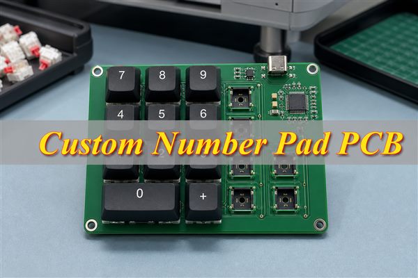
A custom number pad PCB combines the key-switch circuit, controller, interface and optional lighting or wireless functions in a board shaped for a specific keypad. Releasing it for production requires four matching elements: switch footprints aligned with the plate and enclosure, firmware mapped to the matrix, a verified USB or wireless interface, and repeatable functional-test criteria.
EBest Circuit supports custom number pad PCB prototyping, fabrication and assembly for projects that need USB-C, hot-swap sockets, programmable keys or wireless functions. Send your layout, Gerber files, BOM, firmware requirements, mechanical drawings and order quantity to sales@bestpcbs.com for a manufacturability review and quotation.
What Is a Custom Number Pad PCB and How Does It Work?
A custom number pad PCB detects key presses through a switch matrix, converts them into commands and sends those commands to a computer or host system. The board can be a simple wired numeric keypad, a programmable macro pad, a wireless data-entry device or part of an industrial control panel.
Most designs arrange switches into rows and columns. When a key closes, the controller identifies the connected row and column. A diode at each switch controls current direction and reduces ghosting when several keys are pressed. Firmware then maps that switch position to a number, command, shortcut or macro.
The PCB locates switches, stabilizers, LEDs, encoders, displays, connectors and mounting holes. Electrical and mechanical design must therefore be checked together: a working circuit can still fail assembly if the USB connector misses the enclosure opening or a socket collides with a mounting boss.
During a key scan, the controller drives one matrix line at a time and reads the others. Firmware filters contact bounce, applies the selected key map and sends the resulting USB or wireless report. This signal path creates four separate verification points: switch continuity, diode direction, matrix coordinates and host output. Checking all four makes it possible to distinguish a soldering fault from a routing or firmware error.
Which Custom Number Pad PCB Type Fits Your Application?
Custom number pad PCBs are best classified by system architecture: wired fixed-function, wired programmable, wireless programmable or host-integrated industrial. Hot-swap sockets are a switch-mounting option that can be added to wired or wireless programmable designs, not a separate PCB class.
| System Architecture | Host Connection | Control and Switch Options | Best Fit | Main Trade-Off |
| Wired fixed-function | USB-C or fixed cable | Preset key map; soldered switches are typical | Stable numeric entry with no user remapping | Simple to control, but later function changes require firmware or hardware revision |
| Wired programmable | USB-C | QMK, VIA or custom firmware; soldered or hot-swap switches | Macros, layers, shortcuts and configurable input | Requires controller compatibility, programming access and firmware control |
| Wireless programmable | Bluetooth or other selected radio | Programmable control; soldered or hot-swap switches | Portable or cable-free products | Adds antenna, battery, charging, sleep-current and regulatory requirements |
| Host-integrated industrial | USB, serial or host-specific interface | Fixed or programmable functions matched to the host system | Equipment panels, terminals and access-control interfaces | Connector retention, ESD strategy and acceptance tests are application-specific |
Choose the architecture first, then specify soldered or hot-swap switches, lighting, encoders and displays as options within that architecture. This prevents overlapping features from being treated as incompatible PCB types.
What Should Be Defined Before Starting a Custom Numpad PCB Design?
Define the product requirements before drawing the schematic because key count, layout, connection, firmware and enclosure decisions control the entire board. A written input sheet prevents late changes that alter footprints, controller pins, board outline or assembly cost.
- Lock the key layout. Record the number of keys, key-unit spacing, rotated switches, stepped keys, 2U keys and any nonstandard left-hand arrangement.
- Select the switch system. Define soldered or hot-swap switches, switch family, plate-mounted or PCB-mounted construction and required stabilizers.
- Define user functions. List numeric input, shortcuts, layers, custom macros, rotary encoders, displays, RGB lighting and status indicators.
- Choose the connection. State whether the product uses USB-C, a fixed cable, Bluetooth or another host interface.
- Set the power architecture. Identify USB power, battery type, charging method, sleep behavior and the maximum expected LED load.
- Freeze the mechanical envelope. Provide the board outline, mounting points, connector opening, plate file, enclosure model and maximum component heights.
- Define firmware ownership. Confirm who supplies the source code, compiled firmware, key map, bootloader and programming instructions.
- Define production acceptance. Specify which electrical, programming, key, LED, wireless and current tests determine whether an assembled board passes.
How Should a Custom Number Pad PCB Switch Matrix Be Designed?
Design the switch matrix from the physical key map, required simultaneous-key behavior, available GPIO pins and firmware scan direction. A 4 × 5 matrix supports 20 positions with nine row-and-column signals, reducing pin use compared with direct wiring while keeping each key individually identifiable.
- Create a physical key map. Give every switch a reference designator and record its row, column, key size and firmware position. Include encoders, layer keys and any alternate-layout positions so no input is assigned only in firmware.
- Choose practical matrix dimensions. Select row and column counts that fit the controller’s available GPIO pins and produce clear routing. Compare candidate arrangements before fixing the schematic; a balanced matrix is not useful if it creates long crossings around the connector, LEDs or mounting holes.
- Confirm the scan direction. Decide whether firmware drives columns and reads rows or drives rows and reads columns. Use the same direction in the schematic net names, diode orientation and firmware configuration.
- Use one diode per key for multi-key operation. Per-key diodes prevent unintended current paths when several switches close at once. Match the diode footprint polarity mark, assembly drawing and firmware setting so correctly soldered parts cannot be installed in the wrong direction.
- Separate matrix and lighting circuits. Keep row and column routes away from LED power switching, high-current RGB paths and noisy regulators where practical. Provide stable return paths and follow the controller reference design for pull resistors, reset and interface protection.
- Provide diagnostic access. Add accessible row, column, power, reset and programming points when fixture testing or fault isolation is required. Test access allows an open switch, reversed diode or broken matrix trace to be located without probing under installed switches.
- Control debounce and scan behavior in firmware. Verify that the scan rate, debounce method, layer handling and simultaneous-key behavior match the intended use. Test normal typing, held keys, rapid repeated input and required key combinations on the assembled prototype.
- Cross-check all released files. Compare switch references, net names, matrix coordinates, diode direction and controller pins across the schematic, PCB and firmware definition. Generate a matrix verification sheet that states the expected host output for every physical key.
Typical failures include swapped key positions, a complete dead row or column, ghost inputs and keys that work only in one firmware build. Diagnose them in order: check switch continuity, diode polarity, row and column continuity, controller pin assignment and final key-map output. This sequence separates assembly defects from PCB routing and firmware errors.
How Should USB-C and Wireless Connectivity Be Designed for a Custom Numpad PCB?
USB-C and wireless designs require different power, protection, placement and test plans. USB-C prioritizes connector anchoring, correct USB-C pin configuration, ESD protection and data routing. Wireless designs add antenna clearance, battery safety, charging control and low-power firmware.
USB-C Numpad PCB Design
- Define the USB-C device role. A typical wired numpad is a USB 2.0 peripheral that receives 5 V from the host, so configure it as an upstream-facing port and power sink. Unless a USB-C or power-delivery controller requires another implementation, connect separate 5.1 kΩ Rd pull-down resistors from CC1 and CC2 to ground so the numpad is detected in either plug orientation. Do not use Rp pull-ups, which advertise a power-source role.
- Join the duplicated USB 2.0 contacts correctly. On a full USB-C receptacle, connect A6 and B6 to the same D+ net and A7 and B7 to the same D− net close to the connector, then route D+ and D− as one differential pair to the controller. Verify the exact receptacle pinout because connector symbols and reduced-pin USB 2.0 receptacles can differ.
- Control the connector mechanically. Position the receptacle from the final enclosure datum. Verify shell tabs, locating posts, insertion direction, cable clearance, board-edge distance and support against repeated cable force.
- Protect power and data lines. Place suitable ESD protection close to the receptacle, provide a defined shield connection and size the VBUS path for the intended current. Keep protection-device stubs and the D+/D− route short.
- Route the data pair consistently. Keep D+ and D− together over a continuous reference path, minimize branch length where the duplicated contacts join, avoid unnecessary vias and do not cross plane gaps. Review the controller reference design, receptacle breakout and ESD-device layout before fixing the route.
- Verify the assembled interface. Test enumeration, every key function, cable movement and connector alignment with the final firmware and representative enclosure. A continuity check alone cannot confirm stable host communication.
Wireless Numpad PCB Design
- Select the radio architecture. Confirm the controller or module, supported firmware, antenna type, programming method and target-market requirements before layout. Module approval does not remove the need to review the final antenna implementation and product configuration.
- Protect the antenna area. Follow the radio supplier’s keepout dimensions and placement guidance. Keep copper, batteries, displays, cables, metal fasteners and enclosure features out of restricted antenna regions.
- Design the complete power path. Match battery chemistry, protection, charging circuit, connector and charge current. Calculate active, LED-on, sleep and charging current separately so firmware power states and expected operating time can be evaluated.
- Plan battery and enclosure integration. Verify battery space, cable routing, service access, heat sources and mechanical retention in the 3D assembly. The enclosure material and nearby metal parts can change radio performance.
- Test the finished wireless product. Check pairing, reconnection, input response, operating range, sleep current and charging behavior with the intended battery and enclosure. Open-board range is not representative of the final assembly.
How Can a Programmable Custom Number Pad PCB Support QMK, VIA and Custom Macros?
A programmable custom number pad PCB needs a supported controller, correct matrix definition, sufficient firmware resources and a controlled programming process. QMK can implement layers, tap functions, rotary encoders and custom key behavior. VIA can allow compatible key maps to be changed without rebuilding firmware, while application-specific macros can be implemented in firmware or host software.
- Controller support: verify that the selected microcontroller, bootloader and available pins match the intended firmware before finalizing the PCB.
- Matrix definition: keep row pins, column pins, diode direction and physical layout consistent across the schematic, PCB and firmware files.
- Programming access: provide an accessible reset or boot method and the pads or connector required by the chosen programming process.
- Version control: identify the firmware filename, version, checksum and approved key map on the production package.
- Functional limits: confirm memory use, LED current, encoder behavior, sleep mode and wireless functions on the actual assembled prototype.
The production package should contain the approved compiled file, version, checksum, programming voltage, access location and readback method. Assign each key-map variant a distinct part number or configuration code. Test macros that depend on host software, operating-system permissions or timing in the target environment; continuity testing cannot detect an incorrect pin map or bootloader.
How Should Hot-Swap Socket, Switch and Stabilizer Clearances Be Set?
Clearances must be checked as a complete mechanical stack that includes the PCB, socket, switch, plate, stabilizer, enclosure and nearby components. A correct schematic symbol does not prove that a hot-swap socket can be soldered, that a switch will seat fully or that a stabilizer will move without interference.
- Use the approved socket footprint. Confirm pad shape, socket orientation, switch-pin holes and manufacturer drawing against the selected part number.
- Check the underside keepout. Prevent sockets from colliding with mounting posts, batteries, controller modules, connectors or enclosure ribs.
- Confirm stabilizer format. Match PCB-mounted or plate-mounted stabilizers to the plate cutout, switch position and large-key orientation.
- Verify plate-to-PCB spacing. Model the switch, plate, PCB and any foam or gasket that changes seating depth.
- Protect solder joints. Avoid flexing the PCB during switch insertion and removal, and review pad support around sockets near the board edge.
- Inspect with a 3D assembly. Overlay the PCB model, plate drawing and enclosure before prototype release, then physically test representative keys on the first assembly.
Use dimensions from the selected socket, switch and stabilizer drawings instead of a visually similar library footprint. The mechanical review should include solder-joint access, tool access for rework and the direction of force during switch replacement. On the first assembled unit, inspect representative center and edge sockets before installing all switches; edge locations often experience the greatest board flex.
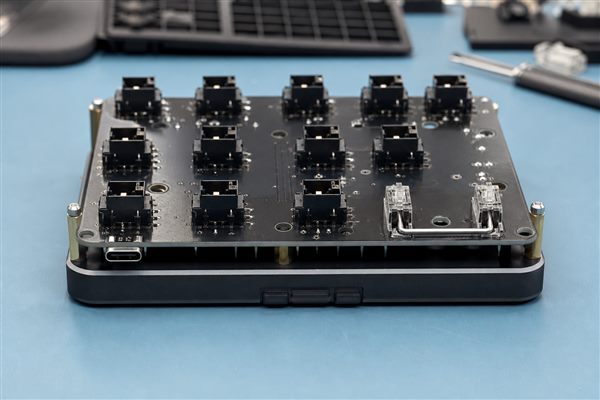
Which PCB Materials, Layer Counts and Surface Finishes Suit a Mechanical Numpad PCB?
FR-4 is the normal starting material, while layer count and surface finish should follow routing, wireless, connector and assembly needs. A simple wired matrix can often be routed on two layers. Four layers can provide cleaner power and ground distribution when the board adds dense lighting, a wireless module, a display or more demanding routing.
| Construction Choice | When It Fits | Main Benefit | Main Trade-Off | What to Confirm |
| Two-layer FR-4 | Basic wired matrix and moderate component count | Simple, economical construction | Less routing and plane flexibility | Ground return paths and connector routing |
| Four-layer FR-4 | Wireless, dense RGB, display or compact routing | Dedicated plane options and easier routing control | Higher fabrication cost than two layers | Final stackup and antenna requirements |
| HASL finish | General through-hole or larger-pitch assembly | Common and practical | Surface planarity is less uniform than ENIG | Fine-pitch pads and socket assembly needs |
| ENIG finish | Fine-pitch parts, flat pads and mixed assembly | Flat solderable surface | Higher cost than common HASL options | Project storage and assembly requirements |
| OSP finish | Flat copper pads with a defined assembly flow | Flat surface with a thin coating | Handling and storage controls matter | Assembly timing and rework plan |
EBest Circuit’s general PCB capability workbook lists standard FR-4 production from 1 to 10 layers, with 8-layer and higher standard builds requiring high-Tg material. It lists 10 to 32 layers as a special process range. For a number pad, extra layers should solve a real routing, plane or wireless requirement rather than serve as a generic quality upgrade.
Board thickness is also a mechanical input because it affects switch seating, USB connector alignment, stiffness and the available space below the plate. Copper weight should follow current and routing needs rather than be increased by default. Select the surface finish with the smallest assembled pads and planned storage interval in mind, then confirm solder-paste design and reflow compatibility for fine-pitch USB parts, LEDs and hot-swap sockets.
What Should Be Verified on a Custom Number Pad PCB Prototype?
A custom number pad PCB prototype must verify electrical operation, mechanical fit, firmware behavior and the proposed production test, not merely power on. Approval should use a written checklist so that a repaired sample does not become the undocumented reference for later production. This validation sequence complements the broader controls used for a fast-turn PCB prototype.
- Inspect the bare board. Confirm outline, slots, mounting holes, connector position, surface finish, solder mask openings and identification marks.
- Check assembly orientation. Verify diodes, controller, USB components, LEDs, sockets, encoders and polarized parts against the assembly drawing.
- Power the board safely. Check for shorts and abnormal current before connecting the complete product.
- Program the approved firmware. Record the build version and verify that the boot or reset method remains accessible.
- Test every input. Exercise all keys, layers, macros, encoders and special functions, including combinations that could reveal ghosting or mapping errors.
- Verify the interface. Test USB enumeration and cable movement, or wireless pairing, reconnect behavior and current consumption as applicable.
- Assemble the mechanics. Fit the PCB with the final plate, switches, stabilizers, keycaps, enclosure and battery to identify interference.
- Close all deviations. Update Gerber, BOM, drawings, firmware and revision records before approving low-volume production.
Record the result for every checklist item instead of using a single “prototype passed” decision. The approval record should identify the PCB revision, BOM revision, firmware checksum, enclosure revision and any rework performed. A repaired unit may prove the proposed correction, but repeat production should use updated source files and a clean build rather than rely on undocumented jumper wires or component changes.
How Are Custom Number Pad PCBs Manufactured and Assembled?
Production converts the released data package into bare boards, assembled PCBAs, programmed units and test records through a controlled sequence. The exact route depends on whether the design combines SMT electronics, through-hole switches, hot-swap sockets, controller modules, displays or manual hardware.
- Review the data package. Check Gerber or ODB++, drill files, stackup, BOM, centroid data, assembly drawings, firmware and acceptance criteria.
- Complete DFM and DFA review. Identify footprint, polarity, clearance, panelization, solder-mask, test-access and mixed-assembly risks before release.
- Prepare the production panel. Select panel rails, tooling holes, fiducials and routing or V-cut methods that support assembly and depanelization.
- Fabricate the bare PCB. Process imaging, etching, drilling, plating, solder mask, legend, surface finish, profiling and electrical testing under the approved construction.
- Source and verify components. Match manufacturer part numbers, packages and approved alternatives, with special attention to controllers, USB connectors, radio modules and hot-swap sockets.
- Assemble SMT components. Print solder paste, place components, reflow and inspect the board before operations that reduce access.
- Complete through-hole and manual assembly. Install switches, headers, encoders, modules or connectors according to the approved route.
- Program, clean and test. Load the approved firmware, inspect workmanship and run the specified electrical and functional tests before packing.
Sequence the operations around access and heat exposure. Fine-pitch USB parts, controllers and LEDs are normally inspected before large switches, sockets or modules restrict the view. Manual operations need defined orientation and solder criteria, while programming must use the released firmware identity. Final cleaning requirements depend on the flux and assembly route, and completed boards should be protected against connector or switch damage during packing.
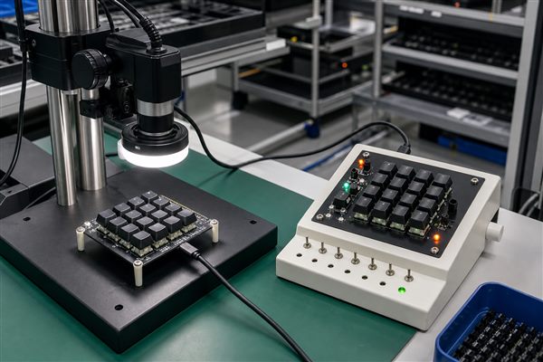
What Changes When a Custom Number Pad PCBA Moves to Low-Volume Production?
Low-volume production replaces prototype flexibility with documented materials, fixtures, test limits and revision control. The objective is to reproduce the approved behavior without relying on manual knowledge from the first build.
| Control Point | Prototype Build | Low-Volume PCBA | Reason for the Change |
| BOM | Parts may be purchased in small quantities | Manufacturer part numbers and approved alternates are frozen | Prevents uncontrolled substitutions |
| Panelization | Single boards may be acceptable | Panel format supports placement, handling and depanelization | Improves repeatability and throughput |
| Programming | Manual loading may be used | Firmware file, version and work instruction are controlled | Prevents mixed firmware |
| Testing | Bench checks may find obvious faults | Fixtures or repeatable procedures apply defined pass limits | Creates consistent acceptance |
| Change control | Rework may be exploratory | All changes update design files, BOM, firmware and revision marks | Keeps repeat orders traceable |
Approve a golden sample or equivalent reference, close every prototype deviation and verify the panel, assembly sequence, programming and test method in a short pilot batch. Track failures by cause. Any component alternate must be checked for footprint, pinout, firmware, electrical behavior and height, then recorded across the affected fabrication, BOM, placement, drawing, firmware and test files.
Which Tests Should a Custom Number Pad PCBA Pass?
A reliable test plan must prove board integrity, correct programming and the behavior of every user input and interface. Test coverage should reflect the actual product configuration rather than apply the same generic checklist to wired, wireless and RGB designs.
| Test Stage | What Is Checked | Typical Failure Found | Acceptance Evidence |
| Bare-board electrical test | Continuity and isolation of PCB nets | Open or short circuit | Electrical test result for the fabricated board |
| Visual or automated inspection | Polarity, placement and solder-joint condition | Missing, shifted, reversed or poorly soldered part | Inspection result under the agreed assembly criteria |
| Programming verification | Firmware identity and successful loading | Wrong build, failed programming or inaccessible boot mode | Recorded firmware version or checksum |
| Matrix and full-key test | Every switch position and key combination | Open key, swapped position, wrong diode or ghosting | Pass record for all defined inputs |
| Interface test | USB enumeration or wireless pairing and reconnect | Unstable connection or interface configuration error | Functional connection result |
| Feature test | LEDs, encoders, display, macros and layers | Wrong mapping, color, direction or function | Approved function checklist |
For wireless designs, add operating, sleep and charging-current checks with the intended battery system. For USB-C designs, test enumeration and physical connector behavior with the representative enclosure. Environmental or lifecycle testing should be defined only when the final application’s risk and service conditions require it.
Each test needs a defined setup, expected result and disposition rule. “Key works” is insufficient when the required output, layer or macro is unclear. Map every physical position to its expected report and log failed coordinates. For hidden socket or connector joints, decide during DFM whether electrical coverage, X-ray inspection or a mechanical check is required.
What Determines Custom Number Pad PCB Cost and Lead Time?
Cost and lead time depend on board construction, component availability, assembly mix, firmware handling, test coverage and order quantity. A small PCB is not automatically a simple PCBA if it contains a scarce controller, fine-pitch USB components, hot-swap sockets, a display and manual through-hole work.
- PCB construction: layer count, board thickness, copper weight, surface finish, outline complexity and panel utilization affect fabrication.
- Component sourcing: controller, radio module, connector, hot-swap socket and display availability can control the schedule.
- Assembly route: SMT, through-hole soldering, hand-installed modules and mechanical hardware require different operations.
- Programming: custom firmware, bootloader handling, serialization or multiple variants add preparation and control work.
- Testing: full-key fixtures, wireless checks, LED inspection and current measurements add coverage but reduce escaped defects.
- Quantity and variants: several layouts, colors or firmware versions can split material and setup across smaller batches.
- File readiness: unresolved footprints, missing centroid data or unclear substitutions delay review and quotation.
Compare quotations by separating bare PCB, components, assembly, programming, testing and one-time tooling. Cost can often be reduced by consolidating variants, using available packages, improving panel utilization and standardizing firmware and testing. Lead time is most exposed to controllers, radio modules, displays and special connectors, so approve suitable alternatives before sourcing begins.
What Files Are Needed for a Custom Number Pad PCB Quote?
A complete quote package should describe the bare PCB, every assembled part, mechanical interfaces, firmware and test expectations. Missing information forces assumptions that can change price, schedule or deliverable scope later.
- PCB fabrication data: Gerber or ODB++ files, NC drill files, board outline, layer count, thickness, copper weight, solder-mask color, legend and surface finish.
- Bill of materials: reference designators, quantity, manufacturer name, manufacturer part number, package and approved alternatives.
- Placement data: centroid or pick-and-place file with side, X/Y position and rotation.
- Assembly drawings: polarity, do-not-fit parts, socket orientation, connector details and manual assembly notes.
- Mechanical files: plate drawing, enclosure model, mounting points, connector opening and height limits when fit is part of the review.
- Firmware package: approved binary, version, programming method, boot instructions and required configuration data.
- Test requirements: full-key map, USB or wireless behavior, LED and encoder functions, current limits and required records.
- Commercial inputs: prototype quantity, low-volume quantity, target schedule, delivery location and required packaging.
All files should carry the same revision and use consistent reference designators. The BOM must distinguish customer-supplied, manufacturer-sourced and do-not-fit parts, while the placement file must match the assembly side and board origin used in the drawings. If the quotation includes programming or functional testing, provide executable files and expected outputs, not source code alone.
How Should You Compare Custom Keypad PCB Manufacturers and Suppliers?
Compare suppliers by the controls included in the quoted scope and the evidence they can return, not by the total price alone. Use the following checks to identify omitted work, uncontrolled substitutions and test gaps before selecting a source.
- Review the DFM and DFA scope. Ask whether the review covers footprints, solder-mask openings, hot-swap socket orientation, stabilizer and enclosure clearances, connector access, panelization and test access. Strong evidence is a marked review tied to your submitted revision; a generic “files are manufacturable” response does not show which risks were checked.
- Confirm component control. Require manufacturer part numbers for the controller, USB connector, radio module, LEDs, sockets and other function-critical parts. Proposed alternatives should need approval after pinout, package, electrical rating, height and firmware impact are checked.
- Define every assembly operation. Identify which party handles SMT, through-hole soldering, hot-swap sockets, switches, encoders, displays, headers and mechanical parts. This prevents a low quotation from excluding manual operations that are essential to the finished unit.
- Verify programming responsibility. State who supplies the binary, bootloader and configuration files; how the approved version is identified; and whether programming success is read back. Request a record containing the firmware version or checksum when traceability is required.
- Specify functional-test coverage. Confirm whether testing covers every key position, layers, macros, encoders, LEDs, USB enumeration or wireless pairing, and current measurements. Agree on the fixture, pass limits and result format instead of accepting “functional test included” without a test definition.
- Check prototype-to-production control. Ask how prototype rework, BOM changes and firmware corrections are transferred into repeat orders. Strong control keeps Gerber, BOM, placement, assembly drawing, firmware and test revisions aligned with the approved sample.
- Separate one-time and recurring costs. Request individual lines for bare PCBs, components, assembly, programming, testing, fixtures, tooling and customer-supplied-part handling. Quotations are comparable only when they cover the same operations and deliverables.
- Review sample evidence. Before ordering, request one representative DFM response and one test-record example with confidential details removed. The format should show that issues, revisions, pass limits and results can be recorded clearly.
Why Choose EBest Circuit as Your Custom Number Pad PCB Manufacturer?
EBest Circuit reviews the PCB data, BOM, mechanical constraints, firmware and test requirements together, helping prevent late footprint changes, unapproved substitutions and missing assembly operations. The quotation can then identify included fabrication, sourcing, programming, manual assembly and testing work before the order is released.
- Reduce avoidable revisions: free DFM review can identify footprint, spacing, panelization, connector and assembly concerns before fabrication.
- Simplify project coordination: PCB fabrication, component sourcing, SMT assembly, through-hole work, programming and functional testing can be evaluated within one project package.
- Protect BOM intent: manufacturer part numbers and proposed alternatives can be reviewed before substitution, reducing pinout, package and firmware risks.
- Improve prototype decisions: the review can connect design files, plate and enclosure constraints, firmware and test expectations instead of checking the bare board alone.
- Prepare for repeat orders: controlled Gerber, BOM, assembly drawing, firmware and test revisions help keep later low-volume batches aligned with the approved design.
- Match capability to the project: standard and special PCB processes are separated during review so nonstandard construction is confirmed rather than assumed.
Submit the fabrication package, BOM, placement data, mechanical constraints, firmware and acceptance checklist together. EBest Circuit can identify missing inputs and special-process requirements before prototype or low-volume release.
FAQs About Custom Number Pad PCBs
Q1: Are per-key RGB lighting and RGB underglow the same feature?
A1: No. Per-key RGB places an LED at each switch, while underglow places LEDs on the PCB underside to illuminate the case or desk surface. They use different footprints, optical paths and power budgets, so the required lighting effect must be stated before layout.
Q2: Can one numpad PCB support both 1U and 2U key positions?
A2: It can when alternate switch holes, hot-swap sockets and stabilizer locations do not conflict. Each supported arrangement needs a defined plate and assembly variant; otherwise an electrically valid option may be impossible to assemble.
Q3: Does a hot-swap PCB automatically support every alternate layout?
A3: No. A hot-swap socket fixes the switch position and orientation, so overlapping layouts may require separate PCB variants or soldered positions. Layout support must be confirmed from the exact footprint and plate combination, not from the term “hot-swap.”
Q4: Does a USB-C daughterboard make a numpad PCB compatible with any enclosure?
A4: No. A daughterboard separates the USB opening from the main PCB, but it does not make the main PCB universally enclosure-compatible. Compatibility still depends on the board outline, mounting pattern, internal height, cable path, daughterboard location and case fastening method.
Q5: Can soldered and hot-swap versions use the same firmware file?
A5: Sometimes, if both versions use the same controller pins, matrix coordinates, diode direction and optional-feature assignments. Firmware compatibility must be verified against both schematics; similar key layouts do not prove identical electrical mapping.
Q6: What keeps a hot-swap PCB and plate together when all switches are removed?
A6: The enclosure may use PCB screws, plate fasteners, standoffs or retention features independent of the switches. If switches provide most of the retention, removing them together can let the PCB separate or flex, so the mechanical design should support the PCB independently of the switches.
Q7: Can low-profile switches use a standard MX hot-swap footprint?
A7: Usually not. Low-profile and MX switch systems generally require different verified footprints because their pin positions, stabilizers, plate openings and sockets can differ. Select the exact switch and socket part numbers before creating the PCB and plate libraries.
Q8: Can a custom numpad support both wired and wireless operation?
A8: Yes, when the controller, power-path selection, battery charging, USB interface and firmware support both modes. The power path must prevent uncontrolled interaction between USB and battery power, and the design must define mode switching and operation while USB is connected.
Q9: Can a USB hub be added to a custom number pad PCB?
A9: Yes, but it requires a suitable hub controller, additional USB routing, ESD protection, connector space and a complete power budget. Every downstream port must be tested for enumeration and current behavior while the numpad operates at maximum lighting load.
Q10: Can the same numpad PCB be used for right-hand and southpaw layouts?
A10: It is possible with a reversible main PCB, separate left/right variants or a daughterboard architecture that preserves connector access. Both orientations need independent mechanical and electrical verification, including diode direction, component-side clearance, stabilizer positions, firmware mapping and enclosure mounting.
Ready to request a custom number pad PCB quotation? Send your Gerber or ODB++ data, BOM, placement file, assembly drawings, firmware requirements, test checklist, prototype quantity and low-volume forecast to EBest Circuit at sales@bestpcbs.com.