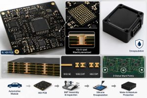
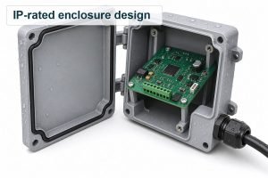
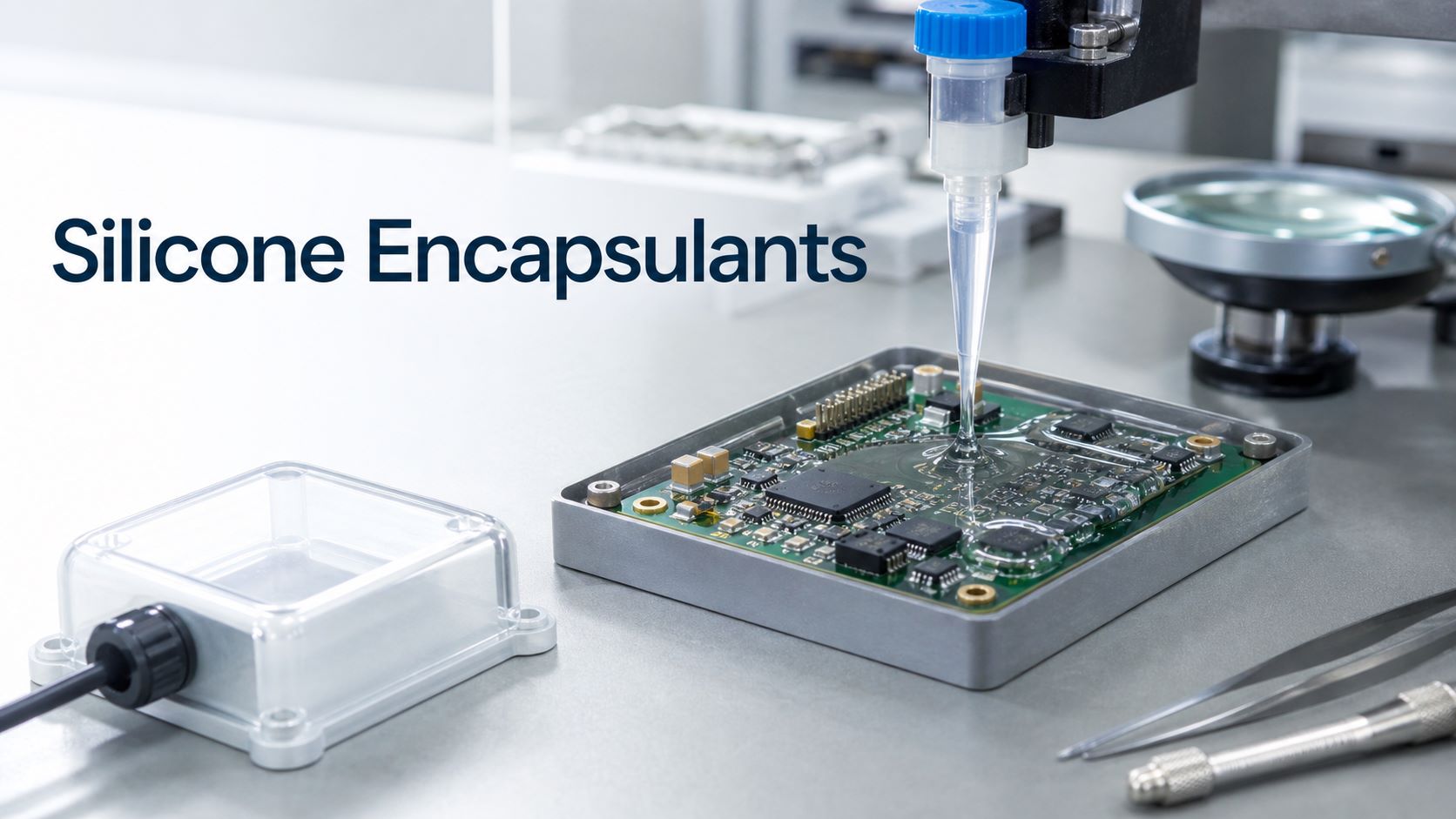
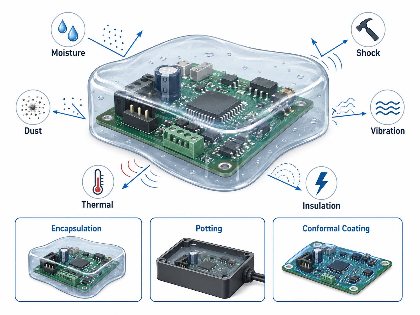
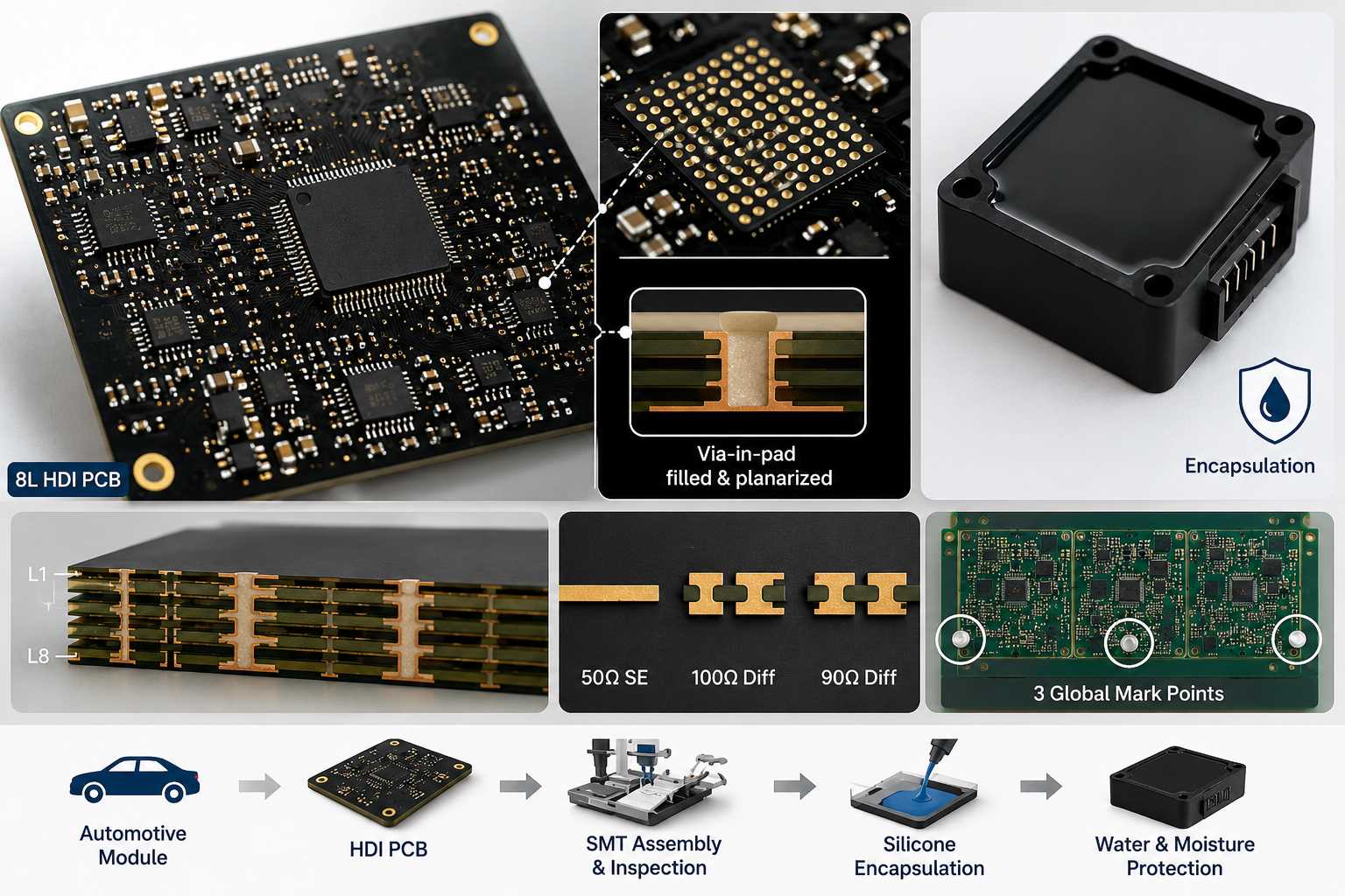
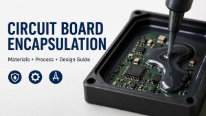
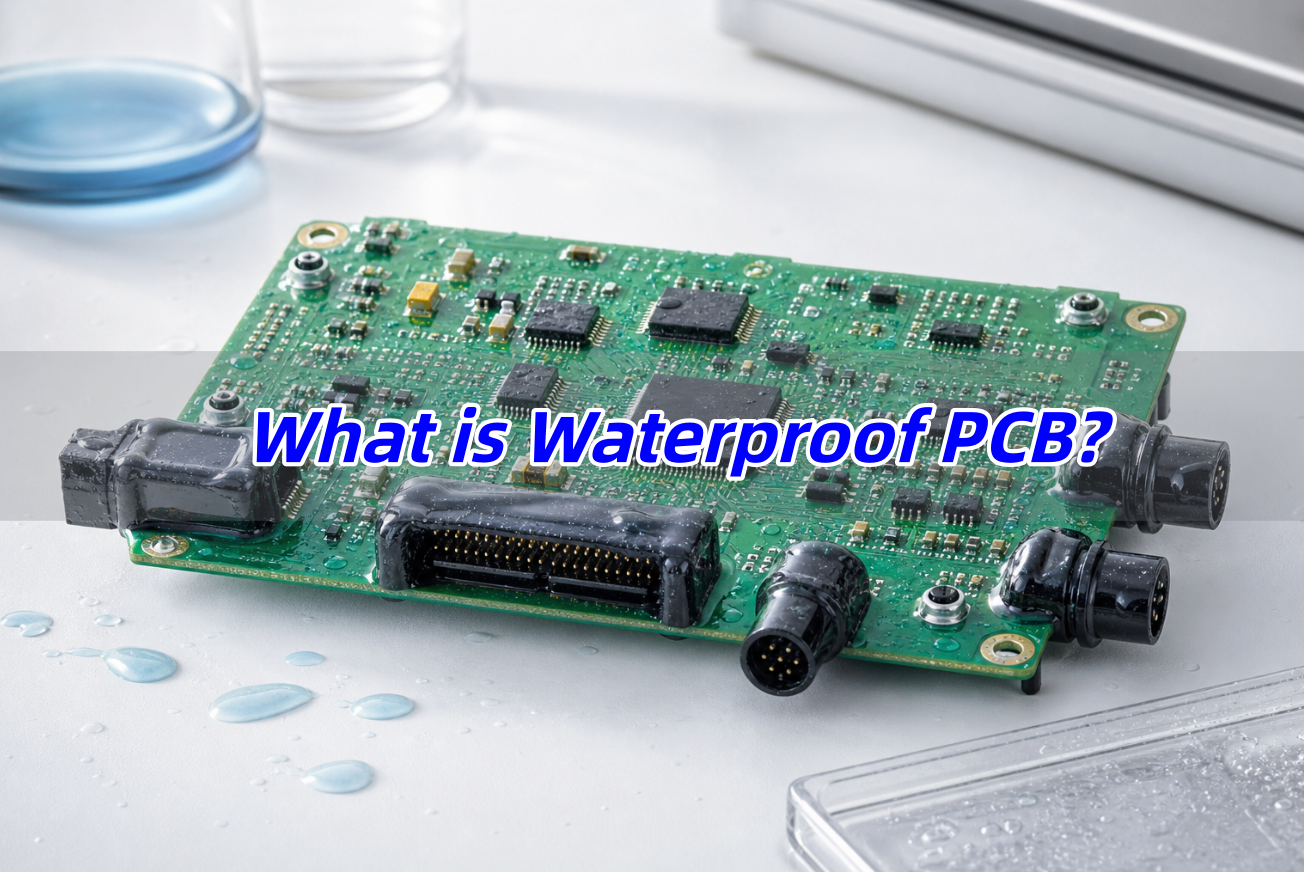
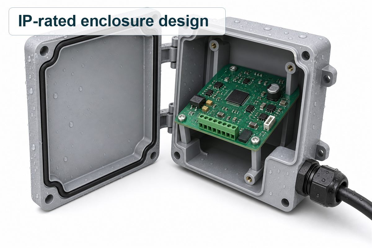
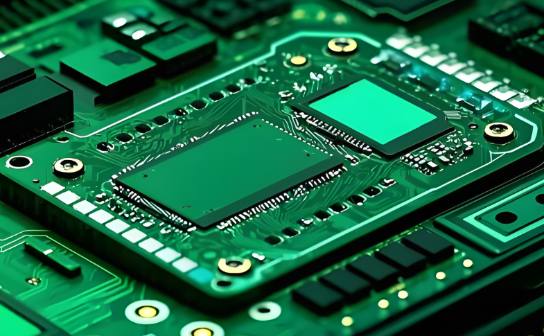
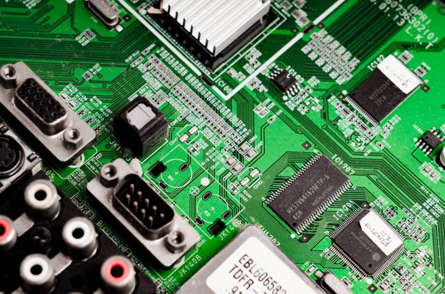
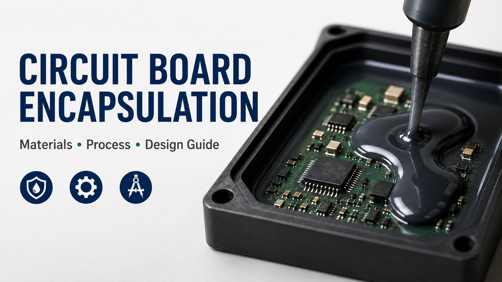
circuit board encapsulation protects a PCB or PCBA with epoxy, silicone, polyurethane, gel, or another protective compound. It helps resist moisture, chemicals, vibration, corrosion, and electrical leakage in automotive, industrial, outdoor, marine, and high-voltage electronics.
Reliable encapsulation depends on more than resin selection. Material viscosity, hardness, curing, heat transfer, masking, air release, test access, and repair requirements must be reviewed together. This guide covers the materials, methods, potting process, DFM rules, defects, and testing requirements. Have an encapsulation project? Send your Gerber files, BOM, enclosure drawing, and operating requirements to sales@bestpcbs.com for an engineering review and quotation.
What Is Circuit Board Encapsulation?
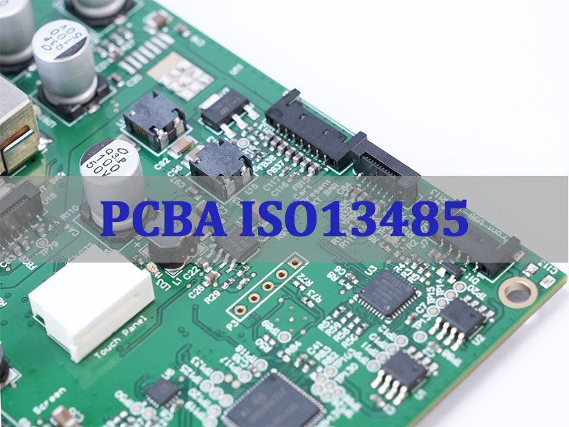
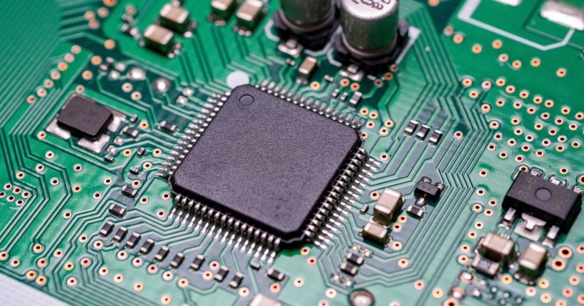
Circuit board encapsulation is the process of covering a printed circuit board, assembled PCBA, or selected component area with a protective material that cures into a solid, flexible, or gel-like layer.
An encapsulated circuit board may use:
- Full enclosure filling
- Partial or selective encapsulation
- Dam-and-fill around a component group
- Glob top protection over an IC
- Gel filling for sensitive electronics
- Low-pressure molding around the assembly
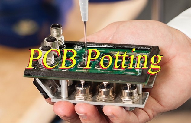
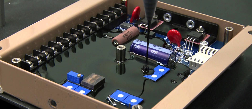
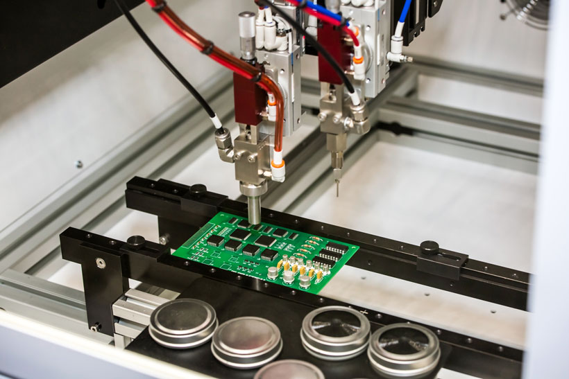
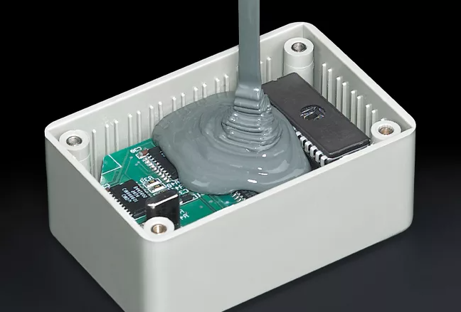
Encapsulation is the broad protective concept. Potting is a common method in which liquid compound is dispensed into a housing, mold, or cavity that contains the material while it cures.
The purpose is not always to make the PCB completely waterproof. The selected protection method must match the operating environment, electrical requirements, thermal load, expected service life, enclosure structure, and repair policy.
When Does a PCB or PCBA Need Encapsulation?
Encapsulation is normally considered when an enclosure or conformal coating cannot provide enough environmental, electrical, or mechanical protection.
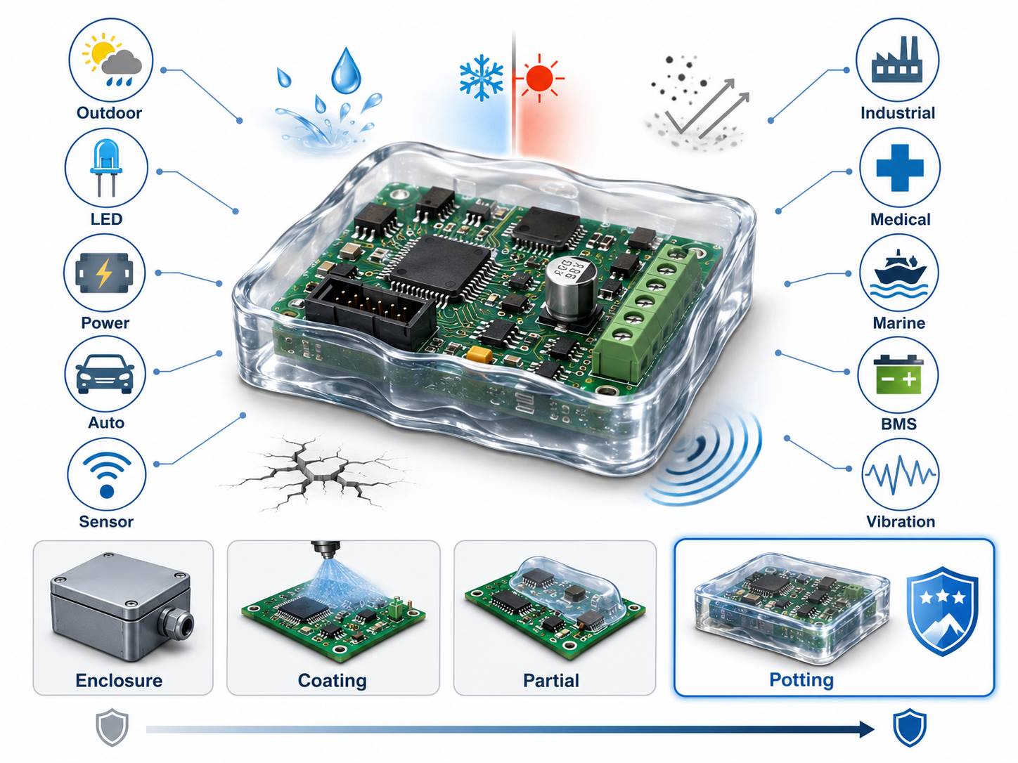
Typical applications include:
- Outdoor control modules
- Automotive electronic assemblies
- LED drivers and lighting controls
- Industrial power supplies
- Battery management systems
- Marine electronics
- High-voltage modules
- Railway and transportation equipment
- Sensors exposed to humidity or contamination
A PCBA may need encapsulation when it faces condensation, salt spray, chemicals, vibration, mechanical impact, wide temperature changes, or additional dielectric-isolation requirements.
Full potting is not automatically the best solution. It increases weight, material consumption, curing time, and repair difficulty. It can also change how heat moves from components to the enclosure.
A practical selection process is:
- Identify the dominant environmental risk.
- Determine whether the risk affects the full assembly or only one area.
- Review voltage, heat, vibration, and mechanical requirements.
- Decide whether the product must remain repairable.
- Select the least complex protection method that meets the reliability target.
For light condensation, conformal coating may be sufficient. Selective encapsulation may protect only a high-voltage or moisture-sensitive section. Full potting is more appropriate when the entire assembly needs environmental sealing and mechanical support.
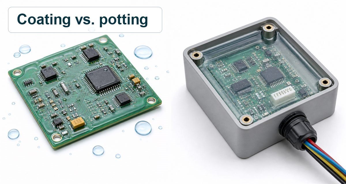
Potting vs Encapsulation vs Conformal Coating: What Changes in Production?
These terms are related, but they describe different protection structures and production controls.
| Protection method | Structure | Main advantage | Main limitation |
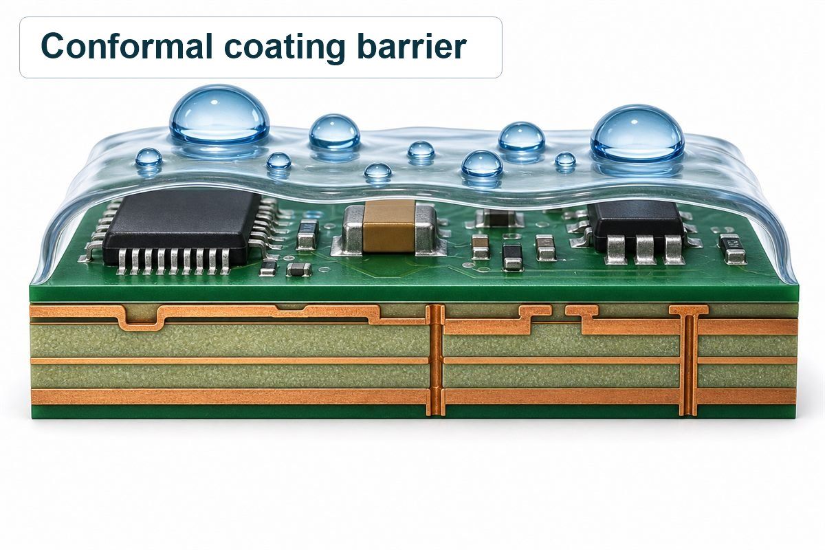
| Conformal coating | Thin film covering the PCB surface | Low weight and easier inspection | Limited mechanical support |
| Full potting | Compound fills an enclosure or cavity | Strong environmental and vibration protection | Difficult rework and higher material use |
| Selective encapsulation | Resin covers one defined area | Protects only the high-risk zone | Requires accurate masking and dispensing |
| Low-pressure molding | Molded material surrounds the assembly | Repeatable sealing and geometry | Requires tooling and process validation |
Conformal coating follows the contours of the PCB and components. Potting creates a much thicker protective mass around components, solder joints, and wires.
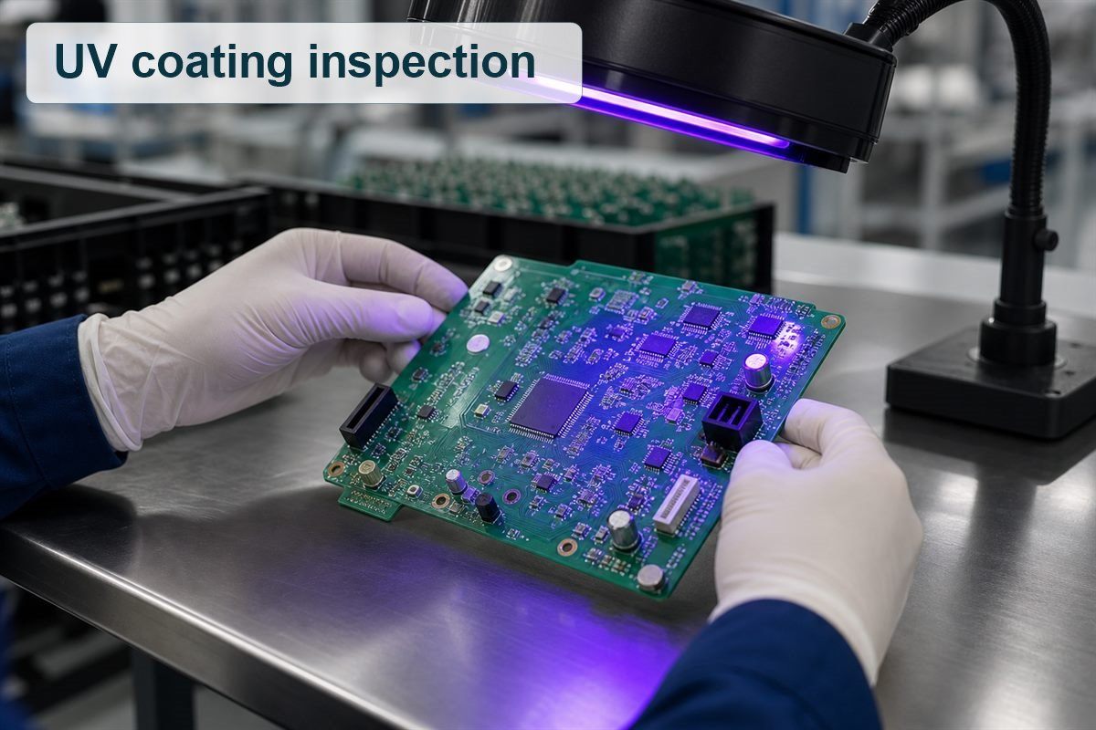
The manufacturing controls also differ. Conformal coating focuses on coverage, thickness, masking, curing, and coating inspection. PCB potting additionally requires:
- Resin-to-hardener ratio control
- Material temperature management
- Vacuum degassing when required
- Resin-flow planning
- Fill-height control
- Cure-exotherm management
- Pre-potting functional testing
- Post-cure electrical verification
The expected failure mode should determine the choice. Condensation may only require conformal coating. Heavy vibration, chemical exposure, or high-voltage isolation may justify full circuit board encapsulation.
Which Materials Are Used for Circuit Board Encapsulation?
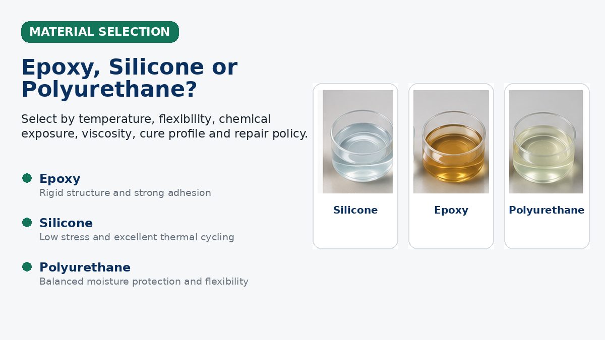
The main circuit board potting materials are epoxy, silicone, and polyurethane. Silicone gel and specialty thermally conductive compounds are also used for specific electrical, mechanical, or thermal requirements.
Epoxy encapsulants
Epoxy normally cures into a hard, rigid structure. It offers strong adhesion, chemical resistance, dielectric performance, and mechanical support.
Typical applications include:
- Industrial control modules
- Transformers and coils
- Relays
- Power electronics
- Permanently sealed assemblies
Its main limitation is rigidity. Cure shrinkage and thermal-expansion mismatch may transfer stress to solder joints, ceramic capacitors, connectors, or component bodies.
Silicone encapsulants
Silicone remains flexible across a broad temperature range. It is often selected for assemblies exposed to thermal cycling, vibration, or temperature extremes.
Common applications include:
- Sensors
- Outdoor electronics
- Automotive modules
- High-temperature assemblies
- Delicate components and solder joints
Silicone generally places less mechanical stress on the assembly than rigid epoxy. However, its flow behavior and adhesion characteristics must be checked against the PCB, enclosure, and masking materials.
Polyurethane encapsulants
Polyurethane provides useful moisture resistance and greater flexibility than rigid epoxy. It is frequently used in outdoor controls and assemblies that need environmental protection without excessive stiffness.
Its properties vary by formulation. Engineers should verify hydrolysis resistance, operating temperature, hardness, chemical resistance, and cure behavior instead of selecting it by material name alone.
Specialty encapsulation materials
Other options include:
- Silicone gel for low-stress protection
- Thermally conductive potting compound
- Flame-retardant encapsulant
- Optically clear resin
- Low-viscosity material for narrow gaps
- Flexible encapsulant for vibration-sensitive assemblies
Epoxy vs Silicone vs Polyurethane: How Should Engineers Choose?
The best PCB encapsulant is the material that fits the assembly, operating environment, and production process.
| Factor | Epoxy | Silicone | Polyurethane |
| Mechanical behavior | Hard and rigid | Soft to flexible | Flexible to semi-rigid |
| Thermal cycling | Moderate | Excellent | Good |
| Moisture resistance | Good | Excellent | Very good |
| Component stress | Higher | Low | Moderate to low |
| Chemical resistance | Strong | Good | Good |
| Reworkability | Difficult | Better with some grades | Limited |
| Typical use | Industrial and power modules | Sensors and high-temperature electronics | Outdoor and mixed-environment controls |
Engineers should compare the following properties:
- Mixed viscosity
- Pot life
- Cure time and temperature
- Cure exotherm
- Hardness
- Coefficient of thermal expansion
- Dielectric strength
- Volume resistivity
- Thermal conductivity
- Water absorption
- Chemical resistance
- Flame-retardant rating
- Reworkability
Viscosity directly affects production yield. A low-viscosity circuit board potting compound can flow beneath dense components but may leak into connectors, screw holes, switches, or cable entries. A high-viscosity material is easier to contain but may leave voids beneath transformers, relays, shields, or tall capacitors.
Large resin volumes also require cure control. Excessive exotherm can deform plastic housings, damage temperature-sensitive parts, or create internal stress. Thick sections may require staged filling or a lower-exotherm formulation.
Thermal conductivity should be reviewed as part of the complete heat path. A thermally conductive resin only helps when it connects the heat-generating component to a suitable enclosure, heat spreader, or heat sink.
Which Circuit Board Encapsulation Method Fits the Assembly?
The encapsulation method should match the board layout, enclosure structure, production quantity, and required protection level.
Full potting
The compound fills most or all of the enclosure. This method provides strong environmental and mechanical protection but increases weight, material cost, and rework difficulty.
It is commonly used for:
- Power modules
- Outdoor controllers
- Transformers
- High-voltage assemblies
- Non-serviceable industrial electronics
Partial encapsulation
Only selected areas are covered. Connectors, calibration points, heat sinks, switches, or repairable components remain accessible.
Partial encapsulation is useful when one section requires protection but the full board does not need to be permanently sealed.
Dam-and-fill
A higher-viscosity material forms a boundary, while a lower-viscosity compound fills the enclosed area. This method helps control resin flow around component groups or sensitive circuits.
The dam must remain stable during dispensing and curing. Its height, adhesion, spacing, and compatibility with the fill material should be validated during prototype production.
Glob top
A controlled amount of encapsulant is placed over a single component, chip, or die. It provides local environmental and mechanical protection without covering the entire PCBA.
Gel encapsulation
A soft gel protects delicate components while placing minimal mechanical stress on wire bonds, solder joints, or sensitive packages.
Low-pressure molding
Thermoplastic material is molded around the assembly at relatively low pressure. It can provide consistent geometry and sealing for higher-volume products but requires tooling and process validation.
For prototypes and small batches, conventional dispensing is often more practical because fill points, material volume, masking, and cure conditions can be adjusted without dedicated molding tools.
How Does the Circuit Board Encapsulation Process Work?
A reliable circuit board encapsulation process begins before the resin is mixed.
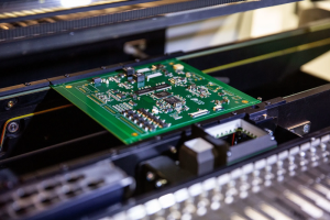
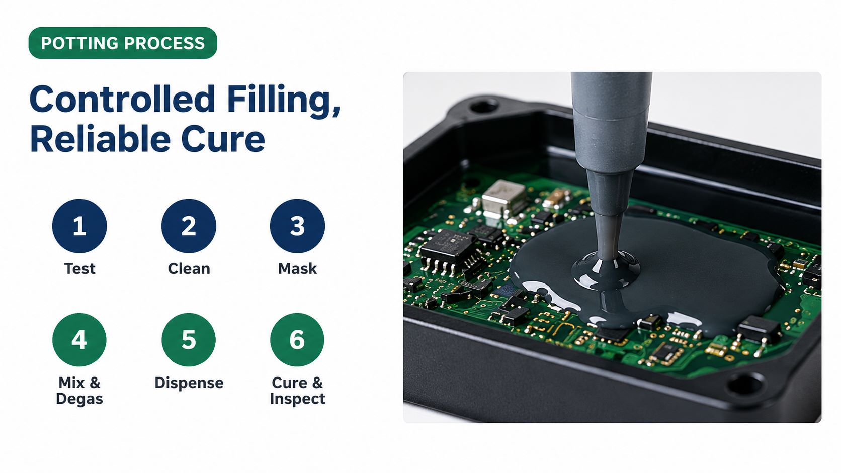
- Inspect the PCBA: Check component orientation, soldering quality, connector placement, polarity, and visible contamination.
- Program and test the assembly: Complete firmware programming, power-on checks, current measurement, communication testing, and functional verification.
- Clean and dry the board: Remove flux, dust, oil, cleaning residue, and moisture that could weaken adhesion or become trapped beneath the compound.
- Mask critical areas: Protect connectors, switches, screw holes, LEDs, test points, vents, adjustment devices, and heat-transfer surfaces.
- Prepare the material: Confirm shelf life, storage conditions, material temperature, mixing ratio, and pot life.
- Mix and degas: Mix the resin carefully to avoid introducing excessive air. Vacuum degassing may be used when required by the material, board geometry, or insulation specification.
- Dispense the compound: Fill from a controlled location and provide an escape path for displaced air.
- Allow settling and bubble release: The resin needs time to flow beneath components and into narrow spaces.
- Cure to the specified profile: Follow the recommended time and temperature. A hard surface does not always mean the material is fully cured internally.
- Inspect and retest: Verify fill height, masking, overflow, cure condition, appearance, and electrical operation.
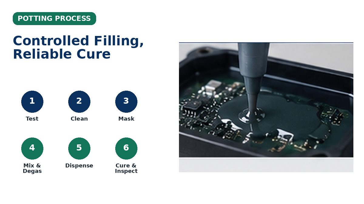
Complex assemblies may require staged filling. This can reduce trapped air, control exotherm, and allow the resin to reach restricted spaces before additional material is added.
What PCB Design and DFM Rules Should Be Set Before Encapsulation?
Encapsulation should be reviewed during PCB and enclosure design rather than added after the assembly is complete.
Important DFM points include:
- Keep connectors, test points, switches, and adjustment devices outside the fill area.
- Leave enough clearance around tall components for resin flow.
- Avoid closed air pockets under transformers, relays, shields, and capacitors.
- Define the fill point, vent path, target fill height, and leakage barriers.
- Review compatibility with solder mask, labels, wire insulation, gaskets, and enclosure plastics.
- Confirm the cure-temperature limits of sensors, batteries, displays, and connectors.
- Keep heat sinks and thermal-interface surfaces free from unwanted resin.
- Review stress around BGAs, QFNs, ceramic capacitors, and large solder joints.
- Define how failed units will be repaired, analyzed, or scrapped.
- Complete programming and functional testing before critical areas become inaccessible.
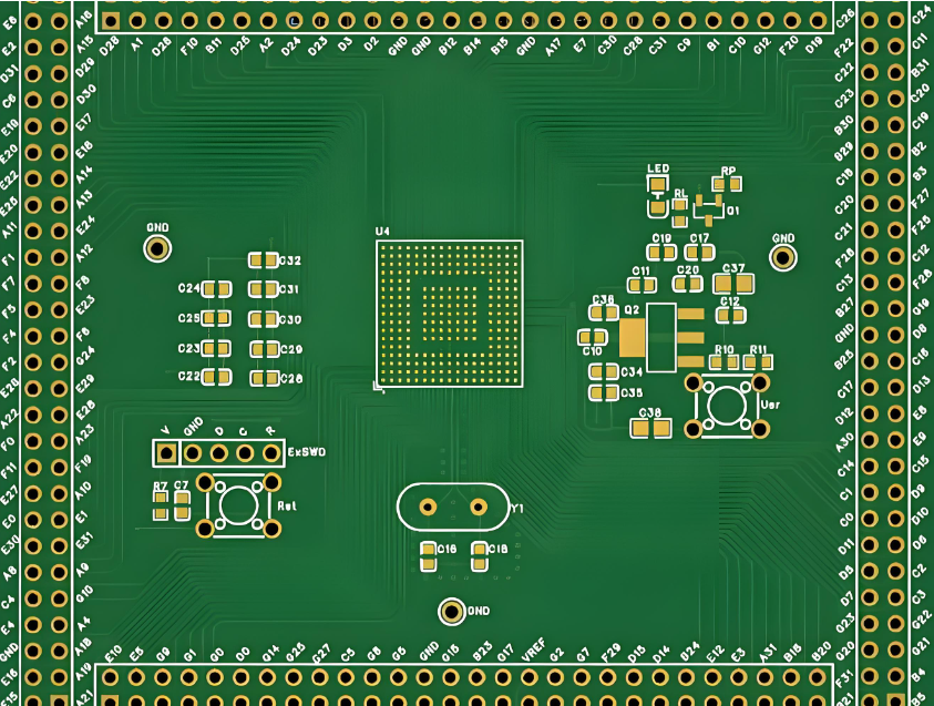
The design package should clearly identify:
- Potting area
- Keep-out zones
- Masking boundaries
- Target fill height
- Resin specification
- Enclosure dimensions
- Fill and vent locations
- Test requirements
- Acceptance criteria
Resin flow should be treated as a mechanical design issue. A narrow gap, tall component, shield can, or enclosed cavity can block flow and trap air. The enclosure drawing and PCB layout should therefore be reviewed together.
What Encapsulation Defects Occur, and How Are They Prevented?
Most PCB encapsulation defects are related to material handling, surface preparation, assembly geometry, dispensing control, or curing conditions.
| Defect | Likely cause | Prevention |
| Air bubbles | Fast mixing or dispensing | Slow mixing, degassing, and controlled filling |
| Internal voids | Poor venting or blocked resin flow | Review fill points, vents, and component spacing |
| Poor adhesion | Flux, oil, dust, or moisture | Clean and dry the PCBA |
| Incomplete curing | Incorrect ratio or low temperature | Control material ratio and cure profile |
| Cracking | High shrinkage or CTE mismatch | Use a more compliant material or staged cure |
| Resin overflow | Unsealed gaps or excess material | Seal openings and control fill volume |
| Thermal hot spots | Weak heat-transfer path | Validate the resin, enclosure, and heat sink together |
| Component damage | High exotherm or excessive rigidity | Select suitable chemistry and cure conditions |
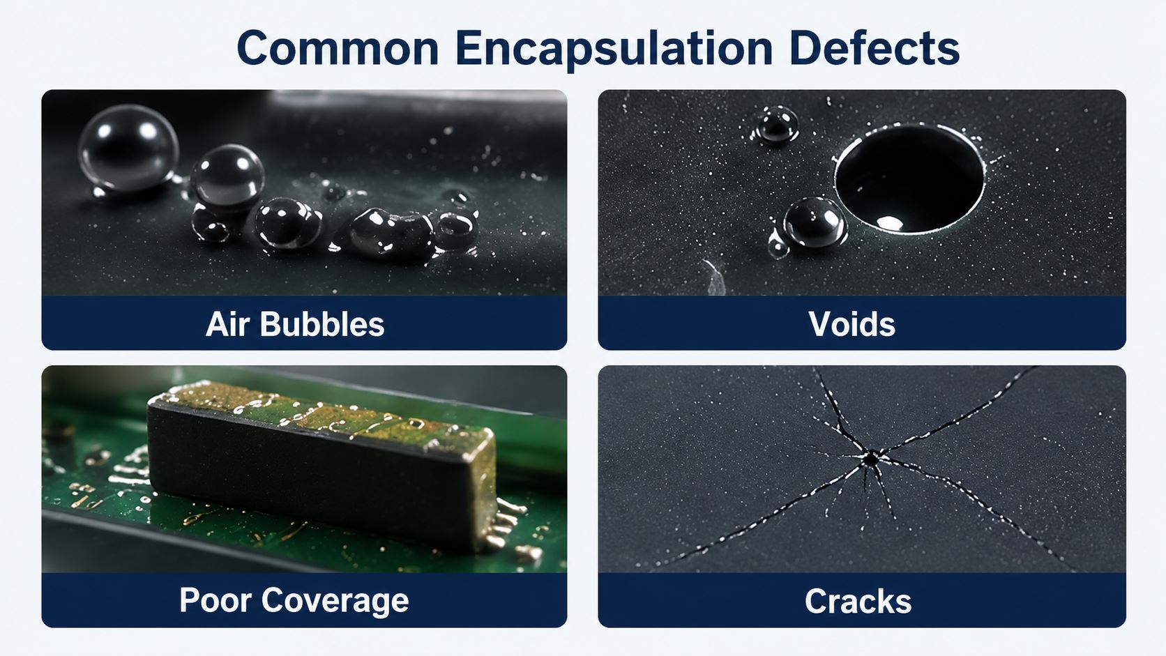
Defect acceptance should match the electrical and environmental risk. A small surface bubble may be cosmetic, while a void between high-voltage conductors can reduce dielectric reliability.
Prototype builds can reveal hidden flow problems before volume production. Depending on the project, validation may include:
- X-ray inspection
- Sample sectioning
- Thermal cycling
- Humidity testing
- Vibration testing
- Dielectric-strength testing
- Destructive analysis
Case Study: FR-4 Potting Dam for Selective Circuit Board Encapsulation
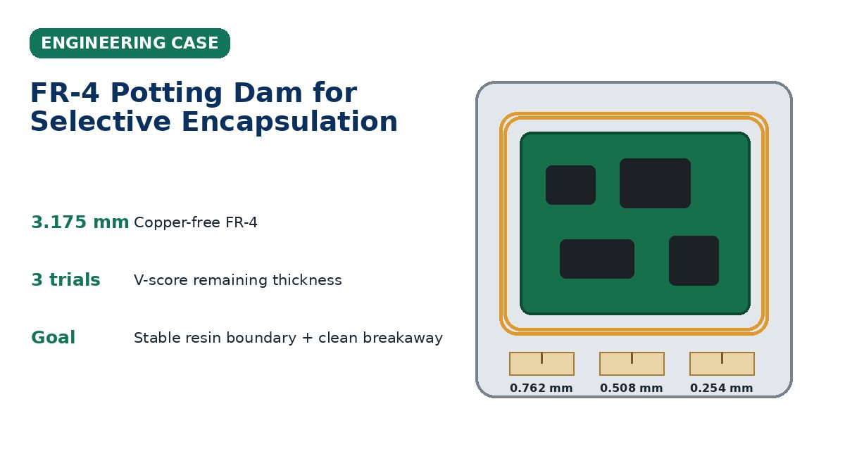
A U.S. customer required a custom FR-4 potting dam to control resin flow during selective circuit board encapsulation.
Project requirements
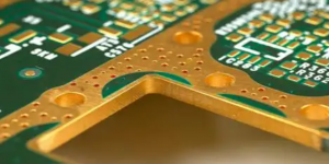
Copper-free FR-4 structure
Board thickness: 3.175 mm
Stable resin boundary
Clean breakaway after potting
No damage to nearby components
The main challenge was balancing dam rigidity with controlled separation. Our engineering team prepared three V-score options with remaining thicknesses of:
- 0.762 mm
- 0.508 mm
- 0.254 mm
- The prototypes allowed the customer to evaluate:
- Dam stability during resin dispensing
- Breakaway force after curing
- Resin overflow control
- Fit with the PCB and enclosure
The project showed that circuit board encapsulation is not only a material-selection task. Potting dams, masking boundaries, fill direction, venting, resin height, and pre-potting testing must be reviewed together.
Best Technology supports encapsulation projects from DFM review and prototype validation through PCB assembly, controlled dispensing, testing, and volume production.
How Are Encapsulated PCBAs Tested, Inspected, and Quoted?
Testing should be divided into pre-potting and post-potting stages.
Before encapsulation
Complete inspections that will become difficult after curing:
- AOI
- X-ray for hidden solder joints when required
- Firmware programming
- Power-on testing
- Current-consumption checks
- Communication and I/O testing
- Connector and polarity verification
- Functional testing
After encapsulation
Final inspection may include:
- Fill-level and coverage checks
- Masking and keep-out verification
- Cure-state inspection
- Surface bubble and overflow review
- Electrical insulation testing
- Final functional testing
- Thermal, humidity, vibration, or burn-in testing
- Lot and material traceability
- A complete RFQ for PCB encapsulation services should include:
- Gerber files
- BOM
- CPL or pick-and-place file
- Assembly drawing
- Enclosure drawing
- Potting area and target fill height
- Masking requirements
- Preferred material or required properties
- Operating temperature
- Moisture and chemical exposure
- Voltage and thermal requirements
- Test specification
- Prototype and production quantity
When the resin has not yet been selected, provide the operating conditions and reliability requirements. The manufacturer can then compare epoxy, silicone, polyurethane, or gel options and validate the process through a pilot build.
FAQs About Circuit Board Encapsulation
Is circuit board encapsulation the same as PCB potting?
Not exactly. Encapsulation is the broader term for surrounding a PCB, PCBA, or component with protective material. Potting is a common encapsulation method in which the compound fills an enclosure or cavity.
Is an encapsulated circuit board waterproof?
It can provide strong moisture protection, but waterproof performance depends on complete coverage, connector sealing, cable entries, enclosure design, material selection, and cure quality.
Which material is best for circuit board encapsulation?
Epoxy is suitable when hardness, adhesion, and chemical resistance are priorities. Silicone performs well under thermal cycling and wide temperature ranges. Polyurethane provides a practical balance of moisture resistance and flexibility.
Can an encapsulated circuit board be repaired?
Some assemblies can be repaired when softer compounds or selective encapsulation are used. Full epoxy potting is usually difficult and time-consuming to remove.
How are bubbles prevented during PCB potting?
Manufacturers control material temperature, mixing speed, resin ratio, vacuum degassing, fill direction, dispensing rate, venting, and settling time.
Does potting compound improve heat dissipation?
A thermally conductive compound can improve heat transfer when it forms a continuous path to an enclosure or heat sink. It cannot compensate for an inadequate thermal design.
Finally, turn your encapsulation design into a production-ready PCBA. Best Technology supports PCB fabrication, component sourcing, PCBA assembly, programming, functional testing, conformal coating, and circuit board encapsulation for prototypes, small batches, and volume production. Send your Gerber files, BOM, assembly drawing, enclosure details, potting area, operating environment, and test requirements to sales@bestpcbs.com. Our engineering team will review the encapsulant options, masking boundaries, resin flow, thermal risks, DFM issues, and inspection plan before production-helping you reduce trial builds, avoid potting defects, and move into production with fewer revisions.