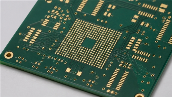
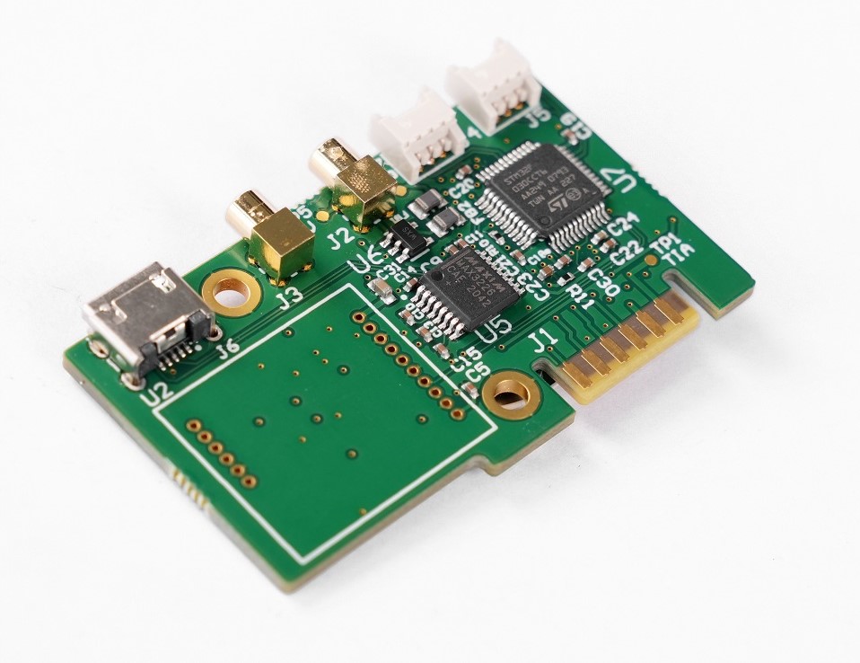
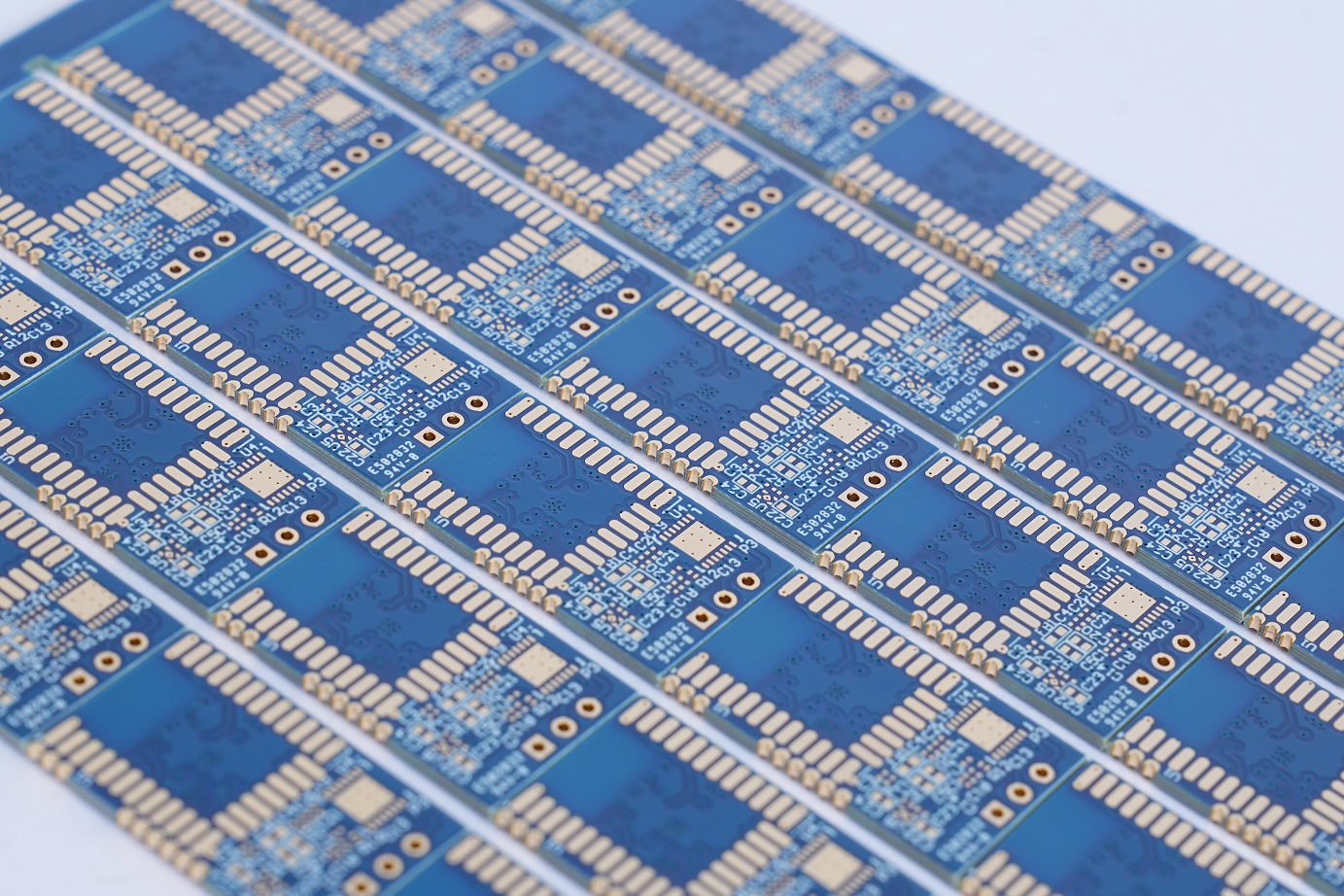
ENIG is a two-layer PCB surface finish in which electroless nickel is deposited over exposed copper and a thin immersion-gold layer protects the nickel until assembly. The finish creates flat, solderable pads that suit fine-pitch SMT, BGA, QFN, and many mixed-technology boards.
ENIG is not automatically the best finish for every design. Its value depends on pad geometry, storage and assembly plans, wear requirements, signal frequency, cost targets, and how well the plating process is controlled. This guide explains the layer structure, ENIG plating process, thickness requirements, black pad risk, inspection methods, and the decisions that should appear on a fabrication drawing.
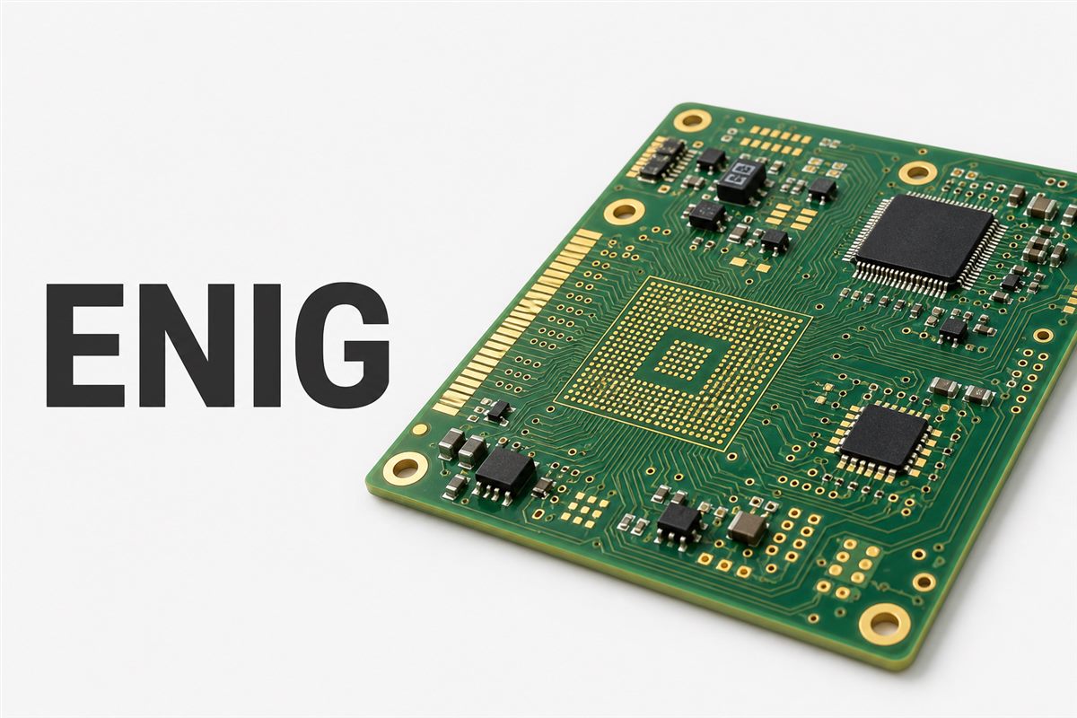
What Is ENIG in PCB Manufacturing?
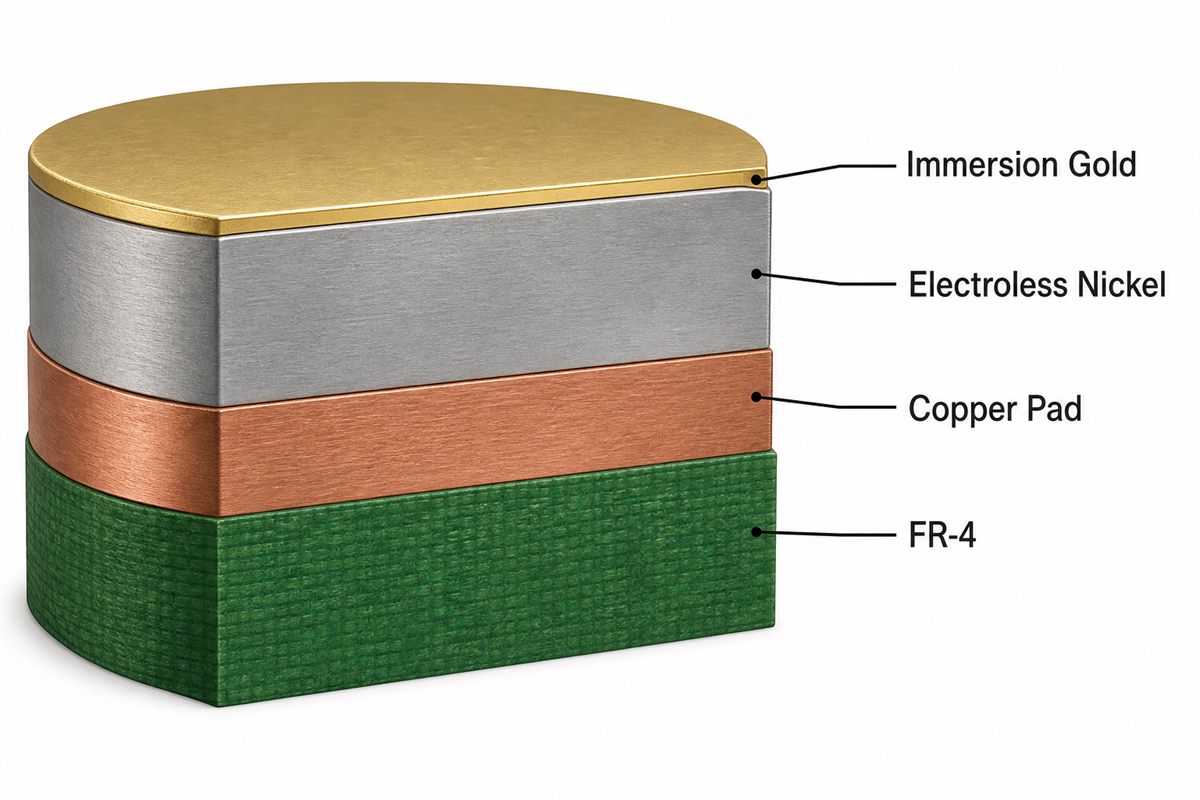
ENIG means Electroless Nickel Immersion Gold, a chemically deposited finish that protects exposed copper and provides a flat surface for soldering. The nickel layer is the functional barrier and solderable surface; the much thinner gold layer mainly prevents the nickel from oxidizing before assembly.
| ENIG Element | Main Function | Engineering Meaning |
| Immersion gold | Protects nickel during storage and handling | Dissolves into solder during reflow; it is not a wear-resistant hard-gold layer |
| Electroless nickel | Provides the solderable barrier over copper | Controls joint-interface behavior and can affect high-frequency conductor loss |
| Copper pad | Carries current and anchors the plated finish | Cleaning and micro-etch quality affect adhesion and uniform deposition |
The word “gold” can be misleading. ENIG does not place a thick, mechanically durable gold layer on the board. Edge connectors, sliding contacts, or repeated insertion surfaces normally need an electrolytic hard-gold specification rather than immersion gold.
How Does ENIG Plating Work?
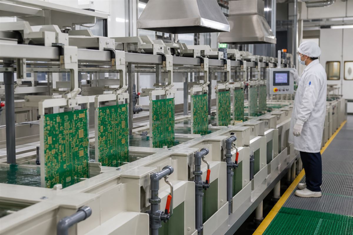
ENIG plating uses controlled chemical reactions rather than external plating current, so isolated pads can receive a uniform finish without electrical bus bars. A typical production sequence includes:
- Clean and condition the copper: Remove oil, oxide, fingerprints, and residues that could interrupt deposition.
- Micro-etch: Expose a fresh, controlled copper surface for activation and adhesion.
- Activate the surface: Establish catalytic sites so electroless nickel can initiate consistently.
- Deposit electroless nickel: Build the nickel-phosphorus barrier to the specified thickness.
- Apply immersion gold: Replace a small amount of surface nickel with gold through a displacement reaction.
- Rinse and dry: Remove chemistry without leaving ionic residue or water marks.
- Inspect and measure: Check appearance, coverage, thickness, and any project-specific acceptance requirements.
Bath chemistry, temperature, pH, dwell time, loading, solution movement, rinsing, and maintenance all affect the result. A board can look uniformly gold while still carrying an interface problem, so appearance is only one part of acceptance.
What ENIG Thickness Should Be Specified?
ENIG thickness should be stated by layer and tied to an agreed standard or drawing requirement. Public IPC material for IPC-4552 identifies 3–6 µm (118.1–236.2 µin) for electroless nickel. The immersion-gold deposit is much thinner; the 2012 amendment discussed a 0.04 µm (1.6 µin) lower limit with additional process and measurement restrictions, while 0.05 µm (about 2 µin) is a common minimum reference.
| Layer | Common Reference | Purpose |
| Electroless nickel | 3–6 µm (118.1–236.2 µin) | Copper diffusion barrier and solderable interface |
| Immersion gold | Drawing- and standard-controlled; commonly around 0.05–0.10 µm | Temporary oxidation protection for nickel |
Do not copy a thickness range without identifying the applicable revision and procurement conditions. The project drawing remains the controlling document. Our detailed IPC-4552 ENIG specification guide explains why the revision, measurement pad, statistical requirement, and acceptance language matter.
Thicker gold is not automatically better. A longer immersion reaction can increase nickel attack, while insufficient coverage can leave the nickel vulnerable during storage. The correct target is a stable, qualified process that meets the specified deposit requirement.
What Are the Advantages of an ENIG Surface Finish?
An ENIG surface finish is most valuable when flatness, solderability, storage protection, and isolated-pad coverage matter more than the lowest bare-board cost. Its main advantages are:
- Flat pads: The chemical deposit does not create the solder domes associated with HASL, which helps fine-pitch printing and placement.
- Fine-pitch compatibility: BGA, QFN, CSP, and small passive pads benefit from controlled coplanarity.
- Lead-free assembly compatibility: A properly controlled finish supports common lead-free reflow processes.
- Coverage of isolated features: Electroless deposition does not require every pad to connect to a plating bus.
- Storage protection: The gold protects nickel from oxidation before assembly when packaging and storage remain controlled.
- Useful contact performance: ENIG can suit low-wear contact surfaces, test pads, and membrane-switch contacts when the application is qualified.
These benefits are conditional. ENIG does not replace hard gold for abrasive contacts, and it does not remove the need to control stencil design, solder paste, reflow, storage, and handling.
What Causes ENIG Black Pad?
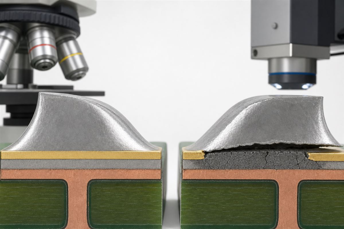
ENIG black pad is associated with excessive or abnormal corrosion of the electroless-nickel surface during immersion-gold deposition. The affected interface can become phosphorus-rich and brittle, allowing a solder joint to fracture at or near the nickel surface even when the exposed pad originally looked gold.
Risk rises when the process allows aggressive nickel attack or uneven exchange. Contributing conditions can include:
- unstable or poorly maintained nickel and gold baths;
- excessive immersion time or an overly aggressive gold reaction;
- uncontrolled nickel-phosphorus composition;
- poor copper preparation, contamination, or uneven activation;
- local chemistry stagnation around small or restricted features;
- weak process monitoring and incomplete failure analysis.
Prevention depends on process control, not visual sorting alone. Thickness measurement, bath records, qualified process windows, solderability testing, and corrosion evaluation provide different pieces of evidence. For high-consequence applications, the drawing and quality plan should define which records or tests are required.
How Is ENIG Inspected and Accepted?
ENIG acceptance combines visual inspection, deposit measurement, and project-specific functional evidence. No single test proves every quality attribute.
- Visual inspection: Finds exposed copper, skips, stains, contamination, handling damage, and obvious non-uniformity.
- XRF measurement: Measures nickel and gold deposit thickness at defined locations without destroying the board.
- Solderability testing: Evaluates whether the surface wets under the selected test method and conditioning.
- Adhesion checks: Detect plating separation or weak interfaces under the specified method.
- Cross-section or stripped-gold analysis: Supports deeper investigation of nickel corrosion and interface morphology.
- Assembly evidence: Reflow, joint inspection, shear or pull testing, and product-level qualification may be needed when the application is demanding.
An XRF report is valuable because it confirms thickness at measured points, but it does not by itself prove solderability, corrosion severity, cleanliness, or final joint reliability. The acceptance plan should match the actual failure risk.
ENIG vs HASL
ENIG vs HASL is mainly a trade-off between flatness and process cost. ENIG normally provides flatter pads for fine-pitch assembly, while lead-free HASL is often more economical for designs that tolerate coating variation.
| Decision Point | ENIG | Lead-Free HASL |
| Pad flatness | Very flat chemical deposit | More thickness variation from solder leveling |
| Fine-pitch assembly | Usually preferred for BGA, QFN, and dense SMT | Better suited to less demanding pad geometries |
| Thermal exposure during finishing | Lower-temperature chemical process | Board contacts molten solder during finishing |
| Main process risk | Nickel corrosion and black pad if poorly controlled | Uneven coating and thermal stress |
| Relative bare-board cost | Usually higher | Usually lower |
Our separate HASL lead-free vs ENIG comparison provides more detail for projects choosing between these two finishes.
ENIG vs ENEPIG
ENIG vs ENEPIG differs mainly because ENEPIG adds an electroless-palladium layer between nickel and immersion gold. That palladium barrier broadens bonding options and separates the immersion-gold reaction from the nickel surface, but it adds chemistry, process control, and cost.
| Item | ENIG | ENEPIG |
| Layer structure | Nickel + immersion gold | Nickel + palladium + immersion gold |
| Typical selection reason | Flat solderable finish for general fine-pitch assembly | Soldering plus broader wire-bonding or interface requirements |
| Black pad pathway | Direct gold-on-nickel displacement requires tight control | Palladium separates nickel from the immersion-gold reaction |
| Relative process cost | Lower | Higher |
ENEPIG should not be selected merely because it has one more metal layer. The application needs to justify the added finish. See our ENIG vs ENEPIG manufacturing comparison for additional process context.
When Should You Choose an ENIG PCB?
Choose an ENIG PCB when the design needs flat solderable pads and the assembly, storage, electrical, and wear conditions fit the finish. ENIG is often a strong candidate for:
- BGA, QFN, CSP, and fine-pitch SMT land patterns;
- HDI or via-in-pad structures that require controlled coplanarity;
- mixed SMT and through-hole assemblies;
- boards with isolated pads that cannot use electrolytic plating connections;
- projects needing better pre-assembly oxidation protection than a bare copper surface;
- low-wear contacts that have been qualified for the actual mechanical cycle.
Consider another finish when repeated contact wear, very low cost, aggressive wire bonding, or ultra-low-loss RF performance dominates the decision. Rogers data shows that nickel-bearing ENIG can add conductor loss, especially in thin microstrip or tightly coupled coplanar structures at microwave and millimeter-wave frequencies. In such cases, compare immersion silver, OSP, selective finishing, or another qualified low-loss finish rather than assuming ENIG is harmless.
How Should ENIG Be Specified on a Fabrication Drawing?
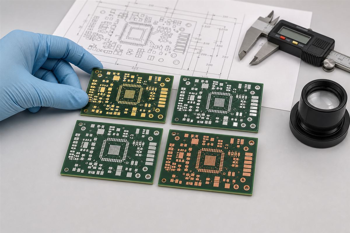
An ENIG fabrication note should identify the finish, governing specification, revision, deposit requirement, and any special inspection or application need. Writing only “gold finish” is ambiguous because it does not distinguish ENIG from ENEPIG, hard gold, soft electrolytic gold, or another nickel/gold system.
A practical drawing package should make the following clear:
- surface finish: Electroless Nickel Immersion Gold (ENIG);
- applicable IPC-4552 revision or customer-controlled specification;
- nickel and gold requirements, including any permitted exception;
- measurement method, coupon or pad requirements, and reporting expectations;
- whether pads are for soldering, low-wear contact, wire bonding, RF traces, or another special function;
- selective hard gold, ENEPIG, OSP, or other mixed-finish areas if required;
- storage, packaging, solderability, cleanliness, or qualification requirements that exceed normal purchase acceptance.
Include the finish requirement in the fabrication drawing or controlled notes, not only in an email or quotation comment. The Gerber data shows exposed copper geometry, but it does not define the complete finish acceptance requirement.
What Affects ENIG Cost and Lead Time?
ENIG usually costs more than HASL or OSP because it adds controlled chemical processing, precious-metal consumption, bath maintenance, measurement, and inspection. The finish may also affect lead time when the board needs unusual thickness, selective finishes, special coupons, additional testing, or project-specific documentation.
- Gold requirement: A nonstandard deposit target can change chemistry time and cost.
- Panel design and exposed area: Total plateable area affects process loading and material consumption.
- Mixed finishes: ENIG combined with hard gold or OSP adds masking and process steps.
- Testing and reports: XRF maps, solderability tests, cross-sections, or extra coupons require planning.
- Special applications: Wire bonding, RF conductors, contacts, and high-reliability products need more review than a standard solder-only finish.
- Storage and packaging: Long storage windows or controlled packaging requirements may add handling and documentation.
For a useful quotation, provide the Gerber or ODB++ data, fabrication drawing, stackup, board quantity, panel requirements, finish specification, and any assembly or test expectations. This allows finish cost to be evaluated with the whole build rather than as an isolated checkbox.
FAQ About ENIG PCB
What is the ENIG PCB full form?
ENIG stands for Electroless Nickel Immersion Gold. It is a two-layer metallic finish applied over exposed PCB copper: electroless nickel forms the barrier and solderable surface, while immersion gold protects the nickel before assembly.
Is ENIG real gold?
Yes, the top deposit is gold, but it is extremely thin and is produced by an immersion displacement reaction. ENIG should not be confused with thick electrolytic hard gold used for wear-resistant edge contacts.
Does ENIG contain nickel?
Yes. Nickel is the main functional layer between copper and gold. It provides the solderable barrier, but its chemistry must be controlled to reduce corrosion risk, and it can add loss to some high-frequency transmission lines.
Can ENIG be used for gold fingers?
ENIG may suit low-wear contacts, but repeated insertion edge fingers normally require electrolytic hard gold with a specified nickel underplate and wear thickness. The mechanical cycle and contact force should determine the finish.
What is ENIG PCB finish shelf life?
ENIG PCB finish shelf life depends on deposit quality, cleanliness, packaging, humidity, temperature, handling, and the customer’s assembly standard. Do not assume a universal storage period; confirm the supplier’s controlled storage condition and requalification rule.
Can ENIG be soldered more than once?
ENIG is commonly used on double-sided assemblies that undergo more than one thermal cycle. The acceptable number of reflows depends on laminate, component, solder paste, profile, pad design, storage history, and the product qualification plan.
Is ENIG suitable for wire bonding?
ENIG can support some bonding applications, but suitability depends on wire material, bond method, deposit condition, and the specified process. ENEPIG or another finish may be more appropriate when wire bonding is a primary requirement.
Does XRF detect ENIG black pad?
XRF measures nickel and gold thickness, not the complete condition of the buried nickel surface. It supports process control but cannot alone rule out hyper-corrosion, contamination, poor solderability, or a brittle interface.
Is ENIG suitable for RF PCBs?
ENIG can work in many RF boards, but the nickel layer can increase conductor loss and phase variation as frequency, current concentration, and finish sensitivity rise. Microwave and mmWave designs should compare finishes using the actual transmission-line geometry and loss budget.
What files are needed to quote an ENIG PCB?
Send Gerber or ODB++ data, drill files, fabrication drawing, stackup, dimensions, quantity, finish specification, and any coupon, XRF, solderability, assembly, or packaging requirements. Include BOM and placement data when PCBA is also required.
How Can EBest Circuit Support Your ENIG PCB Project?
At EBest Circuit, we review the finish together with the PCB structure, exposed-pad geometry, component pitch, assembly plan, test requirements, and end-use conditions. We can support PCB fabrication and PCBA projects that specify ENIG, while confirming nonstandard thickness, selective finishes, reporting, and special reliability requirements before production.
Send your Gerber files, fabrication drawing, stackup, quantity, ENIG requirement, and any assembly or inspection notes to sales@bestpcbs.com. Our engineering team will review the data and help confirm whether ENIG PCB finish fits the project or whether another surface finish should be evaluated. You can also review our FR4 PCB manufacturing process when planning the full bare-board build.