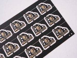
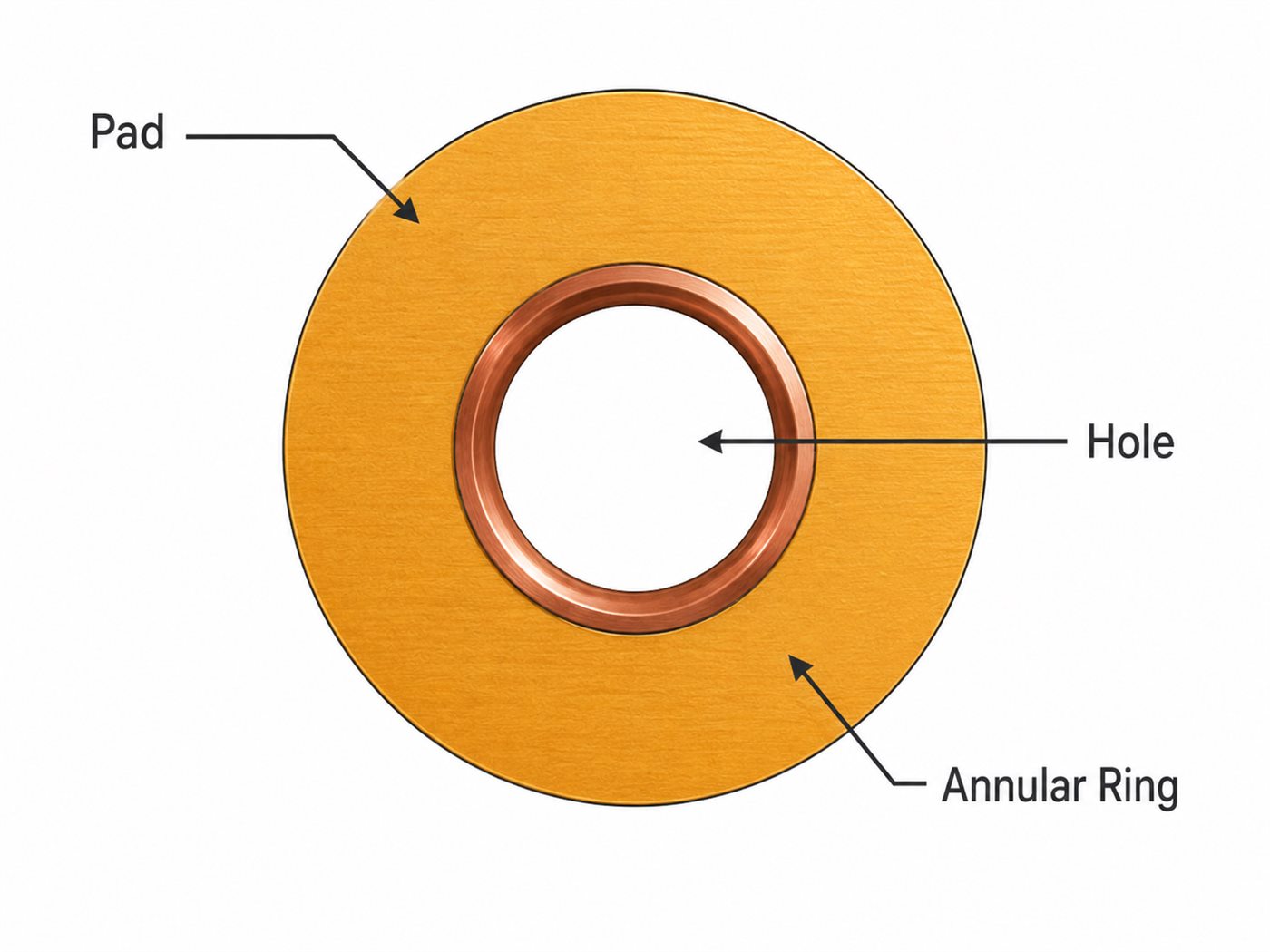
A PCB annular ring is the copper area that remains around a drilled hole. It appears on vias and plated through-holes as the circular copper border between the hole edge and the outer edge of the pad.
The basic formula is simple:
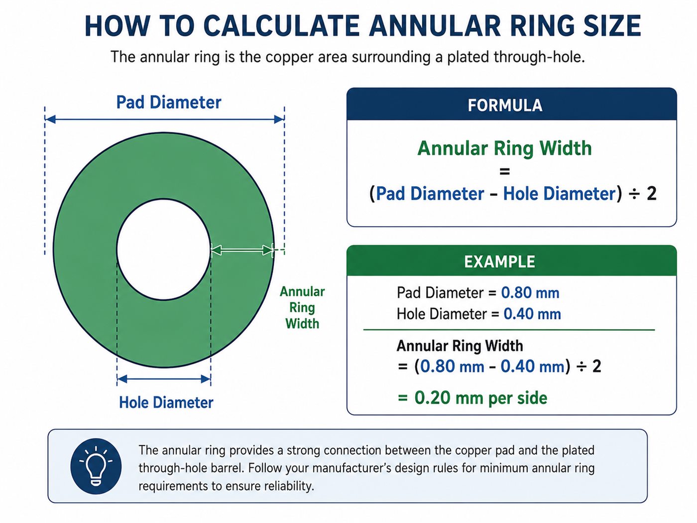
Annular ring width = (pad diameter − hole diameter) ÷ 2
That result is only the nominal design value. On a finished board, the narrowest part of the ring can be smaller because of drill movement, layer misregistration, etching variation, material movement, and hole-size tolerance.
This guide explains how annular rings are calculated, how they differ across PCB via types, what affects the minimum size, and how designers can prevent tangency and breakout before fabrication.

What Is an Annular Ring in PCB Design?
An annular ring is the copper land surrounding a drilled or laser-formed hole on a PCB layer. It can appear around:
- Through vias
- Blind vias
- Buried vias
- Laser microvias
- Plated through-holes for components
The ring is not a separate part. It is simply the copper left between the hole and the edge of the pad.
For example, a via with a 0.60 mm pad and a 0.30 mm hole has a nominal annular ring of 0.15 mm:
(0.60 mm − 0.30 mm) ÷ 2 = 0.15 mm
This calculation assumes the hole is centered. In production, the actual ring should be judged at its narrowest point.
A through via may also have more than one annular ring: one on the top layer, one on the bottom layer, and additional rings on connected inner layers.
Why Is the PCB Annular Ring Important?
The annular ring supports both electrical continuity and manufacturing reliability.
Its main functions are to:
- Connect the plated barrel to traces or copper planes
- Provide room for normal drill and registration variation
- Maintain continuity when the hole is slightly off-center
- Support soldering around plated component holes
- Improve the mechanical strength of pads used for connectors, headers, switches, and terminals
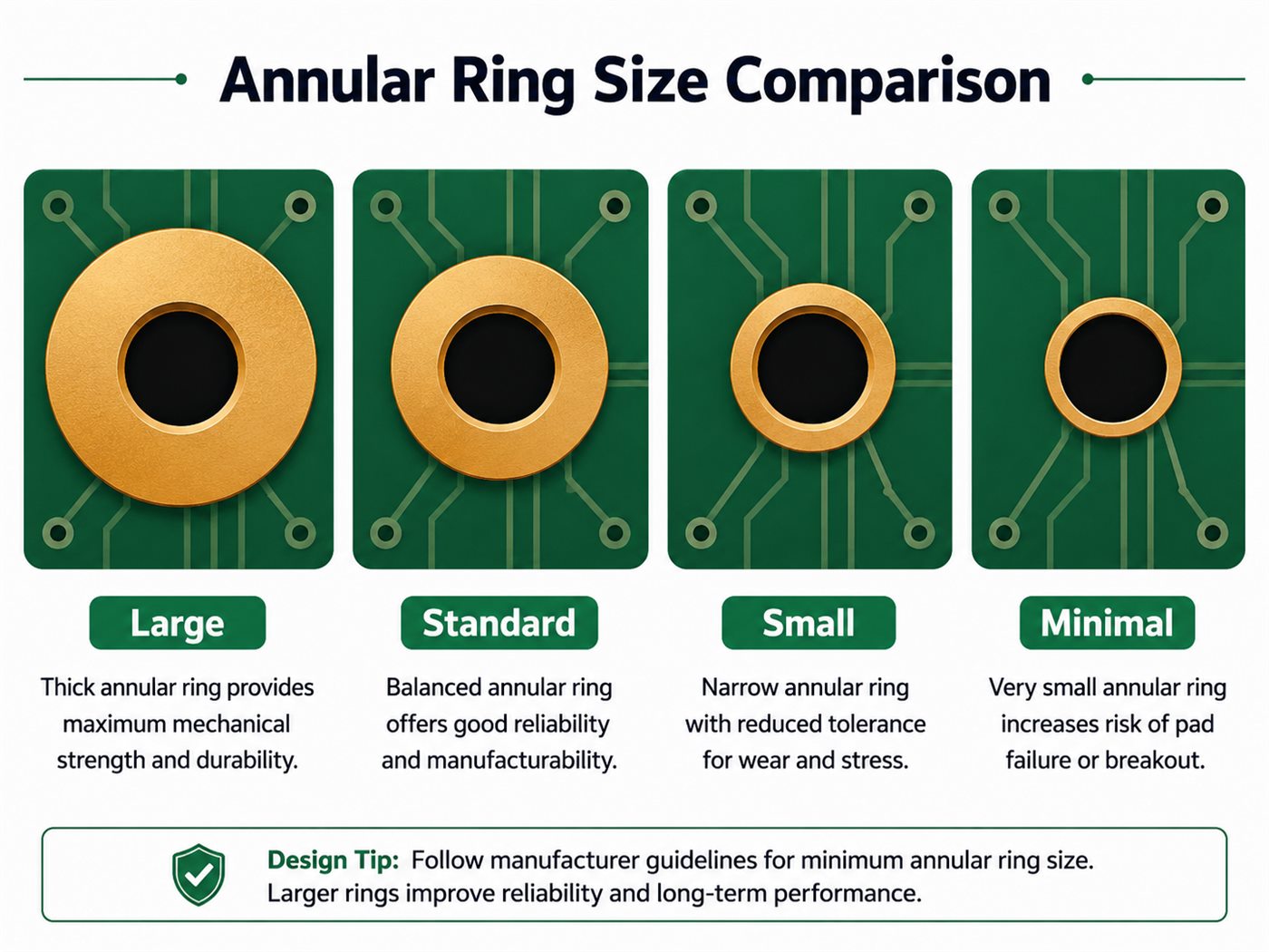
A narrow ring is not always a defect. Fine-pitch and HDI designs often use small lands on purpose. The problem begins when the designed ring leaves less margin than the fabrication process can reliably maintain.
A practical annular ring should therefore balance two competing needs:
- Smaller pads improve routing density.
- Larger pads provide more manufacturing margin.
The right value is not the largest possible ring. It is the smallest geometry that still matches the selected PCB process.
Annular Ring vs Via, Pad, and Plated Through-Hole
These terms are related, but they are not interchangeable.
| Term | Meaning | Main function |
|---|---|---|
| Via | A conductive hole connecting selected PCB layers | Provides vertical electrical connection |
| Pad or land | Copper surrounding a hole or component terminal | Connects the hole to traces, planes, or solder |
| Annular ring | Copper remaining between the hole edge and pad edge | Maintains copper continuity around the hole |
| Plated through-hole | A plated hole passing through the full board | Connects layers or accepts a component lead |
| Via barrel | Copper plating on the hole wall | Carries current between layers |
| Antipad | Clearance around a hole in an unconnected plane | Prevents unwanted electrical contact |
| Finished hole | Final opening after plating and processing | Controls component fit or final via size |
The via is the complete interconnection structure. The annular ring is only the copper surrounding that hole on a particular layer.
How Do You Calculate Annular Ring Size?
For a centered circular pad and hole, use:
Annular ring width = (pad diameter − hole diameter) ÷ 2
Example in Millimeters
- Pad diameter: 0.80 mm
- Hole diameter: 0.40 mm
- Annular ring: 0.20 mm
Example in Mils
- Pad diameter: 24 mil
- Hole diameter: 12 mil
- Annular ring: 6 mil
The same logic applies to most round vias. For oval or irregular pads, measure the shortest distance between the hole edge and the nearest pad boundary.
Before calculating, confirm which hole value is being used:
- Drill tool diameter: the nominal drill selected by the fabricator
- Drilled hole diameter: the opening before copper plating
- Finished hole diameter: the final usable hole after plating
These values are not always the same. For a plated component hole, the finished hole controls lead fit. The manufacturer normally drills a larger opening so the final plated hole reaches the required size.
For design review, always label the hole value clearly. Mixing drill size and finished-hole size can produce an annular ring that looks correct in CAD but fails manufacturing review.
How Do You Calculate the Required Pad Diameter?
If the hole size and target ring width are known, reverse the formula:
Pad diameter = hole diameter + 2 × target annular ring
For a 0.30 mm hole and a target ring of 0.15 mm:
Pad diameter = 0.30 + 2 × 0.15 = 0.60 mm
This gives the nominal CAD pad diameter. A production design may still need extra allowance for:
- Drill-position tolerance
- Inner-layer registration
- Material expansion and contraction
- Etching variation
- Copper plating
- Finished-hole tolerance
- Board thickness and layer count
- IPC class or customer-specific requirements
A more practical relationship is:
Required pad diameter = reference hole diameter + 2 × required finished ring + manufacturing allowance
The allowance should come from the intended PCB manufacturer. A standard four-layer board, a thick-copper board, and a high-layer-count HDI board may require different land sizes even when the hole diameter is identical.
PCB Annular Ring Size Chart for Vias and PTHs
The table below complements a broader standard PCB via sizes reference and shows nominal geometry only. It should not be treated as a universal fabrication capability chart.
| Hole diameter | Pad diameter | Nominal annular ring |
|---|---|---|
| 0.20 mm | 0.40 mm | 0.10 mm |
| 0.20 mm | 0.45 mm | 0.125 mm |
| 0.25 mm | 0.50 mm | 0.125 mm |
| 0.30 mm | 0.60 mm | 0.15 mm |
| 0.30 mm | 0.70 mm | 0.20 mm |
| 0.40 mm | 0.80 mm | 0.20 mm |
| 0.60 mm | 1.00 mm | 0.20 mm |
| 0.80 mm | 1.30 mm | 0.25 mm |
| 1.00 mm | 1.60 mm | 0.30 mm |
A 0.20 mm hole inside a 0.40 mm pad creates a nominal 0.10 mm ring. If the hole shifts 0.05 mm toward one side, the narrowest ring becomes about 0.05 mm.
That is why the nominal number alone is not enough. Finished results also depend on:
- Drill accuracy
- Layer count
- Board thickness
- Copper weight
- Panel size
- Material stability
- Registration capability
For release to production, replace generic numbers with the actual capability values of the selected factory.
What Is the Minimum Annular Ring for a PCB?
A PCB minimum annular ring rule must account for the selected drilling process and factory capability; there is no single minimum annular ring for every PCB.
The appropriate value depends on:
- Mechanical or laser drilling
- Board thickness
- Layer count
- Copper weight
- Via type
- Material system
- Product class
- Factory capability
Mechanical drills usually require more positional allowance than laser-drilled microvias. Plated component holes may also need larger pads because the land supports both soldering and mechanical stress.
Three different values should be kept separate:
- Designed annular ring: the nominal CAD value
- Process minimum: the smallest value the factory accepts in the design data
- Finished annular ring: the copper left at the narrowest point after fabrication
A factory may require a larger designed ring so the completed board still retains enough copper after drilling and registration variation.
This becomes especially important in:
- BGA fan-out
- Fine-pitch connector areas
- Thick boards
- Heavy-copper PCBs
- High-layer-count boards
- Designs using small mechanical vias
Confirm the minimum pad-to-hole relationship before routing is finalized. Fixing a pad-size problem after the layout is complete usually affects clearances, trace escape paths, and plane spacing.
IPC Annular Ring Requirements for Class 1, Class 2, and Class 3
IPC documents separate design guidance, fabrication performance, and finished-board acceptance.
Commonly referenced standards include:
- IPC-2221 for generic PCB design
- IPC-2222 for rigid-board design
- IPC-2226 for HDI design
- IPC-6012 for rigid-board qualification and performance
- IPC-A-600 for printed-board acceptability
The product class also matters:
- Class 1: general electronic products with limited-life requirements
- Class 2: dedicated-service products where continued performance is expected
- Class 3: high-performance products where failure or downtime may be critical
Annular ring acceptance may vary by:
- Internal or external layer
- Plated-hole type
- Product class
- Standard revision
- Industry addendum
- Customer drawing requirements
Avoid placing a single “IPC minimum annular ring” number on every drawing. Instead, specify the applicable standard, revision, class, and any additional acceptance criteria.
For Class 3 or other high-reliability work, the fabrication drawing should also clarify whether special internal-layer registration, microsection, coupon, or inspection requirements apply.
Inner-Layer vs Outer-Layer Annular Rings
Outer-layer rings are visible on the board surface and can usually be inspected directly.
Inner-layer rings are harder to evaluate. They may require:
- Registration data
- X-ray inspection
- Process coupons
- Microsection analysis
- Controlled quality records
Inner layers are particularly sensitive to movement during imaging, lamination, and drilling. A via can look centered on the outer surface while an internal land sits close to tangency.
Outer layers have their own variables, including copper plating and final etching. For that reason, inner and outer annular rings may use different inspection references.
A multilayer DFM review should compare the drill file against every connected copper layer, not only the top and bottom Gerbers.
Annular Ring Rules for Through Vias, Blind Vias, Buried Vias, and Microvias
Different hole structures need different pad rules.
Through Vias
A PCB via annular ring for a through via must tolerate drill movement across the full board thickness and registration variation among all connected layers. Through vias are usually mechanically drilled after lamination.
Blind Vias
Blind vias connect an outer layer to one or more inner layers. Depending on the stack-up, they may be mechanically drilled or laser formed.
Buried Vias
Buried vias connect inner layers and are fabricated within a laminated subassembly. Their geometry must match the subassembly thickness and sequential-lamination process.
Microvias
Microvias are normally laser drilled and often connect adjacent layers. They can use smaller lands, but the design must still consider:
- Capture and target land size
- Dielectric thickness
- Copper plating quality
- Via filling
- Stacked or staggered construction
- Reliability requirements
Plated Through-Holes
PTH pads must account for component lead size, finished-hole tolerance, soldering, and mechanical loading. A connector or terminal block often needs a wider land than a small signal via.
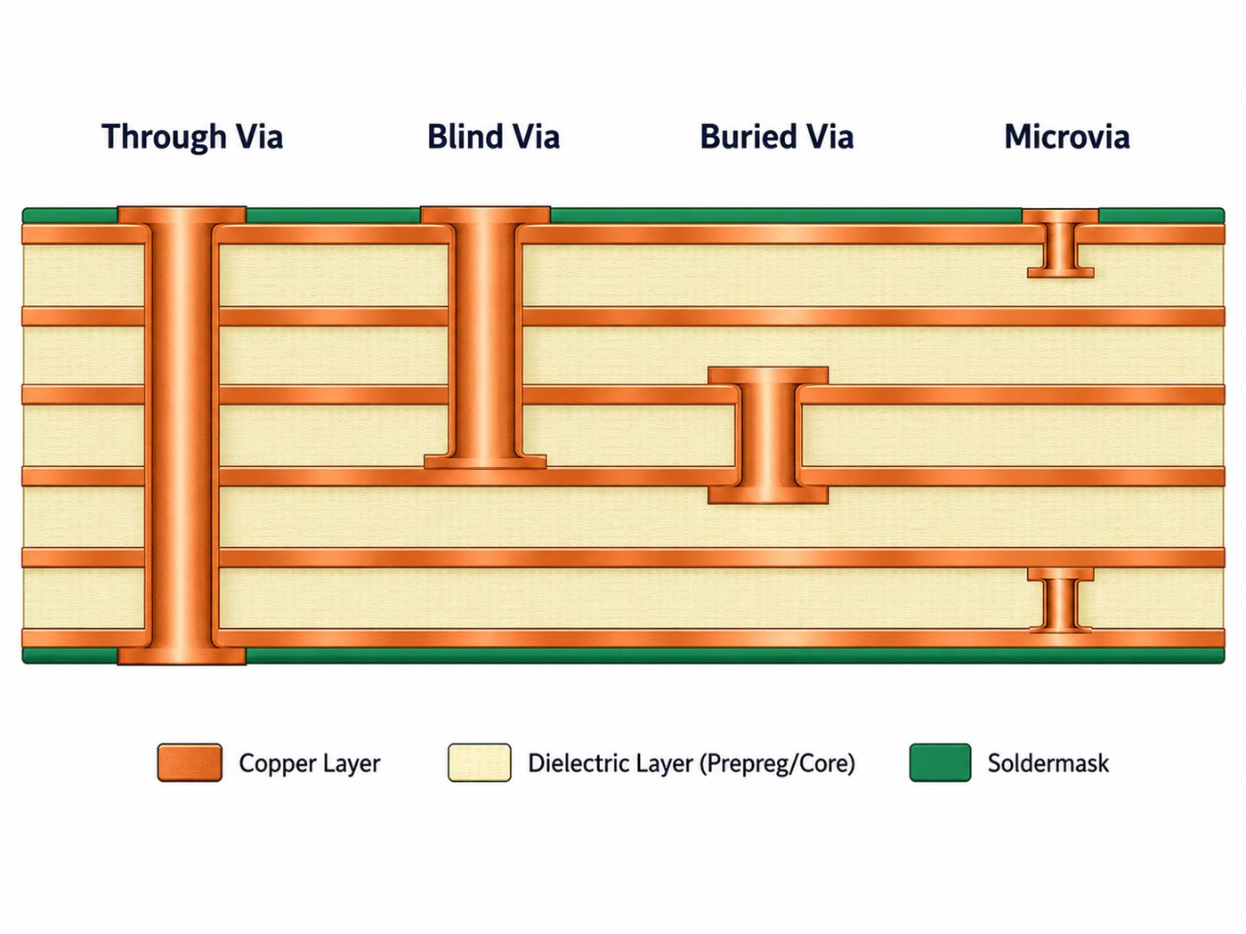
Do not apply one global rule to every hole. Set separate constraints for through vias, microvias, blind or buried vias, and component holes.
How Does Drill Tolerance Cause Tangency, Breakout, and Pad Rupture?
Annular ring quality is judged at the narrowest point around the hole.
Four conditions are common:
- Centered hole: copper is distributed evenly around the opening.
- Reduced ring: the hole is off-center, but copper remains around it.
- Tangency: the hole edge reaches the pad edge.
- Breakout: the hole extends beyond the pad boundary.
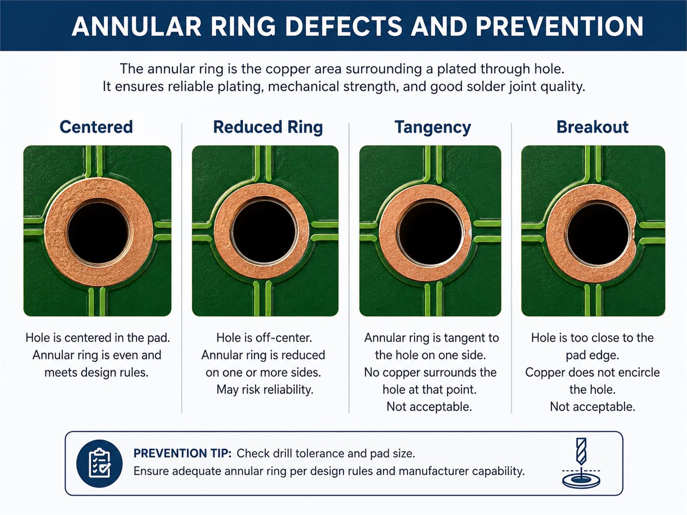
Typical causes include:
- Drill wander
- Layer misregistration
- Pads that are too small
- Incorrect finished-hole assumptions
- Material movement during lamination
- Etching variation
- Incomplete DRC or DFM rules
Designers can reduce the risk by:
- Increasing pad diameter where routing space allows
- Confirming whether hole values are drilled or finished dimensions
- Using separate rules for different via types
- Adding teardrops where narrow traces enter pads
- Checking drill registration on every copper layer
- Stating the required IPC class in the fabrication notes
- Requesting a DFM review before release
Larger pads improve tolerance, but they also consume routing space and increase plane clearance. The practical goal is a stable design, not an oversized one.
FAQs About PCB Annular Rings
What Is the Annular Ring on a PCB?
The annular ring is the copper area between the edge of a drilled hole and the outer edge of its pad. It connects the plated hole wall to traces, planes, or component pads.
How Do You Calculate PCB Annular Ring Width?
For a circular pad and centered hole, subtract the hole diameter from the pad diameter and divide the result by two:
Annular ring = (pad diameter − hole diameter) ÷ 2
What Is the Difference Between a Via and an Annular Ring?
A via is the complete conductive structure used to connect PCB layers. The annular ring is only the copper surrounding the via hole on a particular layer.
What Is the Minimum Annular Ring for a Standard PCB?
There is no universal value. The minimum depends on drill type, board construction, layer count, product class, and factory capability. Use the PCB manufacturer’s published design minimum rather than a generic number.
Can Inner and Outer Layers Use the Same Annular Ring Size?
They can use the same nominal CAD pad size, but their manufacturing and acceptance conditions may differ. Internal layers are especially sensitive to layer registration and lamination movement.
What Causes Annular Ring Breakout?
Breakout occurs when the drilled hole extends beyond the pad edge. Common causes include insufficient pad diameter, drill-position variation, layer misregistration, material movement, and incorrect hole-size assumptions.
Is Annular Ring Measured from the Drilled Hole or Finished Hole?
The reference depends on the layer, hole type, fabrication specification, and inspection requirement. Component-hole design often begins with the finished-hole requirement, while manufacturing calculations may also use the drilled diameter.
Do Microvias Need an Annular Ring?
Yes. A microvia requires capture and target lands, although its geometry may be smaller than that of a mechanically drilled via. The design must match the laser-drilling and plating process.
What Is a PTH Annular Ring?
A PTH annular ring is the copper surrounding a plated through-hole. The hole may provide an electrical interconnection, accept a component lead, or perform both functions.
Can Teardrops Prevent Annular Ring Breakout?
Teardrops reinforce the area where a narrow trace enters a pad and can preserve trace-to-pad continuity when registration is marginal. They do not replace the need for an adequate pad diameter or suitable drilling tolerance.
Get an Annular Ring DFM Review Before Fabrication
At EBest Circuit, our engineering team reviews the relationship between pad diameter, drill size, finished-hole size, and the required annular ring before production. For multilayer and HDI boards, we also check internal-layer registration, via structure, copper clearance, and whether the proposed geometry matches the selected drilling process.
If a pad or via falls outside a stable manufacturing range, we provide practical DFM feedback before fabrication begins. This helps reduce engineering questions, avoid PCB annular ring breakout, and keep the PCB layout compatible with the required density and reliability level.
Send your PCB files to sales@bestpcbs.com for a DFM review and quotation. Our team can help verify the annular ring design before your boards enter production.