PCB manufacturing PCB manufacturing
Home > Blog

RF Power Amplifier Circuit

Practical RF Amp Circuit Guide with PCBA Testing Tips
Tuesday, July 28th, 2026

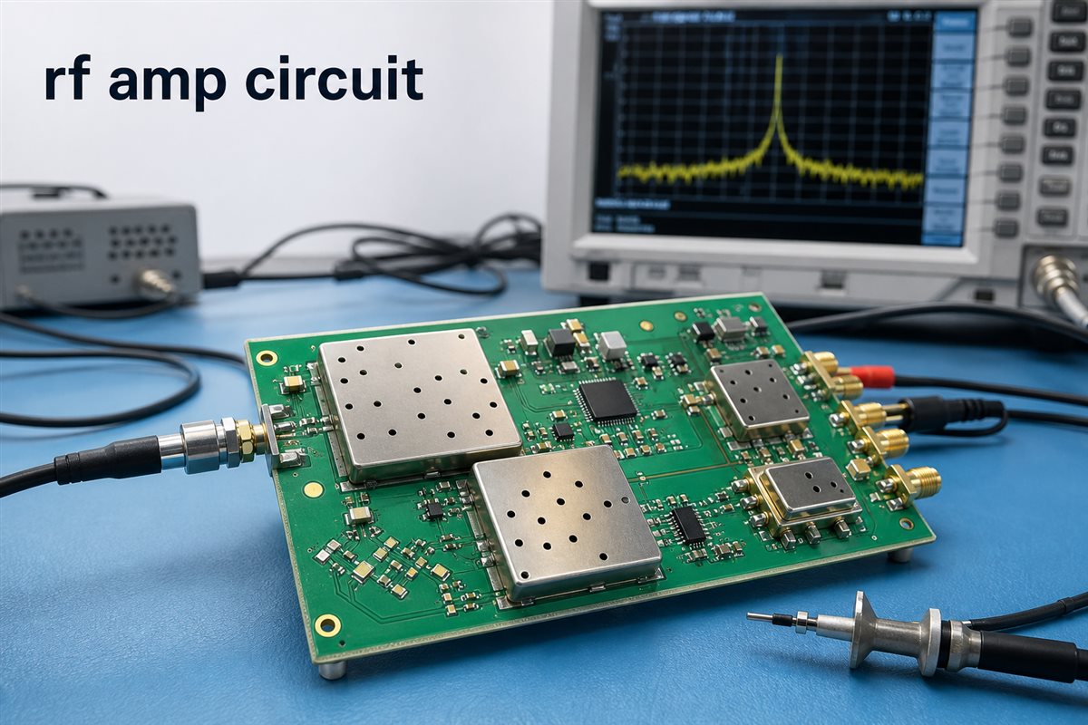
An rf amp circuit is used to increase the strength of a radio frequency signal before it reaches an antenna, receiver stage, RF module, coaxial cable, or test system. For engineers and buyers, the practical question is not only how the circuit works, but whether the RF amplifier board can be manufactured, assembled, inspected, and tested reliably.

That is where PCB and PCBA review becomes important. An RF amp circuit may involve controlled impedance, SMA connectors, RF materials, grounding, shielding, copper thickness, thermal control, component placement, soldering, and RF testing. EBest Circuit (Best Technology) supports RF-related PCB fabrication, component sourcing, SMT assembly, through-hole assembly, inspection, and small-batch PCBA projects. If your RF amplifier project is ready for manufacturing review, please send your Gerber files, stackup, BOM, RF notes, connector drawing, and test requirements to sales@bestpcbs.com.
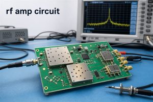
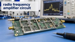
rf amp circuit

What Is an RF Amp Circuit?

An RF amp circuit is a radio frequency amplifier circuit that increases RF signal power, voltage, or current within a specified frequency range.

It may be used in:

  • wireless communication modules
  • RF test equipment
  • antenna systems
  • receiver front ends
  • transmitter output stages
  • IoT and telemetry products
  • industrial RF modules
  • medical or sensing equipment
  • satellite or base station related products

The exact circuit function depends on the customer’s RF design. Some RF amplifiers focus on low noise. Some focus on output power. Some need wide bandwidth. Some need high linearity. Some must work with a 50 ohm RF path and SMA or coaxial connectors.

For PCB manufacturing, the most important point is not to redesign the amplifier. The customer’s RF design team should define the frequency, gain, active components, matching network, and performance target. The PCB manufacturer’s role is to help turn approved circuit files into a stable PCB or PCBA build.

RF Amp Circuit vs RF Amplifier Circuit

In many searches, rf amp circuit and rf amplifier circuit mean almost the same thing. “Amp” is simply a shorter way to say “amplifier.”

However, the wording can reveal different user expectations:

Search TermCommon Search Intent
rf amp circuitShort search for circuit explanation, example, or board project
rf amplifier circuitMore formal circuit explanation
radio frequency amplifier circuitEducational explanation or technical reference
rf power amplifier circuitHigher output power or transmitter-related circuit
rf amplifier moduleProduct/module level search
amplifier circuit PCBPCB manufacturing or assembly angle

For this article, the focus is not only the circuit idea. The focus is what happens when an RF amplifier circuit becomes a manufacturable PCB and PCBA project.

If the board is poorly laid out or poorly assembled, even a correct schematic may perform badly. Problems such as impedance discontinuity, poor grounding, long RF traces, wrong connector footprint, weak solder joints, heat buildup, or shield contact issues can affect the final result.

RF Power Amplifier Circuit vs Low Noise Amplifier Circuit

RF amplifier circuits are not all the same. Two common categories are RF power amplifier circuits and low noise amplifier circuits.

Circuit TypeMain GoalPCB/PCBA Concern
RF power amplifier circuitIncrease output powerHeat, copper, grounding, current path
Low noise amplifier circuitPreserve weak signal qualityNoise, shielding, short RF path
Broadband RF amplifierWork across wide frequency rangeStable impedance and layout symmetry
RF driver amplifierDrive the next RF stageMatching and thermal stability
RF module amplifierIntegrated product functionConnector, enclosure, testing

For a power amplifier, copper thickness, heat spreading, via placement, component derating, and solder joint strength may become important. For a low noise amplifier, the layout is usually more sensitive to grounding, shielding, leakage paths, component placement, and noise coupling.

EBest Circuit does not decide the amplifier topology for the customer. That belongs to the RF design side. Our value is to review whether the PCB files, stackup, material, assembly notes, and test requirements match the manufacturing path.

Radio Frequency Amplifier Circuit Diagram and PCB File Review

A radio frequency amplifier circuit diagram is only one part of the production package. Before a board can move into fabrication and assembly, the manufacturer needs enough files to understand both the electrical and mechanical requirements.

Useful production files include:

  • Gerber or ODB++ files
  • PCB stackup drawing
  • BOM with approved part numbers
  • CPL / pick-and-place file
  • Assembly drawing
  • Schematic or RF notes when allowed
  • Connector datasheets
  • Controlled impedance requirements
  • SMA or coaxial connector drawing
  • Shielding or enclosure notes
  • Testing requirements
  • Packing and labeling requirements

For RF projects, missing information can create real production risk. For example, a connector may appear correct in the BOM but require a specific board thickness, edge clearance, solder pad geometry, or mounting style. A controlled impedance trace may be drawn correctly in layout software but still need stackup confirmation before fabrication.

Before production, EBest Circuit can review the manufacturing files and raise EQ questions if something needs confirmation. This is especially useful when the project includes RF connectors, impedance control, high-frequency material, shielding cans, or mixed SMT and through-hole assembly.

50 Ohm Impedance in RF Amp Circuit PCB Manufacturing

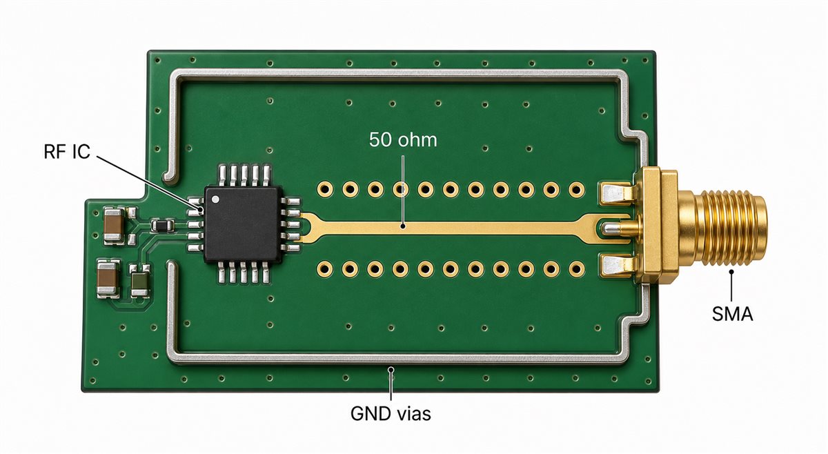
Many RF amp circuit boards use a 50 ohm signal path. This is common for RF test equipment, coaxial cables, SMA connectors, antennas, RF modules, and many communication systems.

A 50 ohm path is affected by trace width, copper thickness, dielectric thickness, material dielectric constant, solder mask condition, reference plane distance, connector transition, via structure, and manufacturing tolerance.

The 50 ohm requirement should be confirmed before fabrication, not only checked after the board is made. If impedance control is required, the stackup, trace width, dielectric thickness, copper thickness, and test coupon should be reviewed together.

For RF PCBs, EBest Circuit can support controlled impedance review and provide impedance test reports when required by the customer. For related RF material and manufacturing options, customers can also review our RF PCB capability page.
rf amp circuit

SMA Connectors, Grounding, and Shielding in RF Amp Circuit Boards

SMA connectors are common in RF amp circuit boards because they provide a practical interface between the PCB and coaxial cable, antenna, RF instrument, or external module.

SMA connector reliability depends on more than the part number.

Key manufacturing details include:

  • PCB thickness at the connector area
  • edge-launch or through-hole connector type
  • center pin pad geometry
  • ground terminal contact
  • solder mask opening
  • mounting hole or flange requirement
  • connector height and mechanical clearance
  • coaxial cable direction
  • soldering method
  • final inspection access

Grounding and shielding are equally important. RF amplifier boards may use ground vias, via fences, shielding cans, connector shell grounding, enclosure contact, or separated RF and power areas. If the board uses a shielding can, the solder pads must allow stable attachment. If the project uses board-level shielding, the PCBA process should keep shield placement, soldering, and inspection clear.

A related EMI shield PCB article may be useful when the RF amplifier board also has shielding structures or enclosure-level EMI control.

RF Amp Circuit PCB Materials and Stackup Choices

The material choice for an RF amp circuit board depends on frequency, loss requirement, board thickness, cost target, thermal need, and the customer’s approved RF design.

Common options may include:

  • standard FR4 for lower-frequency or cost-sensitive RF products
  • high-Tg FR4 for better thermal and process margin
  • Rogers or other RF laminate for lower loss or tighter RF performance
  • hybrid stackup when RF and digital/power sections share one board
  • metal core or thermal structure when heat is a major concern

Not every RF amplifier board needs expensive RF laminate. Some lower-frequency or less sensitive projects can be manufactured with carefully controlled FR4. However, higher-frequency, high-power, low-noise, or insertion-loss-sensitive projects may require better material control.

For manufacturing review, the stackup should match the RF path, power path, grounding strategy, assembly method, and mechanical requirement. A stackup that looks acceptable electrically but is difficult to laminate, drill, plate, or assemble may create production risk.

Thermal Control for RF Power Amplifier Circuit Boards

RF power amplifier circuits can generate heat. If the heat is not controlled, performance and reliability may suffer.

Thermal review may involve:

  • copper thickness
  • large copper areas
  • thermal vias
  • component pad design
  • heat spreading path
  • board thickness
  • solder joint reliability
  • component derating
  • shield or enclosure heat path
  • test condition and operating duty cycle

For higher-power RF boards, the heat path should be discussed before production. The PCB manufacturer can review copper thickness, via process, material selection, solderability, and assembly feasibility, but the customer should define the power level, thermal simulation target, enclosure condition, and operating environment.

If the project is related to a higher-power amplifier, our previous article on high power RF amplifier circuit can be used as a supporting reference.

SMT Assembly and Testing for RF Amp Circuit PCBA

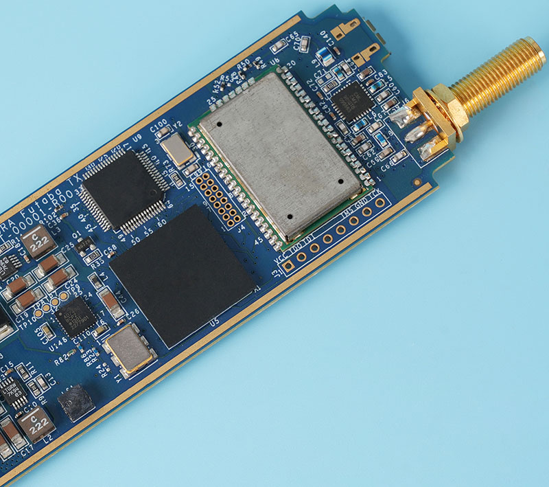
RF amp circuit PCBA projects often include small RF components, SMA connectors, shield cans, regulators, matching components, filters, inductors, capacitors, and sometimes through-hole or mechanical parts.

Small quantity does not mean low process risk.

Assembly risks may include:

  • wrong RF component value
  • component rotation
  • poor solder wetting
  • tombstoning of small passives
  • SMA solder joint weakness
  • shield can solder gap
  • connector tilt
  • flux residue near RF areas
  • thermal pad voiding
  • inspection blind spots

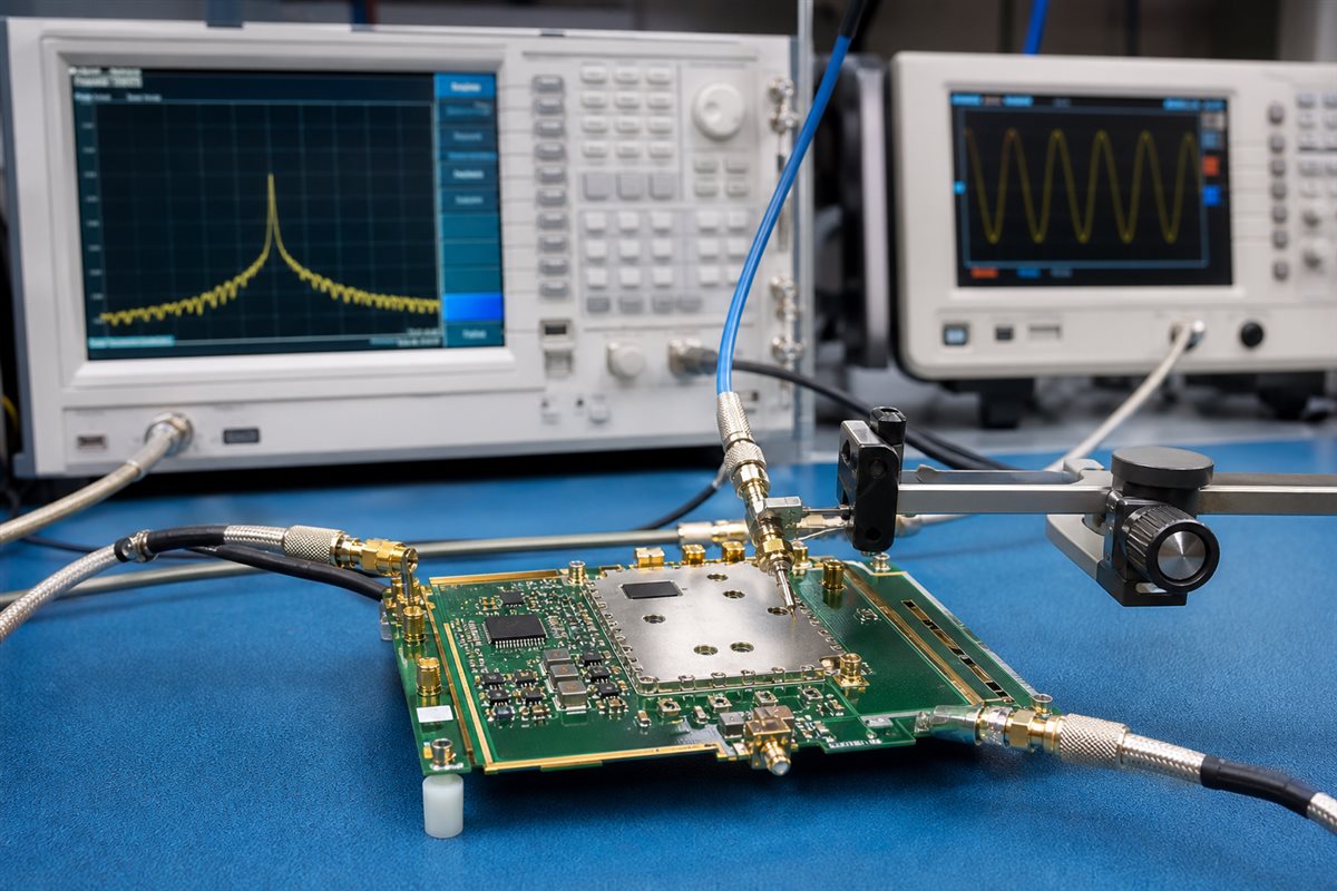
Testing also needs planning. Some projects only need visual inspection and electrical continuity. Others may require RF performance testing, functional testing, programming, or fixture-based verification. When RF test requirements are defined by the customer, EBest Circuit can coordinate the manufacturing and assembly side so the boards are prepared for the required test method.

For PCBA projects, the most useful test notes are practical: test points, connector access, pass/fail criteria, fixture needs, labeling method, and packing requirements.
rf amp circuit

RF Amp Circuit Manufacturing Case Study

A U.S. customer needed a small batch of RF amplifier PCB assemblies for a wireless test module used during engineering validation. The board was not a simple FR4 prototype. It needed stable RF transmission, connector reliability, clean assembly, and test-ready delivery.

Project requirements:

  • Customer region: USA
  • Application: Wireless RF test module
  • Quantity: 20 pcs pilot build
  • PCB type: 4-layer RF amplifier PCB
  • Material: High-Tg FR4 with RF path review
  • Finished thickness: 1.6mm +/-10%
  • Copper thickness: 1oz finished copper
  • Surface finish: ENIG
  • Connector: SMA interface for RF input/output
  • Impedance: 50 ohm RF trace control
  • Assembly: SMT + connector assembly
  • Testing: Visual inspection, electrical test, and customer-defined RF test preparation
  • Delivery target: Prototype-to-pilot build schedule

Manufacturing challenges:

  • The SMA connector footprint and board thickness had to match the connector drawing.
  • The 50 ohm RF trace needed stackup and trace geometry review before fabrication.
  • Ground via placement and shield-related pads had to remain clear for assembly.
  • Small RF passives required correct orientation and stable SMT control.
  • The customer needed boards packed safely for lab validation after assembly.

EBest Circuit solution:

  • Reviewed Gerber, stackup, BOM, CPL, connector drawing, and RF notes together.
  • Confirmed the impedance structure before production.
  • Checked SMA pad geometry, grounding area, solder mask opening, and connector clearance.
  • Prepared PCB fabrication and SMT assembly under one workflow.
  • Inspected connector solder joints, RF component placement, board cleanliness, and packing method.
  • Kept production notes visible from file review to final shipment.

Result:

The customer received 20 RF amplifier PCB assemblies ready for engineering validation. The value was not only making the PCB. The value was keeping RF path, connector mounting, impedance control, SMT assembly, inspection, and packing details connected before the boards reached the customer’s test bench.

This is the type of project where one unclear connector note or one missed impedance requirement can delay the whole validation schedule. A controlled manufacturing review helps reduce that risk before the pilot build starts.

Why Choose EBest Circuit for RF Amp Circuit PCB Projects?

EBest Circuit is suitable for RF amp circuit PCB and PCBA projects when the customer needs more than bare board fabrication.

What EBest Circuit can support:

  • RF PCB fabrication
  • FR4, high-Tg FR4, RF laminate, and hybrid material review
  • Controlled impedance review
  • SMA and RF connector assembly support
  • SMT assembly and through-hole assembly
  • Component sourcing based on approved BOM
  • DFM and assembly file review
  • Electrical testing and inspection
  • Small-batch and pilot production
  • Packing and delivery coordination

EBest Circuit has worked in PCB and PCBA manufacturing since 2006. The company supports prototype, small-batch, and production projects for customers in more than 40 countries and regions. Quality support includes ISO9001, ISO13485, IATF16949, AS9100D, RoHS, REACH, and UL-related documentation.

For RF amp circuit projects, stable engineering communication matters. The board may involve RF traces, connectors, controlled impedance, shielding, thermal concerns, and assembly details at the same time. EBest Circuit’s engineering and production teams can help keep those details visible before fabrication and assembly begin.

FAQs About RF Amp Circuit

1. What is an RF amp circuit?

An RF amp circuit is a radio frequency amplifier circuit used to increase RF signal strength within a defined frequency range. It may be used in wireless modules, antenna systems, RF test equipment, transmitters, receivers, and communication products.

2. Is an RF amp circuit the same as an RF amplifier circuit?

Yes, in most searches they mean the same thing. “RF amp circuit”is a shorter phrase, while “RF amplifier circuit”is the more formal term.

3. Does an RF amp circuit PCB always need 50 ohm impedance?

Not always, but many RF amplifier boards use 50 ohm paths because SMA connectors, coaxial cables, antennas, and RF instruments commonly use 50 ohm systems. The exact requirement should come from the customer’s RF design.

4. Can EBest Circuit design the RF amplifier circuit?

EBest Circuit does not replace the customer’s RF design team. The active device, topology, gain target, matching network, and RF performance target should come from the customer. EBest Circuit can review PCB manufacturability, stackup, impedance, connector mounting, assembly, and testing requirements.

5. What files should I send for RF amp circuit PCB manufacturing?

Useful files include Gerber or ODB++, stackup drawing, BOM, CPL file, assembly drawing, connector datasheets, impedance notes, RF test requirements, and packing instructions.

All in all, an rf amp circuit project is not only about the amplifier schematic. It is about making sure the RF path, PCB material, impedance, connector, grounding, shielding, assembly, inspection, and testing requirements can move through production without avoidable confusion. If your project is ready for PCB or PCBA review, please send your files and questions to sales@bestpcbs.com.
You may also like

Precision RF Power Amplifier Circuit Design & Assembly
Monday, January 5th, 2026

An RF power amplifier circuit is the critical engine that boosts weak radio frequency signals to power levels sufficient for transmission through antennas, forming the backbone of all wireless communication. This comprehensive guide delves into the principles of precision RF power amplifier circuit design and assembly, exploring core concepts from basic topologies to advanced 5G applications, and outlining the PCB manufacturing considerations essential for optimal performance and reliability.

For RF design engineers, developing a high-performance RF power amplifier circuit​ is often a formidable challenge. What are the most common hurdles they face?

  • Achieving Target Efficiency & Linear Output:​ Balancing high power-added efficiency (PAE) with stringent linearity requirements across the desired bandwidth, often leading to iterative, time-consuming design cycles.
  • Ensuring Thermal & Signal Stability:​ Managing heat dissipation from high-power RF transistors and preventing unwanted oscillations or performance drift, which can cause system failure.
  • Navigating Complex PCB Materials & Stack-ups:​ Selecting the right high-frequency laminate (e.g., Rogers, ceramic-filled) and designing a stack-up that minimizes loss and supports effective grounding, often without in-house fabrication expertise.
  • Integrating Precise Biasing & Control Circuits:​ Designing a stable bias circuit for RF power amplifiers​ that ensures consistent quiescent point operation over temperature and aging, critical for both linear and saturated amplifiers.
  • Transitioning from Schematic to Reliable Physical Assembly:​ Accurately translating an RF power amplifier circuit diagram​ into a manufacturable layout while managing impedance, parasitics, and ensuring robust PCB and PCBA​ assembly for field reliability.

The path from a conceptual RF power amplifier circuit design​ to a stable, high-yield product requires a partnership with a fabrication expert. Here is how a specialist provider addresses these core challenges:

  • Co-Design for Performance:​ Leveraging simulation-driven design support to help optimize matching networks and layout for target efficiency, linearity, and bandwidth from the outset.
  • Thermal & EMI-Optimized Platforms:​ Offering advanced materials like ceramic PCBs (AlN, Al₂O₃) and thermally enhanced FR4, alongside design rules for thermal vias and shielding, to ensure stability.
  • Material Science & Engineering Guidance:​ Providing expert consultation on RF-suitable dielectrics (Dk, Df), copper roughness, and stack-up configuration to meet electrical performance goals.
  • Integrated Passive & Bias Solutions:​ Enabling the fabrication of precision embedded resistors and stable DC feed networks as part of the PCB to simplify the RF power amplifier bias circuit.
  • Precision High-Frequency Manufacturing:​ Utilizing controlled impedance routing, advanced plating, and stringent assembly processes (e.g., for MOSFET RF power amplifier circuits) to ensure the built circuit matches the designed performance.

At EBest Circuit (Best Technology), we specialize in turning complex RF designs into reliable RF products. As a professional manufacturer of high-frequency PCBs and ceramic PCB​ substrates, we provide a seamless, one-stop service from engineering support and prototype fabrication to full turnkey assembly. Our expertise ensures your precision RF power amplifier circuit​ is built on a foundation optimized for signal integrity, thermal management, and long-term durability. For your next RF power amplifier circuits project, pls feel free to contact our team at sales@bestpcbs.com.

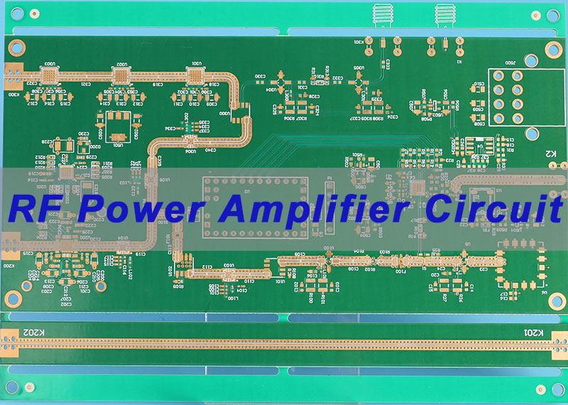
RF Power Amplifier Circuit

What Is RF Power Amplifier Circuit and How Does It Work in RF Systems?

An RF Power Amplifier (PA) circuit is a specialized electronic circuit designed to increase the power level of a radio frequency signal before it is delivered to an antenna for radiation. Its core function is to take a low-power RF input signal, typically from an oscillator or upconverter, and amplify it to a level sufficient for transmission over a required distance, while maintaining signal fidelity as defined by system requirements such as linearity, bandwidth, and efficiency.

The operation of an RF power amplifier in a circuit​ can be distilled into a few key stages and principles:

  • Input Matching Network:​ This block (often an input tank circuit) maximizes power transfer from the signal source (e.g., driver stage) to the active device (transistor) by transforming impedance, reducing reflections.
  • Active Amplification Device:​ The core where power amplification occurs. This can be a BJT​ (for Class C BJT RF power amplifier circuit), a MOSFET​ (for MOSFET RF power amplifier circuit), or GaAs/GaN HEMTs for higher frequencies and powers.
  • Bias Network:​ Provides the proper DC operating point (quiescent current/voltage) to the transistor. The design of this bias circuit for RF power amplifiers​ is crucial for setting the amplifier class (A, AB, B, C) and ensuring stability.
  • Output Matching Network:​ Transforms the high-impedance output of the transistor down to the standard load impedance (e.g., 50Ω). It also filters harmonics and ensures maximum power is delivered to the antenna.
  • Power Supply & Conditioning:​ Delivers stable, clean DC power. For RF power amplifier circuits with AGC, additional control loops are integrated to dynamically adjust gain.

In essence, the RF power amplifier circuit​ acts as the final, powerful “voice” of an RF transmitter, determining the effective range and signal quality of the entire system, from a simple RF power amplifier circuit​ in an FM transmitter to a complex 5G RF power amplifier circuit.

RF Power Amplifier Circuit

What Are the Core Design Principles of RF Power Amplifier Circuit Design?

RF power amplifier circuit design​ is governed by a set of competing requirements that must be carefully balanced. The goal is to meet target specifications for frequency, bandwidth, output power, gain, efficiency, and linearity, all while ensuring stability and manufacturability. Precision in this process separates a functional prototype from a robust, high-yield product.

The core principles revolve around managing trade-offs:

Design PrincipleKey GoalPrimary Trade-Off / Challenge
Impedance MatchingMax Power Transfer, Low VSWRBandwidth vs. Complexity
LinearityLow Distortion (ACLR)Linearity vs. PAE
Efficiency (PAE, η)Minimize DC Waste, Reduce HeatInverses Linearity
Stability (K>1)Unconditional StabilityStability vs. Gain
Gain & BandwidthTarget Gain over Required BWGain-Bandwidth Product
Thermal ManagementJunction Temperature ControlPower Density vs. Cooling

A practical RF power amplifier circuit design 27MHz NPN​ for citizen-band radio will prioritize efficiency (often using Class C) and simplicity. In contrast, a wideband RF power amplifier circuit​ for a vector signal analyzer must maintain flat gain and good linearity over a multi-octave bandwidth, often employing feedback or distributed amplification techniques. Understanding these principles is the first step in any RF power amplifier design tutorial circuit​ and is essential whether aiming for a low power RF amplifier circuit​ or a 100W RF power amplifier mini circuit.

Why Is Bias Circuit for RF Power Amplifiers Critical for Stability and Performance?

The bias circuit for RF power amplifiers​ is far more than a simple DC feed; it is a critical control system that sets the fundamental operating mode of the transistor and profoundly impacts nearly all aspects of performance, reliability, and stability. An imprecise or unstable bias point can lead to degraded efficiency, distorted output, thermal runaway, or even catastrophic device failure.

A well-designed bias network addresses several key requirements:

  • Establishes Amplifier Class:​ It sets the quiescent current (IQ). Zero IQdefines Class B/C, a small IQdefines Class AB, and a large IQdefines Class A. This choice directly dictates the efficiency-linearity trade-off.
  • Ensures Thermal Stability:​ Uses techniques like emitter/source degeneration resistors or proportional-to-absolute-temperature (PTAT) bias generators to prevent thermal runaway, where increasing temperature causes current to increase uncontrollably.
  • Suppresses Low-Frequency Oscillation:​ Includes RF chokes and bypass capacitors to isolate the RF signal from the DC supply, preventing unwanted feedback paths that can cause oscillation at very low frequencies.
  • Maintains Performance Over Temperature & Batch Variation:​ Active bias circuits with feedback can compensate for the negative temperature coefficient of a transistor’s turn-on voltage (VBEor VGS(th)), keeping gain and output power consistent.
  • Enables Control & Protection:​ Can integrate circuits for RF power amplifier protection​ (overcurrent, over-temperature) or facilitate dynamic control like AGC (Automatic Gain Control).

For example, a Class C RF power amplifier circuit​ uses a negative or zero bias to achieve high efficiency (>70%) but is highly nonlinear, suitable only for constant-envelope modulation. Conversely, a RF linear power amplifier circuit​ for 5G requires a precise Class-AB bias to operate in its linear region, making the bias circuit’s stability paramount to maintain low EVM and ACLR. In a MOSFET RF power amplifier circuit, gate bias voltage must be tightly controlled, as a small drift can cause a large shift in drain current and linearity.

How to Read an RF Power Amplifier Circuit Diagram and Understand Its Blocks?

An RF power amplifier circuit diagram​ is the roadmap from which a physical circuit is built. Learning to interpret it is essential for design, troubleshooting, and assembly. While details vary, most diagrams for a discrete RF power amplifier circuit PA​ (Power Amplifier) can be broken down into functional blocks.

A typical block-level breakdown of a circuit diagram of RF power amplifier​ includes:

  • DC Power Input & Decoupling:​ Shows the VCC/VDDconnection and an array of capacitors (bulk, ceramic, RF) to ground. This network provides stable DC and shunts any RF on the supply line to ground.
  • Input Matching Network (IMN):​ A network of inductors (L), capacitors (C), and sometimes transmission lines located between the input connector and the transistor’s base/gate. Its goal is to present the optimal impedance (often the complex conjugate of S11) to the transistor for maximum power transfer at the fundamental frequency.
  • Active Transistor & Bias Network:​ The centerpiece (Q1 or M1). The bias circuit​ is shown connected to the base/gate (and sometimes emitter/source). It may consist of voltage dividers, current mirrors, or active regulator circuits supplying the critical DC bias voltage/current.
  • Output Matching Network (OMN):​ Located between the transistor’s collector/drain and the output connector. It transforms the device’s optimal load impedance (for max. power or efficiency) down to 50Ω and often acts as a low-pass filter to attenuate harmonic frequencies generated by the nonlinear transistor.
  • Load (Antenna) & Isolation:​ The output port, often with a directional coupler or isolator/circulator symbol to denote protection from load mismatches.

Reading a diagram for a VHF RF power amplifier circuit​ versus a UHF RF power amplifier circuit​ will show different component values and layout notations due to the wavelength difference. A simple RF power amplifier circuit​ may combine bias and matching into minimal components, while a high power RF amplifier circuit​ diagram will prominently feature thermal pads, balancing resistors for power combining, and robust supply traces. Understanding these blocks allows you to analyze any design, from a FM transmitter circuit with RF power amplifier stage​ to a sophisticated RF power amplifier integrated circuit​ evaluation board schematic.

What Is the Difference Between Simple RF Power Amplifier Circuit and High Power RF Amplifier Circuit?

The distinction between a simple RF power amplifier circuit​ and a high power RF amplifier circuit​ extends far beyond the output power rating. It represents a fundamental shift in design complexity, component selection, and required supporting infrastructure to manage the challenges of high power density.

The differences are multifaceted:

AspectSimple / Low Power RF PAHigh Power RF PA
Primary GoalGain, Functionality, CostEfficiency, Linearity, Reliability
Active DeviceSmall-signal BJT/MOSFET (SMD)Power LDMOS/GaN/GaAs (Flange/Ceramic)
Bias CircuitSimple resistive dividerActive, compensated bias
Matching NetworkLumped L/C, simpleHybrid lumped/distributed, harmonic tuning
Thermal Mgmt.Passive (PCB/heatsink)Active cooling, Ceramic PCB/Metal-clad
Power SupplyStandard regulatorHigh-current, low-noise, sequenced
StabilityBasic isolationFull protection circuits, isolators
ArchitectureSingle-endedPower-combined, Push-Pull

A 5W RF power amplifier circuit​ for a handheld radio exemplifies a mid-range design, needing careful layout but not extreme cooling. A 100W RF power amplifier mini circuit​ is an engineering feat, pushing the limits of power density. The RF power amplifier circuit design​ for such high-power applications is inseparable from the PCB and PCBA​ strategy, mandating materials with high thermal conductivity (like alumina ceramic) and sophisticated assembly processes to handle the immense thermal and electrical stresses.

How Does a Class C RF Power Amplifier Circuit Operate in RF Applications?

A Class C RF power amplifier circuit​ is designed for maximum possible efficiency by biasing the active transistor significantly below its cutoff point. The transistor conducts current for less than half​ of the input RF cycle, producing a highly distorted, pulsed output current that is rich in harmonics. A tuned output tank circuit​ (resonant at the fundamental frequency) filters out these harmonics, reconstructing a sinusoidal waveform at the output.

Key Operational Characteristics:

  • Bias Point:​ The base/gate is biased negatively (for BJTs) or below threshold (for MOSFETs), ensuring the device is off​ with no input signal.
  • Conduction Angle:​ Typically 120° to 180°, but often much less. Efficiency (η) is theoretically given by: η = (θ – sinθ) / (4(sin(θ/2) – (θ/2)cos(θ/2)))**​ where θ is the conduction angle. Lower angle = higher efficiency (>70% possible).
  • High Nonlinearity:​ The amplified output is not a linear reproduction of the input. This makes Class C unsuitable for amplitude-based modulations (AM, QAM).

Common RF Applications:

  • Constant-Envelope Transmitters:​ Ideal for FM transmitter circuits​ and FM transmitter circuit with RF power amplifier stage, where information is in frequency/phase shifts, not amplitude.
  • RF Heating & Plasma Generation:​ Where pure CW or pulsed RF power is needed, as in industrial Transculpt RF power amplifier circuit schematics 1MHz.
  • Some AM Transmitters:​ Can be used in AM RF power amplifier circuit​ designs with high-level plate/collector AM modulation, though less common today.
  • RFRFPA designing a input tank circuit AMFONE:​ In vintage or hobbyist tube-based designs, Class C is frequently employed for its efficiency.

While a Class-C RF power amplifier circuit​ offers superb efficiency, its use in modern spectrum-conscious, high-data-rate systems is limited. It cannot be used for modern digital modulations like OFDM (used in 4G/5G) which have high peak-to-average power ratios (PAPR) and require linear amplification. Therefore, while foundational in RF amplifier circuit​ history and still valuable for specific apps, it has largely been supplanted by linearized Class-AB or Doherty architectures in mainstream communications.

Where Are 5G RF Power Amplifier Circuit and Wideband RF Power Amplifier Circuit Used Today?

Modern wireless systems demand amplifiers that are not only powerful and efficient but also capable of handling wide bandwidths and complex signals. The 5G RF power amplifier circuit​ and the wideband RF power amplifier circuit​ are two specialized answers to these demands, finding critical roles in next-generation infrastructure and test equipment.

5G RF Power Amplifier Circuit Applications:

  • Massive MIMO Active Antenna Units (AAUs):​ Each antenna element in a 5G base station array is driven by its own PA module. These PAs must be highly linear to support high-order QAM (256QAM, 1024QAM) and wide bandwidths (up to 400MHz in n79 band), all while maintaining excellent efficiency to reduce power consumption and heat.
  • 5G User Equipment (Smartphones, CPEs):​ RF power amplifier integrated circuits​ (PAMiDs) in phones must cover a vast range of 5G sub-6 GHz and mmWave bands, requiring multi-band, multi-mode operation with advanced envelope tracking (ET) for battery life.
  • Small Cells & Repeaters:​ Deployed for network densification, these use PAs with lower output power but stringent linearity and efficiency requirements.

Wideband RF Power Amplifier Circuit Applications:

  • Electronic Warfare (EW) & SIGINT Systems:​ Jamming and surveillance platforms require amplifiers that can operate across very wide instantaneous bandwidths (multiple octaves) to cover diverse threat frequencies.
  • Test & Measurement Equipment:​ Vector signal generators, network analyzers, and wideband signal analyzers use linear wideband PAs in their signal paths to provide flat gain and high output power across their entire frequency range (e.g., 9 kHz to 6 GHz or more).
  • Multi-Standard and SDR Base Stations:​ Software-defined radios benefit from wideband PAs that can be reconfigured for different services (2G/3G/4G/5G, WiFi) without hardware changes.
  • CATV/Broadband Distribution:​ Coaxial cable networks use wideband PAs to amplify dozens of TV and data channels simultaneously.

The design of these circuits pushes the limits of semiconductor technology (using GaN-on-SiC for high power and bandwidth) and RF power amplifier circuit design, often employing techniques like feedback, distributed amplification (traveling-wave), or balanced structures to achieve the necessary performance across a broad spectrum, from a VHF​ to UHF RF power amplifier circuit​ range and beyond.

What PCB and PCBA Factors Affect the Reliability of an RF Power Amplifier Circuit?

The reliability of an RF power amplifier circuit​ is not determined solely by its schematic design; it is equally dependent on the physical implementation—the PCB and PCBA. For a precision, high-power RF design, the substrate material, layout, fabrication quality, and assembly process are non-negotiable elements of performance.

Critical PCB/PCBA Factors for RFPA Reliability:

  • Dielectric Material (Laminate):​ Standard FR-4 has high loss tangent (Df) at RF frequencies, causing signal loss and heat generation. Reliable RF PAs​ use low-loss laminates (Rogers, Taconic) or ceramic PCBs​ (Al₂O₃, AlN) for superior thermal conductivity and stable dielectric constant (Dk).
  • Controlled Impedance & Layout:​ Microstrip traces must be precisely calculated and fabricated to maintain 50Ω impedance. Poor control leads to mismatches, reflected power, gain ripple, and potential instability. Grounding via fences and a solid ground plane are essential.
  • Thermal Design:​ The PCB itself is a heatsink. Use of thermal vias under power device pads, thick copper planes (2oz+), and direct bonding to metal cores or ceramic substrates are vital to transfer heat from the transistor junction. This is the single biggest factor in high power RF amplifier circuit​ longevity.
  • Component Selection & Placement:​ RF components (capacitors, inductors) must have high self-resonant frequencies (SRF) and appropriate power ratings. Placement must minimize parasitic inductance in high-current paths (like the drain/collector supply). Decoupling capacitors must be placed for optimal high-frequency performance.
  • Assembly Process Quality:​ Solder joint integrity is critical. Voids under a power transistor’s thermal pad can cause catastrophic overheating. Precise solder paste application and reflow profiling are mandatory. For MOSFET RF power amplifier circuits, ESD protection during handling is crucial.

A failure in any of these areas can lead to degraded output power, increased noise, intermittent operation, or thermal runaway. Partnering with a PCB/PCBA​ provider like Best Technology, which understands these RF power amplifier circuits’ unique needs—from material selection to precision RF power amplifier circuit​ assembly—is fundamental to transitioning a great design into a reliable, field-deployable product.

RF Power Amplifier Circuit

To sum up, RF power amplifier circuits​ are the indispensable force multipliers in the wireless world, determining the reach, clarity, and efficiency of every transmitted signal. This guide has explored their core principles, from interpreting a basic RF power amplifier circuit diagram​ to the advanced demands of 5G​ and wideband​ designs, and underscored the critical role of precision PCB and PCBA​ in achieving reliable performance.

Success in precision RF power amplifier circuit design & assembly​ requires a synergy of expert electrical design and masterful physical implementation. This is where EBest Circuit (Best Technology)​ provides decisive value. We combine engineering support for high-frequency design with advanced manufacturing capabilities for low-loss RF laminates and high-thermal-conductivity ceramic PCBs. Our controlled impedance fabrication and rigorous assembly processes ensure your design performs as intended, from prototype through volume production. Ready to amplify your next RF project with precision? Pls feel free to contact our engineering sales team anytime at sales@bestpcbs.com.

You may also like