





A radio frequency amplifier circuit is used when an RF signal needs to be amplified for wireless communication, antenna systems, RF modules, signal repeaters, test equipment, industrial sensors, or high-frequency control boards. For engineers, the circuit may start from a schematic, but the final result depends heavily on PCB material, stackup, impedance, grounding, component placement, RF connector transition, SMT assembly, and testing conditions.
EBest Circuit (Best Technology) supports RF-related RF PCB fabrication, stackup review, controlled impedance production, component sourcing, SMT assembly, inspection, and small-batch PCBA manufacturing. If your RF amplifier project has Gerber files, stackup notes, BOM, impedance requirements, connector drawings, or assembly files, please send them to sales@bestpcbs.com for engineering review before production.
What Is a Radio Frequency Amplifier Circuit?
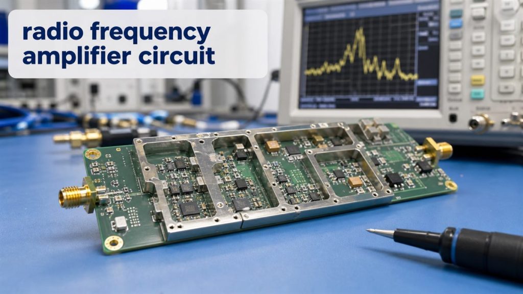
A radio frequency amplifier circuit increases the strength of a high-frequency signal. It may be used near an antenna, inside a wireless module, in a signal repeater, or on a test board where RF signals need stable gain.
The PCB is not only a carrier for the circuit. At RF frequencies, the board becomes part of the signal path. Copper traces, dielectric material, ground return, vias, solder mask, pads, and connectors can all affect signal behavior.
Common applications include:
- wireless communication modules
- antenna front-end circuits
- RF test boards
- signal repeaters
- IoT gateways
- industrial RF sensors
- high-frequency control boards
- measurement equipment
For sourcing, the useful question is not only whether a supplier can make the PCB. The better question is whether the supplier can keep RF material, impedance, connector, SMT, and testing details visible before production starts.
Radio Frequency Amplifier Circuit Diagram and PCB File Review
A radio frequency amplifier circuit diagram helps explain the RF input, amplifier device, matching network, bias circuit, power filtering, ground reference, and RF output. But for production, the diagram is only one part of the project.
EBest Circuit needs the manufacturing files that define the real board:
| File | Why It Matters |
| Gerber / ODB++ | Copper, solder mask, outline, RF pads |
| Stackup | Material, dielectric thickness, copper thickness |
| BOM | RF component value, package, sourcing |
| CPL | Placement position and orientation |
| Connector drawing | Footprint, board edge, mounting method |
| Impedance notes | 50 ohm or other impedance control needs |
| Assembly drawing | Soldering, shielding, cleaning, packing notes |
EBest Circuit does not replace the customer’s RF design team. The amplifier topology, frequency band, gain target, noise figure, matching network, and RF performance decision should come from the customer’s engineering side. Our role is to check whether the PCB and PCBA files can be built reliably according to those requirements.
RF Amplifier Circuit Board Materials and Stackup
RF amplifier circuit board material selection depends on frequency, loss requirement, thermal need, cost, and product environment.
For some lower-frequency or cost-sensitive RF projects, FR4 may be acceptable. For higher-frequency or lower-loss RF applications, high-frequency laminate or hybrid material may be needed. EBest Circuit supports normal Tg FR4, mid Tg FR4, high TG PCB materials, Isola 370HR, FR408HR, Rogers 4003, Rogers 4350, Rogers 5880, Taconic material, PTFE material, and hybrid material options when required.
For RF boards, material choice affects dielectric constant, dielectric loss, impedance calculation, insertion loss, and stability. This is why stackup should be confirmed before fabrication, especially when the board includes SMA connectors, 50 ohm RF traces, shielding areas, or impedance reports.
A practical material review should answer:
- What frequency range will the board support?
- Is FR4 acceptable, or is a high-frequency material required?
- Does the Dk/Df value affect the RF performance target?
- Does the board need high Tg material for thermal reliability?
- Is this a pure RF board or a hybrid RF + digital board?
- Does the surface finish match solderability and RF requirements?
For RF boards above hundreds of MHz, material and process selection should be handled more carefully. For higher-frequency applications, dielectric loss, copper roughness, drilling, plating, and surface treatment become more sensitive.
50 Ohm Impedance in RF Amplifier PCB Manufacturing
Many RF amplifier PCB projects use 50 ohm single-ended impedance. The value is usually defined by the customer’s RF engineer, but the PCB manufacturer must build the physical structure consistently.
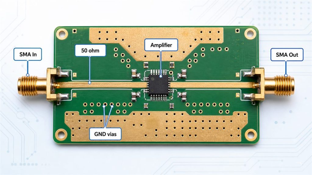
A 50 ohm trace is not decided by trace width alone. It depends on trace width, copper thickness, dielectric thickness, dielectric constant, reference ground layer, solder mask coverage, finished etching result, connector transition, and via/ground structure.
EBest Circuit’s PCB capability data shows that standard 1oz outer-layer line/space can reach 4/4mil in normal process and 3/3mil in special process. For RF amplifier PCB manufacturing, this matters because the finished trace is what the signal actually sees. If the design uses SMA connectors, the transition from connector pad to RF trace also needs attention. Ground pads, via fences, solder mask openings, and edge clearance should follow the customer-approved RF layout.
If an impedance report is required, the impedance coupon and testing requirement should be planned before production, not added after the board is finished.
Low Noise Amplifier Circuit PCB Manufacturing Checks
A low noise amplifier circuit is usually placed near the receiver side. The signal is weak, so the board should avoid adding unnecessary instability before the RF design can do its job.
For LNA boards, the manufacturing review is not about changing the RF design. It is about protecting the approved design during fabrication and assembly.
- Do not change the RF input path without approval.
- Keep the approved ground structure visible in production files.
- Confirm RF component package and part number before sourcing.
- Check small passive component footprints before SMT.
- Review solder mask opening around RF pads.
- Protect connector and RF input areas during handling.
- Keep cleaning requirements clear when flux residue may matter.
A common risk is component substitution. In RF circuits, a capacitor, inductor, resistor, or filter may look like a standard component in the BOM, but its value, tolerance, package, ESR, Q factor, or approved manufacturer may matter. If sourcing changes are needed, they should be confirmed with the customer before SMT.
RF Power Amplifier Circuit Heat and Copper Requirements
An RF power amplifier circuit may generate more heat than a small-signal amplifier. The PCB must support both RF signal quality and thermal reliability.
EBest Circuit’s PCB capability data supports conventional FR4 inner copper from HOZ to 5oz and outer copper from 1oz to 5oz, with heavier copper available as a special process. This gives engineers more manufacturing options when an RF power board needs stronger current capacity or heat spreading.
Copper is not only about current. It can affect heat spreading, trace geometry, etching compensation, impedance calculation, solder mask bridge feasibility, board balance, warpage risk, and soldering quality.
If a power amplifier device has an exposed pad, large thermal pad, or heat-sensitive area, SMT process review is also important. Solder paste opening, void control, thermal vias, copper balance, and reflow profile can affect the final assembly.
For some high-power or heat-sensitive products, the project may also need metal core PCB, ceramic PCB, high-Tg FR4, or special thermal structure review. The right choice depends on power level, operating temperature, mechanical design, and customer test requirements.
SMT Assembly Risks for Radio Frequency Amplifier Circuit Boards
RF amplifier boards often include small passive components, RF filters, amplifier ICs, inductors, capacitors, shielding parts, SMA connectors, and sometimes QFN or BGA assembly requirements. The assembly risk is not only “can the component be placed?” The real question is whether the board can be soldered, inspected, cleaned, tested, and packed without damaging RF performance or connector reliability.
A practical SMT workflow may include:
incoming PCB and component review -> baking when required -> solder paste printing -> SPI -> placement -> reflow -> post-reflow inspection -> AOI -> X-Ray when BGA is involved -> hand soldering -> cleaning -> testing -> labeling -> depaneling -> packing
This process matters because many RF board problems appear before final testing. SPI can catch solder paste issues such as insufficient paste, offset, bridging risk, and paste height variation. SPI inspection accuracy around 10um is useful for fine components and RF matching areas.
- RF passive value and package
- connector orientation
- solder paste volume near small components
- soldering around SMA or RF terminals
- flux residue near RF paths
- shield can soldering
- QFN/BGA inspection when used
- packing protection for protruding connectors
Small quantity does not remove process risk. One failed prototype can delay debugging, RF validation, customer approval, and the next production build.
Testing and Inspection for RF Amplifier PCB Assembly
RF amplifier PCB assembly needs two different types of checks.
Manufacturing inspection: checks whether the board was made and assembled according to the production files.
RF performance testing: checks whether the circuit meets the customer’s electrical target.
For manufacturing-side control, EBest Circuit can support bare PCB electrical testing, impedance testing when required, AOI after SMT, X-Ray for BGA or hidden solder joints when needed, visual inspection of SMA connectors and RF terminals, solder joint and cleanliness inspection, and packing inspection before shipment.
For RF performance testing, the customer should define the test frequency, input signal condition, output condition, gain target, power level, load condition, acceptable tolerance, pass/fail criteria, and required test fixture or cable setup.
This distinction helps avoid confusion. A PCB supplier can verify manufacturing quality and coordinate customer-defined testing, but RF gain, noise figure, frequency response, and final electrical acceptance should be based on the customer’s approved test method.
Radio Frequency Amplifier Circuit Manufacturing Case Study
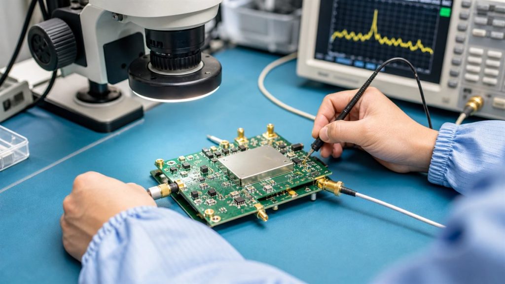
A USA customer needed a small-batch RF amplifier PCB assembly for a wireless signal test module. The order quantity was not large, but the project had RF connector requirements, 50 ohm signal routing, small RF components, and assembly cleanliness requirements.
| Item | Requirement |
| Customer region | USA |
| Application | Wireless RF signal test module |
| Quantity | 30 pcs prototype and pilot build |
| PCB type | 4-layer RF-related FR4 PCB |
| Material | High-Tg FR4 |
| Finished thickness | 1.6mm +/-10% |
| Copper | 1oz outer copper, 0.5oz inner copper |
| Surface finish | ENIG |
| RF requirement | 50 ohm signal path |
| Assembly | SMT plus RF connector assembly |
| Packing | Single-unit protection after inspection |
Main project risks:
- The RF connector had to be soldered firmly and protected during packing.
- The 50 ohm path had to match the customer-approved layout.
- Small RF passives needed correct package, value, and approved sourcing.
- RF areas needed clean soldering and inspection.
- The first build had to support validation before the next production stage.
EBest Circuit solution:
- Reviewed Gerber, stackup, BOM, CPL, connector drawing, and assembly notes together.
- Checked RF trace area, connector footprint, ground vias, and solder mask opening.
- Confirmed component packages and sourcing risks before SMT.
- Used ENIG for stable solderability and surface protection.
- Checked connector soldering, board cleanliness, and packing method before shipment.
- Coordinated inspection and testing according to the customer’s project notes.
Result: The customer received a controlled RF amplifier PCBA pilot build for validation. The value was not only producing 30 boards. The value was keeping RF connector mounting, impedance-related PCB manufacturing, BOM preparation, SMT assembly, inspection, and packing requirements connected under one workflow.
FAQs About Radio Frequency Amplifier Circuit
1. What is a radio frequency amplifier circuit used for?
It is used to amplify RF signals in wireless communication, antenna systems, RF modules, signal repeaters, sensors, test equipment, and industrial electronics.
2. Does a radio frequency amplifier circuit always need a 50 ohm PCB trace?
Not always, but many RF amplifier PCB projects use 50 ohm impedance. The exact requirement should come from the customer’s RF design and product specification.
3. Can FR4 be used for an RF amplifier circuit board?
FR4 can be used for some lower-frequency or cost-sensitive RF projects. Higher-frequency, lower-loss, or more stable RF applications may require Rogers, PTFE, or other high-frequency materials.
4. What files should I send for RF amplifier PCB manufacturing?
Useful files include Gerber or ODB++, drill files, stackup, BOM, CPL, assembly drawing, impedance notes, connector drawing, and test requirements.
5. Can EBest Circuit design the RF amplifier circuit?
EBest Circuit supports PCB fabrication, DFM review, component sourcing, SMT assembly, inspection, and testing coordination. The RF circuit design, frequency target, gain requirement, and matching network should be confirmed by the customer’s RF engineering team.
All in all, a radio frequency amplifier circuit project should not be treated as only a schematic or only a bare PCB order. RF signal path, material, stackup, impedance, components, SMT assembly, connector reliability, inspection, and testing notes need to stay connected before production starts. If you are preparing an RF amplifier PCB or PCBA project, please send your Gerber files, stackup, BOM, connector drawing, impedance notes, and assembly requirements to sales@bestpcbs.com.
You may also like

Tags: radio frequency amplifier circuit, RF Amplifier PCB, rf pcb assembly