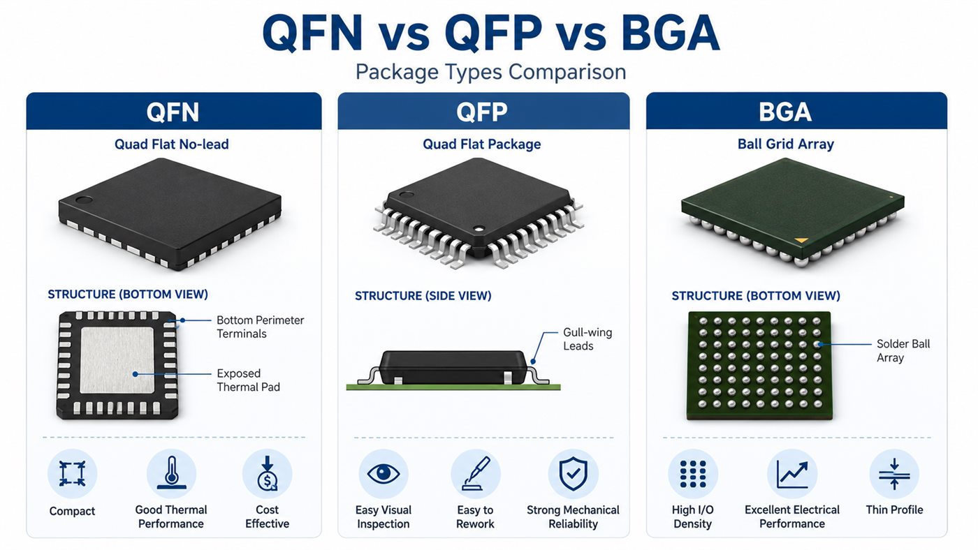
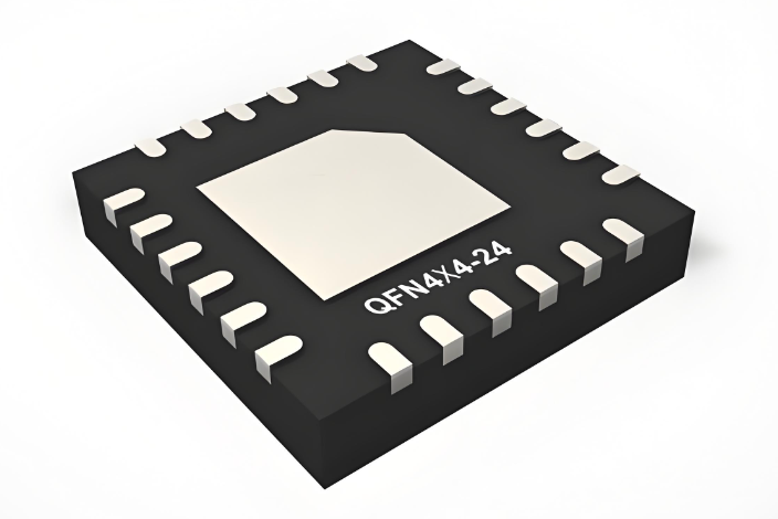
A quad flat no leads package, usually called QFN, is a surface-mount IC package with flat metal terminals along the four edges of its underside. Unlike a QFP, it has no projecting gull-wing leads. Many QFNs also expose a central metal pad that transfers heat into the PCB and may provide an electrical connection. The short connections save space, but most solder joints sit beneath the component. Reliable assembly therefore starts with the exact package drawing—not simply a label such as “QFN-16”—and a matching copper, solder-mask and stencil design.
This article follows the connection from silicon die to PCB, showing how the package structure affects layout and assembly. At EBest Circuit, we support PCB fabrication, component sourcing and PCB assembly. For a QFN-based design, we can review the fabrication and assembly files with your component requirements before production.
Key Takeaways
- No-lead does not mean no terminals: QFN contacts are flat rather than projecting beyond the body.
- Wire-bonded and flip-chip QFNs use different internal connections; both can connect to the PCB through bottom terminals.
- The TI TPS62130 provides a concrete example: a 16-terminal, nominal 3 × 3 mm VQFN with 0.5 mm pitch.
- The exposed pad has a device-specific electrical function. Its net connection must come from the datasheet.
- Package dimensions, PCB copper lands and stencil apertures describe three different geometries.
- Segmented paste openings control solder volume. Paste coverage is not the same measurement as post-reflow voiding.
- Wettable flanks improve optical access to perimeter fillets; hidden center-pad solder still needs an appropriate inspection plan.
What Is a Quad Flat No Leads Package?
A quad flat no leads package is a low-profile IC housing whose four-sided bottom terminals solder directly to PCB lands. “Quad” refers to the four terminal-bearing sides; “no leads” describes the absence of long external leads.
The name does not identify the circuit inside. A QFN may contain a voltage regulator, interface IC, sensor or controller. Nor does “no-lead” certify lead-free chemistry: package construction and material compliance are separate specifications.
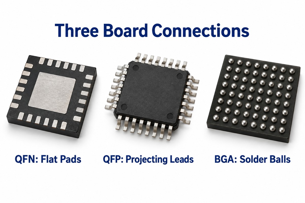
| Package | Board connection | Contact arrangement |
| QFN | Flat solderable terminals | Four underside edges |
| DFN / SON | Flat solderable terminals | Two opposite underside edges |
| QFP | Projecting gull-wing leads | Four sides outside the body |
| BGA | Solder balls | Array beneath the body |
How Do Signals Travel Through a QFN Package?
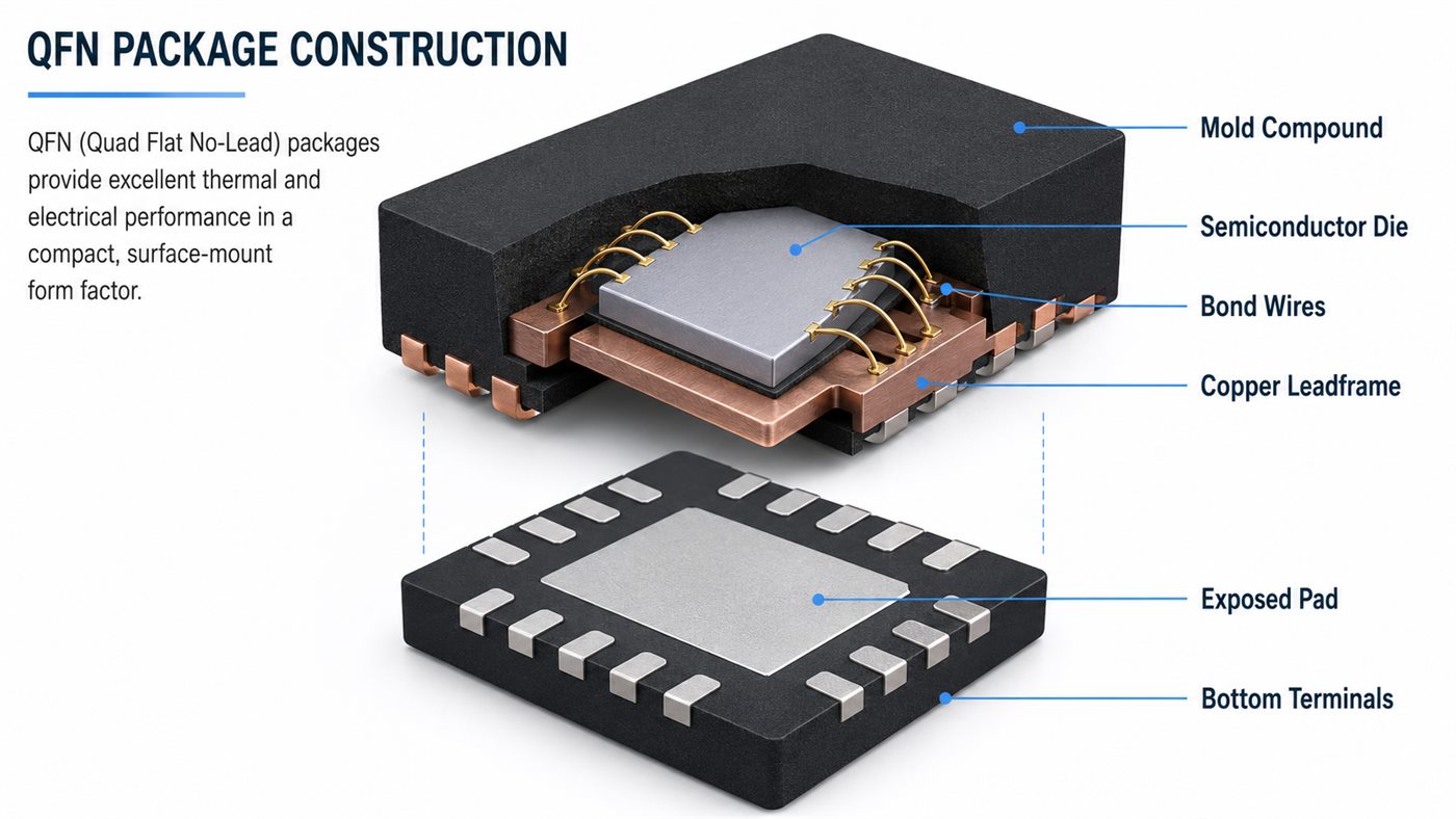
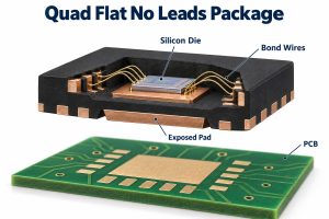
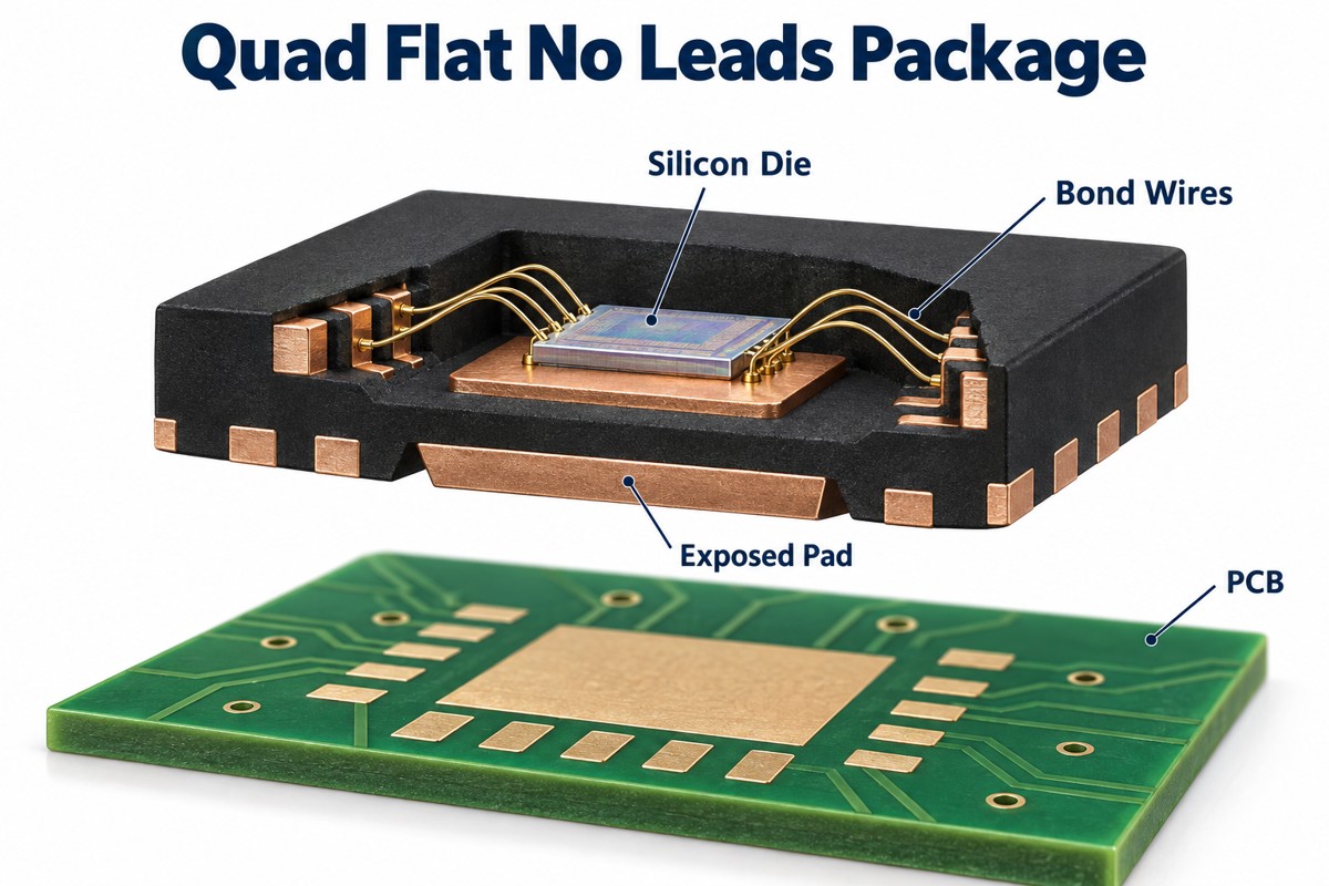
In a conventional wire-bonded QFN, signals travel from the silicon die through bond wires, leadframe terminals and solder joints to PCB copper.
The die sits on a metal paddle inside the molded body. Fine wires connect its bond pads to separate terminal fingers around that paddle. After assembly, solder joins each bottom terminal to its corresponding PCB land. The signal path and the main downward heat path therefore use different parts of the package.
A flip-chip QFN replaces the internal bond-wire connection with bumps or copper pillars. That does not make its external board connection a BGA. The component can still have flat underside terminals. Check the manufacturer’s construction description when internal inductance, current paths or thermal behavior affect the circuit.
QFN Package Process Flow
A typical wire-bonded QFN package process flow includes die attachment, wire bonding, molding, package separation and testing. This semiconductor packaging process takes place before PCB assembly.
- Attach the die: secure the silicon to the leadframe’s die pad.
- Make internal connections: bond wires from die pads to terminal fingers.
- Mold the body: protect the die and wires while retaining the designed external contact surfaces.
- Separate the packages: use the specified saw or punch process.
- Inspect and test: check finished components before packing for board assembly.
Plating, marking and test order vary by package process. At EBest Circuit, our relevant service is mounting the finished IC onto your PCB, not fabricating the semiconductor die or its molded QFN package. This distinction matters when preparing an RFQ: we need the complete component part number and board assembly files.
QFN Package Dimensions: A 3 × 3 mm Example
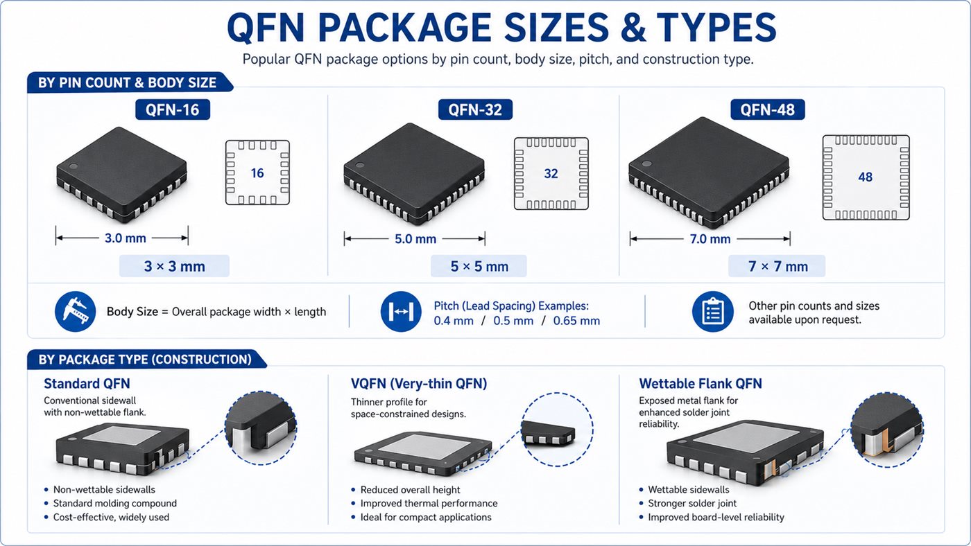
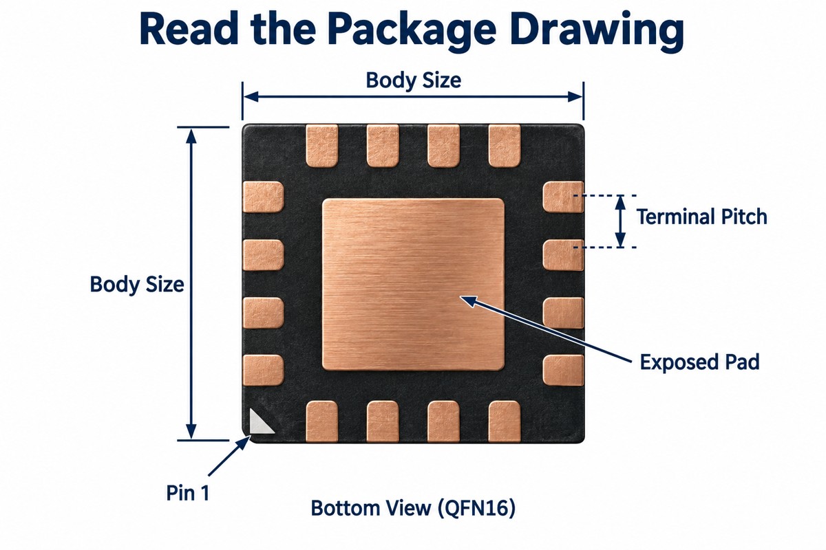
The TI TPS62130 uses a nominal 3 × 3 mm, 16-terminal VQFN with 0.5 mm pitch. Its RGT package drawing shows why the terminal count alone cannot define a footprint.
| Drawing item | RGT0016C example |
| Body length and width | 2.9–3.1 mm each |
| Terminal count | 16 perimeter terminals |
| Terminal pitch | 0.5 mm |
| Maximum package height | 1.0 mm |
| Exposed-pad dimension | 1.68 ± 0.07 mm square |
These are package dimensions from the cited drawing, not universal QFN dimensions or ready-made PCB pad sizes. For a production release, match the complete orderable part number to its current drawing revision. A QFN package datasheet may provide separate package-outline, land-pattern and paste-layout pages; each serves a different purpose.
What Does the Exposed Pad Do?
The exposed pad provides a short heat path from the die into the board and may also carry a required electrical connection.
For the TPS62130 example, the thermal pad connects to ground as directed by its datasheet. Do not transfer that connection to another IC by assumption. A different device may assign its exposed pad a different potential or give specific isolation instructions.
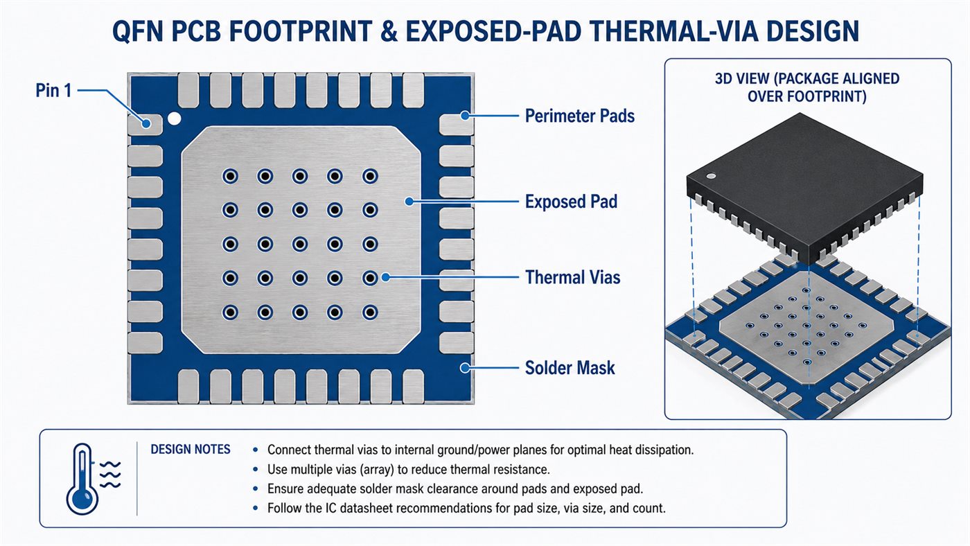
The complete heat path includes the die attachment, package paddle, solder joint, PCB copper and surrounding environment. Thermal vias can connect the top land to internal or opposite-side copper, but their treatment affects soldering. An open hole within the paste area can drain solder during reflow. Via location, plugging or filling must therefore be agreed with the PCB fabricator and assembler rather than added as an isolated layout detail.
How Does the Package Drawing Become a PCB Footprint?
The package drawing defines the component; the recommended land pattern translates that geometry into PCB copper and solder-mask openings.
Start with the exact manufacturer’s land pattern, then review fabrication tolerances and assembly access. Copying the body outline into a footprint does not establish a solderable connection.
- Terminal lands: match the pin numbering and pitch, then check pad length and width against the recommended pattern.
- Center land: use the specified electrical net and review its separation from perimeter pads.
- Solder mask: check clearance and whether the intended mask webs can be manufactured.
- Thermal vias: define hole position and treatment in the fabrication notes.
- Placement data: verify pin 1, centroid rotation and the assembly drawing together.
Our broader QFN package guide covers additional package families and size-selection questions. For the board release itself, keep the component drawing, copper land and paste aperture data as separate checks.
How Should Solder Paste Be Divided Under a QFN?
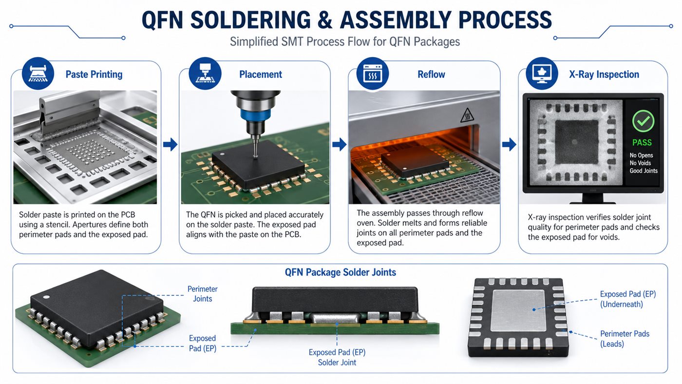
Use separate peripheral apertures and segmented openings over the exposed pad, with the total paste volume matched to the component’s assembly guidance.
TI’s QFN and SON PCB Attachment guide gives approximately 50–70% exposed-pad paste coverage as a typical design approach. This is a starting point from that guide, not a universal acceptance limit. A full-size central opening can deposit too much paste and lift the body, leaving insufficient contact at the outer terminals.
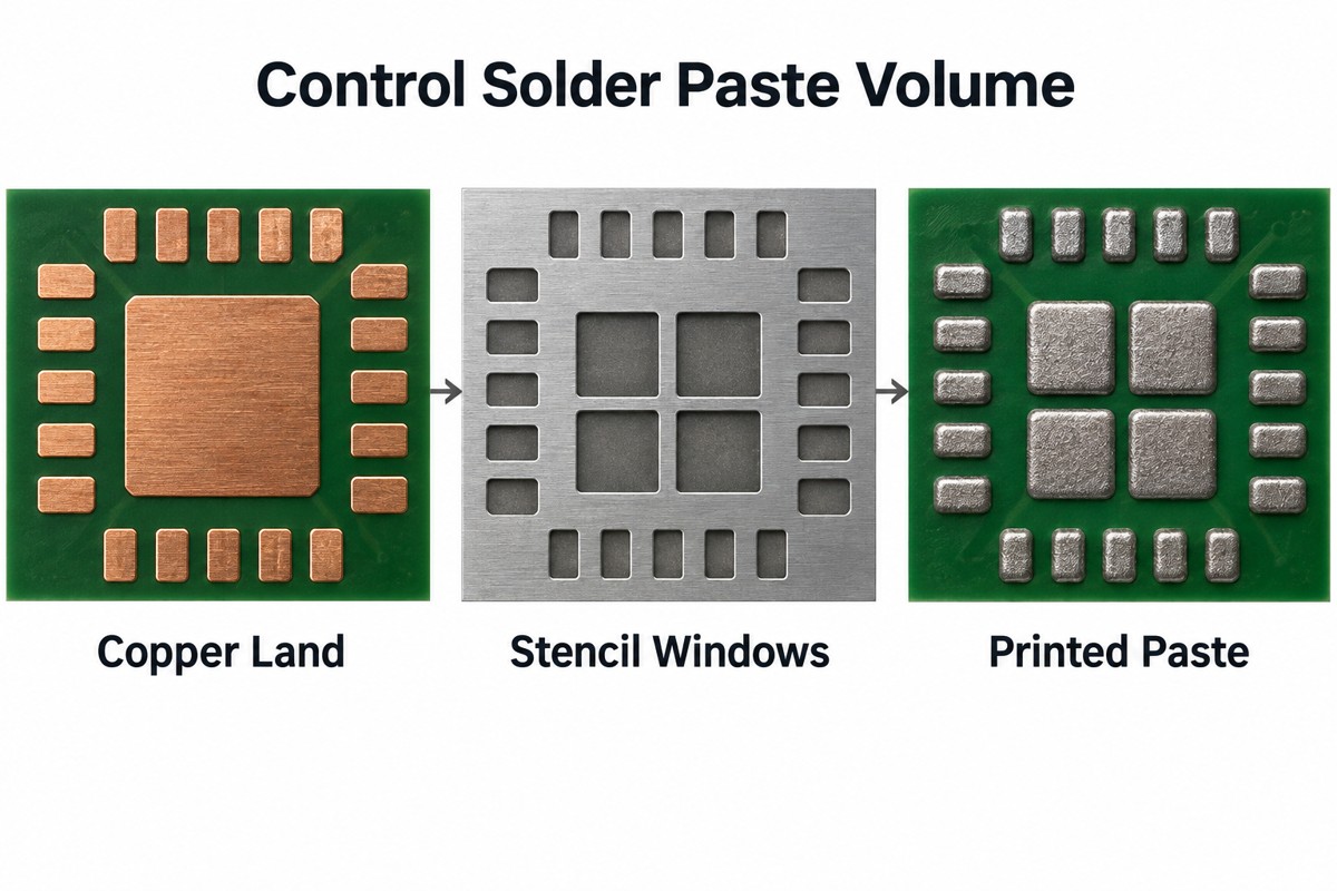
Coverage describes the printed opening area relative to the center land. Voiding describes gaps in the solder joint after reflow. They are not interchangeable percentages. Stencil thickness also changes deposited volume, so identical coverage can produce different results with different foils.
Our SMT stencil service supports the printing stage of PCB assembly. For QFN package soldering, review the paste layer alongside the board design, then check actual deposits with SPI before placement. The reflow profile must suit the solder paste while respecting the component’s temperature and moisture-handling limits.
What Changes When a QFN Has Wettable Flanks?
Wettable flanks provide solderable side features that make perimeter fillets easier to inspect optically.
A conventional sawn terminal may expose bare copper at its side. That surface does not always form a visible fillet, even when the bottom connection is soldered. Pull-back terminals sit inward from the body edge and do not offer the same side-view access.
Wettable-flank versions use features such as plated steps or dimples to support visible solder formation. Confirm the feature in the exact package specification and use its matching land pattern. Side fillets help AOI evaluate the perimeter, but they do not show the entire soldered center pad beneath the body.
How Are Hidden QFN Joints Checked?
X-ray inspection examines hidden QFN solder features, while electrical or functional testing checks circuit behavior. Neither replaces control of the paste-printing process.
| Method | Primary check |
| SPI before placement | Paste volume, height, area and position |
| AOI after reflow | Orientation, placement and accessible solder features |
| X-ray after reflow | Hidden solder distribution, bridges and void patterns |
| Electrical / functional test | Specified connections and operating behavior |
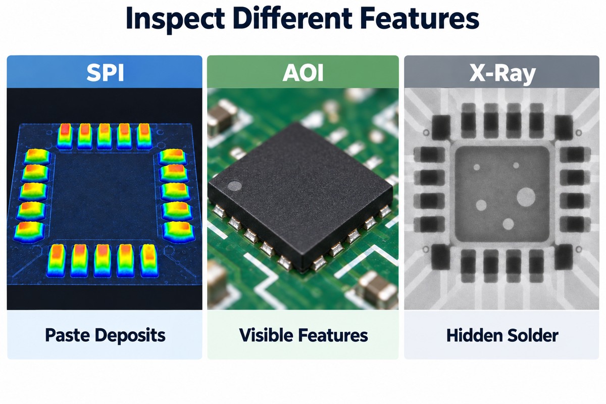
A void limit must come from the applicable component guidance and agreed product requirements. Total void area alone cannot describe every thermal or reliability concern. Location, distribution and the heat-flow path also matter. A normal-looking 2D projection cannot prove every interface has wetted correctly.
At EBest Circuit, we have 3D SPI, AOI and X-ray inspection resources for PCBA work. We establish the inspection and test scope for the actual assembly rather than treating one passing image as evidence that every requirement has been met.
FAQ About Quad Flat No Leads Packages
Does QFN mean the package contains no lead metal?
No. “No-lead” refers to external connection geometry. Lead-free status concerns materials and must be checked in the manufacturer’s environmental declaration or orderable-part information.
Can I solder a QFN using only a soldering iron?
An iron may reach some perimeter contacts, but it usually cannot form the hidden center-pad joint properly. A controlled reflow or rework process is more suitable when the underside pad must be soldered.
Can a QFN be replaced after assembly?
Yes, with a qualified rework process. Heat all solder joints sufficiently before lifting the package, clean and inspect the lands, then control paste deposition and alignment for replacement. Pulling before the joints melt can damage PCB pads.
Does a 260°C package rating mean I should set every reflow zone to 260°C?
No. A package-body temperature limit is not an oven-zone recipe. Use the paste supplier’s profile guidance and measure the assembled board’s actual temperature history without exceeding component limits.
Can conformal coating correct a weak QFN solder joint?
No. Coating protects against specified environmental exposure; it cannot replace a missing electrical connection or restore the intended thermal solder path. Inspect and resolve assembly defects before coating.
How Can EBest Circuit Support Your QFN PCB Assembly?
We can support the board-level work around your selected QFN: PCB fabrication, component sourcing, stencil preparation, SMT assembly and the agreed inspection and testing.
Send your Gerber or ODB++ files, BOM with full manufacturer part numbers, pick-and-place data and quantities to sales@bestpcbs.com. Include any exposed-pad, thermal-via or inspection requirements. We can review those details with you and prepare a quotation for the actual build.