PCB manufacturing PCB manufacturing
Home > Blog

PCB Teardrops in PCB Design: Pads, Vias and Layout Rules

June 24th, 2026

PCB teardrops are small copper reinforcements added where a trace connects to a pad, via, plated hole, or track junction. They reduce weak copper necks, improve drill tolerance, and help PCB fabrication stay more stable when the layout uses small pads, narrow traces, dense routing, or tight annular rings.

In real manufacturing, slight drill shift, etching variation, layer registration tolerance, and thermal stress can affect copper continuity. PCB teardrops give critical transition points more copper support without changing the circuit function. When used correctly, they improve DFM quality, reduce avoidable production defects, and support more reliable PCB assembly.

PCB Teardrops, https://www.bestpcbs.com/blog/2026/06/pcb-teardrops/

What Are PCB Teardrops in PCB Design?

PCB teardrops are tapered copper extensions placed between a PCB trace and a pad, via, plated through hole, or track junction. The copper gradually widens from the narrow trace into the larger copper feature, creating a stronger and smoother transition.

The working principle is simple: a teardrop in PCB design increases the copper area at the weakest connection point. If drilling is slightly off-center or etching removes a small amount of copper, the reinforced area still has more margin than a plain narrow neck.

PCB teardrops are a DFM improvement, not a repair method for poor layout rules. Correct pad size, annular ring, drill tolerance, trace width, spacing, and solder mask clearance must still be designed properly before teardrops are added.

What Does a Teardrop Look Like on a PCB?

A teardrop PCB feature usually looks like a small drop-shaped, oval, rounded, or tapered copper area where a trace enters a pad or via. It is wider near the pad and narrower near the trace, so the copper transition does not look abrupt.

On a via, it may look like a smooth copper neck flowing into a round via pad. On an SMD pad, it may look like a short copper wedge connected to the pad edge. On a track junction, it may appear as a rounded fillet that softens the width change.

A good teardrop should be clean, centered, and controlled. It should not touch another net, create copper slivers, break clearance rules, or interfere with solder mask openings. The final shape must be checked in the real copper output, not only in the layout view.

PCB Teardrops, https://www.bestpcbs.com/blog/2026/06/pcb-teardrops/

What Types of Teardrops Are Commonly Used in PCB Layout?

Common teardrops in PCB layout include curved arc teardrops and straight linear teardrops. The right type depends on board density, signal speed, reliability level, available spacing, and manufacturing tolerance.

  • Curved Arc Teardrops
    Curved arc teardrops use a rounded copper transition from the trace to the pad, via, or track junction. The smooth edge helps distribute mechanical stress more evenly and provides better geometry continuity. This type is recommended for high-frequency PCB, high-reliability PCB, automotive electronics, medical PCB, aerospace PCB, and Class 3 reliability designs.
  • Straight Linear Teardrops
    Straight linear teardrops use a diamond-like or linear copper transition. They occupy less routing space and are easier to fit into compact PCB layouts. This type is suitable for ordinary low-speed PCB, dense HDI routing, 0201 components, fine-pitch QFN pads, and tight fanout areas.

For high-reliability or high-speed PCB design, curved arc teardrops are usually preferred. For compact low-speed layouts where spacing is limited, straight linear teardrops can be a more practical choice.

Why Use Teardrops on PCB Pads, Vias and Tracks?

Teardrops are used because pads, vias, and track junctions are common weak points in PCB copper geometry. A narrow trace entering a larger pad may lose copper margin if drilling, imaging, or etching has normal production variation.

  • Pads: Teardrops reinforce SMD pads, through-hole pads, connector pads, and component lands. This helps reduce trace neck damage near solder joints and improves reliability under thermal cycling or mechanical force.
  • Vias: Teardrops reduce drill breakout risk around small via pads and tight annular rings. They are useful in dense routing, HDI PCB, BGA fanout, and multilayer PCB designs where registration tolerance is limited.
  • Tracks: Teardrops smooth trace width changes, T-junctions, and neck-down areas. This reduces sharp copper stress points and helps avoid open circuits caused by weak copper transitions.

For customers, the practical value is fewer open circuits, lower rework risk, more stable prototype validation, and better batch production yield.

How Do PCB Teardrops Improve PCB Manufacturing Quality?

PCB teardrops improve manufacturing quality by adding copper margin at points affected by drilling, imaging, plating, etching, and layer registration tolerances. These tolerances are normal in PCB fabrication, especially on dense multilayer boards and small via designs.

During drilling, the hole may not land exactly in the center of the pad. During etching, a narrow trace may lose a small amount of copper width. If the trace-to-pad neck is already weak, the remaining copper can become too thin or even open. PCB teardrops reduce this risk by widening the transition area.

They also support better process stability when the board has small annular rings, fine traces, fine-pitch pads, and compact via fanout. In batch production, this can reduce scrap, lower inspection pressure, and improve long-term reliability.

For PCBA projects, teardrops also help protect copper near pads that experience soldering heat, connector insertion force, vibration, or repeated thermal cycling. They do not replace good fabrication control, but they add useful manufacturing tolerance.

When Should PCB Teardrops Be Used?

PCB teardrops should be used when the layout has limited copper margin, small pads, narrow traces, tight drilling tolerance, or high reliability requirements. They are most valuable when a normal manufacturing shift could weaken a copper connection.

Use teardrops in these cases:

  • Small vias with tight annular rings or limited pad diameter.
  • Fine traces connected to larger pads, vias, or plated holes.
  • Through-hole connectors exposed to plug-in force or vibration.
  • Flex and rigid-flex PCB near bend exits or rigid-to-flex transitions.
  • High-vibration electronics used in automotive, industrial, robotics, or outdoor equipment.
  • Dense multilayer PCB where layer registration tolerance is tighter.
  • Prototype designs moving into stable batch production.

If pads are large, traces are wide, spacing is generous, and reliability demand is low, teardrops may not bring obvious manufacturing value. In that case, clean routing and standard DFM rules are more important.

Where Are Teardrops Commonly Used in PCB Layout?

Teardrops are commonly used at trace exits, via connections, plated hole pads, connector pads, fine-pitch component pads, and narrow track junctions. These areas often carry higher manufacturing, assembly, or mechanical risk.

Typical locations include:

  • Via fanout areas near ICs, BGAs, and dense routing channels.
  • Connector pads where repeated insertion may stress solder joints.
  • Through-hole pads for terminals, headers, switches, and power pins.
  • Fine-pitch SMD pads where trace width is much smaller than pad width.
  • Flex PCB pad exits where copper fatigue may happen.
  • Track neck-down areas where trace width changes sharply.
  • High-current transition areas where copper continuity matters.
  • Test pads and programming pads that may face repeated probing.

The best location is not every pad or every via. It is the area where added copper improves reliability without creating clearance, solderability, impedance, or inspection problems.

What PCB Teardrop Size Rules and Design Specifications Should Be Followed?

PCB teardrop size rules should follow PCB manufacturer capability, copper spacing, annular ring, solder mask clearance, drill tolerance, and signal requirements. There is no single universal size for every teardrop PCB design.

A practical rule is to make the teardrop large enough to reinforce the copper neck, but small enough to avoid spacing and mask issues. Small vias and large vias should not use the same setting. HDI routing usually needs smaller, cleaner teardrops because clearance is more limited.

For SMD pads, the teardrop should not disturb solder mask openings or solder paste behavior. For high-speed nets, the shape should not create a large sudden copper widening. For rigid-flex PCB, rounded shapes are usually safer than sharp transitions.

ItemTypical RangeCheckpoint
Via length25%–50% pad diameterDrill margin
Via width50%–80% pad diameterAnnular support
SMD length75%–150% trace widthPad transition
SMD width150%–250% trace widthMask spacing
Track length100%–300% trace widthCopper neck
ClearanceSupplier DFM ruleNet safety
ShapeRounded or straightLayout density

Before production, confirm PCB teardrop size rules with the PCB manufacturer, especially for HDI PCB, impedance-controlled PCB, RF PCB, rigid-flex PCB, and fine-pitch assembly. If a teardrop causes spacing violations, solder mask conflict, or impedance concern, reduce the size or remove it from that area.

How Do Teardrops Affect High-Speed PCB Design?

Teardrops can affect high-speed PCB design because they add local copper area and slightly change trace-to-pad geometry. In many standard digital or low-speed circuits, the effect is small. In controlled impedance, RF, and high-speed differential routing, it should be reviewed carefully.

Use extra care in these areas:

  • Controlled impedance traces where copper widening may change local impedance.
  • Differential pairs where both sides should keep similar shape, width, and length.
  • RF launch areas where pad geometry is part of the tuned transition.
  • High-speed via fanout where return path, anti-pad, and via stub all matter.
  • BGA escape routing where clearance and symmetry are limited.
  • Clock, DDR, PCIe, USB, Ethernet, and antenna paths where geometry consistency matters.

High-speed designs can still use teardrops, but they should be selective and symmetrical. Avoid large automatic teardrops on RF launch pads, impedance-controlled neck-downs, or matched differential pairs unless the final geometry has been reviewed.

How to Add Teardrops in KiCad?

KiCad teardrops should be added after the main routing is complete and before final manufacturing output. This avoids repeated changes when traces, vias, pads, or copper zones are still being adjusted.

Step 1: Finish the main PCB routing.
Complete trace routing first, including via placement, pad connections, copper pours, differential pairs, and key spacing rules. Do not add teardrops too early, because later routing changes may distort the teardrop shape or create clearance issues.

Step 2: Check basic design rules.
Run DRC before adding teardrops. Fix trace width, via size, pad clearance, annular ring, and net spacing problems first. PCB teardrops should reinforce a correct layout, not cover existing rule violations.

Step 3: Set teardrop parameters.
Open the teardrop settings and define the shape, length, width, and target objects. For round vias and through-hole pads, use moderate teardrops to improve drill tolerance. For rectangular SMD pads, keep the shape smaller to avoid solder mask or pad spacing problems.

Step 4: Apply teardrops to selected areas.
Apply teardrops to vias, pads, or track junctions based on real need. Small vias, narrow traces, fine-pitch pads, flex PCB exits, and connector pads should be prioritized. Avoid applying large teardrops automatically across high-speed or RF areas.
Step 5: Refill copper zones and run DRC again.
After adding teardrops, refill all copper zones and run DRC again. Check whether any teardrop creates clearance errors, copper slivers, solder mask conflicts, or unwanted copper connections.

Step 6: Review final output files.
Inspect the final Gerber, ODB++, or IPC-2581 files before sending them to the PCB manufacturer. Make sure the PCB teardrops are visible on the correct copper layers and do not affect impedance-sensitive nets, fine-pitch pads, or assembly areas.

Add Teardrops in KiCad, https://www.bestpcbs.com/blog/2026/06/pcb-teardrops/

How to Use Teardrops in Altium Designer?

Altium Designer teardrops should also be used near the final stage of PCB layout, after routing, rule setup, and major copper changes are stable. This keeps the teardrop geometry clean and easier to verify before PCB fabrication.

Step 1: Complete routing and confirm design rules.
Finish all critical routing first, including differential pairs, impedance traces, vias, polygon pours, and connector fanout. Then confirm trace width, clearance, via size, solder mask, and manufacturing rules.

Step 2: Open the teardrop tool.
Use the teardrop command in the PCB editor to add, modify, or remove teardrops. Select whether the teardrops should apply to pads, vias, tracks, or T-junctions. For dense boards, it is better to apply them by selected object type or selected area.

Step 3: Choose the teardrop style.
Use curved arc teardrops for high-reliability, high-frequency, automotive, medical, aerospace, and Class 3 PCB designs. Use straight linear teardrops for ordinary low-speed boards, compact HDI layouts, 0201 components, and fine-pitch QFN areas where spacing is limited.

Step 4: Control size and clearance.
Set the length and width according to pad size, trace width, and available spacing. Do not make teardrops too large. Oversized copper may reduce clearance, affect solder mask openings, or change local impedance around high-speed nets.

Step 5: Apply teardrops and inspect sensitive areas.
After applying teardrops, manually check fine-pitch SMD pads, via fanout areas, differential pairs, RF traces, connector pads, and polygon connections. Remove or reduce any teardrop that creates spacing risk or unwanted copper geometry.

Step 6: Run DRC and review manufacturing data.
Run DRC after teardrops are added. Then review the final copper output to confirm that all teardrops are clean, connected to the correct nets, and suitable for PCB manufacturing. For batch production, ask the PCB supplier to include teardrop geometry in the DFM review.

What Mistakes Should Be Avoided When Using PCB Teardrops?

The biggest mistake is adding PCB teardrops automatically without reviewing the final copper geometry. Teardrops should improve manufacturability, not create new production or signal risks.

Avoid these mistakes:

  • Using oversized teardrops that violate copper clearance or create solder mask conflict.
  • Adding teardrops to every object without considering real manufacturing need.
  • Ignoring fine-pitch SMD pads where extra copper may affect solderability.
  • Creating asymmetry on differential pairs, RF paths, and matched routes.
  • Using teardrops to hide poor annular ring design instead of fixing pad and drill rules.
  • Forgetting to refill polygon pours after teardrop generation.
  • Skipping Gerber or ODB++ output review before fabrication release.
  • Allowing duplicate teardrops from both CAD layout and CAM engineering.
  • Ignoring supplier DFM feedback when teardrops create clearance or plating risk.

A good teardrop should be clean, useful, and manufacturable. If it makes inspection harder, reduces spacing, changes a tuned high-speed transition, or conflicts with assembly requirements, it should be reduced or removed.

 PCB Teardrops, https://www.bestpcbs.com/blog/2026/06/pcb-teardrops/

FAQs About PCB Teardrops

Q1: Can teardrops reduce open-circuit failures in PCB fabrication?
A1: Yes. PCB teardrops can reduce open-circuit risk by adding extra copper at weak trace-to-pad and trace-to-via junctions. This is useful when the trace is narrow or the annular ring is tight. For boards with fine lines below 4 mil, small vias, or dense fanout, teardrops can provide more tolerance against etching loss and drill shift.

Q2: Do teardrops help if the drill hole is slightly off-center?
A2: Yes, but only within reasonable manufacturing tolerance. A teardrop gives the via or plated hole more copper support near the trace connection, so minor drill offset is less likely to break the copper neck. However, it cannot fix a poorly designed annular ring. The pad and drill design should still meet the supplier’s standard tolerance, such as ±3 mil or project-specific capability.

Q3: Are teardrops suitable for HDI PCB routing?
A3: Teardrops can be useful in HDI PCB routing, but the size must be controlled carefully. HDI designs often use microvias, fine traces, and compact BGA fanout, so large teardrops may violate spacing rules. For HDI boards, smaller curved or linear teardrops are usually safer. Clearance, solder mask, via pad size, and final CAM output should be reviewed before production.

Q4: Can teardrops be used on blind vias and buried vias?
A4: Yes. Teardrops can be used on blind vias and buried vias when the CAD tool and PCB manufacturer support the design. They are helpful when the via pad is small or the trace connection is narrow. For HDI stackups, the teardrop geometry should match the via structure, lamination process, and layer registration tolerance. Always confirm with the factory before batch production.

Q5: Will teardrops affect solder paste printing?
A5: They may affect solder paste printing if the teardrop extends too close to the exposed SMD pad area. This is more critical for 0201 components, fine-pitch QFN, BGA pads, and connector pads. The copper shape should not change the paste opening or create solder bridging risk. Solder mask and stencil design should be checked together with the teardrop layout.

Q6: Should teardrops be added to test points?
A6: Teardrops can be added to test points when the pad is small, the trace is narrow, or the point may experience repeated probe contact. They can improve copper strength around the pad edge. For ICT or functional test pads, keep enough spacing around the pad and avoid shapes that may affect probe contact accuracy, especially when test pads are below 1.0 mm.

Q7: Are teardrops useful for connector reliability?
A7: Yes. Connector pads often face insertion force, vibration, cable movement, and thermal cycling. Teardrops can strengthen the copper transition between the trace and the connector pad. This is useful for headers, terminals, board-to-board connectors, and wire harness connectors. For high-stress connectors, teardrops should be combined with proper pad size, mechanical support, and solder joint design.

Q8: Can teardrops help rigid-flex PCB durability?
A8: Yes. Rigid-flex PCB designs often benefit from smooth copper transitions near pad exits and rigid-to-flex transition areas. Rounded teardrops can reduce stress concentration and improve copper fatigue resistance. For dynamic bending applications, avoid vias, sharp corners, and abrupt copper width changes in the bend area. Bend radius, copper grain direction, and coverlay opening should also be reviewed.

Q9: Do teardrops improve current carrying capacity?
A9: Not significantly. Teardrops add copper at a local transition, but they do not replace proper current-carrying design. Current capacity mainly depends on copper thickness, trace width, temperature rise, layer structure, and thermal dissipation. For high-current PCB designs, teardrops may help strengthen transitions, but wider traces, copper pours, thermal vias, and heavier copper are more important.

Q10: Can teardrops be removed after they are generated?
A10: Yes. Most PCB design tools allow teardrops to be modified or removed. They should be removed if they create clearance violations, solder mask conflicts, copper slivers, impedance concerns, or unwanted asymmetry on matched signals. Before fabrication, the final Gerber, ODB++, or IPC-2581 data should be reviewed to confirm that all remaining teardrops are clean and manufacturable.

Q11: Are teardrops better than increasing pad size?
A11: They solve different problems. Increasing pad size improves annular ring and drill tolerance, while teardrops reinforce the trace connection area. If space allows, correct pad sizing is usually the first solution. Teardrops are most helpful when the pad size is limited by dense routing, fine-pitch components, or HDI layout constraints. They should support good design, not replace it.

Q12: What should be confirmed with the PCB manufacturer before using teardrops?
A12: Confirm the manufacturer’s copper spacing, drill tolerance, annular ring capability, solder mask clearance, minimum trace width, and CAM modification policy. For critical projects, also confirm whether the factory will add or adjust teardrops during CAM engineering. For batch orders, request a DFM review before production, especially for HDI PCB, RF PCB, rigid-flex PCB, and Class 3 PCB.

Q13: Do teardrops matter more in prototype or mass production?
A13: They matter in both stages, but the value is different. In prototype builds, teardrops help reduce avoidable fabrication risk and support faster design validation. In mass production, they help stabilize yield and reduce repeated defects. For products moving from prototype to batch production, teardrops should be reviewed together with DFM, assembly process, and inspection criteria.

Q14: Can automatic teardrop generation create hidden problems?
A14: Yes. Automatic generation may create oversized shapes, spacing conflicts, copper slivers, or asymmetry on high-speed nets. This is why DRC and CAM review are necessary after adding teardrops. Automatic tools are useful, but final judgment should consider board density, solder mask, impedance control, via type, and assembly requirements. Critical areas should always be checked manually.

Q15: What is the best file format for teardrop review?
A15: Gerber files are widely accepted, but ODB++ and IPC-2581 are often better for intelligent manufacturing review because they include structured layer and net information. For a complete review, send copper layers, drill files, solder mask, paste layers, stackup, fabrication notes, and netlist. This helps the manufacturer verify teardrop geometry before fabrication and PCBA assembly.

Conclusion

PCB teardrops help improve copper reliability at pads, vias, and track junctions. They are especially useful for fine traces, small vias, HDI PCB, rigid-flex PCB, connector areas, and high-reliability products.

Use teardrops selectively, not blindly. Before production, review annular ring, drill tolerance, solder mask clearance, impedance control, Gerber output, and assembly requirements together. EBest Circuit provides custom PCB fabrication, PCB layout review, DFM checking, PCBA assembly, and global supply. Send your Gerber, ODB++, stackup, BOM, and assembly files for review and quotation: sales@bestpcbs.com.

You may also like

PCB Thermal Relief Design Guidelines for High-Current Circuits

June 24th, 2026

PCB thermal relief is useful for soldering, but in high-current circuits it must be designed carefully. A thermal relief structure uses copper spokes to connect a pad, via, or plated hole to a copper plane. This improves solderability, yet it also reduces the copper cross-section available for current flow.

In low-current areas, this trade-off is usually acceptable. In power input terminals, motor control circuits, LED power boards, automotive PCB assemblies, and heavy copper PCB designs, the same structure may create heat rise, voltage drop, or weak current paths. High-current PCB thermal relief design should balance soldering quality with electrical and thermal reliability.

PCB Thermal Relief, https://www.bestpcbs.com/blog/2026/06/pcb-thermal-relief/

What Is PCB Thermal Relief in High-Current Circuit Design?

PCB thermal relief in high-current circuit design is a controlled copper connection between a power pad, via, or plated hole and a large copper area. Instead of using a full solid connection, the pad connects to the plane through several copper spokes.

These spokes are also called thermal spokes, spoke connections, or relief connections. They reduce heat loss during soldering, helping the pad reach soldering temperature more easily. This is useful when a large copper plane would otherwise pull heat away too fast.

However, high-current circuits are different from ordinary signal circuits. The copper spokes must carry real load current. If the spokes are too narrow, too few, or too long, they may become a current bottleneck, causing heat rise, higher resistance, or reduced long-term reliability.

How Does PCB Thermal Relief Affect Current Flow and Heat Transfer?

PCB thermal relief affects current flow by reducing the effective copper area between the pad and the copper plane. Current must pass through the spokes instead of spreading through a full copper connection.

At the same time, the structure also limits heat transfer. This is helpful during soldering because the pad does not lose heat too quickly. But after the product starts working, the same limited copper path may reduce heat dissipation from power pins, terminals, and hot components.

This is the main design conflict. A narrow thermal relief connection improves solderability, but it may increase current density. A solid copper connection improves current flow and heat spreading, but it may make soldering harder. For high-current PCB, the connection style should be selected by current level, copper thickness, pad size, operating temperature, and soldering process.

Thermal Relief vs Solid Connect: Which Is Better for High-Current PCB?

For high-current PCB, solid connect is usually safer when current capacity and heat dissipation are the priority. Thermal relief is only suitable when solderability is difficult and the spokes are wide enough to carry the required current.

ItemThermal ReliefSolid ConnectBetter Choice
Current capacityLimited by spoke width, spoke count, and copper thicknessHigher because the pad connects fully to copperSolid connect
Heat dissipationLower, because spokes restrict heat flowBetter heat spreading into copper planeSolid connect
SolderabilityEasier to solder, especially on large copper planesHarder to solder due to fast heat lossThermal relief
Voltage dropHigher risk if spokes are narrowLower resistance pathSolid connect
Temperature riseMay increase around spokes under loadLower local heating in most power pathsSolid connect
Mechanical strengthWeaker if spokes are thin or longStronger copper support around padSolid connect
Through-hole power pinsUseful if solder fill is difficult, but spokes must be enlargedBetter for sustained currentCase by case
Power terminalsRisky with default narrow spokesMore reliable for high load and cable stressSolid connect
ConnectorsSuitable for low-current or ground pinsBetter for high-current power pinsMixed rules
Thermal viasUsually not recommendedBetter for heat transferSolid connect
Heavy copper PCBRequires wider custom spokesOften preferred for current pathsSolid connect
ReworkEasier pad heatingMore difficult due to copper heat sinkingThermal relief
Best useModerate current with soldering riskHigh current, heat spreading, low resistanceDepends on priority

A practical choice is simple: use solid connect for sustained high current, thermal pads, bus bars, and heat-spreading areas. Use thermal relief only when soldering risk is higher than current risk. For connectors, mixed rules are often best: signal or ground pins may use relief, while power pins use solid copper or enlarged spokes.

Thermal Relief vs Solid Connect, https://www.bestpcbs.com/blog/2026/06/pcb-thermal-relief/

PCB Thermal Relief Spokes: Width, Number, and Copper Thickness Rules

PCB thermal relief spokes are the most important factor in high-current relief design. Spoke width, spoke count, copper thickness, and spoke length all affect current capacity and heat rise.

Key design rules include:

  • Use wider spokes for high-current nets.
    Narrow spokes create higher resistance and higher current density. Power nets, battery terminals, motor outputs, and high-load connectors should not use small default spokes.
  • Increase spoke count when space allows.
    Four spokes usually provide better current distribution than two spokes. For high-current pads, more copper paths can reduce the load on each spoke.
  • Match spoke width with copper thickness.
    A spoke setting that works on 1 oz copper may not be enough for a high-current heavy copper PCB. Thicker copper can carry more current, but the spoke geometry still needs enough width.
  • Avoid long and thin spokes.
    Longer spokes increase resistance and reduce heat transfer. A large thermal relief gap may improve solderability, but it can weaken current performance.
  • Use symmetrical spoke placement.
    Symmetrical spokes help current distribute more evenly and support more consistent solder wetting.

For many standard boards, 0.20–0.50 mm may be a common starting range, but high-current PCB often requires wider custom spokes. Final values should be checked against current load, copper weight, and temperature rise.

PCB Thermal Relief Gap: How Much Clearance Is Proper for High-Current Pads?

PCB thermal relief gap should be large enough to support soldering, but not so large that it creates long, weak spokes. The gap is the clearance between the pad and the surrounding copper pour.

A typical starting range may be around 0.20–0.50 mm, depending on pad size, copper thickness, voltage clearance, and fabrication capability. For high-current pads, the gap should be reviewed carefully because it directly affects spoke length.

If the gap is too small, soldering may still be difficult because the copper plane pulls away heat quickly. If the gap is too large, the spokes become longer, resistance increases, and current capacity may drop. A proper gap should support solder wetting while keeping enough copper for stable current flow.

For power pads, terminal blocks, and heavy copper areas, the gap should not be selected only for assembly convenience. It should be checked together with spoke width and copper thickness.

PCB Thermal Relief Pad Design for Power Terminals and Connectors

PCB thermal relief pad design for power terminals and connectors should follow the actual pin function, not the footprint shape alone. Power terminals usually carry more current, face stronger mechanical stress, and connect to larger copper areas than ordinary signal pads.

Key design points include:

  • Separate power pins from signal pins.
    Power pins, ground pins, shield pins, and signal pins should not use one shared copper connection rule. High-current power pins usually need solid connect, wider spokes, or more spokes, while low-current signal pins may use standard thermal relief.
  • Check real current before setting spokes.
    A connector rated for high current does not mean every pin carries the same load. Review continuous current, peak current, and current-sharing between pins. If one pin carries most of the load, narrow spokes may create local heating.
  • Use solid connect for sustained high-current terminals.
    Battery inputs, screw terminals, DC input pads, relay outputs, motor outputs, and bus bar pads often work better with solid copper. These pads need low resistance, better heat spreading, and stronger copper support.
  • Use enlarged thermal relief only when soldering is difficult.
    If a through-hole terminal connects to a large copper plane and solder fill is poor, thermal relief can help. In this case, use wider spokes, four-spoke layout, or customized copper connection instead of default narrow spokes.
  • Protect pads under mechanical load.
    Connectors may experience cable pulling, insertion force, vibration, or repeated mating cycles. Thin spokes can weaken pad support. For mechanically stressed pads, stronger copper connection and larger annular ring are safer.
  • Review solder fill for through-hole terminals.
    Large copper areas can pull heat away and cause insufficient barrel fill. Thermal relief can improve soldering, but it must still support the required current. A DFM and assembly review should check both solderability and load capacity.
  • Use mixed rules for complex connectors.
    One connector may need different rules in the same footprint. Signal pins can use standard relief, ground pins can use wider relief, and power pins can use solid copper. This gives better control than one global setting.

PCB Thermal Relief Via Design for Current Paths and Thermal Paths

PCB thermal relief via design should separate current vias, solderable vias, and thermal vias. These via types serve different functions, so they should not share one default rule.

For high-current vias, solid connection is often preferred. Current vias should provide low resistance between layers, especially in power distribution, battery circuits, motor drives, and heavy copper PCB designs. If thermal relief is added to these vias, the spokes may limit current flow.

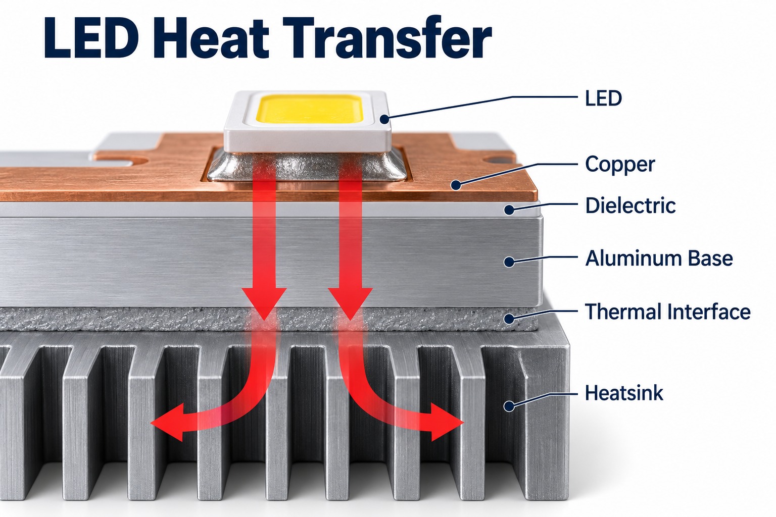
For thermal vias under power ICs, MOSFETs, LEDs, and heat-generating components, solid connection is usually better. These vias are used to transfer heat into inner copper planes or bottom copper areas. Thermal relief would reduce the heat path and weaken cooling performance.

Thermal relief can be useful when a via is also a solderable test point, jumper point, or hand-rework feature. In that case, solderability may matter more than maximum current or heat transfer. The via rule should always follow the via function.

PCB Thermal Relief Via Design, https://www.bestpcbs.com/blog/2026/06/pcb-thermal-relief/

When Should High-Current PCB Avoid Thermal Relief?

High-current PCB should avoid thermal relief when the connection must carry sustained current, spread heat, or keep impedance low. In these areas, solid copper usually gives safer electrical and thermal performance.

Avoid or limit thermal relief in these areas:

  • Power input terminals with sustained load current.
  • Battery connector pads where voltage drop is critical.
  • Motor driver outputs with high current pulses.
  • MOSFET drain pads used for heat spreading.
  • Power IC exposed pads that transfer heat to copper planes.
  • LED thermal pads on aluminum PCB or copper core PCB.
  • Copper bus bar connections and heavy copper paths.
  • RF ground pads where low impedance is important.
  • Thermal via arrays under hot components.

Thermal relief may still be used when soldering risk is higher than current risk, but the setting should be customized. Default narrow spokes are rarely suitable for demanding power circuits.
How to Balance Solderability and Current Capacity in High-Current PCB Thermal Relief?

High-current PCB thermal relief design should balance soldering quality, current capacity, voltage drop, and temperature rise. The goal is not to use thermal relief everywhere. The goal is to choose the copper connection that fits the working condition.

Use this decision logic:

  • Start from the current path.
    Identify where current enters, exits, and spreads through the copper plane. If the relief spokes become the narrowest part of the path, they may control the real current capacity.
  • Use solid connect when current is the main risk.
    If the pad carries sustained high current, pulse current, or heat from a power device, solid copper usually gives lower resistance and lower temperature rise.
  • Use thermal relief when soldering is the main risk.
    If the pad connects to a large plane and soldering is difficult, thermal relief may be useful. The spokes should be enlarged enough to avoid current bottlenecks.
  • Use wider or multi-spoke relief when both risks exist.
    For moderate-to-high current pads that are also hard to solder, use wider spokes, four spokes, or customized copper windows. This improves soldering while keeping more copper area.
  • Check voltage drop across the connection.
    Even a short spoke can add resistance if it is too narrow. In low-voltage power circuits, small voltage loss may affect efficiency, output stability, or thermal behavior.
  • Check temperature rise under real load.
    A layout may pass visual inspection but still create hot spots. For high-current boards, temperature rise should be checked by calculation, first article testing, or thermal measurement.
  • Match the choice with assembly method.
    Hand soldering, wave soldering, selective soldering, and reflow soldering do not behave the same. A pad that is easy to solder in reflow may still be difficult during manual repair.
  • Avoid using default CAD rules for power nets.
    Default relief settings are often created for general solderability, not sustained current. High-current nets should use separate design rules.

A good design keeps the joint solderable without turning the spokes into weak current paths. If current, heat, or mechanical stress is high, stronger copper should take priority.

PCB Thermal Relief Design, https://www.bestpcbs.com/blog/2026/06/pcb-thermal-relief/

Is There a PCB Thermal Relief Calculator for High-Current Design?

A PCB thermal relief calculator can be used as a reference for spoke current capacity, resistance, voltage drop, and temperature rise, but it cannot replace layout review or real-load testing. Thermal relief is not a simple straight trace because current spreads through pads, spokes, planes, solder, and nearby copper.

A useful calculation should include spoke width, spoke count, copper thickness, spoke length, current load, allowed temperature rise, copper weight, board material, airflow, and nearby copper area. The total copper cross-section of all spokes is more important than one single spoke width.

A practical workflow is simple. First, define the continuous current and peak current. Then check the copper thickness and available pad space. Next, estimate whether the total spoke width can carry the load with acceptable voltage drop. After that, review whether the same spoke setting still allows good solder wetting.

The calculator result should be treated as an early design check. For power terminals, motor control PCB, automotive PCB, LED PCB, heavy copper PCB, and copper bus connections, the final decision should include DFM review, first article inspection, soldering feedback, and thermal rise testing.

Common PCB Thermal Relief Mistakes in High-Current Circuits

The most common mistake is using default thermal relief settings on high-current pads. High-current PCB needs controlled copper connection rules because small layout details can affect current flow, heat rise, soldering, and reliability.

MistakeRiskSolution
Narrow spokes on power padsHot spots, voltage dropIncrease spoke width or use solid connect
Only two spokes on high-current padsUneven current distributionUse four spokes or custom copper connection
Thermal relief on thermal viasPoor heat transferUse solid via-to-plane connection
Same rule for all connector pinsWeak power pathSeparate rules by pin function
Oversized relief gapLong and weak spokesReduce gap or widen spokes
Ignoring copper thicknessWrong current estimateMatch relief settings with copper weight
Relief on MOSFET or LED thermal padsHigher device temperatureUse solid copper and thermal vias
No load testingHidden temperature riseTest first article under working current
Only focusing on solderabilityLong-term reliability riskCheck current, heat, and soldering together

A practical fix starts at the rule level. Create separate copper connection rules for signal nets, ground nets, power nets, thermal vias, connectors, and heavy copper areas. Then review high-current pads manually instead of relying only on automatic copper pour settings.

During production review, check Gerber data, copper thickness, spoke geometry, pad size, annular ring, soldering method, and expected load current. For critical boards, use thermal rise testing or current loading tests before mass production. This helps find hot spots before the product reaches the field.

FAQs About PCB Thermal Relief in High-Current PCB Design

Q1. Can a power connector use different copper rules on different pins?
A1. Yes. A power connector can use mixed copper rules by pin function. Signal pins may use normal relief, ground pins may use wider relief, and high-current power pins may use solid connect. This is often better than applying one setting to the whole connector footprint.

Q2. Why do high-current pads become hot even when the trace is wide enough?
A2. The pad connection may be the bottleneck. A wide trace does not help if current must pass through narrow thermal spokes before reaching the plane. Check spoke width, spoke count, gap, copper thickness, and the full current path from pad to copper area.

Q3. Is four-spoke thermal relief always suitable for power pads?
A3. No. Four spokes are better than two in many cases, but they may still be too narrow for high current. The total spoke width, copper thickness, current load, and temperature rise decide whether the design is safe. Some power pads still require solid copper.

Q4. Can solder added to the pad increase current capacity?
A4. Solder can add some conductive material, but it should not be used as the main current path. Copper carries current much better than solder. The PCB copper design should already support the required current before relying on solder thickness or solder fill.

Q5. Should battery pads use thermal relief?
A5. Battery pads usually need strong copper connection because voltage drop and heat rise are important. Thermal relief may help soldering, but default narrow spokes can reduce reliability. For battery input pads, solid connect or enlarged custom relief is often a safer choice.

Q6. How can I tell if a thermal relief setting is too weak?
A6. Warning signs include narrow spokes, long spokes, high load current, visible copper bottlenecks, or hot spots during testing. If the thermal image shows heat concentrated at the pad connection, the relief pattern may be too weak and should be widened or changed to solid connect.

Q7. Is thermal relief acceptable for screw terminal pads?
A7. It depends on current and soldering difficulty. Screw terminals often carry high current and face mechanical stress, so solid connect is common. If solder fill is difficult, use wider spokes or selective relief, but avoid thin spokes that weaken current capacity and pad strength.

Q8. Does heavy copper always solve thermal relief problems?
A8. No. Heavy copper helps current capacity, but the spoke geometry still matters. If the relief spokes are too narrow, they can still limit current. Heavy copper also pulls heat faster during soldering, so spoke width, gap, and assembly method must be reviewed together.

Q9. Can thermal relief be used in automotive high-current PCB?
A9. Yes, but it should be reviewed carefully. Automotive PCB may face vibration, temperature cycling, and sustained current. Thermal relief may be acceptable for soldering-sensitive pins, but power pads, relay outputs, motor lines, and thermal paths often need solid copper or enlarged connections.

Q10. What should be checked before sending high-current PCB files to production?
A10. Check current paths, copper thickness, spoke width, spoke count, gap, pad size, connector pin function, via connection, soldering process, and expected temperature rise. For power boards, also provide load current, working temperature, and heat-generating component details to the PCB manufacturer.

Q11. Why is thermal relief risky under MOSFET drain pads?
A11. MOSFET drain pads often use copper as both an electrical and thermal path. Thermal relief can restrict heat spreading and increase local temperature. For power MOSFET areas, solid copper, wide copper pours, and thermal via arrays are usually better for heat transfer.

Q12. What information helps a manufacturer review high-current thermal relief?
A12. Gerber files, stackup, copper thickness, BOM, current requirement, load condition, assembly method, and thermal notes are useful. These details help the manufacturer review whether power pads, connector pins, vias, and copper pours can support both soldering and long-term operation.

Conclusion

PCB thermal relief in high-current circuits should be selected by current capacity, heat transfer, solderability, and long-term reliability. Thermal relief can make power pads easier to solder, but narrow spokes may create voltage drop and heat rise under real load. For power terminals, high-current connectors, thermal vias, MOSFET pads, LED heat pads, and heavy copper paths, solid connect or enlarged spoke design is often safer.

The best design depends on copper thickness, spoke width, spoke count, gap, pad function, and assembly method. EBest Circuit is a China-based source PCB and PCBA manufacturer supporting custom fabrication, layout review, DFM checking, and global delivery. For high-current PCB thermal relief design review, prototype orders, or bulk PCB manufacturing, send your files and requirements to sales@bestpcbs.com.

You may also like

What is Routing in PCB? How to Properly Route a PCB?

June 10th, 2026

Routing in PCB is the process of creating copper trace paths that connect components, vias, pads, power nets and ground areas on a PCB. It decides how signals and current move across the board after schematic design and component placement are complete.

A good routing plan improves signal stability, reduces EMI risk, supports easier PCB manufacturing and helps prevent assembly defects. For custom PCB projects, routing is not only a design step. It also affects impedance control, soldering quality, testing yield, product reliability and final production cost.

Routing in PCB, https://www.bestpcbs.com/blog/2026/06/routing-in-pcb/

What is Routing in PCB?

Routing in PCB means building the physical copper connections between electrical nodes on a printed circuit board. The schematic shows which pins should connect, while routing defines how those connections travel through traces, vias and copper planes.

In PCB design, routing starts after component placement and rule setup. The designer selects trace width, trace spacing, via position, routing layer and return-current path based on electrical and manufacturing requirements.

For simple circuits, routing may only involve short signal traces and basic power paths. For high-speed, RF, dense BGA or power boards, routing in PCB becomes more important because signal timing, impedance, heat and noise must be controlled together.

Why Is Routing Important in PCB Design and Manufacturing?

Routing is important because it directly affects PCB signal quality, manufacturing yield, assembly reliability and long-term product performance. Poor routing can cause noise, voltage drop, unstable communication, EMI failure or repeated production rework.

In PCB design, routing controls signal path length, current capacity, crosstalk, impedance and ground return quality. In PCB manufacturing, routing also affects etching accuracy, solder mask clearance, drill reliability, copper balance and panel separation.

For production projects, routing problems often appear as random reset, weak RF signal, failed impedance testing, solder defects or unstable batch quality. Therefore, routing in PCB should be reviewed before fabrication files are released, not after defects appear in production.

What Are the Main Types of Routing in PCB?

The main types of routing in PCB include manual routing, auto routing, interactive routing, differential pair routing, serpentine routing, arc routing, point-to-point routing, daisy chain routing and star routing.

TypeUse CaseKey Concern
Manual routingCritical signals, high-speed nets, dense layoutsMore layout time
Auto routingSimple low-speed connectionsMust be reviewed manually
Interactive routingRule-guided trace routingDepends on correct rule setup
Differential pair routingUSB, Ethernet, HDMI, LVDS, PCIeImpedance and length matching
Serpentine routingLength matching for timing signalsAvoid excessive coupling
Arc routingRF, antenna, curved signal pathsKeep spacing and impedance stable
Point-to-point routingDirect two-node connectionsKeep the path short
Daisy chain routingMemory, LED, bus-style connectionsControl timing skew
Star routingPower or low-speed signal branchesKeep branches balanced

How Does the PCB Routing Process Work?

The PCB routing process turns schematic connections into copper traces that can be manufactured, assembled and tested reliably. A clear routing process reduces signal errors, DFM issues and production rework.

Step 1: Confirm the PCB stackup.
Check layer count, board thickness, copper weight, dielectric material and impedance requirements before routing. These factors decide trace width, routing layer, via type and reference plane quality.

Step 2: Set routing rules first.
Define trace width, trace spacing, via size, clearance, differential pair rules, length matching limits and high-voltage spacing in the design software. This prevents many routing errors before they happen.

Step 3: Optimize component placement.
Place connectors, ICs, decoupling capacitors and power components to shorten critical paths. Good placement reduces crossed traces, unnecessary vias and routing congestion.

Step 4: Route critical nets first.
Route clocks, RF lines, USB, Ethernet, LVDS, DDR, differential pairs, power rails and sensitive analog signals before low-speed nets. These lines have higher requirements for impedance, timing, noise control and return path continuity.

Step 5: Build stable power and ground paths.
Use enough trace width or copper area for power nets. Keep ground continuous under high-speed signals whenever possible, because broken return paths can cause EMI, signal distortion and unstable operation.

Step 6: Complete general signal routing.
Route low-speed control lines and ordinary signals after critical nets are complete. Keep traces clean, avoid unnecessary vias, reduce long parallel routing and leave enough clearance for solder mask and assembly.

Step 7: Review routing before production.
Run DRC, DFM, netlist comparison, impedance review, copper balance review, solder mask review and assembly clearance inspection. The PCB should enter fabrication only after routing errors and manufacturability risks are corrected.

 PCB Routing Process

What Routing Rules Should Be Followed in PCB Design?

PCB routing rules should control trace width, trace spacing, via size, impedance, clearance, length matching, copper balance and return-current path. These rules help the PCB stay reliable in both testing and mass production.

Important routing rules include:

  • Trace width: match current load, temperature rise and copper thickness.
  • Trace spacing: reduce short risk, crosstalk and high-voltage arcing.
  • Via design: avoid unnecessary vias on critical high-speed paths.
  • Impedance control: keep high-speed traces within required impedance range.
  • Length matching: control timing skew for sensitive signal groups.
  • Ground reference: route fast signals near a continuous ground plane.
  • Copper balance: reduce warpage during lamination and reflow.
  • Test access: keep important nets available for inspection and debugging.

PCB routing rules should match real factory capability. A layout may pass software checks but still cause low yield if trace spacing, annular ring, solder mask bridge or drill tolerance is too aggressive.

How to Properly Route a PCB?

To properly route a PCB, route important signals first, keep paths short, protect return current, control spacing and confirm manufacturability before releasing files. Proper PCB routing should support both electrical stability and production yield.
Step 1: Start with high-risk signals.
Route clocks, RF signals, differential pairs, high-speed buses and sensitive analog traces first. These signals are more likely to cause EMI, signal loss, timing errors or unstable communication if routed poorly.

Step 2: Keep traces short and direct.
Short traces reduce resistance, delay, noise pickup and unwanted antenna effects. Avoid long detours unless they are required for length matching, spacing or mechanical clearance.

Step 3: Keep a continuous ground reference.
High-speed traces should stay close to a solid ground plane. Avoid routing fast signals across ground splits, large cutouts or broken reference areas because this can disturb return current and increase EMI risk.

Step 4: Control trace width and spacing.
Choose trace width based on current load, impedance target, copper thickness and factory capability. Set proper spacing to reduce shorts, crosstalk and voltage clearance problems. Trace width should be calculated, not guessed.

Step 5: Use vias carefully.
Each via adds discontinuity, inductance and manufacturing tolerance risk. Use vias when layer changes are necessary, but keep critical high-speed routes as simple as possible.

Step 6: Route differential pairs correctly.
Keep the two traces close, symmetrical and length matched. Avoid sudden spacing changes, uneven vias and broken ground reference. For differential pair routing in PCB, stable impedance and clean return paths are more important than visual symmetry alone.

Step 7: Separate noisy and sensitive circuits.
Keep switching power traces, clock lines, RF routes and high-current paths away from sensitive analog signals. This reduces coupling noise, false readings and communication errors.

Step 8: Reserve space for manufacturing and assembly.
Check solder mask bridges, via-to-pad distance, annular ring, component spacing, panel edge clearance and test access. A properly routed PCB should be easy to fabricate, assemble, inspect and test.

Step 9: Check all files before Gerber release.
Review DRC, DFM, impedance notes, drill files, solder mask clearance, copper balance and test points. For BGA, fine-pitch ICs, RF or high-speed designs, factory review should happen before final production files are released.

PCB Routing

What Are Effective Routing Techniques in PCB Design?

Effective routing techniques in PCB design help signals move cleanly, reduce EMI, control heat and make the PCB easier to manufacture. Good routing is not only about connecting nets. It should also support stable testing, smooth assembly and reliable long-term operation.

  • Route critical signals first:
    Clocks, RF lines, USB, Ethernet, LVDS, PCIe, DDR and sensitive analog traces should be routed before normal low-speed nets. These signals are more sensitive to impedance, length, spacing and return-current path.
  • Keep traces short and direct:
    Short traces reduce resistance, delay, signal loss and unwanted antenna effects. Avoid long detours unless length matching, clearance or mechanical structure requires them.
  • Use a continuous ground reference:
    High-speed traces should stay close to a solid ground plane. A clean ground reference gives return current a stable path and helps reduce EMI, ringing and random communication errors.
  • Separate noisy and sensitive circuits:
    Switching power traces, clock lines, RF paths and high-current routes should stay away from analog, sensor and low-level signal traces. This reduces coupling noise and improves circuit stability.
  • Control power trace width:
    Power routes should be wide enough for the required current. In higher-current areas, wider traces, copper pours and multiple vias help reduce voltage drop and heat buildup.
  • Avoid long parallel routing:
    Long parallel traces can increase crosstalk, especially between high-speed or noisy signals. Keep enough spacing, change routing direction between layers where possible and avoid placing sensitive traces beside switching nodes.
  • Use vias carefully:
    Vias are useful for layer changes, but they add discontinuity and tolerance risk. On critical nets, reduce unnecessary vias. For differential pairs, keep vias balanced on both traces.
  • Route differential pairs as controlled pairs:
    USB, Ethernet, HDMI, LVDS and PCIe signals should keep stable spacing, matched length and a continuous reference plane. Stable impedance and clean return paths are more important than visual neatness.
  • Leave room for assembly and testing:
    Keep enough solder mask clearance, avoid vias too close to pads and reserve practical test points for important nets. A good routing layout should be easy to fabricate, assemble, inspect and repair.

How to Route Differential Pair Traces in PCB?

Differential pair routing in PCB should keep the two traces symmetrical, close together, length matched and referenced to a continuous ground plane. This helps maintain controlled impedance and stable signal transmission.

Differential pairs are used in USB, Ethernet, HDMI, LVDS, PCIe and many high-speed interfaces. The two traces should keep consistent spacing and avoid long separation. If one trace bends around an obstacle, the other trace should follow a similar path to reduce skew.

When changing layers, both traces should use matched vias and stay close to the same reference plane. Avoid excessive serpentine tuning because dense meanders can create unwanted coupling noise.

For fabrication, differential pair routing should include clear impedance requirements in the PCB notes. The factory can then confirm stackup, trace width, dielectric thickness and copper weight before production.

Which Layer Should You Route Differential Signals in PCB?

Differential signals should be routed on layers next to a continuous ground reference plane whenever possible. This improves impedance consistency, return-current control and EMI performance.

On a 4-layer PCB, differential signals are often routed on the top or bottom layer with an internal ground plane nearby. On 6-layer or higher boards, inner stripline routing may provide better shielding and more stable impedance.

The best routing layer depends on signal speed, stackup, connector position, via count and EMI target. For high-speed interfaces, unnecessary layer changes should be avoided because each via can add discontinuity.

Before routing starts, the differential pair layer should be confirmed with the stackup. Changing the layer after routing may force impedance recalculation, trace-width changes and layout rework.

How Does PCB Routing Affect Manufacturing and Assembly?

PCB routing affects manufacturing and assembly through etching accuracy, solder mask clearance, drill reliability, copper balance, panel strength, separation method and inspection access. A good route should be easy to fabricate, assemble, separate and test.

In routing in PCB manufacturing, very narrow traces and tight spacing increase etching difficulty. Small annular rings raise drill registration risk. Vias placed too close to pads may cause solder wicking unless via-in-pad is properly filled or capped.

Tab routing and break routing belong more to PCB panelization and separation than signal trace routing. Tab routing keeps PCB units connected in a production panel with small tabs, while break routing creates routed gaps or weak separation points for later board separation.

If tabs, mouse bites, routed gaps or V-cuts are placed too close to copper, components or board corners, depanelization may damage the PCB edge or nearby solder joints. Therefore, panel routing should leave enough edge clearance and should be reviewed before mass production.

During assembly, poor routing around thermal pads, copper pours and fine-pitch ICs can cause tombstoning, solder bridges, voiding or difficult inspection. Therefore, fabrication, assembly and panel separation risks should be checked together.

What Common PCB Routing Mistakes Should Be Avoided?

Common PCB routing mistakes include broken return paths, uncontrolled trace width, poor spacing, excessive vias, weak power routing and ignoring factory limits. These mistakes may cause EMI failure, unstable signals, soldering defects, low yield or costly redesign.

  • Routing high-speed traces across ground splits:
    This breaks the return-current path and can cause EMI, reflection or unstable communication. High-speed traces should stay over a continuous reference plane whenever possible.
  • Choosing trace width by guesswork:
    A trace that looks acceptable may still overheat or create voltage drop. Trace width should be based on current load, copper thickness, temperature rise and PCB factory capability.
  • Using too many vias on critical nets:
    Each via adds discontinuity, inductance and process tolerance risk. Too many vias can reduce signal quality, especially on RF, clock, USB, Ethernet and other high-speed routes.
  • Ignoring differential pair consistency:
    Differential pairs can fail when spacing changes suddenly, vias are unbalanced or one trace takes a much longer path. Length matching alone is not enough; spacing, impedance and reference continuity also matter.
  • Placing noisy traces near sensitive traces:
    Switching power, clock and high-current routes can inject noise into analog, sensor or RF circuits. This may lead to false readings, weak signals or random product failures.
  • Overusing serpentine routing:
    Serpentine routing helps with length matching, but excessive meanders can create extra coupling and noise. Use it only when timing control is required.
  • Routing too close to pads or board edges:
    Vias near pads may cause solder wicking. Traces close to board edges, tabs or routed gaps may be damaged during depanelization. Keep enough clearance for soldering, inspection and panel separation.
  • Skipping DRC and DFM review:
    A PCB may look complete but still contain spacing, solder mask, annular ring, impedance or assembly risks. Final files should pass both design-rule checks and manufacturability review before Gerber release.

Why Choose EBest for PCB Routing and Layout Support?

EBest supports PCB routing and layout review with China source factory manufacturing, custom PCB production, PCBA assembly, DFM feedback and global delivery. Our value is practical coordination between layout decisions and real production results.

EBest helps customers check trace spacing, via design, solder mask clearance, impedance notes, copper balance, panelization and assembly risks before fabrication. This helps reduce avoidable rework in prototypes, small-batch orders and volume production.

As a China-based source factory, EBest does not claim false overseas factories, local warehouses or branch offices. Instead, we support global customers through direct factory communication, OEM/ODM manufacturing, quality inspection and export delivery.

For projects involving routing in PCB, EBest can help turn layout files into manufacturable PCB and PCBA products with fewer production surprises.

PCB Routing and Layout

FAQs About Routing in PCB

Q1: What is the difference between PCB layout and PCB routing?
A1: PCB layout includes component placement, board outline, stackup, copper pours, mechanical clearance and routing. PCB routing is the part that creates copper trace connections between electrical nets. Good placement can greatly reduce routing difficulty, especially on dense PCB boards.

Q2: What is trace routing in PCB?
A2: Trace routing in PCB means creating copper paths that connect component pads, vias, power nets and signal nets. It directly affects signal quality, current flow, trace spacing, layer choice and manufacturability.

Q3: How to route PCB in Altium properly?
A3: To route PCB in Altium properly, set design rules before routing, including trace width, clearance, via size, differential pair rules, impedance requirements and length matching limits. Critical nets should be routed first, and the final layout should pass DRC and DFM review before production.

Q4: What is routing topology configuration in PCB design?
A4: Routing topology configuration in PCB design means choosing how one signal connects to one or multiple loads. Common options include point-to-point, daisy chain, star and branch routing. The correct topology depends on signal speed, timing requirement, load count and impedance control.

Q5: Is auto routing good enough for PCB design?
A5: Auto routing may work for simple low-speed nets, but it is not enough for high-speed, RF, BGA, power or differential-pair PCB projects. For production boards, manual or interactive routing is usually safer for critical nets.

Q6: What trace width should be used in PCB routing?
A6: Trace width depends on current, copper weight, temperature rise, impedance target and factory capability. Signal traces can be narrow, while power traces should be wider or supported by copper pours. For high-current paths, trace width should be calculated before routing because visual estimation can cause overheating risk.

Q7: Why should PCB traces avoid 90-degree corners?
A7: Many PCB designers avoid 90-degree corners because they can create less smooth geometry, slight impedance discontinuity and possible process concerns in fine routing. Modern factories can often manufacture them, but 45-degree or arc routing is still preferred for cleaner routing and better high-speed practice.

Q8: What is serpentine routing in PCB used for?
A8: Serpentine routing is used to add controlled trace length for timing-sensitive signals. It is common in DDR, differential pairs and high-speed bus routing. However, excessive serpentine routing can increase local coupling noise. The goal is controlled length matching, not filling empty board space.

Q9: What is arc routing in PCB?
A9: Arc routing uses smooth curved trace paths instead of sharp angled traces. It is often used in RF, antenna, high-frequency and compact PCB layouts. Arc routing may reduce abrupt direction changes, but it must still follow trace spacing, impedance and fabrication limits.

Q10: What is tab routing in PCB manufacturing?
A10: Tab routing keeps multiple PCB units connected in a production panel by using small tabs. These tabs are removed after assembly or fabrication. Good tab placement improves handling, while poor placement can create edge burrs, cracks or component stress.

Q11: What is break routing in PCB?
A11: Break routing creates routed gaps or weak separation points between boards in a panel. It helps separate individual PCB units after production. If break routing is too close to components, traces or corners, depanelization may damage the board.

Q12: Which layer do you route differential signal in PCB?
A12: Differential signals are usually routed on layers adjacent to a continuous ground plane. This helps control impedance, reduce EMI and keep the return path stable. For high-speed PCB designs, unnecessary layer changes should be avoided because vias can create signal discontinuity.

Q13: Can poor routing cause EMI problems?
A13: Yes. Poor routing can cause EMI when fast signals cross ground splits, run beside noisy nets, form large loops or lack a clean return path. Proper routing, grounding and spacing can reduce emission and susceptibility risks.

Q14: Why do differential pairs fail even when lengths match?
A14: Differential pairs can fail if impedance is uncontrolled, spacing changes too much, vias are unbalanced or the reference plane is broken. Length matching alone is not enough. A reliable pair should keep stable spacing, symmetry, return path and impedance across the whole route.

Q15: What makes a PCB routing supplier reliable?
A15: A reliable supplier should understand layout, fabrication, assembly and testing together. Buyers should check DFM feedback ability, controlled-impedance experience, BGA handling, differential pair review and quality inspection options. For custom PCB and PCBA projects, engineering feedback speed and factory capability are both important.

Conclusion

Routing in PCB is the key link between circuit design and reliable manufacturing. The core technical point is clear: trace width, spacing, layer choice, impedance, return path, via control and manufacturability must work together. A PCB that only connects electrically may still fail in EMI testing, assembly or long-term use.

For selection, choose routing methods based on signal speed, current load, density, layer count and reliability target. For purchasing, work with a PCB and PCBA supplier that can review routing, fabrication, assembly and testing risks together before production. If your project requires custom PCB manufacturing, PCB layout support, DFM review or PCBA assembly from a China source factory with global delivery, contact EBest Circuit for a fast quotation: sales@bestpcbs.com.

You may also like

How to Design PCB Bluetooth Antenna for Stable Wireless Performance?

May 26th, 2026

Is your PCB Bluetooth antenna giving the product stable 2.4GHz wireless performance after assembly? In Bluetooth and BLE devices, antenna layout affects connection range, signal strength, power efficiency, and pairing consistency in real use.

A PCB bluetooth antenna works together with the RF feed line, ground plane, matching circuit, enclosure, battery, and nearby metal parts. This guide explains how to choose antenna types, arrange the PCB layout, design trace antennas, reduce common mistakes, and test the board before production.

PCB Bluetooth Antenna, https://www.bestpcbs.com/blog/2026/05/pcb-bluetooth-antenna/

What is a PCB Bluetooth Antenna?

A PCB Bluetooth antenna is a wireless antenna formed on or mounted to a printed circuit board for Bluetooth or BLE communication. It usually works in the 2.4GHz ISM band and sends or receives radio-frequency energy through a designed radiating structure.

The antenna may be a copper trace, a compact chip antenna, or a module-based antenna area. Its performance depends on antenna shape, PCB layout, ground plane, surrounding components, and final product enclosure.

For small wireless products, the antenna is often one of the most sensitive areas of the layout. A small change near the antenna area can shift frequency response, reduce range, or make tuning more difficult.

How Does a Bluetooth PCB Antenna Work?

A Bluetooth PCB antenna works by converting high-frequency electrical signals into electromagnetic waves, then receiving those waves from nearby devices. In a real board, the antenna does not work alone. It is part of a complete RF path.

  • Bluetooth IC or module: Generates and receives the 2.4GHz RF signal.
  • RF feed line: Carries the signal from the chip or module to the antenna. It is normally designed as a 50-ohm controlled line.
  • Matching network: Uses small capacitors or inductors to tune impedance between the RF source and the antenna.
  • Antenna radiator: The copper trace or chip antenna structure that radiates energy into free space.
  • Ground plane: Acts as the antenna’s reference area and strongly affects efficiency.
  • Product enclosure: Plastic, metal, glass, battery position, cable routing, and hand placement can change final antenna behavior.

A stable antenna design balances these elements instead of treating the antenna as a separate copper shape.

What Are the Main Types of Bluetooth Antenna on PCB?

Bluetooth antenna on PCB designs can use several structures. The right choice depends on board size, cost target, available space, enclosure shape, and required wireless range.

  • PCB trace antenna: This is a copper pattern directly etched on the PCB. It has low material cost and works well when enough board space and clearance are available.
  • Inverted-F antenna, IFA: This common 2.4GHz antenna structure has a feed point and ground connection. It can offer a practical balance of size and performance.
  • Meandered inverted-F antenna, MIFA: This pattern folds the antenna trace to save space. It is widely used in compact Bluetooth and BLE devices.
  • Chip antenna: This is a small ceramic or multilayer component placed on the PCB. It saves board area, but still requires the correct ground area and matching design.
  • Module antenna area: Some Bluetooth modules include a built-in antenna. The host PCB must still follow the module maker’s keepout and placement rules.
  • External antenna connector: For longer range or challenging enclosures, a connector and external antenna may be used.
PCB Bluetooth Antenna, https://www.bestpcbs.com/blog/2026/05/pcb-bluetooth-antenna/

For many IoT, sensor, handheld, and wearable products, PCB trace antenna and chip antenna solutions are the two most common paths.

Bluetooth Chip Antenna vs PCB Antenna: Which Is Better?

Both antenna styles can work well when they are designed correctly. The better choice depends on product size, available layout area, cost plan, and tuning goals. A PCB antenna usually saves component cost, while a chip antenna can reduce occupied area.

Comparison ItemPCB Trace AntennaBluetooth Chip Antenna
Board SpaceRequires a defined edge area and clear keepout zoneUses less physical antenna area
BOM CostLower because the antenna is part of the copper patternHigher because it adds a discrete antenna part
Layout SensitivityVery sensitive to ground, copper, and nearby partsAlso sensitive, but vendor layout guidance helps
TuningMatching network is strongly recommendedMatching network is usually required
Range PotentialGood when layout and ground plane are well designedGood in compact layouts when placed correctly
Manufacturing ControlDepends on trace accuracy, stackup, copper, and solder maskDepends on placement accuracy and antenna part consistency
Best FitCost-focused BLE devices, tags, sensors, and modules with enough spaceWearables, small handheld devices, dense IoT boards, and space-limited designs

A practical selection starts with available board area. If the product has enough edge clearance, a trace antenna can be efficient and economical. If space is tight, a chip antenna may be easier to fit, but it still requires careful placement and final tuning.

What Are the Best Practices for Bluetooth Antenna PCB Layout?

Good Bluetooth antenna PCB layout starts before the board is routed. The antenna area, ground clearance, feed line, and nearby components should be planned during the first placement stage.

  • Place the antenna near the PCB edge. Edge placement helps the antenna radiate away from the board and product body.
  • Reserve a clean keepout zone. Keep copper, traces, vias, screws, shields, displays, batteries, and cables away from the antenna area.
  • Use a 50-ohm RF feed line. Confirm trace width, dielectric thickness, and reference ground with the PCB stackup.
  • Keep the feed line short and direct. Long or curved RF routes can add loss and mismatch.
  • Place matching parts close to the antenna feed. Leave pads for a pi-network or similar tuning structure.
  • Avoid routing under the antenna. Signal traces and copper pours below the radiator can disturb performance.
  • Control ground stitching near the RF path. Use vias to keep the RF return path stable, while keeping the antenna keepout clear.
  • Check enclosure and battery position early. A large battery, metal cover, or nearby cable can detune the antenna after assembly.
  • Follow the antenna maker’s reference layout. For chip antennas and modules, the reference board layout is often the safest starting point.
  • Build tuning samples before volume production. Real boards should be measured and adjusted before the design is locked.

How to Design PCB Bluetooth Antenna for Stable Wireless Performance?

A reliable antenna design starts before routing begins. The antenna shape matters, but it is only one part of the full RF path. Feed line impedance, ground plane, matching parts, PCB stackup, enclosure space, and nearby metal all influence final Bluetooth performance. For bluetooth pcb trace antenna design, the goal is to create a repeatable 2.4GHz structure that still performs well after assembly.

Step 1: Check the Available Space First
Start with the real product size, not only the PCB outline. Check where the battery, housing, display, screws, cables, and metal parts will sit. If the board has enough open edge space, a PCB trace antenna can work well. If the product is very compact, a chip antenna or Bluetooth module antenna may be easier to place.

Step 2: Choose the Right Antenna Type
Select the antenna based on board size, cost target, range requirement, and layout freedom. A trace antenna saves BOM cost and suits many BLE products. A chip antenna takes less board area but still requires correct clearance and tuning. A module antenna can simplify RF design, but the host PCB must follow the module layout guide.

Step 3: Place the Antenna at the Board Edge
The antenna should usually be placed at the PCB edge or corner. This helps it radiate away from the board and reduces interference from dense circuitry. Avoid placing it near batteries, metal shields, USB ports, large connectors, displays, or mounting screws.

Step 4: Reserve a Clear Keepout Area
The antenna zone should stay free from copper pour, signal traces, vias, test pads, and components. This rule should apply to related layers, not just the top layer. A clean keepout area gives the antenna more stable radiation space and reduces frequency shift after assembly.

Step 5: Route a Controlled 50-Ohm RF Feed Line
The RF feed line connects the Bluetooth chip or module to the antenna. It should be designed as a 50-ohm transmission line according to the PCB stackup. Keep it short, direct, and smooth. Avoid sharp corners, unnecessary vias, long detours, or routing through noisy circuit areas.

Step 6: Add a Matching Network
Leave a footprint for a matching circuit, usually a pi-network made with capacitors and inductors. This small area is very useful during tuning. Even if the first layout follows a reference design, the final housing, battery, and nearby components may still shift antenna performance.

Step 7: Control the Ground Plane Carefully
The ground plane is part of the antenna system. Keep a solid reference ground under the RF feed line, but do not pour copper into the antenna keepout zone. Ground stitching vias can be placed near the RF path to improve return current control, while the radiator area should remain clear.

Step 8: Follow the Reference Pattern Closely
For a PCB trace antenna, start from a proven 2.4GHz reference pattern. Do not casually shorten, stretch, rotate, or reshape the antenna trace. Small geometry changes can alter resonance. For chip antennas, follow the antenna supplier’s land pattern, clearance area, feed layout, and ground rules.

Step 9: Confirm PCB Stackup and Material Details
PCB thickness, dielectric constant, copper thickness, solder mask, and fabrication tolerance all affect antenna behavior. Keep the stackup consistent from prototype to production. If the reference antenna is designed with solder mask coverage, the manufactured board should follow the same condition.

Step 10: Test with the Complete Product
A board may perform well in open air but change after final assembly. Test the antenna with the housing, battery, display, cables, and mechanical parts installed. Measure return loss, impedance, range, and connection stability. Adjust the matching parts when required, then lock the final layout, stackup, and matching values for production.

What Does a Bluetooth Antenna on PCB Pattern Look Like?

A Bluetooth antenna on PCB pattern is usually placed at the edge or corner of the board. It may look like a straight copper strip, an L-shaped trace, an inverted-F structure, or a folded meander line.

A simple monopole pattern can be used when there is enough length and clearance. In compact boards, a meandered pattern is common because it folds the radiating path into a smaller area while still targeting the 2.4GHz band.

The visible shape is only part of the design. The ground plane beside the pattern, feed location, shorting point, keepout area, and dielectric environment all affect final behavior.

For chip antenna designs, the pattern may look simpler because the antenna body is a mounted component. However, the land pattern, ground clearance, feed trace, and matching network remain critical to performance.

In practical layout work, the antenna pattern should not be treated as decorative copper. It is an RF structure that must match the board, device size, and final product environment.

PCB Bluetooth Antenna, https://www.bestpcbs.com/blog/2026/05/pcb-bluetooth-antenna/

How Does PCB Material Affect Bluetooth Antenna Performance?

PCB material affects Bluetooth antenna performance through dielectric constant, thickness, loss, copper profile, and tolerance. At 2.4GHz, these factors can shift impedance and change antenna resonance.

Standard FR4 is widely used for many Bluetooth and BLE products. For compact or more performance-sensitive designs, tighter stackup control and stable material data can make tuning easier.

Solder mask also changes the environment around a copper trace antenna. Some reference antennas specify whether the antenna trace is covered or exposed, so the manufactured board should follow the approved design closely.

Material choice alone does not create a strong antenna. Stable fabrication, controlled trace geometry, consistent board thickness, and proper assembly are just as important.

What Mistakes Should You Avoid in Bluetooth PCB Antenna Design?

Many Bluetooth antenna problems come from layout shortcuts rather than from the antenna type itself. Early planning helps prevent weak signal, short range, unstable connection, and late tuning changes.

  • Placing metal too close to the antenna: Batteries, shields, screws, connectors, and cables can absorb or disturb RF energy.
  • Ignoring the keepout area: Copper pours, vias, and traces in the antenna zone can change resonance.
  • Using a random antenna pattern: A copied pattern may fail if the board size, material, or ground plane is different.
  • Skipping the matching network: Without tuning parts, it becomes harder to correct mismatch after prototype testing.
  • Routing the RF feed like a normal signal trace: The RF line should be treated as a controlled transmission line.
  • Changing stackup after antenna design: Thickness or dielectric changes can affect impedance and tuning.
  • Testing only the bare board: The final enclosure, battery, display, cable, and nearby hand position can change performance.
  • Placing the antenna deep inside the PCB outline: Center placement usually limits radiation and increases coupling with other circuits.
  • Starting production before RF validation: Prototype measurement gives useful data before large batch manufacturing.

How to Test and Tune a PCB Bluetooth Antenna?

Testing and tuning help confirm whether the antenna works as expected in the real device. A design that looks correct in layout software still requires physical measurement, because RF behavior changes with assembly and enclosure details.

Step 1: Check the PCB layout before fabrication
Review antenna position, feed width, ground clearance, keepout, stackup, and matching pads. This step helps catch visible layout issues before boards are made.

Step 2: Measure impedance and return loss
Use a vector network analyzer to check the antenna around the 2.4GHz band. S11 and return loss data show how much RF energy is reflected back instead of radiated.

Step 3: Adjust the matching network
Change capacitor or inductor values in the matching circuit to bring the antenna closer to the desired impedance range. This is where reserved matching pads provide real design flexibility.

Step 4: Test with the full enclosure
Measure again after adding housing, battery, display, and mechanical parts. This gives a more realistic view of final performance.

Step 5: Run wireless range checks
Test connection stability at different distances, orientations, and product positions. BLE devices may also require checks under low-power operating modes.

Step 6: Prepare the production build record
Once tuning is complete, lock the antenna area, matching values, material stackup, and assembly notes for consistent manufacturing.

Where Is a PCB Bluetooth Antenna Commonly Used?

Bluetooth antennas on PCB are widely used in compact wireless products that require short-range communication, low power use, and convenient connection with phones, gateways, sensors, or control units.

  • IoT sensors: Temperature sensors, humidity sensors, asset trackers, and smart meters.
  • Wearable devices: Fitness bands, healthcare monitoring devices, and portable electronics.
  • Medical electronics: Handheld instruments, monitoring modules, and connected diagnostic devices.
  • Industrial control devices: Wireless control boards, data collection modules, and machine-side sensor nodes.
  • Smart home products: Locks, switches, thermostats, lighting controllers, and appliance modules.
  • Consumer electronics: Audio accessories, remote controls, game peripherals, and personal devices.
  • Automotive accessories: Bluetooth control modules, diagnostic dongles, and in-cabin wireless devices.
  • Lighting systems: BLE lighting controls, dimmers, sensor nodes, and smart LED modules.

How to Choose a Reliable PCB Bluetooth Antenna Manufacturer?

A reliable manufacturer should understand that a Bluetooth antenna area is part of the RF system, not just another copper feature. The fabrication process must support stable dimensions, clean etching, controlled stackup, and careful review before production.

  • DFM review for antenna areas: The supplier should check spacing, copper clearance, solder mask, edge clearance, and possible manufacturing risks.
  • Controlled impedance support: RF feed lines should be reviewed according to the confirmed stackup.
  • Stable PCB material and thickness control: Consistent dielectric thickness helps keep RF behavior more repeatable.
  • Accurate etching capability: Antenna traces and feed lines require clean geometry.
  • Prototype and small-batch support: Early samples help verify layout and tune matching values before larger orders.
  • PCBA assembly capability: Antenna tuning parts, RF chips, modules, and small passive components require controlled assembly.
  • Testing coordination: The manufacturer should support electrical testing and work smoothly with RF validation plans.
  • Traceability and quality records: Lot control, material records, and inspection data help maintain consistency across batches.
  • Experience with wireless products: Prior work with BLE, IoT, RF modules, sensors, and compact electronics is valuable.
PCB Bluetooth Antenna, https://www.bestpcbs.com/blog/2026/05/pcb-bluetooth-antenna/

FAQs About PCB Bluetooth Antenna

Q1: Can Bluetooth use a PCB trace antenna instead of an external antenna?
A1: Yes. A PCB trace antenna can support Bluetooth and BLE communication when the layout is designed for the 2.4GHz ISM band. It is often used in sensors, smart home products, handheld devices, and compact wireless modules because it saves component cost and does not require an external antenna connector.

Q2: What frequency should a Bluetooth antenna on PCB support?
A2: A Bluetooth antenna on PCB should work around 2.4GHz to 2.4835GHz. This is the standard Bluetooth operating band. The antenna pattern, feed line, ground plane, and matching network should all be designed around this frequency range.

Q3: Is a chip antenna always better than a PCB antenna?
A3: Not always. A chip antenna is useful when board space is limited, but it still needs proper clearance, ground design, and tuning. A PCB trace antenna can be a better choice when the board has enough edge space and the project needs lower BOM cost. Both antenna styles usually need a 50-ohm RF feed line and a matching circuit.

Q4: How much clearance should be kept around a Bluetooth PCB antenna?
A4: Clearance depends on the antenna type and reference design. As a practical rule, the antenna area should be free from copper, vias, batteries, cables, shields, screws, and large metal parts. Many 2.4GHz antenna layouts require several millimeters of keepout, and some designs may require 5mm to 15mm or more depending on the structure.

Q5: Why does Bluetooth signal become weaker after the product is assembled?
A5: The antenna environment changes after assembly. Plastic housing, battery position, display modules, metal clips, charging cables, and hand contact can shift antenna tuning. That is why testing should be done with the complete product, not only the bare PCB. A design that works in open air may perform differently after final assembly.

Q6: Does PCB material affect Bluetooth antenna performance?
A6: Yes. PCB thickness, dielectric constant, copper thickness, solder mask, and manufacturing tolerance can affect antenna resonance and impedance. Standard FR4 is widely used for Bluetooth products, but stable stackup control is important. At 2.4GHz, even small changes in dielectric thickness or copper geometry can influence tuning.

Q7: Should the Bluetooth antenna trace be covered with solder mask?
A7: It depends on the reference design. Some antenna patterns are designed with solder mask coverage, while others require exposed copper. If the prototype antenna is tuned with solder mask coverage, the production PCB should keep the same condition to avoid frequency shift.

Q8: Why is a matching network required for a PCB antenna?
A8: A matching network helps tune the impedance between the RF circuit and the antenna. It usually uses small capacitors and inductors, often arranged as a pi-network. This allows the antenna to be adjusted after real-board testing. For Bluetooth designs, the RF path is commonly designed around 50 ohms.

Q9: Can the Bluetooth antenna be placed anywhere on the PCB?
A9: No. The antenna is usually placed at the PCB edge or corner to improve radiation. Placing it near the center of the board, close to a battery, under a display, or beside metal shielding can reduce wireless range. A clean edge location gives the antenna a better chance to radiate outward.

Q10: What should be checked before producing a Bluetooth antenna PCB?
A10: Before fabrication, check the antenna pattern, keepout area, RF feed width, ground plane, matching pads, PCB stackup, solder mask condition, and enclosure distance. For better production consistency, the final tuned design should lock the stackup, antenna geometry, and matching component values before batch manufacturing.

Conclusion

A PCB Bluetooth antenna can deliver stable wireless performance when the RF path, antenna area, ground reference, material stackup, and tuning process are planned together. The best results usually come from early layout discipline, controlled prototype builds, and real-device testing before production.

If you are preparing a Bluetooth, BLE, IoT, sensor, medical, industrial control, lighting, or compact wireless PCB project, EBest Circuit can support PCB fabrication(including FR4 PCB, RF circuit boards and so on), DFM review, controlled impedance guidance, PCBA assembly, component sourcing, and production-quality support. Send your Gerber files, stackup requirements, BOM, and product specifications to sales@bestpcbs.com for a quotation and technical review.

You may also like

Microphone PCB Design, Prototype & Assembly | One Stop Solutions

May 26th, 2026

How can a microphone PCB support clearer sound, lower noise, and more stable production? In audio devices, voice control modules, intercom systems, medical electronics, automotive voice units, and industrial acoustic equipment, the board plays an important role in signal transfer and assembly quality.

A well-planned microphone PCB helps control routing, grounding, power stability, microphone placement, and acoustic alignment. This guide explains board types, layout methods, mounting steps, prototype checks, assembly control, testing, and custom manufacturing support from EBest.

Microphone PCB, https://www.bestpcbs.com/blog/2026/05/microphone-pcb/

What Is a Microphone PCB Board?

A microphone PCB board is a printed circuit board used to mount microphone parts and connect them with the rest of an electronic product.

It may carry a MEMS microphone, condenser microphone capsule, electret microphone, preamp circuit, filtering parts, connector, power circuit, and test points. In some products, the board is very small. In others, it may be part of a larger audio, control, or communication system.

Its main job is to help the sound signal move from the microphone element to the processing circuit. Since this signal is usually weak at the beginning, the board layout should reduce noise, protect the input path, and keep power stable.

A good microphone board should also match the product structure. The acoustic hole, connector direction, screw holes, board outline, gasket position, and housing opening should all be checked before production.

What Types of Microphone PCB Boards Are Commonly Used?

Different audio products use different microphone board structures. The right choice depends on the microphone element, signal output, available space, acoustic design, and assembly method.

  • Condenser Microphone PCB
    A condenser microphone PCB is often used in recording devices, communication equipment, studio microphones, and professional audio products. It usually supports bias voltage, impedance conversion, signal filtering, and low-noise routing.
  • MEMS Microphone PCB Board
    MEMS microphone boards are widely used in earbuds, smart speakers, wearable devices, IoT products, and compact voice modules. This type usually requires SMT assembly, accurate acoustic hole alignment, and controlled reflow soldering.
  • Electret Microphone PCB Board
    An electret microphone PCB board is common in headsets, intercom systems, toys, small audio modules, and simple voice pickup devices. It usually includes a bias resistor, coupling capacitor, connector, and basic filtering circuit.
  • Analog Microphone PCB
    An analog microphone board sends a continuous analog signal to the next audio circuit. It is often used in products that require simple signal processing, flexible circuit adjustment, or traditional audio input design.
  • Digital Microphone PCB
    A digital microphone board is often used with MEMS microphones that output digital signals such as PDM or I²S. It is suitable for compact smart devices where space-saving layout and stable digital signal routing are important.
  • Microphone Array PCB
    A microphone array board uses two or more microphones on one PCB to improve voice pickup direction, noise reduction, or far-field sound capture. It is commonly used in smart speakers, conference systems, automotive voice modules, and voice control devices.
Microphone PCB, https://www.bestpcbs.com/blog/2026/05/microphone-pcb/

What Are Best Practices for Microphone PCB Layout?

Good layout helps protect weak audio signals from noise, unstable power, and unwanted interference. In a microphone circuit, the input signal is usually very small before amplification, so routing, grounding, component placement, and acoustic structure should be planned carefully from the beginning.

  • Keep microphone input traces as short as possible
    The trace from the microphone output to the first amplifier, codec, ADC, or connector should be short and direct. Long traces can act like antennas and pick up noise from nearby power, RF, clock, or digital circuits.
  • Separate audio traces from noisy circuits
    Microphone signal traces should stay away from switching regulators, wireless modules, crystal clocks, motor drivers, LED drivers, USB lines, and other high-speed or high-current areas. If the board space is limited, place the microphone circuit in a quieter area of the PCB.
  • Use a clean and stable ground path
    A poor ground path may create hum, noise, or unstable signal levels. For analog microphone circuits, keep the return path short and predictable. Avoid forcing low-level audio signals to share the same ground return path with noisy power circuits.
  • Place decoupling capacitors close to active components
    Power filtering parts should be placed near microphone ICs, preamp ICs, codecs, and ADCs. This helps stabilize the supply voltage and reduce power ripple before it reaches sensitive audio circuits.
  • Keep high-impedance areas clean and protected
    Condenser and electret microphone circuits may include high-impedance input areas. These areas should be short, clean, and away from contamination-prone zones. Flux residue, moisture, or dust may affect signal stability in sensitive designs.
  • Avoid routing noisy traces under the microphone section
    Clock lines, high-speed digital traces, RF lines, and switching power traces should not pass under the microphone input circuit or sound port area. If crossing is unavoidable, use proper layer planning and grounding to reduce coupling.
  • Plan the acoustic opening with the layout
    The sound port, PCB hole, gasket, enclosure opening, and microphone position should align accurately. A good electrical layout may still perform poorly if the acoustic path is blocked, shifted, or poorly sealed.
  • Leave enough space for assembly and inspection
    Do not place tiny passive parts too close to the microphone port, connector edge, or enclosure wall. Keep enough clearance for SMT placement, solder paste printing, AOI inspection, hand soldering when required, and fixture testing.
  • Add test points where they are useful
    Test points for power, ground, signal output, and control lines can make prototype validation and production testing easier. They should be placed where test probes can access them without touching sensitive microphone parts.
  • Match the layout with the final housing
    A microphone board is often used inside a compact product. Board outline, connector direction, screw holes, acoustic hole, cable exit, and enclosure clearance should be reviewed together before fabrication.

How Should a Microphone PCB Be Mounted?

Mounting is not only a mechanical step. It affects soldering quality, sound pickup, acoustic sealing, enclosure fit, and long-term reliability. Before mounting a microphone PCB, the microphone type, sound port direction, board outline, gasket position, and housing opening should be checked together.

Step 1: Confirm the microphone package and port direction
First, check whether the microphone is MEMS, condenser, electret, SMD, through-hole, top-port, or bottom-port. A top-port microphone receives sound from the top side of the part, while a bottom-port microphone receives sound through a hole in the PCB. This difference directly affects board hole design and enclosure alignment.

Step 2: Review the footprint and pad design
The land pattern should follow the component datasheet and assembly process. Pad size, solder mask opening, stencil aperture, and spacing should be checked before production. An unsuitable footprint may cause solder bridging, weak solder joints, floating parts, or placement shift.

Step 3: Align the acoustic hole correctly
For a bottom-port microphone, the PCB hole must align with the microphone sound inlet. The hole should not be blocked by solder mask, copper, adhesive, gasket material, or enclosure ribs. For a top-port microphone, the housing opening should sit directly above the sound port.

Step 4: Control solder paste volume
Solder paste should be controlled carefully around microphone pads. Too much solder may lift the part, affect sealing, or create bridging. Too little solder may reduce joint strength. For MEMS microphones, stencil design and reflow control should follow the part supplier’s recommendations.

Step 5: Match the board with the enclosure
The PCB should fit the final housing without stress. Screw holes, clips, posts, connectors, cable exit, gasket, and sound opening should be checked as one structure. If the board is bent or pressed after installation, solder joints and microphone performance may be affected.

Step 6: Use proper gasket or sealing design when required
Many microphone products use a rubber gasket or acoustic sealing structure between the board and housing. The gasket should guide sound into the microphone port without air gaps, compression loss, or misalignment. Poor sealing can reduce sensitivity or cause inconsistent sound pickup.

Step 7: Protect the sound port during assembly
Dust, solder balls, flux, cleaning liquid, adhesive, and coating material should not enter the microphone opening. If conformal coating or cleaning is used on the PCBA, the microphone area should be protected according to the process requirement.

Step 8: Avoid mechanical stress after mounting
Do not place screws, clips, or housing pressure points too close to the microphone part unless the structure has been verified. Mechanical stress may cause board warpage, solder joint strain, or acoustic leakage.

Step 9: Inspect the mounted board before testing
After assembly, check the solder joints, port alignment, board seating, gasket position, connector orientation, and housing fit. Visual inspection and basic electrical checks should be completed before sound-related testing.

Step 10: Run a functional sound check when required
For finished microphone PCB assemblies, a functional test can check power, signal output, noise level, sensitivity, or basic pickup response. This helps confirm that both the electrical path and acoustic path are working properly.

What Are Common Challenges in Microphone PCB Design and How Can They Be Solved?

Microphone circuits work with small signals, so board design should control noise, grounding, placement, power, and mechanical fit from the beginning.

  • Noise from nearby circuits
    Keep the input path away from RF, switching power, clock, and high-current areas. Add proper filtering and grounding.
  • Weak signal stability
    Use short routing, stable power rails, and close power filtering near active parts.
  • Hum from poor grounding
    Plan ground return paths carefully and avoid sharing noisy current paths with low-level audio signals.
  • Wrong sound port position
    Check microphone direction, PCB hole, gasket, and enclosure opening before fabrication.
  • Limited board space
    Use compact placement while keeping enough room for test pads, connector access, and assembly clearance.
  • Preamp sensitivity
    Keep the input area clean, reduce trace length, and separate the gain stage from noisy circuits.
  • Wrong surface finish or board thickness
    Choose board thickness and finish based on assembly, storage, connector type, and final housing structure.
  • Production variation
    Use DFM review before fabrication to check spacing, pad size, drill size, solder mask clearance, and assembly feasibility.

How Can Microphone PCB Prototyping Reduce Design and Assembly Risks?

Prototype production helps verify the circuit, structure, assembly process, and sound path before larger production begins. It is a practical way to find issues early.

  • Circuit verification
    A prototype can reveal gain issues, noise, wrong part values, unstable power, or signal path errors.
  • Housing fit check
    Board outline, screw holes, connector position, sound hole, and cable direction can be checked with the real enclosure.
  • Sound pickup review
    Teams can test signal level, sensitivity, noise behavior, and basic audio quality.
  • SMT process review
    Prototype assembly helps confirm solder paste, placement accuracy, reflow result, and port protection.
  • BOM review
    Microphone parts, preamp ICs, connectors, resistors, capacitors, and replacement choices can be checked early.
  • Test pad validation
    Test points and fixture access can be adjusted before the final production version.
  • Lower rework risk
    Finding issues during prototype work is easier than changing the board after larger assembly batches.

What Should Be Controlled During Microphone PCB Assembly?

Assembly control is important because microphone components may be sensitive to heat, dust, solder residue, and mechanical stress. A stable process helps improve repeatability.

  • Solder paste printing
    Stencil thickness and aperture design should match pad size and microphone package requirements.
  • SMT placement accuracy
    Placement should be controlled for MEMS microphones, ICs, connectors, and small passive parts.
  • Sound port protection
    The microphone port should be kept free from solder paste, dust, flux, and cleaning residue.
  • Reflow temperature profile
    The temperature curve should match solder paste requirements and component limits.
  • Part sourcing control
    Microphone parts, ICs, resistors, capacitors, and connectors should match the BOM and approved replacement list.
  • Connector soldering
    Board-to-board connectors, cable connectors, and wire harness areas should be checked for alignment and strength.
  • AOI inspection
    AOI can detect missing parts, wrong polarity, shifted components, and solder issues.
  • Functional test
    The assembled board can be checked for power, signal output, noise level, and basic microphone response when required.
Microphone PCB, https://www.bestpcbs.com/blog/2026/05/microphone-pcb/

What Quality Control and Testing Standards Are Used for Microphone PCB Production?

Quality control for microphone PCB production should cover bare board fabrication, material checking, SMT assembly, soldering quality, cleanliness, electrical performance, and functional testing. Since microphone circuits handle weak signals, small defects in routing, soldering, grounding, or acoustic alignment may affect final sound pickup.

  • DFM Review Before Production
    Before fabrication starts, Gerber files, drill files, solder mask openings, pad sizes, spacing, board outline, acoustic holes, and connector areas should be reviewed. This helps reduce layout risks before the board enters production.
  • Incoming Material Inspection
    PCB laminate, copper foil, solder mask, surface finish, solder paste, microphone parts, ICs, connectors, and passive components should be checked before use. For audio boards, part consistency and correct BOM matching are important.
  • Bare Board Electrical Testing
    The finished bare board should be tested for open circuits and short circuits. This step confirms that the copper traces and connections match the design before assembly.
  • Visual Inspection and AOI
    After SMT assembly, AOI can check missing parts, wrong polarity, shifted components, solder bridging, insufficient solder, and other visible assembly defects. This is especially useful for MEMS microphones, small resistors, capacitors, and fine-pitch ICs.
  • Soldering Quality Inspection
    Solder joints should be checked according to accepted PCBA workmanship standards, such as IPC-A-610 and J-STD-001 when applicable. The focus is solder wetting, joint shape, component alignment, bridging, tombstoning, and solder residue.
  • X-Ray Inspection When Required
    X-ray inspection may be used for hidden solder joints, bottom-terminated components, BGA packages, or dense assembly areas. It helps find voids, bridges, and poor solder connections that cannot be seen from the surface.
  • Cleanliness Control
    Microphone boards should be kept clean around microphone ports, high-impedance input areas, and acoustic openings. Flux residue, dust, cleaning liquid, or solder balls near the sound port may affect signal stability or acoustic performance.
  • Functional Electrical Testing
    The assembled board can be powered and checked for voltage, current, signal output, grounding, and basic circuit function. For microphone circuits, the signal path from microphone input to output connector or processing circuit should be verified.
  • Audio or Acoustic Function Test
    When required, the board can be tested for microphone response, noise level, sensitivity, signal level, or basic sound pickup. This test helps confirm that both the electrical path and acoustic path are working correctly.
  • Reliability Testing for Specific Applications
    Some projects may require thermal cycling, vibration testing, humidity testing, drop testing, or aging tests. These checks are often used when the board will work in automotive, medical, industrial, or outdoor electronic products.
  • Compliance and Process Standards
    Common references may include IPC-A-600 for bare PCB quality, IPC-A-610 for assembled board acceptance, J-STD-001 for soldering process control, RoHS for restricted substances, and ISO 9001-based quality management.
  • Traceability Records
    Production records, material batch information, inspection results, test data, and assembly process details should be kept for repeat orders and quality review. This is helpful when the same microphone board moves from prototype to mass production.

How Do You Choose a Reliable Microphone PCB Manufacturer?

A reliable supplier should understand fabrication, assembly, part sourcing, testing, and production communication. For audio boards, the supplier should also pay attention to low-level signal routing, acoustic holes, and component handling.

  • Fabrication capability
    The supplier should support standard FR4, multilayer boards, thin boards, impedance-related boards, and other board structures when required.
  • Assembly capability
    SMT assembly, connector soldering, inspection, and testing support help deliver a finished PCBA.
  • DFM review
    A useful supplier will review files before production and point out risks in pads, spacing, holes, solder mask, or assembly areas.
  • Component sourcing support
    Microphones, preamp ICs, connectors, and passive parts should be sourced with clear part matching and supply control.
  • Prototype and mass production support
    Early builds and larger production should both be supported by the same production flow when possible.
  • Delivery support
    Ask about prototype lead time, assembly lead time, and urgent order service when schedule matters.
  • Testing ability
    Bare board testing, AOI, X-ray when required, and functional checks can improve production confidence.
  • Clear communication
    Fast feedback on Gerber files, BOM issues, replacement parts, and delivery dates helps keep the project moving.

Why Choose EBest for Microphone PCB Design, Prototype, and Assembly?

EBest Circuit supports one-stop PCB and PCBA service, including PCB design, PCB prototype, mass production, component sourcing, and PCB assembly. The company was founded on June 28, 2006, and has more than 20 years of experience in PCB solutions. Here are reasons why choose EBest for microphone PCB manufacturer:

  • Design support before production
    EBest can review manufacturability, layout risks, pad design, drilling, spacing, solder mask, and assembly requirements before fabrication.
  • Prototype fabrication
    Prototype builds help verify circuit function, board fit, sound path, assembly process, and test access.
  • Mass production support
    EBest supports repeat production for audio, communication, industrial, medical, automotive, and smart electronics projects.
  • Component sourcing
    Microphones, ICs, connectors, resistors, capacitors, and related parts can be sourced together with assembly service.
  • PCB assembly
    SMT assembly, soldering, inspection, and testing help turn bare boards into functional PCBA products.
  • Wide board capability
    EBest’s product range includes FR4 PCB, multilayer PCB, metal core PCB, ceramic PCB, flexible and rigid-flex PCB, high frequency PCB, HDI PCB, heavy copper PCB, high-speed PCB, and impedance control PCB.
  • Fast delivery support
    EBest provides urgent board service, with some urgent boards shipped within 24 hours when project conditions allow.
  • Quality support
    The listed certifications include ISO 9001:2015, ISO 13485:2016, IATF 16949, AS9100D, REACH, RoHS, and UL.
  • What EBest can provide
    EBest can provide PCB design support, prototype fabrication, mass production, component sourcing, PCB assembly, DFM review, material suggestion, surface finish selection, testing, and production follow-up.
Microphone PCB, https://www.bestpcbs.com/blog/2026/05/microphone-pcb/

FAQs About Microphone PCB Board

Q1: What should be checked before designing a PCB mount microphone Board?
A1: For a PCB mount microphone Board, the sound port direction, pad size, solder paste opening, acoustic hole, and enclosure opening should be checked together. If the microphone is bottom-port, the PCB hole must align with the sound inlet. If it is top-port, the housing opening should sit above the microphone.

Q2: Why is a microphone preamp PCB important in audio products?
A2: A microphone preamp PCB boosts the weak microphone signal before it reaches an audio processor, ADC, codec, mixer, or control circuit. Good preamp layout helps reduce noise, stabilize gain, and improve signal clarity before later processing.

Q3: What makes a vintage microphone PCB different from a modern microphone board?
A3: A vintage microphone PCB is usually made for restoration, repair, or circuit replacement. It often has to match the original capsule type, board shape, connector location, and circuit style. Modern boards usually focus more on compact layout, SMT assembly, and stable production.

Q4: What information should be prepared before ordering a microphone board prototype?
A4: Gerber files, BOM, board thickness, copper weight, surface finish, quantity, assembly notes, microphone part number, datasheet, and test requirements are useful. If the board has an acoustic hole or special enclosure fit, those details should also be included.

Q5: Why does microphone board layout affect sound quality?
A5: Microphone signals are weak before amplification, so long traces, unstable grounding, nearby switching power circuits, RF lines, or poor filtering may add noise. Short input routing, clean ground paths, and proper circuit separation can improve sound pickup stability.

Q6: Can MEMS and condenser microphone boards use the same layout method?
A6: Not exactly. MEMS microphone boards often focus on SMT placement, acoustic port alignment, and compact routing. Condenser microphone boards usually require more attention to bias voltage, high-impedance input areas, low leakage paths, and analog signal cleanliness.

Q7: What tests are useful after microphone board assembly?
A7: Common checks include visual inspection, AOI, electrical testing, power-on testing, signal output checks, and basic sound pickup testing. For more demanding products, noise level, sensitivity, humidity, vibration, or aging tests may also be required.

Q8: What surface finish is commonly used for microphone boards?
A8: ENIG, OSP, and HASL may be used depending on pad design, storage time, assembly method, and product requirements. ENIG is often selected for fine-pitch parts or flatter soldering pads, while OSP and HASL may suit simpler board designs.

Q9: Can one supplier handle fabrication, parts sourcing, and assembly for microphone boards?
A9: Yes. For production projects, combining PCB fabrication, component sourcing, SMT assembly, inspection, and testing can make the process smoother. It also helps reduce file transfer mistakes, BOM mismatch, and production communication delays.

How Can You Get a Fast Quote for a Custom Microphone PCB?

Your microphone board deserves more than basic fabrication. If your project involves microphone PCB design review, prototype fabrication, component sourcing, SMT assembly, functional testing, or mass production, EBest can help turn your design files into a production-ready board with better control over layout details, acoustic alignment, soldering quality, and delivery schedule.

Send your Gerber files, BOM, quantity, microphone part details, and assembly requirements to sales@bestpcbs.com. Our team will review your files quickly and provide a clear quotation for your custom microphone PCB fabrication and assembly.

You may also like