PCB manufacturing PCB manufacturing
Home > Blog

High Speed PCB Design Guide for Signal Integrity and Manufacturability

August 28th, 2026

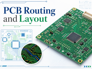
High speed PCB design is the discipline of controlling how fast signal edges travel through a real interconnect. A successful board needs more than clean routing: the stackup, dielectric system, trace geometry, reference planes, vias, connectors, power distribution network, and fabrication tolerances must work as one electrical structure.

This guide explains the decisions that should be settled before routing, the checks that protect signal and power integrity, and the manufacturing information a PCB supplier needs. The goal is not to promote one universal spacing or length rule. It is to show how interface requirements become a controlled, testable board construction.

High Speed PCB Design for signal integrity, power integrity, and manufacturability

What Is High Speed PCB Design?

High speed PCB design begins when an interconnect can no longer be treated as an ideal wire. During a fast transition, the trace, return plane, vias, pads, connectors, and package behave as a transmission path with distributed inductance, capacitance, resistance, and dielectric loss.

The important design questions are therefore electrical and physical at the same time:

  • Will the channel maintain the required characteristic impedance?
  • Can return current follow the signal without crossing a plane split or large discontinuity?
  • Are insertion loss, reflection, crosstalk, jitter, and skew within the interface budget?
  • Can the selected material, stackup, via structure, and trace geometry be manufactured repeatedly?
  • How will the finished board be tested against the released requirements?

When Does a PCB Signal Become High Speed?

A signal becomes a high-speed layout problem when its transition time is short enough for the physical interconnect delay to matter. Clock frequency alone is not a reliable boundary. A moderate-frequency clock with a sharp edge may require transmission-line treatment, while a higher-frequency but slower edge on a short connection may be less demanding.

Start with the driver rise and fall times, not only the advertised data rate. Compare the edge time with the propagation delay of the complete path, including packages, traces, vias, connectors, and cables. When the signal can encounter a meaningful impedance change before the transition has settled, reflection and return-path control become design constraints.

Evidence What It Changes
Fast edge relative to channel delay Treat the route as a transmission line
Long channel or high data rate Evaluate insertion loss and equalization margin
Parallel high-speed buses Control timing, skew, coupling, and reference planes
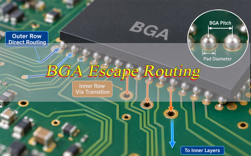
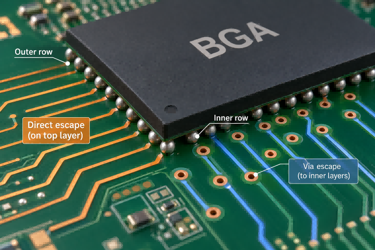
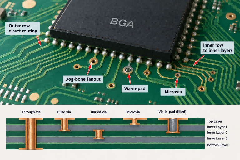
Dense BGA escape Plan layer transitions, via geometry, and return vias early
Low-voltage high-current ICs Design the PDN against a target-impedance requirement

High Speed PCB Design Guidelines

The most reliable high speed PCB design guidelines form a sequence: classify interfaces, plan placement, freeze the stackup with the fabricator, define impedance and timing constraints, route the most critical nets first, simulate where margin is uncertain, and verify the released fabrication data.

  1. Classify signal groups. Record interface standard, data rate, edge rate, target impedance, topology, timing limits, and expected channel length.
  2. Place around signal flow. Keep high-speed paths short and direct while reserving space for termination, decoupling, escape routing, and test access.
  3. Agree on a manufacturable stackup. Confirm laminate family, dielectric thickness, copper weight, layer order, finished board thickness, and impedance structures before final routing.
  4. Protect return paths. Route each critical signal over a continuous reference plane and provide a local return transition when the signal changes reference layers.
  5. Control discontinuities. Review connector launches, pads, neck-down sections, vias, stubs, test points, and plane voids as part of the channel.
  6. Verify, do not guess. Use the interface vendor’s layout guide, field-solver results, SI/PI simulation, DRC constraints, and fabrication feedback.

These high speed PCB design rules are a framework, not a substitute for the component manufacturer’s limits. A generic rule should never override a tighter PCIe, DDR, USB, Ethernet, HDMI, MIPI, SerDes, or FPGA requirement.

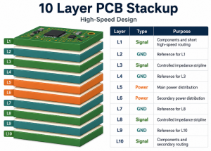
Labeled high speed PCB stackup with signal, ground, power, core, and prepreg layers

How Should the PCB Stackup Be Planned?

The stackup should be planned before detailed routing because it determines the available reference planes, impedance geometry, layer-transition behavior, dielectric loss, copper roughness exposure, and routing capacity. Changing it after routing can invalidate trace widths, differential spacing, propagation delay, and loss estimates.

Each critical signal layer should have a nearby continuous reference plane. Avoid placing two high-speed signal layers next to each other without a plane between them unless coupling has been evaluated. Power and ground planes placed close together can also improve high-frequency plane capacitance, but the PDN still needs a complete impedance analysis.

Do not select layer count from a generic chart alone. I/O density, escape routing, number of high-speed interfaces, power rails, board thickness, via structures, shielding needs, and cost all influence the construction. Before routing, ask the fabricator to confirm that the proposed dielectric thicknesses, copper weights, materials, and trace geometries are available and controllable.

Which Materials Work for High Speed PCB Design?

The right material is the lowest-cost system that still meets the channel’s loss, impedance, thermal, reliability, and fabrication requirements. Standard FR-4 can support many short, moderate-speed channels, while longer routes and higher Nyquist frequencies may require lower-loss laminates.

Material Decision Engineering Impact
Dk and its tolerance Affects impedance and propagation delay
Df at the relevant frequency Contributes to dielectric insertion loss
Copper roughness Increases conductor loss as frequency rises
Glass-weave construction Can influence differential skew in sensitive channels
Resin system and Tg Affect fabrication, thermal reliability, and lead-free processing
Material availability Changes achievable stackup, cost, and production continuity

Material data must be evaluated at the frequency and test method relevant to the design. Marketing labels such as “high speed” or “low loss” do not by themselves prove that a laminate meets the channel budget. Hybrid constructions can reduce cost, but bonding, z-axis expansion, copper treatment, drill behavior, and stackup symmetry still need fabrication review.

How Do Controlled Impedance and Return Paths Work?

Controlled impedance depends on the complete transmission-line geometry: trace width and thickness, dielectric height, Dk, nearby copper, reference-plane continuity, and differential-pair spacing. The target comes from the interface specification; the final trace geometry should come from the released stackup and an appropriate field solver.

A continuous return path is equally important. High-frequency return current concentrates near the signal route on its reference plane. If the trace crosses a split, void, anti-pad field, connector discontinuity, or poorly planned reference-layer change, the current must detour. That larger loop increases inductance, radiation, coupling, and impedance disturbance.

For a deeper manufacturing view, see our impedance control PCB guide. The fabrication drawing should state the controlled nets, target values, tolerance, reference layer, coupon requirement, and any reporting requirement rather than relying on trace width alone.

Labeled high speed PCB continuous return path and layer transition with a return via

What Are the Key Differential Pair and Length-Matching Rules?

Differential-pair routing should preserve the impedance, symmetry, return path, and timing budget defined by the interface. Pair spacing and length tolerance are not universal numbers; they depend on the stackup, coupling mode, data rate, receiver margin, and vendor specification.

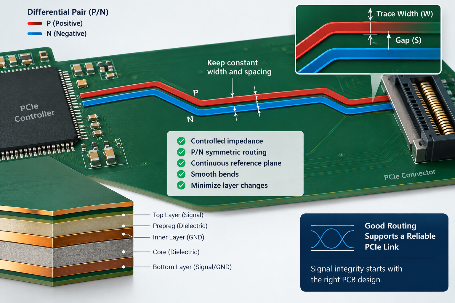
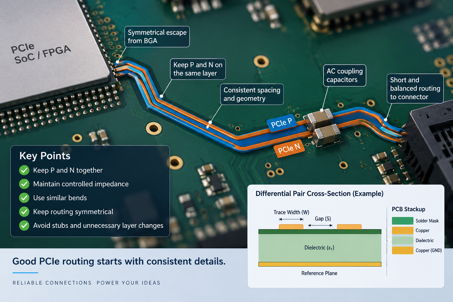
  • Route both conductors on the same layer with consistent width and spacing where possible.
  • Keep reference-plane conditions and via transitions symmetrical.
  • Limit unnecessary uncoupled sections around pads, vias, and connectors.
  • Apply intra-pair and inter-lane tuning only to the groups that require it.
  • Avoid dense serpentine tuning that creates self-coupling or moves delay into an electrically different area.
  • Check skew in time, not only in physical length, when layers or materials differ.

Our differential pair PCB guide explains impedance, routing, and length matching in more detail. For final verification, inspect the complete channel rather than judging a pair only by its visual symmetry.

How Should Vias and Layer Transitions Be Managed?

Every high-speed via transition adds an impedance discontinuity and changes the return-current path. The effect depends on barrel length, pad and anti-pad geometry, unused stub length, layer assignment, nearby return vias, and the frequency content of the signal.

Keep the number of transitions as low as the routing allows. When a signal changes layers, provide a nearby ground return via if its reference plane changes. For demanding serial channels, model the launch and review whether backdrilling, blind vias, or HDI microvias are justified. These options can improve the channel, but they also change manufacturing cost, registration requirements, and inspection needs.

Read our PCB backdrill guide before specifying stub removal. The drawing should define the drilled-from side, target layer, residual stub requirement, applicable holes, and inspection method.

Labeled comparison of a high speed PCB via stub and a backdrilled via

How Do Power Integrity and Decoupling Affect the Layout?

Power integrity affects timing margin because high-speed receivers and transmitters rely on stable supply rails and low-noise references. The PDN should remain below its target impedance across the frequency range where the voltage regulator, bulk capacitors, MLCCs, package, and plane structure supply transient current.

Place decoupling capacitors to minimize the current loop through the capacitor pads, vias, planes, and IC power pins. Select values and packages from an impedance model rather than assuming that more capacitance always solves the problem. Anti-resonance between components, via inductance, plane spreading inductance, and package effects can create unexpected peaks.

Our high-speed PCB power integrity guide covers PDN analysis and simulation. SI and PI reviews should share the same stackup because return planes, reference noise, and power-plane cavities can affect the observed eye.

Which High Speed PCB Design Software and Simulation Tools Are Useful?

High speed PCB design software should support constraint-driven routing, stackup and impedance definition, differential pairs, length and delay tuning, design-rule checking, and manufacturable output. Simulation tools are most valuable when they answer a specific risk question rather than producing plots without acceptance criteria.

Tool Function Question It Should Answer
2D field solver Which trace geometry meets the impedance target?
Pre-layout SI simulation Which topology, termination, stackup, and material provide margin?
Post-layout channel simulation Do routing, vias, connectors, and loss meet the eye or channel requirement?
PI/PDN simulation Does the supply network stay below target impedance?
EMI/EMC analysis Where do return discontinuities and resonant structures create risk?
Manufacturing DRC/DFM Can the released geometry be fabricated and inspected consistently?

Use the component vendor’s IBIS or other approved models where available, and document assumptions such as material properties, copper roughness, package models, connector models, temperature, and process tolerance. A simulation is only as credible as its model boundaries.

What DFM Data Should Be Agreed With the Fabricator?

High-speed DFM should begin before final routing, not after Gerber export. The designer and PCB manufacturer must agree on the stackup and impedance construction because a small change in dielectric thickness, copper weight, material, or etching compensation can change the electrical result.

  • Released stackup with material family, core and prepreg selection, copper weights, and finished thickness
  • Controlled-impedance table with net class, target, tolerance, layer, and reference plane
  • Critical trace, pair, spacing, delay, and skew constraints
  • Via types, backdrill details, filled-via requirements, and residual-stub limits
  • Coupon design, impedance test method, report format, and acceptance criteria
  • Material substitution rules and the approval path for any stackup change
  • Gerber or ODB++ data, drill files, netlist, fabrication drawing, and revision control

These high speed PCB design considerations also affect quotation. Low-loss laminates, tighter impedance tolerance, additional layers, HDI structures, backdrilling, extra coupons, and specialized testing may improve performance but can increase material cost, process steps, and lead time.

What Common Failures Should Be Checked Before Fabrication?

The most expensive high-speed failures are often created before fabrication data is released. A focused review should look for discontinuities and requirement gaps that a normal connectivity DRC cannot detect.

Failure Risk Pre-Fabrication Check
Reflection or poor eye opening Review impedance changes, launches, stubs, termination, and channel loss
Crosstalk Check parallel exposure, layer assignment, spacing, and reference-plane shielding
Unexpected skew Compare electrical delay through layers, vias, packages, and fiber weave
EMI failure Trace return-current paths and inspect splits, voids, connectors, and loop areas
PDN resonance Review target impedance, capacitor models, mounting inductance, planes, and package
Fabrication mismatch Freeze the approved stackup, material, impedance table, coupons, and substitution rules

Post-layout simulation and prototype measurements should target the interfaces with the least margin. Depending on the product, verification may include TDR, impedance coupons, VNA measurements, eye diagrams, jitter analysis, bit-error-rate testing, protocol compliance testing, and functional stress tests. Our eye diagram signal integrity guide explains how to interpret eye height, width, jitter, and closure.

FAQ About High Speed PCB Design

Is every high-frequency clock automatically a high-speed PCB signal?

No. The decision depends on edge time, channel delay, interconnect geometry, and required margin. A lower-frequency signal with a fast edge and long trace may need transmission-line treatment, while a physically short route with slower transitions may be less sensitive.

Can a four-layer PCB support high-speed interfaces?

It can support some interfaces when the stackup provides continuous references and sufficient routing space. The correct layer count depends on I/O density, power rails, interface count, loss targets, via strategy, and EMC requirements. Do not select four layers only because a generic example worked elsewhere.

Are 50-ohm and 100-ohm impedance values always required?

No. They are common targets, but the correct single-ended or differential impedance comes from the interface specification. Some standards use other values. The drawing and impedance table should state the exact target, tolerance, layer, reference plane, and controlled nets.

Does every high-speed PCB require a low-loss laminate?

No. Material selection depends on channel length, Nyquist frequency, insertion-loss budget, copper roughness, temperature, reliability, and cost. Shorter channels may work on suitable FR-4 systems, while longer or faster links may need lower-loss materials.

Should all differential pairs be length matched?

Match only to the tolerance required by the interface and timing budget. Unnecessary tuning can add loss, coupling, and routing congestion. The design should distinguish intra-pair skew, lane-to-lane skew, bus timing, and absolute maximum length.

What files help a PCB manufacturer review a high-speed design?

Provide Gerber or ODB++ data, drill files, netlist, fabrication drawing, released stackup, material requirements, impedance table, critical constraints, backdrill details, coupon requirements, quantity, and revision information. Share the substitution and approval rules before material procurement.

How Can EBest Circuit Support High Speed PCB Design and Manufacturing?

At EBest Circuit, we support a manufacturable high speed PCB design from stackup and DFM review through prototype fabrication, testing, repeat production, and optional PCB assembly. Our verified capabilities include high-speed PCB, high-frequency PCB, HDI, multilayer FR-4, impedance control, AOI, electrical testing, impedance testing, microsection inspection, and copper-thickness testing.

Send your Gerber or ODB++ data, stackup, impedance table, material preference, via and backdrill requirements, quantity, and test requirements to sales@bestpcbs.com. We will review the construction and identify questions that should be resolved before material release and production.
You may also like

Heavy Copper PCB Manufacturer for High Current and Power Applications

August 28th, 2026

A heavy copper PCB manufacturer builds boards for applications that require higher current capacity, improved heat dissipation, and stronger mechanical reliability than standard copper PCB constructions. By increasing copper thickness on inner or outer layers, these PCBs can support high-power circuits used in battery systems, power converters, industrial equipment, EV charging systems, renewable energy controls, and other demanding electrical applications.

EBest Circuit provides custom heavy copper PCB manufacturing with support for thick copper layers, mixed copper stack-ups, high-current designs, and complex multilayer structures. Our engineering team reviews copper thickness, layer configuration, thermal requirements, via structures, and manufacturing feasibility before production to help customers develop reliable power PCB solutions. Send your Gerber files, stack-up requirements, or application details to sales@bestpcbs.com for engineering review and quotation.

Heavy copper PCB with thick copper layers for high-current power applications

What Maximum Copper Thickness Can Be Achieved for Heavy Copper PCBs?

The maximum copper thickness of a heavy copper PCB depends on the layer position, board size, copper distribution, etching requirements, and manufacturing process capability. Unlike standard PCBs using 1 oz or 2 oz copper, heavy copper designs require specialized processing to maintain copper thickness consistency and reliable circuit formation.

EBest Circuit supports the following verified standard and special-project copper ranges. PCB copper weight must be evaluated with board size, copper distribution, spacing, dielectric fill, and process requirements.

Copper Location Typical Thickness Capability
Inner layer copper Standard 0.5–5 oz; special projects 5–20 oz
Outer layer copper Standard 1–5 oz; special projects 5–20 oz
Mixed copper designs Available after stack-up and DFM review
100 oz+ request Project-specific engineering review; not a standard capability

For 100 oz+ copper PCB designs, additional engineering evaluation is required because extremely thick copper affects:

  • Trace geometry and etching compensation
  • Copper distribution balance
  • Lamination pressure and resin filling
  • Thermal stress during manufacturing
  • Finished board weight and mechanical strength

Heavy copper capability is not only determined by copper thickness. A reliable manufacturing process must also maintain proper layer alignment, insulation spacing, and plated hole quality.

What Heavy Copper PCB Stack-Up Configurations Are Available?

Heavy copper PCBs can be manufactured with different stack-up structures depending on current requirements, thermal performance, signal requirements, and cost targets.

Typical four-layer, six-layer, mixed-copper, and thermal-via PCB stack-up configurations

Typical configurations include:

Stack-Up Type Typical Application
4-layer heavy copper PCB Power control boards, industrial electronics
6-layer mixed copper PCB Power and signal integration
Heavy copper outer layers with standard inner layers High current connection areas
Heavy copper power layers with thermal vias Heat-sensitive applications

A high current PCB stackup often combines heavy copper layers with standard signal layers. This approach allows engineers to increase current capacity in specific areas without unnecessarily increasing the cost and weight of the entire PCB.

A typical multilayer structure may include:

  • Thick copper power planes for current distribution
  • Standard copper signal layers for control circuits
  • Dedicated thermal layers for heat spreading
  • Controlled impedance layers when high-speed signals are required

The final stack-up should be reviewed during the engineering stage to ensure copper thickness, dielectric thickness, and manufacturing capability are properly matched.

Which Materials and Prepreg Systems Are Used for Heavy Copper PCBs?

Heavy copper PCB materials must provide sufficient mechanical strength, thermal stability, and reliable insulation performance under high current operation.

FR-4, high-Tg FR-4, high-resin prepreg, and thermal material systems for heavy copper PCBs

Common material options include:

Material System Application Advantage
Standard FR-4 General heavy copper applications
High Tg FR-4 Higher thermal reliability
Thermal management materials Improved heat dissipation
High resin content prepreg Better copper gap filling

Prepreg selection is especially important for heavy copper multilayer boards. Thick copper creates larger height differences between copper areas, requiring sufficient resin flow during lamination to prevent voids and ensure reliable insulation.

Material selection depends on:

  • Operating temperature
  • Current load
  • Thermal cycling requirements
  • Mechanical environment
  • Industry requirements

For high-power applications, engineers should consider both copper thickness and laminate performance rather than focusing only on copper weight.

What Surface Finish Options Are Available for Heavy Copper PCBs?

Surface finish selection depends on component requirements, assembly process, reliability expectations, and storage conditions.

ENIG, lead-free HASL, HASL, and OSP surface finish options for heavy copper PCBs

Common surface finishes for heavy copper PCBs include:

Surface Finish Typical Application
ENIG Fine-pitch components and high reliability applications
Lead-free HASL Cost-effective industrial applications
HASL Traditional soldering applications
OSP Short-term storage and standard assembly

For high-current PCBs, surface finish selection should also consider:

  • Contact reliability
  • Solder joint performance
  • Assembly temperature profile
  • Long-term environmental exposure

The correct surface finish helps maintain reliable electrical connections throughout the product lifecycle.

What Are the Design Rules and Manufacturing Tolerances for Heavy Copper PCBs?

Heavy copper PCB design requires additional attention compared with standard PCB manufacturing because thicker copper changes trace geometry, spacing requirements, and fabrication conditions.

Important design considerations include:

Design Factor Engineering Consideration
Trace width and spacing Requires copper thickness compensation
Copper distribution Avoid excessive imbalance between layers
Clearance Must consider thicker copper profiles
Impedance control Requires stack-up-based calculation
Thermal design Optimize copper planes and heat paths

During DFM review, engineers typically evaluate:

  • Copper thickness versus minimum trace width
  • Etching capability
  • Layer-to-layer registration
  • Resin filling conditions
  • Finished board thickness

These high current PCB design guidelines should be confirmed against the proposed copper weight and stack-up during an engineering DFM review. Early communication helps avoid unnecessary redesign during manufacturing.

Which Via Technologies Are Available for Heavy Copper PCB Manufacturing?

Via structures play an important role in heavy copper PCB performance because they influence current flow, thermal transfer, and mechanical reliability.

Available via technologies include:

  • Through-hole vias
  • Plated through vias
  • Thermal via arrays
  • Large diameter vias
  • Multiple parallel vias for current distribution

For power applications, engineers often use multiple thermal vias under heat-generating components or create parallel via paths to reduce electrical resistance.

Via design should consider:

  • Current requirements
  • Component heat generation
  • Copper thickness
  • Assembly conditions

A proper via structure improves both electrical performance and thermal management.

Which Standards and Certifications Apply to Heavy Copper PCBs?

Heavy copper PCB manufacturing for industrial, automotive, medical, and aerospace applications often requires compliance with recognized quality standards.

EBest Circuit supports manufacturing processes aligned with:

Standard / Certification Application
IPC-6012 Qualification and performance specification for rigid PCBs
IPC-A-600 PCB acceptance criteria
ISO 9001 Quality management system
ISO 13485 Medical device applications
IATF 16949 Automotive applications
AS9100D Aerospace applications

Specific requirements depend on the final application, customer specifications, and industry regulations.

Quality control processes may include:

  • Electrical testing
  • AOI inspection
  • X-ray inspection when required
  • Dimensional inspection
  • Copper thickness verification

What Is the Typical Lead Time for Heavy Copper PCB Production?

Heavy copper PCB lead time depends on copper thickness, layer count, board complexity, testing requirements, and production volume. Review our PCB lead-time guidance as a planning reference; the quotation confirms the actual schedule.

Typical production stages include:

Production Stage Time Consideration
Engineering review Based on design complexity
Prototype production Depends on copper thickness and stack-up
Volume production Based on quantity and process requirements

Compared with standard PCB production, heavy copper boards may require additional process controls, including:

  • Special lamination conditions
  • Copper thickness verification
  • Additional inspection steps
  • Manufacturing feasibility review

Providing complete design information during quotation helps shorten engineering evaluation time.

Recommended information includes:

  • Gerber files
  • Layer stack-up
  • Copper thickness requirements
  • Current load requirements
  • Application environment

What Design Guidelines Should Be Followed for 100 oz+ Heavy Copper PCBs?

100 oz+ heavy copper PCB requests require project-specific feasibility review because extremely thick copper affects electrical performance, manufacturing processes, and mechanical characteristics. This section provides design inputs for evaluation and does not state an unconditional production capability.

Design guidelines for 100 oz and thicker heavy copper PCBs

Key design guidelines include:

Optimize copper distribution

Large differences in copper area between layers can create lamination challenges and affect board flatness. Balanced copper distribution improves manufacturing stability.

Consider current path design

High-current paths should use:

  • Wider copper areas
  • Shorter current routes
  • Multiple copper layers when required
  • Optimized connection points

Plan thermal management early

High-power applications should consider:

  • Large copper planes
  • Thermal vias
  • Heat spreading structures
  • Component placement strategy

Complete DFM review before production

For 100 oz+ designs, customers should provide:

  • Maximum current requirement
  • Operating temperature
  • Mechanical dimensions
  • Layer stack-up preference
  • Reliability requirements

Early engineering review helps confirm whether the design is suitable for production.

Why Choose EBest Circuit for Heavy Copper PCB Manufacturing?

Selecting a heavy copper PCB supplier requires more than checking the maximum copper thickness. Manufacturing experience, engineering support, and process control directly affect final PCB reliability.

EBest Circuit provides:

  • Heavy copper PCB manufacturing capability
  • Custom multilayer PCB solutions
  • Mixed copper stack-up support
  • Engineering DFM review
  • Prototype and production support
  • PCB assembly integration capability

With more than 20 years of PCB manufacturing experience, EBest Circuit supports customers from initial design evaluation through PCB production and PCBA assembly.

For heavy copper PCB projects, contact sales@bestpcbs.com with your Gerber files, copper requirements, or application details.

Frequently Asked Questions About Heavy Copper PCBs

What copper thickness is considered a heavy copper PCB?

Heavy copper PCBs generally refer to boards using copper thickness above standard PCB levels, commonly starting from 3 oz copper and extending to much higher copper weights depending on the application.

Can you manufacture 100 oz copper PCB?

100 oz+ copper PCB requests require project-specific engineering review. Feasibility can be confirmed only after board size, layer structure, copper distribution, insulation, drilling, plating, and reliability requirements are evaluated.

What applications use heavy copper PCBs?

Heavy copper PCBs are commonly used in power supplies, battery systems, EV equipment, industrial controls, renewable energy systems, and high-current electronics.

What materials are recommended for heavy copper PCBs?

High Tg FR-4, suitable prepreg systems, and thermal management materials are commonly selected based on operating temperature and reliability requirements.

Can heavy copper PCBs include controlled impedance designs?

Yes. Controlled impedance can be considered when heavy copper layers are combined with appropriate dielectric thickness and stack-up planning.

What files are needed for heavy copper PCB quotation?

Customers should provide Gerber files, layer stack-up information, copper thickness requirements, board dimensions, quantity, and application details.

Request a Heavy Copper PCB Manufacturing Review

Whether you need a standard heavy copper PCB or want feasibility feedback on a 100 oz+ high-current concept, EBest Circuit can review your design requirements and provide manufacturing recommendations.

Send your PCB files or technical requirements to sales@bestpcbs.com for engineering evaluation and quotation.

You may also like

High Voltage PCB Design Guidelines for Safe and Reliable Boards

August 28th, 2026

A high voltage PCB has to do more than carry a higher electrical potential. Its layout, insulation system, laminate, conductor geometry, surface condition, and manufacturing tolerances all influence whether the finished board can operate safely without arcing, surface tracking, insulation breakdown, or premature field failure.

EBest Circuit supports high-voltage PCB fabrication and PCBA projects from prototype through production. For projects involving special insulation spacing, heavy copper, controlled dielectric thickness, isolation slots, or unusual stack-ups, send your Gerber files, stack-up, operating voltage, peak voltage, material requirements, and application information to sales@bestpcbs.com for an engineering review and quotation.

High voltage PCB design guidelines showing creepage, clearance, insulation, and multilayer isolation

What Is a High Voltage PCB?

A high voltage PCB is a circuit board designed with additional insulation, spacing, material, and layout controls to safely handle elevated voltage differences between conductors.

There is no single PCB-industry voltage threshold above which every circuit automatically becomes a high-voltage PCB. In practical power-electronics work, approximately 300 V to 1,000 V is a useful range where high-voltage spacing and insulation considerations become increasingly important, while properly engineered boards can operate above 1 kV.

Typical applications include:

  • EV charging and battery systems
  • Industrial power supplies
  • Solar inverters
  • Motor drives
  • High-voltage test equipment
  • Medical electronics
  • Power conversion equipment
  • Energy storage systems
  • High-voltage measurement circuits

The key distinction is therefore not simply the number printed beside the voltage rail. A reliable design has to manage insulation coordination across traces, pads, layers, component leads, PCB edges, slots, coatings, and the surrounding environment.

How Much Voltage Can a PCB Handle?

For practical high-voltage PCB design, working voltages around 300–1,000 V are common design territory, while specially engineered PCBs can operate above 1 kV; there is no universal maximum PCB voltage rating.

The actual limit is usually determined by the weakest insulation path rather than by the FR-4 laminate alone.

For example, a laminate may have high dielectric strength while an assembled PCB still fails because two exposed pads are too close, contamination forms a conductive surface path, or an unexpected surge exceeds the designed clearance.

Voltage capability is influenced by:

  • Working voltage: continuous or repetitive voltage between conductors
  • Peak voltage: maximum DC or AC peak potential difference
  • Transient voltage: switching spikes and surge events
  • Clearance: shortest air path between conductive parts
  • Creepage: shortest surface path between conductive parts
  • Dielectric thickness: insulation between PCB layers
  • Material CTI: resistance to surface tracking
  • Altitude: lower air pressure reduces air insulation capability
  • Pollution and moisture: contamination can reduce surface resistance

For design and RFQ purposes, it is therefore more useful to specify working voltage + peak/transient voltage than to state only “1,000 V PCB.”

What Is the Difference Between Creepage and Clearance in High Voltage PCB Design?

Clearance is the shortest distance through air between two conductive parts, while creepage is the shortest distance along an insulating surface.

Parameter What It Measures Main Failure Risk
Clearance Shortest path through air Arcing / air breakdown
Creepage Shortest path along an insulating surface Surface tracking
Solid insulation Path through dielectric material Dielectric breakdown
Creepage versus clearance on a high voltage PCB with isolation slot and cross-section

Suppose two high-voltage pads are separated by a routed slot. The slot can substantially lengthen the surface path and therefore increase creepage, but the shortest air path must still be checked separately for clearance.

This distinction matters because the two distances are determined differently. Clearance is strongly influenced by transient voltage and altitude, while creepage depends heavily on working voltage, pollution degree, and the CTI of the insulating material.

How Do You Determine High Voltage PCB Clearance and Creepage?

As a practical example, at 400 V RMS, IEC 60664-1 gives a creepage reference of about 2.0 mm for Pollution Degree 2 and Material Group I, but the requirement increases to about 4.0 mm for Material Group III.

That difference is why voltage alone cannot determine the final spacing.

Typical IEC 60664-1 creepage references for Pollution Degree 2 are:

Working Voltage Material Group I Material Group II Material Group III
400 V RMS 2.0 mm 2.8 mm 4.0 mm
800 V RMS 4.0 mm 5.6 mm 8.0 mm
1,000 V RMS 5.0 mm 7.1 mm 10.0 mm

These values illustrate how strongly material tracking performance can affect creepage.

The design sequence should be:

  1. Determine the actual working voltage.
  2. Identify the maximum transient or impulse voltage.
  3. Define whether the insulation is functional, basic, supplementary, or reinforced.
  4. Determine the pollution degree.
  5. Check the laminate CTI and material group.
  6. Account for operating altitude.
  7. Apply the requirements of the relevant end-product standard.

Clearance follows a different calculation path.

For example, typical IEC 60664-1 basic-insulation clearance values at up to approximately 2,000 m include:

Required Impulse Voltage Typical Minimum Clearance
0.5 kV 0.2 mm
1.5 kV 0.5 mm
2.5 kV 1.5 mm
4.0 kV 3.0 mm
6.0 kV 5.5 mm

This demonstrates why a 400 V circuit cannot automatically be assigned “a 400 V clearance.” Its required clearance may instead be controlled by a 2.5 kV, 4 kV, or higher impulse requirement.

What High Voltage PCB Trace Spacing Should You Use?

For external uncoated conductors, a useful PCB design reference is approximately 1.25 mm at 151–300 V peak and 2.5 mm at 301–500 V peak; at 1,000 V, the spacing reaches about 5.0 mm under the familiar IPC external-uncoated conductor rule.

A practical reference table is:

Voltage Difference, DC or AC Peak External Uncoated Conductor Spacing
31–150 V 0.60 mm
151–300 V 1.25 mm
301–500 V 2.50 mm
600 V ≈3.0 mm
800 V ≈4.0 mm
1,000 V ≈5.0 mm
High voltage PCB trace spacing infographic with voltage-to-spacing guide

For values above 500 V, the external-uncoated reference increases by approximately 0.005 mm per volt above 500 V.

For example:

1,000 V: 2.5 mm + (500 × 0.005 mm) = 5.0 mm

IPC-2221C is the current IPC-2221 revision. It retains conductor-spacing categories while refining areas such as altitude, vacuum operation, and coating definitions, so the current standard should be checked when establishing released design rules.

These PCB conductor-spacing values should not be treated as the final safety clearance for every product. Medical, mains-powered, industrial, automotive, or reinforced-insulation designs may require greater spacing under their applicable IEC or UL safety standard.

Designers should also check more than trace-to-trace spacing:

  • trace to pad
  • pad to pad
  • copper to board edge
  • trace to mounting hole
  • trace to chassis
  • copper to exposed component lead
  • high-voltage to low-voltage plane
  • outer-layer to inner-layer conductor

The correct design value is the minimum finished-board distance after manufacturing tolerance, not merely the nominal CAD spacing.

Which Materials Are Best for a High Voltage PCB?

High-CTI FR-4 is suitable for many high-voltage PCBs, while specialized high-voltage laminates become more attractive when surface tracking, humidity, thermal stress, or insulation reliability is more demanding.

The most important properties include:

Material Property Why It Matters
CTI Resistance to conductive surface tracking
Dielectric strength Resistance to breakdown through insulation
Moisture resistance Helps preserve insulation in humid environments
CAF resistance Reduces conductive filament reliability risk
Tg Influences thermal dimensional stability
Td Indicates thermal decomposition behavior
Resin system Affects insulation and processing behavior
Z-axis stability Important for multilayer reliability

CTI is not the same as dielectric strength.

Dielectric strength concerns breakdown through the insulating material.

CTI evaluates resistance to conductive tracking across its surface.

This is why two FR-4 materials with similar dielectric strength can require different creepage distances when their CTI classifications differ.

For demanding designs, specifying only “FR-4” is therefore insufficient. The RFQ should identify either the laminate grade or the required CTI, thermal, flammability, and insulation properties.

How Should You Plan the Stack-Up for a High Voltage PCB?

A high-voltage stack-up should first separate HV and low-voltage domains with controlled dielectric thickness, rather than simply adding layers around an existing layout.

The exact dielectric thickness cannot be reduced to one universal number because it depends on the required solid-insulation voltage withstand, laminate system, insulation class, and applicable product standard.

The stack-up should define:

  • dielectric thickness between high-voltage layers
  • high-voltage-to-low-voltage layer separation
  • copper thickness
  • material dielectric properties
  • resin content
  • finished board thickness
  • internal plane clearances
  • via structures crossing voltage domains

Internal copper is surrounded by solid dielectric, so its insulation mechanism differs from exposed surface copper.

Avoid placing a low-voltage or grounded plane immediately underneath a high-voltage node unless the vertical insulation path has been intentionally evaluated.

High-current high-voltage designs need another check. Increasing copper weight can reduce conductor resistance, but heavier copper also changes etching capability, conductor spacing, resin fill, dielectric construction, and finished board thickness.

For unusual HV constructions, stack-up review should therefore happen before final routing, not after the Gerber files are complete.

What Are the Key High Voltage PCB Layout Guidelines?

The most effective layout rule is to create clearly separated HV and LV zones and maintain the required isolation distance around the complete boundary on every copper layer.

Useful layout practices include:

  • Separate HV and SELV/low-voltage areas.
  • Maintain the isolation boundary on every copper layer.
  • Avoid sharp copper points in high-electric-field regions.
  • Use smooth trace and copper transitions where practical.
  • Keep HV copper away from uncontrolled PCB edges.
  • Include vias and plated holes when checking spacing.
  • Avoid unnecessary test points inside HV areas.
  • Keep contamination-sensitive regions accessible for cleaning.
  • Check component body and lead spacing.
  • Prevent copper pours from entering isolation gaps.

A common design error is creating a large visible clearance on the top layer while an internal copper plane extends underneath the same isolation barrier.

Another occurs around components. The traces may meet the intended rule while transformer pins, connector contacts, heat sinks, screws, or component leads create a shorter path.

A high-voltage layout review should therefore inspect the finished electrical assembly, not only individual traces.

When Should You Use Isolation Slots, Barriers, or Conformal Coating?

Use an isolation slot when PCB area is limited and additional creepage is needed; use barriers when the physical insulation path needs to be extended; use conformal coating mainly when environmental contamination or moisture must be controlled.

High voltage PCB layout protection methods using isolation slots, barriers, and conformal coating

These three methods solve different problems.

Isolation slots interrupt the direct PCB surface path and can significantly increase creepage without requiring the same increase in board width.

Barriers physically extend or separate insulation paths and may also help prevent contamination from bridging conductive regions.

Conformal coating protects the PCB from humidity, dust, chemicals, and surface contamination.

Coating performance depends on:

  • coating material
  • thickness
  • adhesion
  • coverage
  • cure quality
  • pinholes
  • component shadowing
  • operating environment
  • applicable standard

Do not assume that ordinary solder mask or conformal coating automatically allows a safety clearance to be reduced.

If an isolation slot is safety-critical, specify its finished minimum width, position, and tolerance on the manufacturing documentation rather than relying only on nominal CAD geometry.

Which Standards Apply to High Voltage PCB Design?

For general PCB design, IPC-2221C is a key reference; for insulation coordination, IEC 60664-1 is one of the most important standards, while the final equipment standard determines the binding safety requirement.

Standard Typical Relevance
IPC-2221C Generic printed board design and conductor spacing
IEC 60664-1 Clearance, creepage, insulation coordination
IEC 62368-1 AV and ICT equipment
IEC 60601-1 Medical electrical equipment
UL 796 Printed wiring boards
Product-specific IEC/UL standards Final equipment safety requirements

The key point is that an IPC spacing table does not automatically prove product safety compliance.

A medical device, EV charger, industrial controller, mains power supply, or ICT product may require different insulation levels even if their PCB operating voltages appear similar.

What Manufacturing Factors Matter for High Voltage PCBs?

The most critical manufacturing requirement is that the finished PCB must preserve the minimum insulation distances assumed by the designer after etching, drilling, routing, lamination, and registration tolerances are included.

Key controls include:

  • Copper geometry: etching must not reduce critical spacing.
  • Copper-to-edge distance: routing tolerance must be included.
  • Isolation slots: finished dimensions must meet the required minimum.
  • Dielectric thickness: critical insulation layers must match the approved stack-up.
  • Material control: laminate substitutions require engineering review.
  • Surface cleanliness: ionic contamination can weaken surface insulation.
  • Solder mask registration: misalignment may expose copper.
  • Routing and drilling accuracy: holes and slots can alter creepage paths.
  • Lamination quality: voids and delamination are undesirable in stressed dielectric structures.
  • Traceability: safety-related products may require controlled material and process records.

For example, if a design requires a 2.50 mm finished minimum conductor spacing, drawing two features exactly 2.50 mm apart in CAD leaves no manufacturing tolerance.

This is why high-voltage fabrication notes should clearly distinguish between the nominal design dimension and the minimum finished-board requirement. That distinction helps ensure normal fabrication tolerances do not reduce critical spacing below the required minimum.

High voltage PCB manufacturing controls and electrical verification including hipot and insulation resistance testing

How Should a High Voltage PCB Be Tested?

At minimum, a high-voltage PCB should receive normal open/short electrical testing; projects with safety-related insulation commonly add insulation-resistance and dielectric-withstand, or hipot, testing according to the product specification.

Depending on the application, verification may include:

  • open/short electrical test
  • insulation resistance test
  • dielectric withstand / hipot test
  • dimensional inspection of isolation gaps
  • isolation-slot inspection
  • cleanliness testing
  • conformal-coating inspection
  • functional testing at operating voltage
  • first-article validation

A hipot test applies a specified voltage between isolated regions and checks whether the insulation can withstand that electrical stress without unacceptable leakage or breakdown.

There is no responsible universal rule such as:

“Test every 1,000 V PCB at 2,000 V.”

The correct hipot voltage and duration come from the end-product standard or approved test specification.

The test document should define:

  • test voltage
  • AC or DC
  • duration
  • ramp rate
  • leakage-current limit
  • test points
  • pass/fail criteria

For assembled boards, PCB-only testing may not be enough. Connectors, component leads, heat sinks, screws, cables, and other hardware can create shorter insulation paths than the bare board itself.

What High Voltage PCB Design Mistakes Should You Avoid?

The most common high-voltage PCB mistake is choosing spacing from nominal operating voltage alone instead of evaluating peak voltage, creepage, clearance, environment, and manufacturing tolerance together.

Other common problems include:

  • Confusing clearance with creepage. Increasing the surface path does not automatically increase the air path.
  • Ignoring altitude. Above approximately 2,000 m, IEC insulation calculations may require clearance correction.
  • Selecting laminate only by dielectric strength. CTI, moisture resistance, thermal behavior, and contamination also matter.
  • Assuming solder mask provides reinforced insulation. This depends on the construction and applicable safety standard.
  • Ignoring internal copper. An outer-layer isolation zone can still contain a hidden plane violation.
  • Leaving sharp copper features in HV regions. Sharp geometry can increase local electric-field concentration.
  • Checking PCB traces but not components. Leads, terminals, heat sinks, connectors, and hardware must also maintain isolation.
  • Designing exactly to the minimum spacing. Fabrication tolerances must be added before design release.

A useful high-voltage design review question is therefore:

Does the finished and assembled product maintain the required insulation under its actual voltage, transient, altitude, contamination, manufacturing tolerance, and service conditions?

FAQs About High Voltage PCB

What voltage is considered high voltage on a PCB?

There is no universal PCB threshold, but approximately 300 V and above is a useful practical point at which clearance, creepage, transients, insulation, and environmental conditions deserve explicit review. Designs in the 300–1,000 V range are common high-voltage PCB territory, while boards above 1 kV are feasible with appropriate engineering.

How much clearance does a high voltage PCB need?

For external uncoated PCB conductors, a useful IPC reference is about 1.25 mm for 151–300 V peak and 2.50 mm for 301–500 V peak, increasing to approximately 5.0 mm at 1,000 V under the external-conductor rule. Product-safety requirements can require larger values.

What is the difference between creepage and clearance?

Clearance is the shortest path through air, while creepage is the shortest path along an insulating surface.

Is FR-4 suitable for high voltage PCBs?

Yes. High-CTI FR-4 is suitable for many 300–1,000 V-class PCB applications, provided its CTI, dielectric construction, thermal performance, creepage, clearance, and end-product requirements are appropriate.

Does conformal coating increase voltage isolation?

It can improve environmental protection and surface insulation performance, but it does not automatically justify smaller safety spacing. The coating material, coverage, process qualification, and applicable standard must support the reduction.

How does altitude affect PCB clearance?

Clearance normally increases with altitude because air density decreases. Above approximately 2,000 m, the applicable standard may require an altitude correction factor.

Can isolation slots increase creepage distance?

Yes. A correctly placed slot can substantially increase creepage without requiring the same increase in PCB width, although clearance must still be checked separately.

If you are developing a high-voltage PCB and want the fabrication capability checked before prototype release, send your Gerber files, stack-up, working voltage, peak or surge voltage, copper weight, material requirements, critical isolation dimensions, and applicable standard to sales@bestpcbs.com. EBest Circuit can review stack-up manufacturability, critical spacing, isolation slots, copper geometry, dielectric construction, and other fabrication-sensitive features before quotation and production.
You may also like

Car Charger Circuit Board Manufacturing and Assembly for USB-A, USB-C and USB PD Modules

August 27th, 2026

A car charger circuit board converts vehicle power into a stable USB output while protecting the connected device and managing charging behavior. The car charger circuit board combines an input protection stage, a DC-DC power stage, a charging or USB controller, filtering and the output connector in a compact space. This article covers low-voltage automotive USB charging modules used in plug-in, dashboard and center-console products, not EV traction-battery or onboard chargers.

The practical challenge is not simply making the USB port turn on. An automotive USB charger PCB must carry the required current without excessive voltage drop, remove heat from the switching components, survive the specified electrical environment and keep the connector mechanically stable. If your design files are ready, send the Gerber or ODB++, BOM, schematic, mechanical data and test requirements to sales@bestpcbs.com for a free DFM review.

Car charger circuit board, manufacturing and assembly for an automotive USB charging module

What Is a Car Charger Circuit Board and How Does It Work?

A car charger PCB is a compact power-conversion assembly that turns the vehicle supply into the voltage and charging behavior required at one or more USB ports. Power normally enters through the module connector, passes through protection and filtering, reaches the switching converter, and then flows through the charging controller or port controller to the USB output.

  • Input protection: Limits damage from reverse connection, overvoltage, transient events or a short that the product specification requires the module to withstand.
  • DC-DC conversion: Regulates the varying vehicle input to the output needed by the selected charging architecture.
  • Charging control: Identifies or negotiates the permitted output behavior for USB-A, USB-C or USB Power Delivery.
  • Filtering and grounding: Contain switching noise and give the power and control circuits a stable reference.
  • Connector and enclosure path: Carry current to the cable, support insertion forces and help move heat away from the board.

These blocks work as one system. A capable controller cannot compensate for an undersized current path, and a large copper area will not solve a poor thermal connection beneath the power package. The design should therefore be reviewed from the vehicle input to the USB contact rather than as isolated components.

What Types of Car Charger PCBs Are Used for USB-A, USB-C and USB PD Modules?

The port type sets only part of the design; output behavior, available power, port count and mechanical format determine the actual circuit and assembly. Common USB car charger PCB variants include USB-A, USB-C, USB PD and multi-port boards. Two products can use the same connector while requiring different controllers, power stages, firmware and validation.

  • USB-A charging boards: Commonly combine a regulated power stage with a charging-port controller and a mechanically supported receptacle. The layout must protect output voltage from cable and connector losses, while the assembly drawing defines connector position, shell tabs and orientation.
  • USB-C charging boards: Add configuration and attachment-detection requirements. The smaller connector geometry and inaccessible joints may also change stencil design, inspection access and the method used to verify connector alignment.
  • USB PD charging boards: Require a compatible power stage, PD controller and approved configuration for the profiles the product is intended to provide. USB-IF maintains the current USB Power Delivery specification; hardware, controller configuration and functional testing should refer to the same approved product requirement.
  • Multi-port charging boards: Add power sharing, simultaneous-load behavior, denser connector placement and concentrated heat. Evaluate a dual-port board under the intended combined load rather than testing each port separately and assuming the same result.

What Electrical and Protection Requirements Affect a Car Charger Circuit Board?

The protection circuit must be selected from the customer’s defined input conditions and failure tests, not from a generic “automotive” label. Vehicle supply conditions vary by product and system. The RFQ should state the normal input range, abnormal-input conditions, transient requirements and recovery behavior that the finished module must meet.

  • Reverse-polarity protection: Confirm how the circuit blocks or tolerates an incorrect supply connection and whether the selected device creates a significant voltage or thermal penalty.
  • Overvoltage and transient protection: Coordinate the suppressor, switch and converter ratings so the first protection device does not merely pass excessive stress to the next part.
  • Overcurrent and short-circuit behavior: Define the trip, limiting and recovery response at both the input and the USB output where applicable.
  • Input and output filtering: Place the filter around the actual noisy current path and verify it with the target wiring, load and enclosure conditions.
  • Connector-side protection: Review ESD and unintended voltage exposure at the user-accessible port as part of the product requirement.

The protection parts also influence placement and heat. For example, putting a suppressor close to the input connector can shorten its discharge path, but the surrounding copper, clearances and nearby heat-sensitive components still need to suit the specified stress. The right outcome is a coordinated protection path, not the maximum part rating in every position.

Car charger circuit board, input protection and power conversion section

How Should the Power Layout Be Designed for a Car Charger PCB?

A reliable layout keeps the high-current path wide and continuous while making the switching loop physically small. The two goals are related but not identical. Current capacity depends on the complete conductor path; switching behavior depends heavily on loop area, component placement and the return path.

  • Follow the power path: Review the route from input connector to protection device, converter, inductor, output capacitor and USB connector. Pad exits, thermal reliefs, via transitions and connector contacts can be more restrictive than the main trace.
  • Minimize the switching loop: Place the switching device, inductor and high-frequency capacitors according to the controller manufacturer’s layout guidance. Keep sensitive feedback and configuration signals away from noisy nodes.
  • Provide a deliberate return path: Avoid splitting the reference beneath critical control or high-frequency paths. Ground vias should support the intended current and thermal flow rather than being added without a clear function.
  • Avoid copper neck-downs: Check changes in width at pads, fuses, shunts, vias and connector pins. Local loss and heat often appear where the conductor becomes narrow for only a short distance.
  • Plan test access: Add stable measurement points for the input, regulated output, port output and key control nodes without disturbing the power loop.

During DFM, the layout should be checked against the finished copper, drill and assembly constraints that will actually be produced. A visually broad polygon is not proof of current capacity if its connection to a pad passes through a narrow spoke or an insufficient via group.

How Should Heat Be Managed in a Compact Car Charger PCB?

Thermal control starts by identifying where loss occurs and where that heat can leave the assembled module. The converter, MOSFETs, inductor, protection devices and connector contacts can all become limiting points. Their temperatures depend on conversion loss, conductor resistance, airflow, enclosure contact and how nearby heat sources interact.

  • Copper spreading: Connect useful copper to the thermal pad or power node without enlarging the noisy switching node unnecessarily.
  • Thermal vias: Move heat into useful copper on other layers; confirm drill size, finished hole condition and solder-control strategy with the manufacturer.
  • Stencil apertures: Segment exposed-pad openings when needed to balance solder coverage, voiding risk and package seating.
  • Component spacing: Keep electrolytic capacitors, plastics and other temperature-sensitive parts away from concentrated heat where the enclosure permits.
  • Loaded measurement: Test the assembled module at defined loads and ambient conditions, then record the hottest component and voltage drop along the main power path.

A bench result with the bare board exposed may not represent a closed dashboard or console enclosure. If the product depends on a housing contact or metal heat path, that interface belongs in the validation setup and the mechanical drawing.

Car charger circuit board, thermal and electrical verification in a compact module

What PCB Materials, Copper Weight and Stackup Are Suitable for Car Charger PCBs?

FR-4 is a common starting material, but layer count, finished copper and board thickness should follow the electrical, thermal and mechanical needs of the specific module. There is no single construction that fits every car charger circuit board.

  • When two layers may fit: A two-layer board can be practical when the power is moderate, component density is low, the ground return remains continuous and enough copper area is available for current and heat spreading. Verify voltage drop, hot spots and switching behavior on the assembled module.
  • When four layers may help: Four layers become useful when the board needs a more continuous reference plane, denser routing, better separation of power and control paths, additional heat spreading or a smaller outline. Adding layers without assigning a function to them increases cost without guaranteeing better performance.
  • What the drawing should control: State the laminate or approved material requirement, final thickness, layer count, finished copper, surface finish and stackup. Copper weight alone is not a current guarantee because a narrow pad exit, via transition, solder joint or connector contact can still create local resistance and heat.
  • How to confirm the choice: Select the surface finish for the actual component, solderability, storage and customer requirements, then use fabricated-board and assembled-product results to verify that the selected construction meets the electrical, thermal and mechanical limits.

What DFM Checks Matter Before Car Charger PCB Manufacturing?

DFM should inspect the complete input-to-output path and its mechanical interfaces because current, thermal and connector failures often develop across more than one footprint. A useful review marks the exact feature, explains the possible failure and proposes a change that the customer can approve.

  • Current-path continuity: Trace the input connector to the protection stage, regulator, inductor, output capacitor and USB connector. Check every neck-down, via group, thermal relief and high-current pad.
  • Thermal-pad manufacturability: Review pad dimensions, via layout, solder-mask openings and stencil segmentation for power packages with exposed pads.
  • Connector fit: Compare the footprint, shell tabs, centerline, board edge and enclosure opening. Confirm that placement and inspection remain possible after panelization.
  • Assembly clearance: Check component spacing around the inductor, power devices and connectors for placement, soldering, rework and mechanical load.
  • Inspection and test access: Identify hidden joints and decide whether visual inspection, AOI, X-ray, a mechanical gauge or a powered test can detect the relevant defect.
  • File consistency: Cross-check Gerber or ODB++, drill data, BOM, centroid file, assembly drawing and mechanical model for revision, footprint and coordinate conflicts.

A focused car charger circuit board DFM review should distinguish a required correction from an optional cost or process suggestion. That distinction helps the buyer approve changes without turning every manufacturing preference into a product requirement.

How Is a Car Charger Circuit Board Manufactured and Assembled?

Manufacturing begins with the approved PCB construction and ends with an assembled, identified unit that can be tested against the intended charging behavior. The process route changes with the board design and component set, but the sequence should preserve product identity at every stage.

  • CAM and panel review: Confirm the approved stackup, copper features, drill data, solder mask, finish and panel method before tooling. This check catches file or clearance conflicts that could create a fabrication defect before production records are issued.
  • PCB fabrication: Build the layers, plated holes, solder mask and surface finish to the fabrication drawing. Bare-board electrical testing verifies the finished PCB for opens and shorts before assembly begins.
  • Solder-paste printing: Set stencil apertures from the approved component and footprint data. Inspect the print where fine-pitch controllers, exposed thermal pads or large power pads create bridging, insufficient-paste or voiding risks.
  • SMT placement: Place the power IC, MOSFETs, controller, inductor, capacitors and protection devices from the approved BOM with the correct orientation. Placement inspection catches a wrong, missing or shifted part before it creates a placement defect at reflow.
  • Reflow soldering: Use a profile suited to the approved solder paste, board mass and package set. Review joint formation and exposed-pad behavior because poor wetting, voiding or package lift can create electrical and thermal failures.
  • Connector and through-hole assembly: Install USB receptacles, input terminals and mechanically loaded parts according to the assembly drawing. Verify orientation, shell seating and solder joints to prevent a mechanical defect, retention failure or intermittent contact.
  • Inspection, programming and functional test: Apply the methods required by package and product failure risks, then record results against the correct PCB, BOM and program identity. Failed or mismatched units remain separated until reviewed and dispositioned.

The manufacturing record should make substitutions, rework and program changes visible. This is especially important when several variants share the same bare PCB but use different components or charging configurations.

How Are USB-C, USB PD and Power Components Controlled During Assembly?

Assembly control must prevent visually similar parts or boards from leaving production with the wrong charging function. The BOM, placement data, program file and test profile should use a shared variant identifier.

  • PD controller and configuration: Map each hardware revision to its approved configuration or firmware. Verify the loaded identity where programming is part of the build.
  • Power IC and MOSFETs: Check the exact manufacturer part number, package, orientation and thermal-pad condition. Approved alternatives require an electrical and thermal review, not just footprint compatibility.
  • Inductor and capacitors: Control electrical rating, package height, polarity where applicable and supplier-approved substitutions that can affect loss, heat or fit.
  • USB connector: Confirm connector orientation, shell seating, mechanical tabs and solder joints. Hidden joints need an inspection method suited to their geometry.
  • BOM revision: Keep consigned, turnkey and customer-approved components clearly separated so purchasing does not introduce an unreviewed alternative.

When one bare board supports several port or power variants, physical labeling and electronic identity should agree. Functional testing should then check the output behavior assigned to that variant rather than applying one generic test to every assembly.

How Should Car Charger PCBAs Be Inspected and Functionally Tested?

Inspection and testing should be selected by failure mode and production stage. No single method proves solder quality, firmware identity, charging negotiation, output stability and thermal performance.

  • Before assembly: Bare-board electrical testing checks PCB opens and shorts.
  • During assembly: SPI may be used when paste volume or alignment is a significant process risk. AOI or visual inspection can detect applicable placement, polarity and visible-joint defects.
  • For hidden joints: X-ray may be applied to selected bottom-terminated packages, exposed pads or inaccessible connector joints when it can reveal the defined defect.
  • After programming: A readback or identity check confirms the expected controller configuration where the product requires it.
  • Powered testing: No-load and loaded output, port detection, requested PD profiles and simultaneous-load behavior can be checked against customer-defined limits.
  • Product validation: Temperature rise, transient response and EMI/EMC testing belong in the plan only when the applicable specification, setup and acceptance criteria are defined.

IPC J-STD-001J and IPC-A-610J address soldering process requirements and post-assembly acceptance, respectively. Purchase documents still need to name the applicable revision, class and customer-specific criteria. Functional testing complements those checks; it does not replace structural inspection.

Car charger circuit board, functional testing of an assembled PCBA before shipment

What Common Car Charger PCB Failures Should Be Checked Before Mass Production?

Failure analysis should begin with the symptom and a reproducible operating condition because the same visible fault can come from the PCB, component, program, connector or test setup. Replacing a component or adding copper before locating the cause can hide the original defect and create a new one.

  • Excessive temperature: Measure the converter, MOSFET, inductor, protection stage and connector under the intended load. Check whether loss comes from the component, copper path, solder joint or enclosure interface.
  • Voltage drop: Measure before and after pad exits, vias, protection devices and connector contacts. The weakest short segment can dominate the total loss.
  • Unstable charging or resets: Review input transients, loop layout, grounding, output capacitance, controller configuration and the test cable or load.
  • USB recognition failure: Compare the installed controller, configuration resistors, firmware or PD profile with the intended variant.
  • Connector solder cracking: Inspect shell tabs, mechanical support, board-edge position and enclosure loading rather than treating the joint as an electrical connection only.
  • Weak multi-port performance: Test simultaneous load, power sharing and thermal concentration with both ports active.
  • EMI-related instability: Review the high-frequency loop, filter placement, reference path and cable setup before changing the entire stackup.

A corrective action is ready for the next build only after the cause, affected units, design or process change and verification result are documented. If the same feature appears in another variant, the review should include that related board before volume release.

How Do You Move a Car Charger PCB From Prototype to Mass Production?

A prototype proves that the tested units can work; a pilot build proves that the intended files, materials, assembly route and test limits can produce repeatable units. The transfer does not need a long internal procedure, but it does need five items to remain aligned.

  • PCB data: Update and freeze the Gerber or ODB++ after approved PCB changes.
  • Component data: Freeze the BOM and record any approved substitutions.
  • Program identity: Match the firmware or controller configuration to the hardware revision.
  • Assembly definition: Carry the assembly drawing and connector datum used by the approved sample into the pilot package.
  • Test limits: Use the same functional-test conditions and pass limits that supported the production decision.

The pilot should reveal undocumented rework, difficult connector assembly, variable thermal-pad soldering, unstable tests or material substitutions before they become volume problems. Once corrected, those changes need to appear in the files used for the next order, not only on a reworked sample.

What Files Are Needed for a Car Charger PCB Manufacturing Quote?

A quote becomes more accurate when the supplier can identify the PCB construction, installed components, mechanical interfaces and required tests from one consistent package. These files control the quoted material, tooling, assembly and test scope because each car charger PCB manufacturer is pricing the same product definition. At minimum, provide five groups:

  • PCB data: Gerber or ODB++, drill files and fabrication drawing.
  • Assembly data: BOM, centroid or pick-and-place file and assembly drawing.
  • Electrical definition: Schematic, required USB functions and approved controller configuration or firmware where applicable.
  • Mechanical definition: Board outline, connector datum, mounting points, height limits and enclosure interface.
  • Commercial and test inputs: Prototype and volume quantities, sourcing responsibility, inspection requirements, powered-test conditions and expected records.

Open items can be listed instead of guessed. The supplier should return the assumptions that affect material, tooling, programming or test cost so quotations can be compared on the same scope.

Why Choose EBest Circuit for Car Charger PCB Manufacturing and Assembly?

EBest Circuit can combine PCB fabrication, component sourcing, SMT, through-hole and mixed assembly within one car charger PCBA project. The same project scope can keep the board construction, component identity, connector assembly and test requirements aligned from prototype through repeat production.

  • Car-charger-specific DFM: The free review can identify current-path neck-downs, exposed-pad and stencil risks, connector alignment issues, assembly clearances and missing test access.
  • PCB and PCBA coordination: Fabrication and assembly decisions can be reviewed against the same BOM, mechanical interface and variant definition.
  • Component sourcing control: Manufacturer part numbers, customer-supplied items and approved substitution boundaries can be agreed before purchasing.
  • Applicable inspection and testing: The proposed route can match visual inspection, SPI, AOI, X-ray, programming or functional testing to the actual package and product risks.
  • Quality-system evidence: EBest holds IATF 16949 and ISO 9001:2015 certifications, together with RoHS and UL credentials. Buyers can request current documents and verify the covered legal entity, site and service scope for the proposed order.

The customer benefit is a clearer transition from design review to an assembled and testable product, with fewer gaps between the PCB files, BOM, controller configuration and acceptance requirements. Send the current package to confirm which capabilities and records apply to your specific module.

FAQs About Car Charger Circuit Boards

Q1: Is a car charger circuit board the same as an EV charger PCB?

A1: No, they serve different power systems. The board discussed here powers USB devices from a low-voltage vehicle supply. An EV onboard or traction-battery charger operates at a different voltage and power level and requires a different isolation, safety, control and validation architecture.

Q2: Does a USB-C connector automatically mean the board supports USB PD?

A2: No, the connector alone does not provide PD. USB-C defines the connector and interface framework. USB Power Delivery support also depends on a compatible controller, power stage, configuration and functional test that verifies the profiles approved for the product.

Q3: Can one car charger PCB support USB-A and USB-C ports?

A3: Yes, when both ports are designed as one power system. The board must allocate the available power, use the required charging controllers, maintain connector clearances and handle the combined heat. Simultaneous-load testing should confirm that one active port does not cause the other to fall outside its approved output behavior.

Q4: Is a four-layer PCB always better for a car charger?

A4: No, layer count should solve a defined design need. Four layers can improve reference continuity, routing density and heat spreading, but a well-designed two-layer board may be suitable when current, space and EMI requirements allow it. Assign a purpose to each added layer before accepting the extra cost.

Q5: What usually causes a car charger PCB to overheat?

A5: Overheating usually comes from several losses adding together. Common contributors include converter loss, an undersized copper or via path, poor exposed-pad soldering, unsuitable inductor or MOSFET selection, connector resistance and an ineffective enclosure heat path. Loaded temperature measurements can identify which location limits the design.

Q6: Why can output voltage be correct with no load but low during charging?

A6: The load reveals resistance that a no-load check cannot show. Protection devices, copper neck-downs, vias, solder joints, connectors and cables can each contribute voltage drop. Measure before and after each segment under the intended load instead of increasing copper everywhere without locating the loss.

Q7: Does AOI prove that a car charger PCBA will charge correctly?

A7: No, AOI verifies only suitable visible features. It can detect applicable placement, polarity and solder-joint defects, but it cannot prove the controller configuration or charging response. Correct charging behavior requires the intended components and program plus a powered functional test with defined limits.

Q8: When is X-ray inspection useful?

A8: Use X-ray when the critical joint cannot be seen directly. It can help evaluate selected bottom-terminated power packages, exposed pads or inaccessible connector joints. The drawing or inspection plan should name the package, defect of concern and acceptance basis rather than requiring X-ray for every component.

Q9: Can different car charger variants share one bare PCB?

A9: Yes, if variant identity is maintained beyond the bare board. The BOM, installed components, controller configuration, product label and test profile must remain linked. A common PCB saves tooling only when production can prevent one assembled variant from being tested or shipped as another.

Q10: What should be tested on the first assembled samples?

A10: Test the features most likely to change between design files and the assembled product. Confirm mechanical fit, connector position, installed variant, programmed identity where applicable, output behavior under the intended load, voltage drop and the main thermal hot spots. Record any rework before the pilot build.

Conclusion

EBest provides car charger PCB manufacturing and car charger PCB assembly support from DFM and component sourcing through PCB fabrication, SMT or mixed assembly, applicable inspection and functional testing. The route is selected around the actual USB interface, power path, connector, thermal design and product acceptance requirements.

Send the Gerber or ODB++, BOM, required quantity and test requirements to sales@bestpcbs.com. EBest can review the files, identify manufacturing risks and prepare a quotation for the defined PCB and PCBA scope.

You may also like

How Do You Design a Differential Pair PCB for Impedance, Routing and Length Matching?

August 25th, 2026

Differential pair PCB design works when two coupled traces carry opposite-polarity signals through a controlled geometry and an uninterrupted return environment. Good results depend on the complete channel, not on matching two visible trace lengths or copying a width-and-gap rule from another stackup.

Translate the interface requirement into impedance geometry, route the pair without avoidable discontinuities, set a defensible length-matching limit, and release enough data for fabrication and verification. For an early manufacturability check on a real layout, send the stackup, target impedance, Gerber or ODB++ data, and relevant interface requirements to sales@bestpcbs.com for a free DFM review.

Differential pair PCB, engineer reviewing paired high-speed traces on a PCB layout workstation

What Is a Differential Pair in PCB Design?

A differential pair is a matched signal path in which the receiver responds mainly to the voltage difference between two conductors. The two traces are usually named positive and negative, but the essential behavior is the equal-and-opposite signal relationship, not the labels. The pair should be treated as one transmission structure from transmitter pins through vias, connectors, and PCB routing to the receiver pins.

In differential pair PCB design, coupling between the two traces can help the receiver reject noise that appears similarly on both conductors. That benefit is conditional. Unequal geometry, different reference-plane exposure, asymmetric vias, stubs, or unequal loading can convert part of the differential energy into common-mode energy. A visually neat pair can therefore perform poorly if its electrical environment is not symmetric.

The controlled properties are the pair’s target differential impedance, trace geometry, reference plane, transition structure, allowed discontinuities, and skew budget. Their limits come from the interface specification and system timing analysis, then become stackup, layout, and fabrication controls.

How Do Differential Pairs Improve Signal Integrity in High-Speed PCBs?

Differential signaling improves noise tolerance when both traces experience closely matched electrical conditions. A receiver subtracts one input from the other, so noise coupled equally into both traces is partly rejected. The opposite currents also produce fields that can partially cancel at a distance, which can reduce radiated coupling compared with a poorly controlled single-ended route.

The benefit is not automatic for a high-speed PCB differential pair. Common-mode rejection deteriorates when one trace crosses a plane split, sees a different via field, passes closer to a noisy aggressor, or accumulates substantially different delay. Mode conversion can then increase emissions, receiver jitter, and eye closure even if continuity and nominal impedance appear acceptable.

Evaluate signal integrity across the full channel because the launch, connector, package, vias, routing, terminations, and receiver all contribute. Apply the same return-path and transmission-line checks described for controlled signal transmission PCB design.

How Is Differential Pair PCB Impedance Calculated from the Stackup?

Differential impedance is calculated from the pair geometry, conductor properties, and surrounding dielectric structure. It is not determined by trace width alone. The calculation must use the actual routing layer and the intended fabricated stackup, including the reference-plane relationship.

The following inputs are the minimum useful basis for a differential pair impedance calculation:

  • Trace geometry: define finished conductor width, pair spacing, copper thickness, and whether the traces are external microstrip or internal stripline.
  • Dielectric geometry: define the finished distance from the signal layer to each relevant reference plane, not merely the prepreg or core catalog thickness before processing.
  • Material model: use a design dielectric constant and loss model appropriate to the laminate, frequency range, and solver method rather than treating one catalog Dk value as universal.
  • Fabrication effects: account for etching, trapezoidal conductor shape, copper plating where applicable, resin flow, and solder mask on external layers when these effects are material to the target.
Input Electrical effect Release or verification action
Trace width Changes each conductor’s single-ended impedance and its interaction with the partner trace State whether the value is design width or expected finished width
Pair spacing Changes mutual coupling and therefore differential impedance Define edge-to-edge or center-to-center convention explicitly
Plane distance Changes field concentration and impedance sensitivity Confirm the finished dielectric thickness with the fabricator
Dielectric properties Affect impedance, delay, and loss Identify the approved material family and design-property basis
Copper profile and thickness Affect effective geometry and conductor loss Include finished copper requirements and relevant foil constraints

A solver result is therefore conditional on its inputs. If the fabricator adjusts width to meet impedance, the released drawing should make that permission explicit and retain a controlled record of the approved stackup and resulting geometry.

The impedance calculation record should identify the solver assumptions, differential target, and exact stackup revision. This prevents a valid result from being reused after a material or layer-geometry change makes it obsolete.

How Should You Use a PCB Differential Pair Impedance Calculator?

Use a PCB differential pair impedance calculator for early geometry exploration, then confirm the production geometry with the fabricator’s stackup and field-solver method. Different calculators can disagree because they use different closed-form equations, conductor models, dielectric assumptions, and solder-mask treatment.

  1. Lock the interface requirement: obtain the target impedance and any permitted tolerance from the applicable interface specification or system requirement; do not choose a familiar value by habit.
  2. Enter one real stackup: use the intended routing layer, reference planes, finished dielectric distances, copper thickness, design Dk basis, width, and edge-to-edge spacing.
  3. Run sensitivity checks: vary width, spacing, dielectric thickness, and material properties within realistic fabrication ranges to identify which input dominates the result.
  4. Compare methods carefully: if two tools disagree, compare their input definitions and models before averaging their outputs; the disagreement is evidence that the assumptions need review.
  5. Close the fabrication loop: submit the target and preliminary geometry for stackup confirmation, then update the layout and controlled-impedance drawing to match the approved production construction.

An online calculator is most useful as a screening tool. A 2D field solver or fabricator impedance model better represents multilayer geometry and manufacturing effects, but even that result must remain tied to the same material and stackup revision used for production.

How Do You Select Differential Pair Trace Width and Spacing?

Select differential pair trace width and spacing together because both affect impedance, coupling, loss, routing density, and manufacturability. There is no universally correct width-to-gap ratio. A geometry that works on one layer may miss the target after a stackup, copper, or material change.

Width is often constrained by loss, current density, breakout space, and fabrication capability. Differential pair spacing controls mutual coupling but also affects how strongly the pair depends on its partner compared with the reference plane. Very tight spacing can make etch variation more influential and may complicate neck-down areas; wide spacing reduces pair coupling and increases the need for consistent reference-plane behavior.

  • Start with the stackup: choose the routing layer and reference plane before optimizing width and spacing.
  • Prioritize the target: solve for the required impedance while preserving manufacturable geometry and acceptable channel loss.
  • Control transitions: define how far neck-down may extend near pads, vias, or connectors and include those regions in channel review.
  • Check process sensitivity: select geometry that remains acceptable across realistic finished-width and dielectric-thickness variation.

Treat differential pair spacing as a stackup-specific design result, not a reusable rule of thumb. Record the final geometry by impedance class and layer so that layout, CAM review, and coupon verification refer to the same definition.

How to Route Differential Pair Traces in PCB?

Route the two conductors as one continuous electrical structure with consistent geometry, reference, and transition symmetry. The route should be planned before dense single-ended signals consume the cleanest corridors.

  1. Confirm endpoints and constraints: identify the transmitter and receiver pin assignments, polarity, target impedance, routing layer, allowed via structure, and timing budget from controlled design inputs.
  2. Plan the return environment: choose a path over a continuous reference plane and avoid splits, voids, antipad discontinuities, and reference changes that force return current to detour.
  3. Route the pair together: maintain the approved width and spacing through the main path, keeping the two traces exposed to similar nearby copper, components, and aggressors.
  4. Minimize discontinuities: keep stubs short, limit unnecessary vias, and avoid long neck-down regions; each discontinuity should have a clear routing or breakout reason.
  5. Match transitions: use symmetric via structures and comparable pad, antipad, and escape geometry for both conductors; review connector and package launches as part of the channel.
  6. Correct local skew near its source: add only the delay required by the interface budget and avoid dense serpentine patterns that introduce extra coupling or impedance disturbance.
  7. Verify the finished route: run geometry and connectivity checks, inspect reference continuity and coupling context, and use channel simulation when edge rate, loss, or discontinuity severity makes it necessary.
Differential pair PCB, paired copper traces routed symmetrically between pads and vias

Accept the route only after checking geometry and reference continuity across the complete channel, including breakout and transition regions where the traces cannot remain perfectly parallel.

Which Differential Pair PCB Layout Guidelines Control Vias and Reference Planes?

The most consequential differential pair PCB layout guidelines keep both conductors symmetric through layer transitions and preserve a short return path between reference planes. A via transition changes capacitance, inductance, coupling, and return-current geometry, so it cannot be treated as a neutral connection.

  • Use paired transitions: keep signal-via type, barrel length, pad stack, antipad, and stub condition equivalent for the two traces.
  • Provide return continuity: when the reference changes between planes, place suitable stitching paths nearby according to the reference-net and stackup design.
  • Control via stubs: evaluate unused barrel length against channel bandwidth; backdrilling or alternative via structures are design choices, not universal requirements.
  • Avoid plane voids: do not route across splits, cutouts, large antipad fields, or sparse reference copper without analyzing the return-path effect.
  • Review coupled neighborhoods: maintain adequate separation from unrelated high-speed routes, clocks, switching nodes, and board edges based on coupling analysis rather than one generic spacing multiple.

For a complex differential pair PCB layout, inspect the launch and transition geometry in 3D or with a suitable electromagnetic model when a simple cross-section solver cannot represent the discontinuity. Judge the transition against the channel requirement rather than its apparent symmetry in a 2D screenshot.

How Much Differential Pair Length Matching Is Actually Required?

Differential pair length matching should be based on allowed intra-pair skew, not on a universal length difference. The permitted mismatch depends on the interface, signal edge rate, receiver tolerance, package skew, connector skew, and the propagation delay of the actual stackup.

Intra-pair matching controls the time difference between the positive and negative conductors of one pair. Inter-pair matching controls timing among separate lanes or pairs. These are different constraints and should not share one rule unless the interface specification explicitly makes them identical.

Convert the electrical skew budget into a physical-length budget using the propagation delay for the routed layer, then subtract known package, connector, and breakout contributions. Correct mismatch close to the location that created it. Long, tightly folded meanders can add self-coupling and local impedance disturbance, so a nominally perfect length report does not guarantee a better channel.

The layout release should identify which nets use intra-pair matching, which groups require inter-pair matching, the source of each limit, and whether the CAD tool measures pad-to-pad routing, pin-to-pin delay, or another defined path. This prevents a tolerance from being applied to the wrong electrical quantity.

What Causes Differential Pair Signal Integrity Failures?

Differential pair signal integrity failures usually arise from discontinuity, asymmetry, excessive loss, crosstalk, or an incorrect constraint source. A diagnosis should connect the observed symptom to a physical mechanism and a measurement or simulation that can distinguish it from other causes.

Observed symptom Likely mechanism Useful verification Corrective direction
Reflection or eye closure near a transition Via, connector, neck-down, or plane discontinuity TDR localization and channel simulation Refine the transition geometry and return path
Unexpected emissions or common-mode energy Pair asymmetry, skew, or unequal reference exposure Common-mode conversion analysis and near-field probing Restore symmetry and remove the source of unequal delay
Intermittent margin across builds Geometry or material sensitivity near the limit Coupon data, cross-section results, and lot correlation Adjust nominal geometry or tighten the relevant controlled input
Crosstalk that changes with activity Insufficient separation or long parallel exposure to aggressors Victim-aggressor simulation or oscilloscope correlation Increase isolation, change layer assignment, or shorten exposure
Calculator and production results disagree Different stackup, Dk, copper, or geometry definitions Input-by-input model comparison and coupon review Reconcile the production stackup and finished geometry basis

When reviewing a failing differential pair PCB, begin with the channel map and locate where geometry, reference, or symmetry changes. This narrows the investigation more effectively than changing multiple routing rules at once.

What Should You Include in a Differential Pair PCB Manufacturing Package?

Release a differential pair PCB as a controlled impedance construction with explicit net classes, stackup assumptions, fabrication authority, and verification requirements. Gerber data alone may show the artwork, but it does not reliably communicate the electrical intent or which dimensions the fabricator may tune.

  • Impedance schedule: list each differential impedance class, target, tolerance source, routing layer, and representative net names.
  • Stackup definition: identify copper layers, reference planes, finished dielectric thicknesses, approved material family, and the design-property basis used for modeling.
  • Geometry convention: state finished or design trace width, edge-to-edge spacing, copper thickness, and any permitted fabricator adjustment.
  • Coupon plan: define whether a representative impedance coupon is required, which structures it covers, and what report or data should be returned.
  • Verification method: identify the agreed TDR or other measurement approach, reporting format, and project-specific acceptance basis.
  • Change control: require review when material, stackup, copper, trace geometry, or impedance-adjustment assumptions differ from the approved construction.
Differential pair PCB, technician verifying an impedance coupon with TDR test equipment

Ask for the production stackup and impedance report to be revision-linked to the order. For high-risk channels, cross-section data and representative coupon results can help separate artwork errors from fabrication variation. These records also make later repeat orders and engineering changes easier to compare.

Frequently Asked Questions About Differential Pair PCB Design

Q1: Is differential impedance always twice the single-ended impedance?

A1: No, coupling changes the relationship. When the traces are electromagnetically coupled, the differential impedance depends on both each trace’s impedance and their mutual interaction. The result approaches a simple two-times relationship only under limited weak-coupling conditions. Use the pair geometry and actual stackup in an appropriate calculator or field solver.

Q2: Should a differential pair remain at the same spacing everywhere?

A2: Keep the approved spacing through the main route, but controlled local exceptions may be necessary. Pads, vias, connectors, and breakout regions can force geometry changes. Minimize their length, keep both sides symmetric, and include electrically significant transitions in simulation or review instead of assuming the main-route impedance represents the entire channel.

Q3: Can differential pairs cross a split in the reference plane?

A3: A plane split is normally a return-path discontinuity and should be avoided. Crossing it can enlarge the current loop, increase radiation, and create mode conversion. If a design constraint makes a reference transition unavoidable, engineer a defined return path and validate the transition rather than routing across an uncontrolled void.

Q4: Does polarity swapping fix a routing problem?

A4: Polarity inversion is interface-dependent and does not repair poor channel geometry. Some receivers support polarity reversal, but that feature must be confirmed in the device or interface documentation. Even when allowed, the two traces still require symmetric transitions, continuous references, controlled impedance, and an acceptable skew budget.

Q5: Should differential pair meanders be placed anywhere there is space?

A5: Place only the required correction near the source of mismatch. Dense or long meanders can couple to themselves, disturb impedance, and add more delay than a simple geometric estimate suggests. Keep adequate spacing between adjacent serpentine segments and verify the result against the electrical skew budget.

Q6: Is a 90-ohm or 100-ohm target suitable for every interface?

A6: No, the target must come from the applicable interface specification. Those values are common examples across different interface families, not interchangeable defaults. Confirm the differential target, tolerance, reference test condition, and whether connector or package effects are included before creating the PCB rule.

Q7: Does equal CAD length guarantee equal electrical delay?

A7: Equal reported length does not guarantee equal delay. The traces can experience different dielectric environments, reference discontinuities, vias, connector paths, or local coupling. For demanding channels, evaluate electrical delay and skew across the complete path rather than relying only on a geometric length column.

Q8: When is backdrilling worth considering?

A8: Consider backdrilling when unused via stubs materially reduce channel margin. The decision depends on data rate, edge content, via length, board thickness, connector topology, and the measured or simulated channel response. It is not required for every differential pair and should be specified with achievable stub and registration limits.

Q9: Why can an impedance coupon pass while the product channel still fails?

A9: A coupon represents selected fabrication geometry, not every product discontinuity. It may confirm the line construction while the product still contains problematic launches, vias, plane voids, connectors, or routing asymmetry. Use coupon data to verify fabrication, then diagnose the full product channel separately.

Q10: What files help a fabricator review a controlled differential pair design?

A10: Provide the artwork and the electrical construction requirements together. Useful inputs include Gerber or ODB++, NC drill data, stackup, impedance schedule, net names, width-and-spacing convention, material requirements, coupon request, and any permission to adjust geometry. Add assembly or connector information when it affects the channel review.

Conclusion

A reliable differential pair begins with an interface-derived electrical requirement and ends with a revision-controlled manufacturing record. Calculate impedance from the real stackup, route both conductors through the same electrical environment, distinguish intra-pair from inter-pair matching, and verify production with the evidence appropriate to the channel risk.

If your design is approaching layout release, send the Gerber or ODB++, stackup, impedance schedule, target interfaces, quantities, and requested verification records to sales@bestpcbs.com. EBest Circuit can review the controlled-impedance fabrication inputs and return project-specific DFM questions and quotation requirements without replacing the interface owner’s final electrical validation.
You may also like

DIP-16 Ceramic Package: Dimensions, Materials, and Applications

August 25th, 2026

A DIP-16 ceramic package is a 16-lead, through-hole integrated-circuit package with two parallel rows of eight pins and a ceramic body. Engineers choose it when the device specification calls for ceramic construction, controlled sealing, thermal stability, long-term storage performance, or a qualified high-reliability package.

The name alone does not define every mechanical dimension or reliability grade. Lead pitch is commonly 2.54 mm, but body width, row spacing, lead shape, lid material, seal method, finish, temperature rating, and screening depend on the exact manufacturer drawing and part number. PCB designers and buyers should therefore treat the package drawing—not a generic DIP library—as the controlling source.

Dark ceramic DIP-16 package with a gold lid area and two rows of gold-plated leads

What Is a DIP-16 Ceramic Package?

A DIP-16 ceramic package is a ceramic dual in line package with 16 external leads arranged as eight pins per side. The ceramic body protects the semiconductor die, while internal bond wires connect the die pads to the external lead system. A lid and sealing structure close the cavity in cavity-style packages.

The query what is dual in line package refers to the broader rectangular package form with two parallel lead rows. DIP describes that form factor; the number 16 gives the total pin count. Ceramic describes the body or package construction. A buyer searching for a ceramic dual in line package may still need to specify whether the device uses a metal-lid side-brazed structure, a glass- or frit-sealed CERDIP construction, or another vendor-defined ceramic package.

For a broader overview of package families, see our guide to IC package types and PCB footprints. The new design decision here is narrower: whether the exact 16-lead ceramic device drawing is compatible with the PCB footprint, assembly process, inspection plan, and procurement specification.

How Do DIP-16, CDIP-16, and CERDIP-16 Terms Differ?

DIP-16 defines the lead arrangement and pin count, while CDIP and CERDIP usually identify ceramic dual in-line package constructions. Vendor terminology is not perfectly uniform, so the package code on the datasheet must be tied to its mechanical outline and sealing description.

Term What It Identifies What Still Needs Verification
DIP-16 Two parallel rows with 16 total leads Body material, width, row spacing, seal, finish, and qualification
CDIP-16 A 16-lead ceramic dual in-line package designation Side-brazed or other construction, lid and seal system, exact case outline
CERDIP-16 A 16-lead ceramic DIP, often associated with a ceramic and glass- or frit-sealed construction Manufacturer-specific seal process, moisture rating, temperature range, and screening
PDIP-16 A 16-lead molded plastic DIP It is not a drop-in ceramic substitute unless the electrical and mechanical specifications match

Ceramic does not automatically mean hermetic, military-qualified, radiation-hardened, or suitable for every high-temperature application. Those claims require device-level documentation. The safest procurement wording names the manufacturer, full part number, package designator, drawing revision, lead finish, temperature grade, and any required screening or qualification.

DIP 16 Package Dimensions

The most common dip 16 package dimensions start with a 2.54 mm lead pitch and two rows of eight pins, but there is no single universal body outline. A 300 mil ceramic DIP family commonly uses approximately 7.62 mm nominal row spacing, while the body length, shoulder width, lead thickness, seating plane, and tolerances vary by package drawing.

Dimension or Feature Common Starting Point Design Action
Lead count 16 total, eight per side Confirm numbering and pin-1 orientation on the device drawing
Lead pitch 2.54 mm nominal is common Use the drawing tolerance, not only the nominal library value
Row spacing 7.62 mm nominal is common for a 300 mil style Verify whether the drawing controls lead centers, body width, or both
Body length and width Vendor- and construction-dependent Build the courtyard and socket clearance from maximum dimensions
Lead section Rectangular or formed lead geometry Calculate the finished hole from maximum lead size and assembly allowance
Seating plane Direct seating or controlled standoff Check underside clearance, cleaning access, and mechanical stress

Generic dip package dimensions are suitable for an early concept only. Before releasing Gerbers, compare the PCB footprint with the exact package drawing from the approved component manufacturer. Microchip publishes ceramic DIP drawings in its packaging specification, while Renesas provides a specific 16-lead ceramic metal-seal package drawing. These examples also show why one generic body-length value should not be applied to every source.

Quality engineer measuring a ceramic package body against its mechanical drawing

Which Materials, Lead Finishes, and Seals Are Used?

Ceramic DIP construction usually combines an alumina-based body, a conductive internal metallization system, a semiconductor die, bond wires, external alloy leads, and a lid or sealing layer. The exact materials affect thermal expansion, wire-bond compatibility, corrosion resistance, solderability, and storage requirements.

  • Ceramic body: Provides dimensional stability, electrical insulation, and a low-permeability enclosure compared with molded plastic.
  • Lead system: Iron-nickel or iron-nickel-cobalt alloys are common starting points, but the drawing or material declaration controls.
  • Lead finish: Gold, nickel/gold, tin-based, or other finishes may be supplied. The selected finish must match soldering, wire-bond, storage, and compliance requirements.
  • Bond wire: Gold or aluminum wire may connect the die to package pads, depending on the device process.
  • Die attach: Eutectic, solder, or adhesive attachment may be used according to thermal and reliability needs.
  • Seal: Metal-lid, brazed, glass, or frit-based structures are possible. Hermeticity must be confirmed from the package specification and test documentation.

Finish compatibility deserves special attention in repair and long-storage programs. Gold-plated leads, for example, may require a controlled gold-removal decision under the applicable assembly specification. Procurement should not substitute a different finish without engineering approval.

How Do Die Attach, Wire Bonding, and Hermetic Sealing Work?

The die is attached inside the ceramic cavity, bond wires connect it to metallized package pads, and the lid closes the cavity. In a hermetic design, the seal system is intended to limit gas and moisture ingress, but the actual performance depends on the construction, process controls, and verified leak-test requirements.

  1. The ceramic base receives its metallized conductors and external lead system.
  2. The semiconductor die is attached to the die pad using the specified material and cure or bonding process.
  3. Wire bonds connect die pads to the package terminals.
  4. Visual inspection checks die placement, bond placement, contamination, and obvious mechanical defects.
  5. The lid is sealed with the specified metal, glass, frit, or related sealing process.
  6. Electrical, seal, dimensional, and screening tests are applied as required by the device specification.
Exploded ceramic integrated circuit package showing the lid, sealing ring, die cavity, and gold wire bonds

A ceramic enclosure protects the die; it does not eliminate electrical overstress, electrostatic discharge, cracked bonds, lid damage, corrosion, or assembly-induced failure. Device handling and board assembly controls remain necessary.

Which Package Drawings and Standards Should Engineers Check?

The controlling documents are the approved component datasheet, manufacturer package drawing, purchase specification, and applicable assembly standard. JEDEC outlines and military package case descriptions can help identify a family, but they do not replace the part-specific drawing.

  • Mechanical package drawing: Lead pitch, row spacing, body envelope, lead section, seating plane, and tolerances.
  • Device datasheet: Pinout, orientation, temperature range, electrical ratings, handling, and soldering limits.
  • Package or case designation: JEDEC- or MIL-style references when the manufacturer provides them.
  • Assembly requirements: The contractually specified edition of IPC J-STD-001, IPC-A-610, or customer workmanship criteria when applicable.
  • Material and compliance records: Lead finish, substance declaration, storage condition, moisture or hermetic data, and traceability required by the purchase order.

Do not copy a footprint solely because two devices are both called CDIP-16. Match the full package designator and drawing dimensions. Also confirm whether the document shows the bottom view or top view before assigning pin numbers.

Where Are DIP-16 Ceramic Packages Used?

DIP-16 ceramic packages appear in equipment that values robust packaging, extended temperature options, long-term device storage, socketability, or qualified legacy components. Actual suitability comes from the complete device specification rather than the ceramic body alone.

  • Industrial controls and instrumentation built around mature through-hole architectures.
  • Test fixtures, development systems, and socketed devices that require replacement or programming access.
  • Aerospace, defense, or high-reliability electronics when the exact device has the required qualification and screening.
  • High-temperature or harsh-environment electronics when electrical ratings, package materials, and board design support the operating condition.
  • Maintenance and redesign programs that must support an approved legacy package.

A plastic PDIP may share a similar footprint, but it is not automatically an acceptable replacement. Engineers must compare electrical performance, temperature rating, sealing, lead finish, mechanical envelope, qualification, lifecycle status, and system-level reliability.

What Should Engineers Check When Designing the PCB Footprint?

The PCB footprint should be built from maximum and minimum package dimensions, not from a nominal pin grid alone. The two lead rows must align without forcing the ceramic body or bending leads during insertion.

  • Use two rows of eight plated through holes and mark pin 1 clearly on assembly and silkscreen layers.
  • Set hole size from the maximum lead cross-section, insertion allowance, plating thickness, and fabrication tolerance.
  • Choose annular rings that meet the board class, copper weight, drill tolerance, and rework needs.
  • Provide enough courtyard for the maximum body, socket, extraction tool, adjacent components, and inspection access.
  • Check copper clearance around each hole and decide whether thermal reliefs are appropriate for solderability and current.
  • Keep routing and components away from the body area when a socket, standoff, or underside cleaning access is required.
  • Review board thickness and hole aspect ratio if the assembly uses wave or selective soldering.

Our through-hole PCB design guide explains how finished-hole control, annular rings, component clearance, and assembly method affect manufacturability. Those checks are especially important when a brittle ceramic body must fit without lead stress.

How Should a DIP-16 Ceramic Package Be Assembled and Inspected?

Assembly should protect the package from electrostatic discharge, lead deformation, excessive insertion force, thermal shock, and incompatible cleaning. A ceramic package may tolerate demanding environments in service, yet it can still crack or suffer seal and bond damage if handled poorly.

  1. Incoming inspection: Verify the part number, package code, date or lot traceability, lead finish, seal condition, pin-1 mark, and lead coplanarity.
  2. Footprint fit check: Test a representative component or approved gauge before production. Never force the two rows into a mismatched footprint.
  3. ESD-safe insertion: Align pin 1, support the board, and insert the device or socket evenly.
  4. Solder-process control: Apply the component manufacturer’s temperature and time limits. Tune wave, selective, or hand soldering to the board thermal mass.
  5. Cleaning: Confirm that the component, socket, markings, and seal are compatible with the cleaning chemistry and process.
  6. Post-solder inspection: Inspect fill, wetting, bridging, insufficient solder, lifted lands, contamination, lead damage, body cracks, and orientation.
  7. Electrical verification: Perform the required continuity, programming, functional, or system test after visual acceptance.
Gloved operator handling a dark ceramic DIP-16 package with ceramic-tip tweezers on an ESD-safe work surface

A socket can reduce heat exposure and simplify replacement, but it adds contact resistance, height, cost, and another mechanical interface. Direct soldering removes the socket interface but makes replacement and rework more difficult. Select the method from serviceability, vibration, reliability, and lifecycle requirements.

What Common Failures Should Designers and Buyers Prevent?

The most preventable failures come from wrong footprints, forced leads, incorrect orientation, unsupported substitutions, poor storage, and uncontrolled soldering. Ceramic construction does not compensate for a mismatched assembly process.

Failure Mode Likely Cause Prevention
Lead bending or package stress Incorrect row spacing or forced insertion Verify the drawing, use a fit check, and control lead forming
Wrong circuit behavior Pin-1 orientation or pinout error Align schematic, footprint, silkscreen, assembly drawing, and inspection program
Weak or open solder joint Wrong hole size, oxidized finish, insufficient heat, or poor flux access Control finished holes, storage, solder profile, and joint inspection
Body or seal damage Mechanical impact, clamping force, thermal shock, or aggressive rework Use protected handling, supported insertion, and approved temperature limits
Field reliability mismatch Assuming ceramic equals qualified or hermetic Require the exact device grade, test evidence, and approved source
Early redesign or shortage Obsolescence or single-source package dependency Check lifecycle status and qualify alternatives before production need becomes urgent

What Information Should Buyers Include in a DIP-16 RFQ?

A useful RFQ identifies both the component and the board-assembly requirements. “DIP-16 ceramic” alone leaves too many variables open and can lead to an electrically correct but mechanically or commercially unsuitable substitution.

  • Manufacturer and complete component part number.
  • Package designator and controlled mechanical drawing revision.
  • Required temperature grade, qualification, screening, and traceability.
  • Lead material and finish, including any solderability or gold-removal requirement.
  • Approved alternates and the engineering change process for substitutions.
  • Gerber or ODB++ data, drill files, fabrication drawing, assembly drawing, BOM, and centroid data where applicable.
  • Direct solder or socket requirement, board quantity, prototype and production volumes, and test scope.
  • Packaging, storage, date-code, shelf-life, and counterfeit-avoidance requirements.

If the component is obsolete or allocation-sensitive, ask for source traceability and do not authorize an alternate based only on the words “DIP-16.” Pinout, speed grade, temperature range, package seal, finish, dimensions, and qualification must all be reviewed.

FAQ About DIP-16 Ceramic Packages

1. Is every DIP-16 ceramic package hermetic?

No. Ceramic describes the package material or construction, while hermeticity is a verified package performance requirement. Confirm the seal type, package specification, leak-test requirement, and device documentation.

2. What Is a Dual In Line Package, and Does Every DIP-16 Use a 2.54 mm Lead Pitch?

A 2.54 mm pitch is common for standard dual in-line packages, but the approved mechanical drawing remains the authority. Do not release a footprint from the package name alone.

3. Can a ceramic DIP-16 replace a plastic PDIP-16?

Only after engineering verifies pinout, electrical ratings, timing, temperature range, body and lead dimensions, finish, qualification, and system requirements. A shared pin count does not make two devices equivalent.

4. Should a ceramic DIP-16 be socketed or soldered directly?

Use a socket when replacement, programming, or thermal isolation during assembly is important. Direct soldering may be preferable when contact interfaces, height, vibration, or cost are more critical. Evaluate the complete operating environment.

5. How is the correct plated-hole diameter selected?

Start with the maximum lead cross-section, then add insertion allowance and account for plating and drill tolerances. The PCB fabricator and assembler should review the finished-hole requirement together.

6. What should be inspected after soldering?

Check orientation, body and seal condition, lead damage, solder wetting, hole fill, bridging, contamination, lifted pads, and board damage. Complete the electrical or functional test required by the product plan.

How Can EBest Circuit Support a DIP-16 PCB Assembly?

A reliable DIP-16 assembly starts with the correct component drawing, plated-hole design, solder method, inspection criteria, and substitution controls. At EBest Circuit, we can review your PCB fabrication and PCBA package for through-hole or mixed-technology production. Send us the Gerber files, drill data, BOM, assembly drawing, package drawing, quantities, and test requirements so our engineering team can evaluate manufacturability and prepare a quotation at sales@bestpcbs.com.
You may also like

Modular PCB Design for Scalable Multi-Board Systems

August 25th, 2026

modular PCB design divides an electronic system into defined functional boards or circuit blocks that can be developed, verified, replaced, and reused with controlled interfaces. It is useful when a product family needs several configurations, when different teams work in parallel, or when one subsystem is likely to change before the rest of the product.

The method does not make a system reliable by itself. A module boundary adds connectors, return-path transitions, power-entry conditions, mechanical tolerances, and version-control decisions. The design succeeds only when those interfaces are treated as engineering specifications rather than convenient pin headers added near the end of layout.

Modular PCB Design with a main board and interchangeable functional PCB modules

What Is Modular PCB Design?

Modular PCB design is a system architecture in which each module has a defined function, a controlled interface, and a clear verification boundary. A module might handle power conversion, processing, sensing, motor control, communication, data acquisition, or a user interface.

Modularity can exist at two levels:

  • Logical modularity: functional blocks remain on one PCB but use separate schematic sheets, layout zones, power domains, and test boundaries.
  • Physical modularity: functions are placed on separate boards connected by mezzanine connectors, card-edge contacts, cables, backplanes, or soldered modules.

A product does not need multiple boards to benefit from modular thinking. Even a single-board design becomes easier to review when power, analog, digital, RF, and safety-related sections have explicit boundaries. Physical separation is justified when it improves reuse, serviceability, configuration control, parallel development, enclosure fit, or risk isolation enough to offset the added interconnect cost.

Which Modular PCB Architecture Fits the System?

The best architecture follows the product’s service model, signal bandwidth, available volume, mechanical envelope, and expected upgrade path. It should not be chosen only because stacked boards look compact.

Architecture Best Fit Main Constraint
Motherboard with daughtercards Products with optional or replaceable functions Connector alignment, stack height, and local support
Backplane with plug-in cards Expandable industrial, communications, and test systems Shared power, bus loading, card guides, and airflow
Stacked boards Compact embedded devices with limited footprint Thermal shadowing, inspection access, and tolerance stack
Cable-linked boards Modules placed around an enclosure or moving assembly Cable loss, EMI, strain relief, and connector retention
Soldered castellated module Reusable RF, sensing, or processing subassemblies Reflow profile, pad geometry, rework, and test access

For a deeper look at stacked structures and their assembly implications, compare this architecture decision with our PCB on PCB design guide. That physical stacking decision is only one part of a complete modular system.

Comparison of motherboard daughtercards, backplane plug-in cards, and stacked PCB architectures

How Should Functional Boundaries Be Defined?

Start with functions and failure domains, not arbitrary board outlines. A useful boundary minimizes the number of signals crossing between modules while keeping each module independently understandable and testable.

Review each proposed boundary against these questions:

  • Does the module perform one coherent function with clear inputs and outputs?
  • Can it be powered, programmed, and tested without the complete product?
  • Are high-current paths, precision analog signals, clocks, RF feeds, or safety barriers being forced through an unnecessary connector?
  • Will the module be reused across enough products or variants to justify interface control and separate lifecycle management?
  • Can a failed module be isolated without replacing a large portion of the system?

Create an interface control document before detailed layout. It should identify every pin, direction, electrical level, power state, allowable load, timing requirement, reference ground, pull-up ownership, default state, reserved position, mating sequence, and compatibility rule. The document should also state which module revision is compatible with each host-board revision.

Module interface definition separating power, ground, high-speed data, control, and reserved contacts

How Should a Modular PCB Connector Be Specified?

A modular PCB connector must be selected as an electrical, mechanical, assembly, and service component at the same time. Pitch and pin count alone are not enough.

  • Electrical: current per contact, contact resistance, voltage rating, ground-to-signal ratio, shielding, and high-speed performance.
  • Mechanical: mating height, insertion force, retention, alignment features, durability cycles, keying, and tolerance to vibration or shock.
  • Assembly: SMT or through-hole termination, coplanarity, reflow compatibility, paste design, inspection access, and repair method.
  • Lifecycle: availability, second-source strategy, connector revision control, and the consequence of obsolescence.

Place ground contacts beside sensitive or fast signals when the connector system supports it. Avoid assigning every ground pin to one end of a long connector because that can force return current to take a larger loop. For removable modules, add polarization or mechanical keying so an incompatible card cannot be inserted in the wrong orientation.

How Do Signal Integrity and Return Paths Cross Module Boundaries?

Every connector is an impedance discontinuity. The signal sees PCB traces, pads, vias, contacts, another set of pads and vias, then a second PCB. At low edge rates this transition may be forgiving; at high edge rates it can create reflection, loss, crosstalk, mode conversion, and timing error.

Control the complete channel rather than checking each board in isolation:

  • Route fast signals over continuous reference planes up to the connector launch.
  • Provide nearby ground contacts so return current can cross the same physical boundary.
  • Minimize stubs, unused connector branches, and unnecessary layer changes.
  • Keep differential pair geometry and skew controlled through both launches.
  • Include connector models, via models, and both PCB stackups in channel simulation when the data rate requires it.
  • Define whether termination is located on the source module, destination module, or backplane.

Our high-speed digital PCB guide explains controlled impedance, differential pairs, vias, crosstalk, and return-path planning in more detail.

Signal integrity and power integrity controls across a board-to-board module boundary

How Should Power Be Distributed Across Modular Circuit Boards?

Power architecture should be defined before connector pinout. Decide whether the host distributes raw input power, regulated system rails, or both. A raw-bus approach gives each module local regulation and fault isolation, while shared regulated rails can reduce duplicate circuitry but make voltage drop, transient loading, and compatibility more sensitive.

For every rail crossing modular circuit boards, document:

  • Nominal voltage, tolerance, continuous current, peak current, and startup current.
  • Contact allocation, current derating, acceptable voltage drop, and temperature rise.
  • Power-up and power-down sequence, reset behavior, and back-powering risks through signal pins.
  • Local input capacitance, decoupling, bulk storage, and load-transient limits.
  • Fuse, current-limit, reverse-polarity, overvoltage, and fault-containment strategy.
  • Whether live insertion is prohibited or intentionally supported.

Do not assume a removable card is hot-swappable. Live insertion may require staggered contacts, pre-charge, inrush control, power-good logic, and firmware behavior that prevents undefined bus activity. If the product is serviced only when powered off, say so clearly in the interface and service documentation.

Which Mechanical and Thermal Constraints Need Early Control?

A modular electrical design can fail at integration because the boards do not mate reliably, the enclosure loads the connector, or one card blocks airflow to another. Use the mechanical model early enough to influence board outline and placement.

  • Set connector location, mating height, board spacing, and allowable positional tolerance as shared dimensions.
  • Add guide pins, card guides, standoffs, screws, latches, or enclosure features when the connector should not carry the full mechanical load.
  • Check keep-outs around extraction paths, fasteners, cable bends, test probes, and rework tools.
  • Model component height on both sides of every board, including manufacturing tolerances.
  • Review heat-source alignment, airflow blockage, heatsink access, and thermal coupling between stacked modules.
  • Define the expected insertion cycles and service environment before choosing a connector family.

Mechanical reference points must match across the PCB outline, assembly drawing, enclosure model, and connector drawing. Small coordinate or revision errors can create a system-level interference even when each individual board passes inspection.

How Should Each Modular PCB Board Be Prepared for Manufacturing?

Each modular PCB board needs its own buildable data package plus one system-level document that connects the revisions. Reusing a circuit block does not mean reusing an old manufacturing package without checking its current components, stackup, footprint data, and interface revision.

Before release, apply the same fabrication and assembly discipline to every module:

  • Gerber or approved intelligent data, NC drill files, board outline, and fabrication drawing.
  • Stackup, controlled-impedance requirements, material, copper, finish, thickness, and tolerances.
  • BOM, centroid data, assembly drawing, polarity notes, approved substitutions, and do-not-fit variants.
  • Connector part numbers, mating orientation, stack height, keep-outs, and inspection requirements.
  • Programming files, module serial or revision marking, test procedure, and pass/fail limits.

Run a PCB design for manufacturability review on each board and then repeat the review at the system level. The second pass catches problems that a board-only check misses, such as inaccessible connectors, blocked test points, conflicting revisions, and assembly-order constraints.

How Should a Modular PCB System Be Tested?

A modular PCB system should be verified in layers: module test, interface integration test, and complete system test. Passing a module-level functional test does not prove that the connector channel, shared power network, firmware handshake, enclosure, or thermal environment will work after integration.

  1. Test each module independently. Verify its power input, outputs, communications, programming, protection, and boundary conditions.
  2. Use known-good counterparts. A golden host board or golden module helps isolate whether a failure follows the module or the interface.
  3. Test every interface state. Include startup, reset, sleep, communication loss, overload, missing module, incorrect revision, and permitted insertion or removal conditions.
  4. Validate the complete assembly. Measure signal margins, rail behavior, temperatures, EMI-sensitive conditions, and performance inside the final enclosure.
  5. Preserve traceability. Record board revision, firmware version, BOM variant, module serial number, and test result as one system configuration.

Test points should remain accessible before and after modules are installed. If a fixture cannot contact critical nets in the assembled state, provide a dedicated test connector, boundary-scan path, built-in self-test, or another agreed diagnostic interface.

Module test, integration test, and complete modular PCB system test workflow

When Does a Modular Design Add Cost or Risk?

Modularity is not automatically cheaper. It can reduce redesign and service cost while increasing unit hardware cost. The correct comparison uses total product and lifecycle impact, not the PCB price alone.

Potential Benefit Possible Added Cost or Risk
Reuse of validated functions Interface documentation and compatibility validation
Parallel development More coordination, revision control, and integration testing
Replaceable or upgradeable modules Connectors, retention hardware, enclosure volume, and service access
Fault isolation Extra protection, diagnostic circuitry, and test fixtures
Product configuration from common blocks Variant management, inventory, and end-of-life coordination

A monolithic board may be better when the product is small, cost-sensitive, built in one stable configuration, and dominated by short high-speed or high-current paths. A modular architecture becomes stronger when the product family changes frequently, field replacement matters, teams can truly work in parallel, or validated functions will be reused across several products.

FAQ About Modular PCB Design

  • Is a modular PCB the same as a daughterboard? No. A daughterboard is one physical module type. Modular design also includes backplanes, stacked boards, cable-linked assemblies, soldered modules, and logical blocks on one PCB.
  • Can a modular PCB improve repairability? Yes, when failed functions can be diagnosed and replaced independently. Repairability still depends on accessible connectors, spare-module control, service documentation, and safe replacement procedures.
  • Are board-to-board connectors suitable for high-speed signals? They can be, but the connector, launches, vias, reference contacts, stackups, and complete channel must meet the interface bandwidth and signal-integrity requirements.
  • Should every module use the same connector? Not necessarily. Standardization helps reuse, but power, high-speed, RF, safety, mechanical, and environmental requirements may justify different connector families.
  • What files are needed to quote a multi-board assembly? Provide the fabrication package for every PCB, BOM and placement data for every assembly, mechanical drawings, the module/interface definition, test requirements, quantities, variants, and one revision matrix for the full system.

The most important rule is to treat modular PCB design as a controlled system architecture. Reusable boards are valuable only when their electrical, mechanical, firmware, manufacturing, and test interfaces remain explicit.

How Can EBest Circuit Support Your Modular PCB Project?

At EBest Circuit, we support PCB fabrication, component sourcing, PCBA assembly, DFM review, and agreed inspection or functional testing for multi-board electronic products. We can review the individual module files together with connector orientation, stack height, controlled-impedance needs, assembly sequence, and system test access before the build is released.

For a useful engineering review and quotation, send the Gerber or ODB++ data for each board, NC drill files, stackups, fabrication drawings, BOMs, placement files, assembly drawings, connector specifications, quantities, revision matrix, and test requirements. Our PCB manufacturing and assembly guide can help you organize that package.

Email sales@bestpcbs.com with your project files and system constraints. We will review the manufacturing and assembly scope against the actual module architecture instead of treating each PCB as an unrelated order.

You may also like

Dot PCB Guide: Meaning, Pad Layout, Soldering and Design Limits

August 25th, 2026

A Dot PCB is a solderable prototyping board with a regular hole grid and an individual copper pad around each hole. Unlike stripboard, neighboring holes are normally not connected, so the builder creates every electrical node with component leads, jumper wire or carefully controlled solder links. It is useful for simple through-hole prototypes, but it does not provide the repeatability, routing control or production readiness of a custom PCB.

This guide focuses on the details that determine whether a dot board works reliably: pad pattern, component-side versus copper-side orientation, node planning, soldering, inspection and the point at which manual wiring should become a manufactured circuit board.

Dot PCB with isolated copper pads and through-hole electronic components

What Is a Dot PCB?

A Dot PCB is a general-purpose perfboard used to build soldered electronic prototypes without designing a custom copper pattern first. Each hole acts as a mechanical mounting point, while its surrounding copper pad provides a solderable land for a component lead or wire.

The board is most suitable for small, low-speed, through-hole circuits such as LED indicators, sensor interfaces, simple timers, relay drivers and microcontroller support circuits. It is less suitable when current, noise, frequency, geometry or repeatability must be tightly controlled.

Dot PCB Full Form and Common Names

The search phrase dot pcb full form does not expand into a separate formal engineering term. The word Dot describes the visible grid of isolated copper dots, while PCB means printed circuit board. Depending on the market, the same or a closely related product may be sold as:

  • Dot board or dotted PCB
  • Pad-per-hole perfboard
  • Zero PCB
  • Universal prototyping board
  • Solderable protoboard

These names are not always interchangeable. A stripboard has continuous copper tracks, while a breadboard-pattern solder board copies the hidden connection groups of a solderless breadboard. Check the copper side instead of relying only on the product name.

How Does a Dot PCB Board Connect Components?

A dot pcb board does not create a circuit merely by holding parts. Every electrical connection must be deliberately formed between isolated pads. Common methods include insulated jumper wire, tinned solid wire, bent component leads and short solder bridges used only where spacing and inspection remain manageable.

Close view of isolated copper pads and through-hole leads in a Dot PCB

Plan each net as a group of points that must be electrically common. Power and ground paths deserve special attention because a long chain of small solder links can be difficult to inspect and may not suit the required current. Use wire of an appropriate gauge, provide mechanical support at connectors and keep sensitive signal paths away from switching or high-current wiring.

Which Materials and Pad Patterns Are Common?

Dot boards are commonly sold in paper-phenolic and fiberglass-reinforced laminate versions, with copper pads on one side or both sides. Product listings often use a 2.54 mm grid because it matches many through-hole IC sockets, headers and discrete components, but the actual pitch, hole diameter and pad size must be checked before purchase.

Board feature What to verify Why it matters
Base material Phenolic or fiberglass laminate Changes stiffness, heat tolerance and durability during rework
Copper pattern Isolated pads, strips or breadboard-style groups Determines which holes are already connected
Copper sides Single-sided or double-sided Affects access, anchoring and routing options
Pitch and hole size Match component leads and headers Prevents forced insertion and poor mechanical support
Board dimensions Usable grid area and mounting holes Controls component spacing and enclosure fit

Dot PCB vs Stripboard vs Breadboard: What Changes?

The main difference is how the holes are electrically connected. A Dot PCB normally leaves every pad isolated, stripboard connects holes along copper strips, and a solderless breadboard uses reusable spring contacts arranged in hidden groups.

Dot PCB, stripboard and breadboard connection-pattern comparison
Board type Connection pattern Best use Main limitation
Dot PCB Individual copper pads Flexible soldered through-hole prototypes Every net must be wired manually
Stripboard Continuous copper strips Ordered layouts that follow row-based routing Tracks must be cut where isolation is required
Breadboard Reusable internal spring contacts Fast experiments and component-value changes Loose wiring and limited mechanical stability
Custom PCB Designed copper traces and planes Validation, repeatability and production Requires design files and fabrication

For a broader development-stage comparison, see our proto board guide. The important purchasing check is the underside pattern: product photos of the component side alone may not reveal whether pads are isolated or connected.

How Should You Plan a Dot PCB Layout Before Soldering?

Plan the layout from the schematic before installing parts. A hand-wired prototype becomes difficult to debug when component placement is improvised while soldering.

  1. Mark the board orientation. The copper-side view is mirrored relative to the component side. Choose one reference corner and keep it consistent.
  2. Place fixed mechanical items first. Position connectors, switches, displays, sockets and mounting holes before small passives.
  3. Group components by circuit block. Keep the input, power regulation, controller and output sections visually distinct.
  4. Map power and ground nodes. Decide wire gauge, return paths and connection points before adding signals.
  5. Keep decoupling components close. Place each required bypass capacitor near the device pins it supports.
  6. Reserve test access. Leave points for ground, supply rails and important signals.
  7. Check the mirrored plan. Compare the component-side sketch with the copper-side connections before soldering.

A photo or marked drawing of both sides becomes useful design evidence later. It helps convert the prototype into a schematic and then into a controlled PCB layout.

How Do You Perform Dotted PCB Soldering?

Dotted pcb soldering works best when each joint is completed as a controlled pad-and-lead connection, followed by a separate wiring step. Do not attempt to draw long tracks with oversized solder blobs.

Hand soldering an isolated pad on the underside of a Dot PCB
  1. Work on an unpowered board and secure it in a holder.
  2. Confirm component value, pinout and polarity before insertion.
  3. Touch the clean, tinned iron tip to the pad and lead together.
  4. Feed electronics solder into the heated joint, not directly onto the iron.
  5. Stop once solder has wetted both surfaces and formed a controlled fillet.
  6. Remove the solder, then the iron, and keep the joint still while it cools.
  7. Trim the lead only after inspection, without pulling against the pad.
  8. Add jumper wires one net at a time and check continuity as the build progresses.

Our detailed guide on how to solder a PCB circuit board covers tool selection, joint inspection, rework limits and electrical safety in more depth.

Which Tools and Materials Are Needed?

A small, controlled tool set is safer than improvising with an oversized iron and plumbing materials. Prepare:

  • A temperature-controlled soldering iron with a tip suited to the pad size
  • Electronics solder and compatible electronics flux
  • A stable PCB holder, safety glasses and fume extraction
  • Flush cutters, wire strippers and ESD-safe tweezers
  • Insulated solid-core wire and appropriately sized power wire
  • Magnification, a multimeter and a current-limited bench supply
  • Solder wick or a suitable desoldering tool for corrections

The correct iron setting depends on alloy, tip geometry, pad size, wire mass and board material. Follow the solder and component guidance, then use the lowest practical setting that produces prompt wetting without prolonged contact.

What Common Dot PCB Faults Should You Check?

The most common failures are unintended shorts, open connections, mirrored-layout mistakes and mechanically weak wiring. Inspect the board before power-up and again after every repair.

  • Solder bridge: adjacent isolated pads are connected unintentionally.
  • Cold or poorly wetted joint: solder sits on the surface without bonding to both pad and lead.
  • Wrong-side routing: a copper-side connection was placed incorrectly because the mirrored view was not considered.
  • Lifted pad: excessive heat or mechanical force separates copper from the laminate.
  • Unsupported wire: movement transfers stress directly to a small solder joint.
  • Polarity or pinout error: a diode, capacitor, transistor or IC was installed in the wrong orientation.
  • Hidden short under a component: clipped leads or bare wire touch where visual access is poor.

Check power-to-ground resistance, required continuity and unintended connections while the board is unpowered. Initial power-up should use an appropriate current limit when the circuit permits it.

When Is a Dot PCB Perfboard the Right Choice?

A dot pcb perfboard is the right choice when the circuit is small, uses accessible through-hole parts, operates at modest speed and power, and only one or a few hand-built units are needed.

It is particularly useful for educational builds, simple interface circuits, quick fixtures, one-off adapters and proof-of-concept hardware that needs stronger connections than a solderless breadboard. It also gives the designer freedom to arrange irregular through-hole parts without cutting stripboard tracks.

The choice becomes less attractive as wire count, assembly time, test requirements or unit quantity increase. A low board price does not compensate for hours of manual wiring and troubleshooting.

Which Circuits Should Not Stay on a Dot PCB?

A Dot PCB should not be treated as a production substitute when electrical or mechanical behavior depends on controlled geometry. Move to a custom PCB when the design involves:

  • High-speed digital interfaces or controlled-impedance signals
  • RF circuits, antennas or tightly controlled return paths
  • Precision analog signals vulnerable to leakage, coupling or ground error
  • High current, high voltage or significant thermal dissipation
  • Fine-pitch SMD, QFN, BGA or dense mixed-technology assembly
  • Defined creepage, clearance, enclosure or connector geometry
  • Repeated builds that must behave consistently
  • Formal inspection, traceability or product qualification

A manufactured blank circuit board provides designed copper features, solder mask, silkscreen, drill control and a specified surface finish. Those controls matter once the prototype becomes engineering validation hardware.

What Affects Dot PCB Board Price?

Dot pcb board price is usually influenced by laminate material, dimensions, copper on one or two sides, plating quality, hole count, mounting features, pad finish, supplied accessories, order quantity and local distribution costs.

Compare usable area and construction rather than the lowest listed price alone. A board that sheds pads during rework or does not fit the component pitch can cost more in lost time than the purchase-price difference. For a one-off learning circuit, a basic board may be enough. For a prototype that will be handled or tested repeatedly, fiberglass construction and better-supported holes may be worth considering.

FAQ About Dot PCB

Is every hole on a Dot PCB connected? No. On a typical pad-per-hole board, each copper pad is isolated. Always inspect the copper side or check continuity because some products use strips or breadboard-style groups.

Can a Dot PCB be reused? Components can sometimes be removed and pads reused, but repeated heating can damage the copper and laminate. It is not reusable in the same convenient sense as a solderless breadboard.

Can SMD components be mounted on a dot board? Standard 2.54 mm boards favor through-hole parts. Some larger SMD parts can use adapter boards, but fine-pitch packages need matching pads and better process control.

Are the component side and copper side oriented the same way? No. When the board is flipped, the copper-side view is mirrored. Mark a reference corner and verify pin numbering before making connections.

Should adjacent pads be joined with solder? A very short, intentional bridge may be practical, but long solder tracks are hard to control and inspect. Jumper wire is usually clearer for longer connections.

What files are needed to convert the prototype into a custom PCB? Start with a confirmed schematic, BOM, connector and mechanical requirements, photos or wiring records, and test expectations. Gerber and drill files are then produced from the completed PCB layout.

How Can We Move a Dot PCB Prototype into Production?

At EBest Circuit, we support the step from a working hand-wired prototype to a controlled PCB and PCBA build. Our team can review the schematic, board outline, component footprints, BOM, connector locations, test needs and manufacturing risks before fabrication.

Before requesting a PCB prototype, capture every verified connection on the Dot PCB; do not rely on photos alone when wires overlap or disappear beneath components. Send your schematic, BOM, dimensions, quantity and available prototype records to sales@bestpcbs.com. We can help turn the verified circuit into fabrication files, assembled samples and a repeatable production path.
You may also like

Heavy Copper PCB Manufacturer: Thickness, Stackup & Design Rules

August 24th, 2026

A heavy copper PCB manufacturer must control more than copper thickness. The fabrication route must support the current, thermal, mechanical and reliability requirements of boards that use substantially thicker conductors than conventional signal PCBs.

For buyers and hardware engineers, copper weight is only the starting point. Stackup balance, resin fill, trace geometry, hole structure, surface finish, board size, and acceptance criteria must be evaluated together. EBest Circuit therefore reviews each heavy-copper request against the complete fabrication package instead of treating one maximum copper number as a universal capability.

Heavy copper PCB cutaway with thick copper layers and plated through holes

What Is a Heavy Copper PCB?

A heavy copper PCB is generally understood in the PCB industry as a rigid board with copper conductors of about 3 oz/ft² or more on one or more layers. The term is not a single IPC product class, so the fabrication drawing should state the finished copper thickness required on every layer instead of relying on the words “heavy copper” alone.

Higher pcb copper weight increases the conductor cross-section available for current and heat spreading, but it also changes etching, plating, lamination, drilling, solder-mask coverage, and assembly behavior. Typical applications include power distribution, motor drives, battery systems, power converters, planar magnetics, welding equipment, industrial controls, and high-current protection circuits.

What Copper Thickness Can EBest Circuit Support?

Our current FR-4 process matrix separates routine production from special-process review. Standard designs cover inner-layer copper from 0.5 to 5 oz and outer-layer copper from 1 to 5 oz. Copper from 5 to 20 oz is listed as a special process for both inner and outer layers.

Layer position Standard process Special process Quotation status
FR-4 inner layer 0.5–5 oz 5–20 oz Confirm finished copper by layer
FR-4 outer layer 1–5 oz 5–20 oz Confirm base foil plus plating
20–200 oz extreme copper Not a standard matrix range Project-specific engineering review Stackup, size, geometry and quantity required

Our public product page describes extreme copper projects up to 200 oz. That figure should be treated as an engineering-review target, not a blanket promise that can be combined with every layer count, hole size, board dimension, material, or tolerance. A 100 oz+ request requires a dedicated feasibility review before the layout is frozen.

Which Heavy Copper PCB Stackups Are Typical?

Typical stackups keep copper mass as balanced as the electrical design allows. The exact core and prepreg construction is selected after we review copper coverage, finished board thickness, current paths, isolation requirements, hole structures, and assembly constraints.

Configuration Typical use Main DFM focus
Two-layer heavy copper Simple high-current distribution and power conversion Symmetric copper, isolation spacing and solderability
Four-layer balanced power board Separate power, ground and control functions Mirror copper weight and coverage around the centerline
Mixed-copper multilayer Heavy power layers with lighter signal layers Resin fill, lamination pressure, thickness control and registration
Extreme-copper custom construction Very high-current terminals, switches or power modules Fabrication route must be agreed before detailed layout

For stable heavy copper PCB design, avoid placing most of the copper mass on only one side of the stack. Large differences in copper coverage can increase resin-flow difficulty, thickness variation, bow, and twist. We may request copper balancing or thieving changes that do not alter the electrical function.

Exploded balanced multilayer heavy copper PCB stackup

Which Materials and Prepreg Systems Are Used?

FR-4 is the usual starting material, but the resin system must match the copper volume, thermal exposure, electrical requirements, and final board thickness. Our current material matrix includes low-, mid-, and high-Tg FR-4 options, with high-Tg material required for standard constructions of eight layers or more.

  • Standard FR-4 prepregs: 1080, 2116 and 7628.
  • High-Tg FR-4 examples: KB6167, ITEQ IT180, SY-S1170 and S1000-2.
  • Special material options: selected Isola, Nelco, Rogers, Taconic, PTFE and halogen-free systems, subject to stackup and procurement review.
  • Core selection: based on dielectric thickness, copper weight, required finished thickness and lamination filling demand.

Prepreg style alone does not guarantee a void-free heavy-copper build. Copper topography, remaining resin volume, pressure distribution, panel size, and copper coverage all affect fill. For deep conductor steps or 100 oz+ structures, we first review whether a conventional multilayer route is appropriate or whether a different conductor architecture is required.

Which Surface Finishes Are Available?

Available FR-4 surface finishes include OSP, HASL, ENIG, immersion silver, immersion tin, ENEPIG, hard gold fingers, and selected combined finishes. The correct option depends on pad flatness, shelf life, soldering process, contact wear, wire bonding requirements, and exposed-copper areas.

Surface finish Common selection reason Heavy-copper review point
OSP Simple solderable copper protection Handling, multiple heat cycles and exposed-copper plan
HASL / lead-free HASL Established solderable finish Surface planarity and large thermal mass
ENIG Flat pads and broad assembly compatibility Nickel/gold coverage around high copper steps
Immersion silver or tin Flat soldering surface Storage, handling and process compatibility
ENEPIG Soldering and selected wire-bonding applications Confirm bonding method and finish specification
Hard gold fingers Wear-resistant edge contacts Gold thickness, bevel and selective plating area

The finished board thickness range also varies with the selected finish. If your drawing combines thick copper with selective gold, exposed bus areas, press-fit holes, or large solder terminals, identify those regions clearly in the fabrication notes.

What Design Rules and Manufacturing Tolerances Apply?

Design rules become wider as copper thickness increases because the etching and plating window changes. Do not apply a 1 oz line/space rule to a 6, 10, or 20 oz layer. The values below are from our current FR-4 capability matrix and must still be checked against the full stackup.

Finished copper Inner standard line/space Inner special line/space Outer standard line/space Outer special line/space
2 oz 6/6 mil 5/5 mil 8/8 mil 6/6 mil
3 oz 10/12 mil 8/8 mil 12/12 mil 9/9 mil
4 oz 12/16 mil 10/10 mil 16/16 mil 12/12 mil
5 oz 16/20 mil 10/14 mil 20/20 mil 15/15 mil
6 oz 22/26 mil 14/16 mil 26/26 mil 20/20 mil
10 oz 36/40 mil 28/34 mil 40/40 mil 32/32 mil
20 oz 74/90 mil 60/80 mil 90/90 mil 70/70 mil

General FR-4 drilling tolerances in the same matrix are ±3 mil for plated-hole diameter and ±2 mil for non-plated-hole diameter under the standard process, with tighter special-process values of ±2 mil and ±1 mil respectively. Outline tolerance is typically ±5 mil. These values are not automatically combinable with maximum copper, maximum thickness, minimum holes, maximum aspect ratio, and maximum board size in one design.

Use our heavy copper PCB design guide as an early reference, then send the actual files for DFM. For current-carrying calculations, IPC-2152 relates conductor size, current and acceptable temperature rise; it does not replace thermal simulation, terminal analysis, or prototype validation for the finished assembly.

Which Via Technologies Are Available?

Through holes, mechanical blind/buried holes, and laser blind/buried vias are listed in our FR-4 capability matrix. The generic matrix shows 0.10 mm laser blind/buried vias, 0.20 mm standard mechanical blind/buried holes, and 0.15 mm special mechanical blind/buried holes.

  • Plated through holes: standard maximum aspect ratio 8:1; special process up to 10:1.
  • Mechanical blind/buried holes: 0.20 mm standard and 0.15 mm special-process minimums.
  • Laser blind/buried vias: 0.10 mm listed capability for suitable HDI constructions.
  • High-current transitions: multiple parallel vias, larger finished holes, thicker barrel copper, or direct copper structures may be considered after current and thermal review.

These minimums describe the broader FR-4 process range, not a guarantee that microvias can be combined with 20 oz or 100 oz copper. On heavy power layers, larger via structures and generous annular rings are usually more manufacturable. We confirm drill diameter, pad size, finished barrel copper, aspect ratio, and connection pattern together.

Cutaway showing through, blind and buried vias in a multilayer heavy copper PCB

Which Standards and Certifications Apply?

The applicable document set depends on the product class, end market, customer drawing, and purchase specification. A heavy copper board should not be described as “IPC compliant” without naming the exact document, revision, class, and acceptance requirements.

  • IPC-2152: guidance for determining current-carrying capacity from conductor size and acceptable temperature rise.
  • IPC-2221 and IPC-2222: generic and rigid-board design requirements.
  • IPC-6012F: qualification and performance requirements for rigid printed boards.
  • IPC-A-600: acceptability criteria for printed boards when called out with the applicable performance specification.

EBest Circuit company materials list ISO 9001:2015, ISO 13485:2016, IATF 16949, AS9100D, UL, RoHS and REACH documentation. Certification scope is not identical for every product, manufacturing site, or end use. State your industry and required certificate package in the RFQ so we can confirm the applicable manufacturing route and provide the relevant evidence.

What Determines Typical Lead Time?

Heavy copper lead time is quoted after DFM because the work does not follow one standard prototype schedule. The public EBest Circuit lead-time table directs special boards to contact us for project-specific timing, and that is the correct approach for heavy and extreme copper.

  • Finished copper weight on every inner and outer layer.
  • Layer count, board thickness, panel size and copper balance.
  • Laminate and prepreg availability, including special or halogen-free systems.
  • Mechanical, blind, buried or laser-via requirements.
  • Surface finish, selective plating and solder-mask build.
  • Prototype quantity, production quantity and test-coupon requirements.
  • DFM clarification cycles and customer approval time.

To shorten the schedule, submit a complete, internally consistent package and approve the proposed stackup before detailed routing is locked. You can review our general PCB lead-time framework, but the written quotation and order acknowledgement govern the actual heavy-copper delivery date.

How Should Engineers Design 100 oz+ PCBs?

A 100 oz+ board must be treated as an extreme copper PCB project, not as a 10 oz layout with every dimension multiplied. One ounce of copper per square foot is approximately 35 µm, so 100 oz represents roughly 3.5 mm of copper before considering dielectric layers, plating, surface finish, and fabrication tolerances.

  1. Define the electrical target. Provide continuous and peak current, duty cycle, allowed voltage drop, ambient conditions, cooling method and maximum temperature rise.
  2. Specify finished copper by layer. State which layers require 100 oz+ and whether the target includes plated build-up. Do not use one global copper note for a mixed construction.
  3. Separate power and signal needs. Keep fine-pitch control circuitry away from the extreme-copper geometry or place it on a separate assembly when practical.
  4. Use broad, simple conductors. Avoid fine neck-downs, dense spacing, small thermal spokes and abrupt current bottlenecks. Exact minimum geometry must come from project DFM.
  5. Minimize layer transitions. Where current must change layers, define the total current path through terminals, copper features and via structures rather than counting vias alone.
  6. Balance the construction. Keep copper mass and coverage as symmetric as possible to reduce lamination and flatness risk.
  7. Reserve mechanical space. Expect larger pads, holes, clearances, edge distances and finished board thickness than a normal PCB.
  8. Freeze the layout after fabricator DFM. We must agree on the manufacturing route, stackup, conductor geometry, tolerances, coupon plan and inspection criteria before release.

These are high current PCB design guidelines, not a released 100 oz design-rule table. EBest Circuit’s controlled FR-4 matrix currently provides numeric line/space rules through 20 oz. Any 100 oz+ geometry remains subject to engineering feasibility, material sourcing, panel constraints, and a written project-specific rule set.

What Should You Send for DFM Review and Quotation?

A complete package lets us distinguish a feasible heavy-copper build from a requirement that needs structural changes. Send the electrical requirements together with the fabrication data, not just Gerber files and a single copper number.

  • Gerber or ODB++ data, NC drill files, drill table and board outline.
  • Layer stackup with finished copper weight for every layer.
  • Finished board thickness, tolerance, dimensions and quantity.
  • Material family, Tg, CTI, flammability and halogen-free requirements where applicable.
  • Surface finish, selective plating, exposed copper and edge-contact requirements.
  • Continuous/peak current, temperature-rise limit, duty cycle and cooling conditions.
  • Required IPC document, class, test coupons, microsections, electrical test and certificate package.
  • Prototype target date and production forecast.

Our general PCB capability page provides broader reference data. For a binding decision, the reviewed stackup, DFM response and quotation take priority over standalone website maxima.

Heavy copper PCB and polished cross-section coupon under microscope inspection

FAQ About Heavy Copper PCB

Is 3 oz copper considered heavy copper?

Many PCB manufacturers use 3 oz/ft² as the practical starting point for heavy copper, although there is no single IPC definition that makes the label sufficient for fabrication. Always state the finished copper thickness required on each layer.

Can inner and outer layers use different copper weights?

Yes. Mixed-copper stackups can place heavier copper on power layers and lighter copper on signal layers. The combination must be reviewed for resin fill, copper balance, finished thickness, registration and the line/space required on each layer.

Can heavy copper PCBs use blind or buried vias?

They can in suitable constructions, but the smallest generic FR-4 via capability cannot automatically be combined with the highest copper weight. We review hole type, connection layers, annular ring, dielectric thickness and copper build together.

Does thicker copper always allow more current?

Thicker copper increases conductor cross-section, but current capacity also depends on trace width, temperature-rise limit, adjacent copper, board material, airflow, enclosure, duty cycle, terminals and layer position. Use IPC-2152 as a design reference and validate the complete assembly.

Which finish is best for a heavy copper power board?

There is no universal finish. ENIG is useful where pad flatness matters, HASL is an established solderable option, OSP is simple, and ENEPIG may support selected bonding needs. The assembly process, storage plan, contact wear and selective-plating requirements decide the finish.

Can EBest Circuit make a 100 oz PCB?

We evaluate 100 oz+ requests as extreme-copper projects. Our controlled FR-4 matrix provides standard and special rules through 20 oz, while higher public maxima require project-specific confirmation. Send the stackup, geometry, current target, board size and quantity for a written feasibility decision.

How Can EBest Circuit Support Your Heavy Copper PCB Project?

At EBest Circuit, we support heavy copper PCB stackup review, material selection, DFM, prototype fabrication, production planning, electrical testing and cross-section inspection. We will identify which requirements fit the standard process, which require a special route, and which need redesign before they become cost or reliability problems.

Send your files and operating requirements through our PCB quotation and engineering contact page. For 20 oz, 100 oz+ or mixed-copper multilayer designs, request the project-specific stackup and design rules before final layout release.

You may also like

Rogers RO3010 PCB Manufacturing Guide for RF Applications

August 24th, 2026

A Rogers RO3010 PCB is usually considered when an RF circuit needs a high dielectric constant, compact transmission-line structures, and predictable microwave performance. Its design Dk of 11.2 can reduce the physical size of antennas, filters, resonators, and matching networks. That advantage comes with tighter fabrication demands: narrow conductors, dielectric thickness variation, copper profile, and etching tolerance can all move the finished circuit away from its simulated response.

RO3010 is therefore a deliberate engineering choice, not a universal upgrade from FR4 or a lower-Dk Rogers material. This guide explains its properties, selection boundaries, stackup options, manufacturing challenges, testing requirements, and price factors. EBest Circuit supports Rogers PCB fabrication, Rogers/FR4 hybrid structures, controlled impedance, and prototype-to-production review through its facilities in China and Vietnam.

Rogers RO3010 PCB cross-section showing ceramic-filled PTFE, controlled-impedance traces, and RF construction

What Is a Rogers RO3010 PCB?

Rogers RO3010 is a ceramic-filled PTFE laminate in the RO3000 series. After copper cladding, imaging, drilling, plating, surface finishing, and other fabrication processes, it becomes the dielectric foundation of a high-frequency printed circuit board.

The RO3010 dielectric constant is its most distinctive property. A higher Dk shortens the guided wavelength, allowing resonators, filters, matching networks, and antenna elements to occupy less board area. This makes RO3010 useful when RF circuit miniaturization is more important than maintaining wide conductors or large antenna structures.

However, a compact circuit is not automatically an easier circuit to manufacture. For a given impedance, high-Dk material often leads to narrower transmission lines. A small change in trace width or dielectric thickness can then represent a larger percentage of the intended geometry. RO3010 PCB projects consequently require close coordination between RF design, stackup development, and fabrication.

What Are the Key RO3010 Datasheet Properties?

The official Rogers RO3010 datasheet should be the primary reference for material properties. The following values are typical rather than guaranteed finished-board measurements.

RO3010 material properties with copper foil and ceramic-filled PTFE cross-section
Property Typical RO3010 value Practical relevance
Material composition Ceramic-filled PTFE Provides high-frequency performance and high Dk
Process Dk 10.20 ± 0.30 Used for laminate quality and material acceptance
Design Dk 11.2 Starting value for RF circuit modeling
Dissipation factor 0.0022 at 10 GHz Indicates dielectric loss
Thermal coefficient of Dk −395 ppm/°C Important for temperature-sensitive RF circuits
Thermal conductivity 0.95 W/m·K Helps estimate heat flow through the dielectric
X/Y/Z-axis CTE 13/11/16 ppm/°C Supports dimensional and plated-hole reliability
Water absorption 0.05% Limits moisture-related electrical change
Copper peel strength 9.4 lb/in for 1 oz ED copper Relevant to copper adhesion
Density 2.8 g/cm³ Higher than many lower-Dk PTFE laminates
Flammability rating UL 94 V-0 Relevant to product safety requirements
Lead-free compatibility Yes Supports lead-free assembly processes

The high Dk and relatively low dissipation factor explain why RO3010 is attractive for compact microwave circuits. Its negative thermal coefficient of Dk should still be included in frequency-drift calculations when the product operates across a wide temperature range.

Which RO3010 Dk Value Should Engineers Use?

RO3010 has both a process Dk and a design Dk because they serve different purposes.

The process Dk of 10.20 ± 0.30 is measured using a defined material test method. It is mainly used to confirm that the laminate meets its manufacturing specification. It should not automatically be entered into every microstrip, stripline, or grounded coplanar waveguide model.

The design Dk of 11.2 is derived to represent practical circuit behavior more closely and is generally the better starting point for RF modeling. Even so, it is not a substitute for a production stackup. Effective permittivity also changes with:

  • Dielectric thickness
  • Copper thickness and conductor profile
  • Transmission-line structure
  • Solder mask coverage
  • Frequency
  • Etched trace shape
  • Local resin or bonding-layer geometry

For a controlled-impedance PCB, the designer and manufacturer should use the same Dk assumption, copper model, and finished dielectric thickness. Prototype correlation or a representative impedance coupon is advisable when the design has narrow tolerances or phase-sensitive structures.

When Is RO3010 the Right Material for an RF PCB?

RO3010 is a strong candidate when circuit miniaturization is a primary requirement. Its high Dk can reduce the dimensions of patch antennas, filters, resonators, couplers, and impedance-matching networks without relying on an extremely thin dielectric.

It is particularly useful when a design needs:

  • Compact RF structures
  • Low dielectric loss at microwave frequencies
  • A CTE relatively close to copper
  • Stable mechanical properties for multilayer construction
  • A ceramic-filled PTFE material for broadband components

RO3010 may be unnecessary for low-frequency control boards, power distribution boards, ordinary digital electronics, or RF circuits that already meet size and loss requirements on a lower-cost material. A lower-Dk laminate may also provide wider conductors, less concentrated electric fields, or greater antenna bandwidth.

Temperature deserves separate attention. RO3010 has a typical TCDk of −395 ppm/°C. A filter, oscillator, or narrowband antenna exposed to a large temperature range should be modeled for frequency shift before the material is approved.

Which RO3010 Thickness and Copper Options Fit the Stackup?

Rogers RO3010 thickness affects trace width, impedance, coupling, radiation, mechanical stiffness, and the physical size of resonant structures. Common published RO3010 thicknesses include the following options.

RO3010 5 mil, 10 mil, 25 mil, and 50 mil substrate thickness options
Nominal thickness Metric equivalent Typical design consideration
5 mil 0.127 mm Compact structures, very narrow lines, demanding handling
10 mil 0.254 mm Thin RF layers with moderate mechanical support
25 mil 0.635 mm Wider conductors and greater rigidity
50 mil 1.270 mm Mechanically stronger boards and thicker RF substrates

A thickness should not be selected from availability alone. The engineer should first model the transmission-line geometry, conductor loss, field confinement, and fabrication tolerance. A 5 mil core may reduce overall thickness but can introduce fragile handling and very small trace features. A thicker core may improve rigidity while producing wider conductors or larger circuit elements.

PCB quotations commonly involve 0.5 oz, 1 oz, or 2 oz finished copper. Availability depends on the selected laminate thickness and copper-clad configuration. Base foil and finished copper are not the same value because plating increases copper thickness in plated areas. Both values should be stated in the stackup.

How Does Rogers RO3010 Compare with RO3210?

RO3010 and RO3210 have a similar nominal process Dk, but their reinforcement and mechanical behavior are different. The choice is mainly between the homogeneity of an unreinforced ceramic-filled PTFE material and the added rigidity of woven-glass reinforcement.

Engineering comparison of Rogers RO3010 and RO3210 laminate structures
Comparison point RO3010 RO3210
Material structure Ceramic-filled PTFE Ceramic-filled laminate with woven fiberglass
Process Dk 10.20 ± 0.30 10.20 ± 0.50
Dissipation factor 0.0022 at 10 GHz 0.0027 at 10 GHz
Mechanical rigidity Softer and more flexible during handling More rigid and easier to handle
Registration control Requires careful support, especially on thin cores Improved by woven-glass reinforcement
Multilayer use Suitable with controlled handling and lamination Well suited to complex multilayer and hybrid builds
Fine-line processing Depends heavily on core support and etch control Smooth surface supports fine-line etching
Routed edge quality Generally cleaner without glass reinforcement Glass reinforcement can affect edge quality
Typical selection reason Lower loss and homogeneous dielectric structure Improved rigidity and production handling

RO3010 is often preferred when its lower Df and unreinforced structure support the electrical design. RO3210 becomes attractive when handling, registration, or multilayer process stability carries more weight. The final choice should be confirmed through simulation and fabrication review rather than Dk alone.

What Makes Rogers RO3010 PCB Manufacturing Difficult?

RO3010 can be fabricated into double-sided and multilayer boards, but it should not be processed as ordinary FR4. The Rogers RO3000 and RO3200 fabrication guidelines identify several areas that require special control.

RO3010 PCB manufacturing sequence with precision drilling, plasma PTFE hole activation, copper plating, and optical inspection
  • Material handling: PTFE-based cores are softer than standard rigid laminates. Thin panels can crease, distort, or collect surface damage if carried by one edge or processed without support.
  • Drilling: Sharp carbide tools, suitable entry and backup materials, controlled hit counts, and inspected hole quality are needed. Tool life should be based on actual hole cross-sections.
  • Hole-wall activation: Drilled PTFE surfaces must be treated before electroless copper or direct metallization. Skipping sodium or plasma activation can cause weak copper adhesion or plated voids.
  • Layer registration: Thin cores require appropriate tooling, copper balance, and panel support. Retaining copper around tooling areas can improve dimensional control.
  • Multilayer bonding: The bonding material and press cycle must match the electrical target, flow requirement, and construction. Rogers bondply, thermoset prepreg, and thermoplastic film do not produce identical dielectric or processing results.

Surface finish also needs attention. Rogers notes that ENIG should be used on high-Dk RO3010 only when required because background plating can occur on exposed substrate surfaces.

How Should Controlled Impedance Be Managed on RO3010?

Controlled impedance begins before CAM engineering. The design package should define the material grade, nominal dielectric thickness, copper weight, transmission-line type, reference plane, target impedance, and acceptable tolerance.

RO3010’s high Dk can produce narrow 50-ohm conductors, particularly on thin dielectric layers. A small etch deviation may therefore create a meaningful impedance shift. Reliable control requires the fabricator to account for finished trace width, trapezoidal conductor shape, plating buildup, copper roughness, and the actual pressed dielectric thickness.

The most practical workflow is:

  1. Release a proposed stackup with target impedances.
  2. Let the fabricator calculate manufacturable trace geometries.
  3. Update the design before production files are frozen.
  4. Place a representative impedance coupon on the production panel.
  5. Test the coupon with TDR using the agreed test conditions.
  6. Record the result against the material lot and production batch.

For filters, phased structures, or matched RF paths, impedance alone may not be sufficient. Phase length and insertion-loss requirements should be specified separately.

How Should an RO3010 PCB Be Tested?

A standard bare-board electrical test checks continuity and isolation, but it does not prove microwave performance. Inspection and testing should match the actual design risk.

RO3010 controlled-impedance geometry, TDR testing, S-parameter testing, and production coupon verification
  • AOI: Confirms trace geometry, clearances, opens, and shorts before solder mask.
  • Microsection analysis: Evaluates hole-wall copper, plating continuity, registration, and dielectric structure.
  • Bare-board electrical test: Verifies connectivity and isolation.
  • TDR testing: Measures the impedance of controlled transmission lines through a representative coupon.
  • Material verification: Confirms the Rogers grade, thickness, copper configuration, and lot documentation.
  • S-parameter testing: Measures insertion loss, return loss, phase, or coupling when the customer supplies defined fixtures, calibration conditions, reference planes, and acceptance limits.

An RF test requirement should never be written simply as “test at high frequency.” The RFQ must define the frequency range, port configuration, connector or fixture, calibration method, reference plane, and pass/fail limit. Without these inputs, different test setups can produce results that are not directly comparable.

Which Applications Use Rogers RO3010 PCB?

RO3010 is most useful where a high dielectric constant creates a measurable size or integration benefit. Typical applications include:

  • Compact microstrip and patch antennas
  • GPS and wireless communication antenna boards
  • RF filters, resonators, and couplers
  • Power-amplifier matching networks
  • Satellite communication modules
  • Microwave sensors and measurement circuits
  • Broadband communication components
  • Selected radar and high-frequency RF modules
  • Cable-system datalink circuits
  • High-Dk multilayer or hybrid RF stackups

The application name alone is not enough to justify the material. For example, a large broadband antenna may benefit more from a lower-Dk substrate, while a compact narrowband antenna may make good use of RO3010. Frequency, bandwidth, board area, temperature range, conductor loss, and manufacturing tolerance should drive the decision.

What Determines Rogers RO3010 PCB Price?

There is no reliable fixed Rogers RO3010 price per piece for a custom PCB. A small two-layer board using stocked material and standard tolerances can have a very different cost structure from a multilayer hybrid board with tight impedance, small holes, and RF testing.

The main price factors are:

  • RO3010 thickness and copper-clad availability
  • Board dimensions and panel utilization
  • Layer count and overall stackup
  • Pure RO3010 or Rogers/FR4 hybrid construction
  • Finished copper weight
  • Minimum line width and spacing
  • Hole diameter, aspect ratio, and via structure
  • Impedance tolerance and coupon requirements
  • Surface finish
  • Microsection, TDR, or RF testing
  • Prototype quantity and production forecast
  • Standard or expedited lead time

Material waste can be a substantial cost driver. An irregular outline or unfavorable array may consume nearly the same panel area as a larger board. Allowing the manufacturer to review panelization before quotation can improve both cost and material utilization.

What Should You Verify with a Rogers RO3010 PCB Manufacturer?

A supplier should demonstrate more than general high-frequency PCB experience. The evaluation should focus on the processes that directly affect RO3010 performance and reliability.

Confirm whether the manufacturer can:

  • Purchase traceable Rogers material in the required thickness
  • Separate process Dk from design Dk during engineering review
  • Handle and register thin PTFE cores
  • Activate PTFE hole walls before metallization
  • Select a suitable bonding system for multilayer or hybrid boards
  • Compensate RF traces for the actual etching process
  • Provide impedance calculations and production coupons
  • Inspect plated holes through microsection analysis
  • Supply material, test, and production traceability records
  • Support prototypes without changing the approved production stackup

EBest Circuit uses the quotation and DFM stage to check the laminate grade, dielectric thickness, copper configuration, bonding system, impedance geometry, and test requirements. This review is particularly useful when a customer is moving from an RF simulation or early prototype to repeat production.

What Files Are Needed for a Rogers RO3010 PCB Quote?

A material name and board size are not enough for an accurate quotation. The PCB manufacturer should receive a package that defines both the mechanical build and the electrical intent.

Include the following information:

  • Gerber or ODB++ production files
  • NC drill and route files
  • Fabrication drawing
  • Proposed stackup
  • Exact Rogers material grade
  • Core and bonding-layer thicknesses
  • Base and finished copper weights
  • Overall finished board thickness
  • Controlled-impedance targets and tolerances
  • Operating frequency or frequency range
  • Surface finish
  • Solder mask requirements
  • Quantity for prototype and expected production
  • Electrical, TDR, microsection, or RF test requirements
  • Applicable IPC class or customer specification
  • Required delivery date

For an assembled RF board, also provide the BOM, component placement file, assembly drawing, stencil requirements, RF connectors, test procedure, and any components that require controlled handling. Complete inputs reduce quotation assumptions and make supplier comparisons more meaningful.

FAQs About Rogers RO3010 PCB

Is Rogers 3010 the same as RO3010?

Yes. “Rogers 3010” is commonly used as shorthand, while RO3010 is the correct Rogers product designation.

Is RO3010 a PTFE material?

Yes. RO3010 is a ceramic-filled PTFE composite developed for commercial microwave and RF circuits.

What is the dielectric constant of RO3010?

Its process Dk is 10.20 ± 0.30, while its published design Dk is 11.2. The design value is normally the better starting point for circuit modeling.

What RO3010 thicknesses are commonly available?

Common published thicknesses include 5, 10, 25, and 50 mil, corresponding to approximately 0.127, 0.254, 0.635, and 1.270 mm. Current stock and copper-clad combinations should be confirmed before the design is released.

Can RO3010 be used in a multilayer PCB?

Yes. Multilayer construction is possible, but the bonding material, press cycle, layer registration, hole preparation, and final dielectric thickness must be controlled.

Can RO3010 be combined with FR4?

Yes, Rogers/FR4 hybrid stackups are possible. The design needs an engineering review covering bonding compatibility, CTE differences, drilling, registration, dielectric properties, and lamination conditions.

Is RO3010 suitable for 77 GHz radar?

It may be considered for very-high-frequency circuits, but suitability at 77 GHz cannot be determined from a frequency rating alone. Copper roughness, line geometry, temperature drift, fabrication tolerance, loss, and prototype RF results should be evaluated; another Rogers material may be more appropriate for a specific radar design.

How can I get an accurate RO3010 PCB price?

Provide the Gerber files, stackup, material thickness, copper weight, impedance requirements, surface finish, test plan, quantity, and delivery target. These details allow the manufacturer to calculate material use and process cost rather than relying on a generic unit price.

Conclusion

Rogers RO3010 PCB material is best suited to RF and microwave designs that benefit from high Dk, compact circuit structures, low dielectric loss, and controlled mechanical properties. Its advantages are most valuable when the stackup, temperature behavior, trace geometry, PTFE processing, and verification plan are considered together. For general electronics or designs without space constraints, a less specialized laminate may offer a simpler and more economical route.

To review an RO3010 prototype or production requirement, send your Gerber files, stackup, dielectric thickness, copper weight, target impedance, operating frequency, quantity, and test requirements to sales@bestpcbs.com. EBest Circuit can evaluate material availability, manufacturability, testing scope, and quotation details before fabrication.
You may also like