PCB manufacturing PCB manufacturing
Home > Blog

What is IPC 4101? IPC 4101 Standard & Specification

May 21st, 2026

What is IPC 4101, and why does it matter when a PCB stackup uses S1170G or another high Tg FR4 laminate? PCB material selection is not only about writing “FR4” on a fabrication drawing. A stable board depends on laminate type, prepreg, copper foil, Tg, CTE, resin system, glass style, board thickness, and thickness tolerance.

For example, when S1170G is reviewed for a high Tg FR4 PCB, the material data sheet should be read together with the related IPC 4101 requirement, stackup design, copper weight, and soldering profile.

This article explains IPC-4101 in a practical way. It covers the standard meaning, latest revision, material coverage, thickness tolerance, specification overview, slash sheet use, IPC-4101 vs IPC-4103, official PDF access, and common FAQ topics.

IPC 4101, https://www.bestpcbs.com/blog/2026/05/ipc-4101/

What Is IPC 4101?

IPC 4101 is a specification for base materials used in rigid and multilayer printed boards. The IPC-4101E-WAM1 table of contents states that this specification covers base materials called laminate or prepreg, used mainly for rigid or multilayer printed boards for electrical and electronic circuits.

In simple terms, IPC-4101 helps define what PCB laminate and prepreg should meet before they are used in production. It gives a shared material language for PCB designers, PCB factories, laminate suppliers, purchasing teams, and quality teams.

IPC-4101 is not the same as a complete finished PCB acceptance standard. It focuses on base materials, material callouts, laminate and prepreg classification, test references, thickness rules, cladding details, surface quality, and slash sheets.

For PCB projects, IPC 4101 is often used when a drawing must define material requirements more clearly than “FR4.” This matters for high Tg PCB, lead free assembly, multilayer PCB, controlled impedance PCB, industrial PCB, automotive PCB, and medical electronics PCB.

 IPC 4101, https://www.bestpcbs.com/blog/2026/05/ipc-4101/

What Is the Current Version of IPC 4101?

The current IPC store listing shows IPC-4101E-WAM1 as the recent revision with Amendment 1. Public standards-store information states that IPC-4101E-WAM1 contains 70 individual specification sheets and covers laminate or prepreg materials listed after the main body of the standard.

IPC-4101E-WAM1 was published in April 2020, according to the public table of contents. This version follows earlier IPC 4101 B, IPC 4101 C, IPC 4101 D, and IPC 4101 E releases.

Older drawings may still mention IPC 4101 B, IPC 4101 C, or IPC 4101 E. That does not always mean the drawing should be changed automatically. Some long life products may need to keep the exact revision written in the approved drawing package.

For a new PCB build, the safer approach is to check the drawing note, purchase requirement, approved material list, and official IPC store page. If no revision is stated, confirm the required IPC-4101 version before production release.

What Materials Are Used in IPC 4101?

IPC 4101 covers PCB base materials, mainly laminate and prepreg for rigid and multilayer printed boards. These materials form the dielectric and bonding structure of the PCB, so they affect thermal resistance, dimensional behavior, copper bonding, and long term reliability.

Common material categories include:

  • Laminate materials used as rigid PCB cores.
  • Prepreg materials used as bonding layers in multilayer PCB lamination.
  • Clad laminate with copper foil bonded to one or both sides.
  • Unclad laminate used where copper foil is not part of the base material.
  • Glass reinforced epoxy systems often associated with FR4 style PCB materials.
  • High Tg FR4 systems for higher thermal demand and lead free soldering.
  • Polyimide materials for higher thermal resistance applications.
  • Cyanate ester materials for selected high performance PCB applications.
  • High speed or low loss materials when matched to the relevant slash sheet and material data sheet.
  • Copper foil cladding defined by type, nominal weight, or thickness.

The IPC-4101 callout structure includes material designator, specification sheet number, nominal laminate thickness, metal cladding type and weight or thickness, thickness tolerance class, and surface quality class.

What Are IPC 4101 Thickness Tolerance Requirements?

The IPC-4101E table of contents states that nominal laminate thickness is identified by four digits. For metric specification, 1500 means 1.5 mm. For Imperial units, the four digits indicate thickness in ten thousandths of an inch. Here are important thickness points:

  • State whether thickness is measured over copper or over dielectric.
  • Use the nominal laminate thickness code in the material callout.
  • Add the required thickness tolerance class.
  • Do not rely only on the phrase “standard tolerance.”
  • Check copper foil because copper weight changes final board thickness.
  • Review stackup thickness after lamination, especially for multilayer PCB.
  • For impedance control, review dielectric thickness, Dk, copper profile, and etching compensation.
  • For high Tg PCB, confirm that thermal performance and thickness control both match the production need.

For strict projects, the PCB drawing should state finished board thickness, tolerance, copper weight, stackup, controlled impedance data, laminate slash sheet, and acceptable material names.

What Does the IPC 4101 Specification Cover?

IPC 4101 should be read as a material control system rather than a simple material list. It uses a main standard plus slash sheets to describe laminate and prepreg requirements for different base material grades.

ItemSpecification
Standard NameSpecification for Base Materials for Rigid and Multilayer Printed Boards
Current ListingIPC-4101E-WAM1, Revision E with Amendment 1
Published DateApril 2020
Specification Sheets70 individual specification sheets
Main Material ScopeLaminate and prepreg
Main PCB UseRigid and multilayer printed boards
Public TOC ValueShows scope, classification, callout structure, nominal laminate thickness method, and specification sheet description
Official PDF StatusPaid standard from IPC official store or authorized standards seller

The public table of contents is useful for understanding structure, but it is not the full paid IPC 4101 PDF. For formal production, drawing approval, or audit records, use the official paid document.

How to Use IPC-4101 Slash Sheets for PCB Material Selection?

IPC-4101 slash sheets help PCB manufacturers match laminate and prepreg materials with specific performance requirements. When a drawing lists IPC-4101/99, IPC-4101/40, IPC-4101/98, or IPC-4101/126, the slash number points to a defined material category inside the IPC-4101 standard.

A slash sheet is not a single material brand. It is a material classification that must be checked together with the laminate supplier’s datasheet.

The chart below shows common IPC-4101 slash sheet search terms and public model references. It can help readers understand how slash sheets relate to real PCB laminate families, but it should not replace the official IPC document.

Search Term / Slash SheetPublic Model ReferenceNominal Dk ShownMaterial Description
IPC-4101E/29N4000-13, N4000-13SI, N4103-13, N4203-133.60, 3.20High speed, low loss, modified epoxy, flame rating 94 V-0
IPC-4101E/30N5000, N5105, N5205, N53053.60BT epoxy, flame rating 94 V-0
IPC 4101 40 / IPC-4101E/40N7000-2HT, N7105-2 HT, N7205-2 HT3.50Non-MDA toughened polyimide, flame rating 94 V-0
IPC 4101 41 / IPC-4101E/41N7000-3, N7105-3, N7205-3, N7305-33.50Non-MDA toughened polyimide, flame rating 94 V-1
IPC-4101E/42N7000-3F, N7105-3F, N7205-3F, N7305-3F4.00Non-MDA toughened and filled polyimide, flame rating 94 V-1
IPC 4101 98 / IPC-4101E/98N4000-29, N4000-29NF, N4105-29, N4205-294.30High Tg multifunctional epoxy, flame rating 94 V-0
IPC 4101 99 / IPC-4101E/99N4000-29, N4105-29, N4205-294.30Lead free, high Tg multifunctional epoxy, flame rating 94 V-0
IPC-4101E/102Meteorwave 1000, 2000, 3000, 4000, 8000, 8300, M1 families3.00 to 3.60 range shownVery to extreme low loss PPE systems, flame rating 94 V-0
IPC-4101E/126N4000-29, N4105-29, N4205-294.30Lead free, high Tg multifunctional epoxy, flame rating 94 V-0
IPC-4101E/129N4000-29, N4105-29, N4205-294.30Lead free, high Tg multifunctional epoxy, flame rating 94 V-0

The AGC reference guide maps selected IPC-4101E slash sheets to public model references, nominal Dk values, and material descriptions. For example, IPC-4101E/126 and IPC-4101E/129 are shown with N4000-29, N4105-29, and N4205-29 references, nominal Dk 4.30, and a lead free high Tg multifunctional epoxy description.

For terms such as IPC 4101 21, IPC 4101 24, and IPC 4101 26, the exact material category should be confirmed in the official IPC-4101 PDF. Public material charts may not include every slash sheet.

Before approving a laminate, check the slash sheet together with Tg, CTE, Dk, Df, copper foil, thickness tolerance, flame rating, lead free soldering compatibility, and the approved material list.

What Is the Difference Between IPC-4101 and IPC-4103?

IPC-4101 and IPC-4103 both relate to PCB base materials, but their main use is different. IPC-4101 covers laminate and prepreg for rigid and multilayer printed boards, while IPC-4103 covers base materials for high speed and high frequency applications.

IPC-4103B covers high speed and high frequency performance plastic substrates used for printed boards for microstrip, stripline, high speed digital, and high frequency circuits. It also states that laminates controlled by this specification usually have a dissipation factor of less than 0.005 as a general guideline.

ItemIPC-4101IPC-4103
Official TitleSpecification for Base Materials for Rigid and Multilayer Printed BoardsSpecification for Base Materials for High Speed/High Frequency Applications
Main Material TypeLaminate and prepregHigh speed and high frequency plastic substrates
Main PCB UseRigid and multilayer printed boardsMicrostrip, stripline, high speed digital, and high frequency circuits
Current Public RevisionIPC-4101E-WAM1IPC-4103B
Published Date ShownApril 2020November 2017
Main FocusMaterial grade, slash sheets, laminate thickness, cladding, and surface qualityHigh speed and high frequency material behavior
Typical Selection NeedFR4, high Tg FR4, polyimide, multilayer PCB base material controlRF PCB, high speed digital PCB, and microwave related material control

In practical PCB sourcing, IPC-4101 is used more often for general rigid and multilayer PCB base materials. IPC-4103 is more suitable when the circuit depends strongly on controlled Dk, Df, and high frequency behavior.

IPC 4101, https://www.bestpcbs.com/blog/2026/05/ipc-4101/

Where Can You Get the Official IPC-4101 PDF File?

The full IPC 4101 PDF is a paid standards document. Use the official IPC store or an authorized standards store rather than unofficial file sharing pages.

You can access it from or directly download via the following PDF file link:

  • IPC official store: use the IPC-4101E-WAM1 listing for Revision E with Amendment 1.
  • IPC public table of contents: use it to understand the scope, classification system, callout examples, nominal thickness method, and slash sheet structure. It is not the complete standard.
  • Authorized standards sellers: verify revision, language, license type, and PDF access terms before purchase.

Avoid unofficial “free IPC 4101 PDF” pages. They may be outdated, incomplete, or unauthorized, which can create confusion during material approval and quality review.

FAQs About IPC-4101

Q1: What document from the IPC 4101 standards will be used by a board fabricator to identify compatible materials for a PCB stackup?

A1: The fabricator will use the IPC-4101 slash sheets, the PCB drawing, stackup, approved material list, laminate supplier data sheet, and purchasing notes. Each specification sheet outlines requirements for laminate and prepreg for a product grade.

Q2: What does IPC 4101/121 Tg mean?

A2: It usually refers to the glass transition temperature requirement related to IPC-4101 slash sheet 121. The exact Tg value should be checked in the official IPC 4101 PDF and compared with the laminate supplier data sheet before approval.

Q3: What is IPC 4101/126 material?

A3: IPC 4101/126 material refers to a slash sheet material category under IPC-4101. A public AGC reference maps IPC-4101E/126 to N4000-29, N4105-29, and N4205-29, with nominal Dk 4.30 and a lead free high Tg multifunctional epoxy description.

Q4: What does IPC 4101/129 refer to?

A4: IPC 4101/129 is another IPC-4101 slash sheet reference. In the AGC public chart, IPC-4101E/129 is grouped with IPC-4101E/126 for N4000-29 related laminate and prepreg references.

Q5: What is IPC 4101 40?

A5: IPC 4101 40 is commonly used as a search form for IPC-4101/40. The AGC reference chart lists IPC-4101E/40 with N7000-2HT, N7105-2 HT, and N7205-2 HT, with a non-MDA toughened polyimide description.

Q6: What should be checked in IPC 4101/126 specification details?

A6: Check the official slash sheet, supplier data sheet, resin system, reinforcement, Tg, CTE, Dk, Df, copper cladding, dielectric thickness, flame rating, thermal resistance, and drawing notes. The slash sheet number alone is not enough for release.

Q7: Why does IPC 4101/126 z-axis CTE requirement matter?

A7: Z-axis CTE affects through-thickness expansion during soldering and thermal cycling. Better CTE control can help reduce stress on plated through holes, vias, and innerlayer connections in multilayer PCB use.

Q8: Is IPC 4101 FR4 the same as normal FR4?

A8: Not always. FR4 is a broad market term, while IPC 4101 adds a more controlled material classification through slash sheets, laminate and prepreg callouts, thickness tolerance, cladding, Tg, and material test references.

Conclusion

IPC 4101 gives PCB production teams a clear framework for laminate and prepreg selection. It helps replace vague material notes with a more controlled reference for rigid PCB, multilayer PCB, high Tg PCB, lead free compatible PCB, controlled impedance PCB, and other demanding PCB applications.

EBest Circuit can manufacture PCB boards that meet IPC 4101 Standard requirements. We can support FR4 PCB, high Tg PCB, multilayer PCB, heavy copper PCB, impedance controlled PCB, industrial control PCB, medical PCB, automotive electronics PCB, communication PCB, and related PCBA projects. Our services include material selection support, DFM review, stackup review, PCB fabrication, component sourcing, PCB assembly, testing, and traceability support.

For a quote on PCB boards built to IPC 4101 Standard material requirements, please send your Gerber files, stackup, drawings, BOM, and material notes to sales@bestpcbs.com.

You may also like

Shengyi S1170G Halogen-Free High Tg FR4 PCB Laminate

May 21st, 2026

Can S1170G improve high Tg FR4 PCB reliability for your next electronic product? Shengyi S1170G is designed for projects that need halogen-free performance, lead-free process support, strong heat resistance, and stable rigid PCB fabrication.

This guide explains what this laminate is, what its datasheet shows, where it is commonly used, and how it differs from S1150G. It also shows how EBest supports PCB fabrication from material review to finished board delivery.

S1170G, https://www.bestpcbs.com/blog/2026/05/s1170g/

What is S1170G?

S1170G is a halogen-free, lead-free compatible FR4 PCB laminate from Shengyi Technology. It belongs to Shengyi’s rigid material family for FR-4.1 and FR-15.1 applications. The material is designed for printed circuit boards that require better heat resistance than mid-Tg FR4 laminates.

This laminate is free of halogen, antimony, and red phosphorus. It also supports lead-free processing, which makes it suitable for modern PCB production and PCBA assembly. Its high thermal rating helps the board maintain better dimensional stability during heat stress.

A major reason to use this material is its Tg 180°C by DMA rating. Shengyi also lists Td as 390°C, T260 as 60 minutes, and T288 as 60 minutes. These values help the material fit many multilayer boards and electronics exposed to lead-free soldering temperatures.

In practical PCB fabrication, material selection should be reviewed together with layer count, board thickness, copper weight, drill design, surface finish, and assembly process. A strong laminate needs a controlled production flow to deliver stable finished boards.

What Are Features of Shengyi S1170G?

This laminate is built for halogen-free PCB projects that need stronger heat resistance than common FR4. It is also useful when the board requires AOI compatibility, lower Z-axis expansion, and steady performance through lead-free assembly.

  • Halogen-free FR4 material: The laminate is free of halogen, antimony, and red phosphorus. This helps meet halogen-free PCB requirements and material compliance needs.
  • Lead-free process compatibility: It is designed for lead-free PCB production and assembly, supporting many modern electronics manufacturing flows.
  • Higher thermal performance: Shengyi lists Tg as 180°C by DMA, placing this laminate above mid-Tg FR4 materials.
  • Lower Z-axis CTE: Lower Z-axis expansion helps support plated through-hole reliability, especially in multilayer PCB fabrication.
  • UV blocking and AOI compatible: Shengyi lists UV Blocking/AOI compatibility as one of the material features, supporting inspection and production control.
  • Stable thermal resistance: The material data lists Td 390°C, T260 60 minutes, and T288 60 minutes, making it suitable for boards exposed to demanding thermal processes.
  • UL94 V-0 flame rating: Shengyi lists the material flammability rating as V-0, supporting common safety-related PCB requirements.
S1170G, https://www.bestpcbs.com/blog/2026/05/s1170g/

Shengyi S1170G Datasheet & Technical Specifications

The Shengyi S1170G datasheet provides thermal, electrical, and mechanical values for PCB material review. Below is a table and attached PDF file for Shengyi S1170G datasheet:

PropertyTypical ValueTest Condition / Method
Tg180°CDMA, IPC-TM-650 2.4.24.4
Td390°C5% wt. loss, IPC-TM-650 2.4.24.6
Z-axis CTE before Tg45 ppm/°CIPC-TM-650 2.4.24
Z-axis CTE after Tg210 ppm/°CIPC-TM-650 2.4.24
Z-axis expansion, 50–260°C2.3%IPC-TM-650 2.4.24
T26060 minTMA, IPC-TM-650 2.4.24.1
T28860 minTMA, IPC-TM-650 2.4.24.1
Thermal StressPass288°C solder dip, IPC-TM-650 2.4.13.1
Volume Resistivity5.65 × 10⁷ MΩ·cmAfter moisture resistance, IPC-TM-650 2.5.17.1
Volume Resistivity2.71 × 10⁷ MΩ·cmE-24/125, IPC-TM-650 2.5.17.1
Surface Resistivity5.99 × 10⁶ MΩAfter moisture resistance, IPC-TM-650 2.5.17.1
Surface Resistivity4.44 × 10⁶ MΩE-24/125, IPC-TM-650 2.5.17.1
Arc Resistance180 sD-48/50 + D-4/23, IPC-TM-650 2.5.1
Dielectric Breakdown45+ kV NBD-48/50 + D-4/23, IPC-TM-650 2.5.6
Dk at 1GHz4.4RC52%, IPC-TM-650 2.5.5.9
Df at 1GHz0.010RC52%, IPC-TM-650 2.5.5.9
Peel Strength, 1oz HTE copper foil1.3 N/mmAfter thermal stress, 288°C / 10s
Peel Strength, 1oz HTE copper foil1.1 N/mm125°C
Flexural Strength, LW550 MPaIPC-TM-650 2.4.4
Flexural Strength, CW450 MPaIPC-TM-650 2.4.4
Water Absorption0.12%E-1/105 + D-24/23, IPC-TM-650 2.6.2.1
FlammabilityUL94 V-0C-48/23/50 and E-24/125

What Applications Use S1170G High TG FR4 PCB Material?

S1170G high TG FR4 PCB material is used where halogen-free chemistry, lead-free process support, and stronger heat resistance are needed. Common application areas include consumer electronics, smartphones, automotive electronics, computers, instruments, and multilayer PCB builds.

  • Automotive electronics PCB
    Suitable for control modules, electronic units, and boards that need better heat resistance than standard FR4.
  • Industrial control PCB
    Useful for control boards, automation modules, power management boards, and equipment that may face long operating cycles.
  • Consumer electronics PCB
    Suitable for compact electronic products that need halogen-free FR4 and stable production performance.
  • Smartphone and handheld device PCB
    Suitable for selected compact electronic boards where material compliance and process stability matter.
  • Computer and instrument PCB
    Suitable for computing equipment, instruments, and measurement-related boards that need high thermal FR4 laminate.
  • Multilayer PCB fabrication
    Its lower Z-axis expansion and high Tg rating make it suitable for multilayer structures when stackup and lamination are properly controlled.

Difference between S1170G vs S1150G

S1170G and S1150G are both Shengyi halogen-free FR4 materials, but they serve different thermal performance levels. S1170G is stronger for high Tg needs, while S1150G is a mid-Tg material for general halogen-free FR4 PCB fabrication.

ItemShengyi S1170GShengyi S1150G
Material typeHalogen-free high Tg FR4Halogen-free mid-Tg FR4
IPC sheet referenceIPC-4101/130IPC-4101/128
UL ANSI typeFR-15.1FR-4.1
Tg180°C by DMA155°C by DSC
Td390°C355°C
Z-axis CTE before Tg45 ppm/°C40 ppm/°C
Z-axis CTE after Tg210 ppm/°C230 ppm/°C
Z-axis expansion, 50–260°C2.3%2.8%
T26060 min>60 min
T28860 min45 min
Dk at 1GHz4.44.5
Df at 1GHz0.0100.011
Water absorption0.12%0.10%
FlammabilityUL94 V-0UL94 V-0
Typical fitHigher thermal stress, halogen-free boardsMid-Tg halogen-free boards

S1170G gives higher Tg, higher Td, lower Z-axis expansion, and better T288 performance than S1150G. S1150G may still be practical when a mid-Tg halogen-free FR4 laminate is enough for the product requirement.

How Does EBest Support S1170G PCB Fabrication?

EBest supports S1170G PCB fabrication from material review to finished board delivery. Our service helps each project use the right laminate, reduce production risk, and move smoothly from sample build to batch production.

  • Material requirement review
    We can check whether Shengyi S1170G matches the drawing note, high Tg requirement, halogen-free requirement, lead-free process, board thickness, and layer structure.
  • DFM review before production
    Our team reviews Gerber files, drill files, copper spacing, solder mask clearance, annular rings, routing design, panelization, and special process notes before fabrication starts.
  • Multilayer stackup support
    For multilayer PCB builds, we can review laminate and prepreg matching, dielectric thickness, copper balance, impedance needs, lamination feasibility, and warpage risk.
  • Sample to batch production
    EBest supports sample runs, small batches, and mass production, helping keep material choice, process control, and quality standards consistent.
  • Controlled PCB manufacturing process
    We support drilling, copper plating, solder mask, surface finish, routing, electrical testing, and final inspection for halogen-free FR4 boards with higher thermal requirements.
  • PCBA assembly and component sourcing
    Beyond bare board fabrication, EBest can provide component sourcing, SMT assembly, through-hole assembly, functional testing, and turnkey PCBA support.
  • Quality inspection and testing
    Our quality process can include incoming material checks, AOI, electrical testing, impedance testing when required, X-ray inspection for assembled boards, and final inspection.
  • Traceability and stable delivery
    For automotive electronics, industrial control, medical-related electronics, communication equipment, and LED products, EBest can support production traceability and steady delivery from trial build to repeat orders.
  • Practical technical response
    If your drawing only says FR4 S1170G or S1170G material, EBest can help confirm whether extra details are needed, such as Tg method, copper thickness, surface finish, soldering profile, impedance, and material documentation.
 S1170G PCB

FAQs About Shengyi S1170G High Tg FR4 PCB Laminate

Q1: Why do many PCB drawings specify FR4 S1170G?
A1: FR4 S1170G is often used when a board needs halogen-free material, lead-free process support, and stronger heat resistance than mid-Tg FR4. It is suitable for rigid PCB designs that require stable performance through fabrication and assembly.
Q2: Is this laminate only used for demanding electronic products?
A2: Not only. It can be used in automotive electronics, industrial control, consumer electronics, computers, instruments, and multilayer PCB builds. The final choice depends on board structure, soldering process, thermal exposure, and documentation requirements.

Q3: Why does this laminate usually cost more than common FR4?
A3: This laminate offers higher Tg, halogen-free chemistry, stronger thermal resistance, and better suitability for lead-free processing. These material properties usually make it more expensive than basic FR4, but they can also support better production stability.

Q4: Can S1170G PCB material be used for multilayer boards?
A4: Yes. Its high Tg rating and controlled Z-axis expansion make it suitable for multilayer PCB fabrication. For better results, stackup, prepreg matching, copper balance, lamination, drilling, and final testing should be reviewed before production.

Q5: Does this laminate replace RF or microwave laminates?
A5: No.This material is a halogen-free high Tg FR4 laminate. For RF antenna, radar, microwave, or very low-loss signal applications, a dedicated low-loss laminate may be more suitable.

Q6: What should be checked before using this material?
A6: Board thickness, copper weight, layer count, Tg method, surface finish, impedance needs, soldering profile, testing requirements, and material documentation should be checked before production.

Q7: How is it different from S1150G in simple terms?
A7: S1170G has higher Tg, higher Td, lower Z-axis expansion, and better T288 performance. S1150G is a mid-Tg halogen-free FR4 laminate, while this material is better for builds that need stronger heat resistance.

Q8: What files should be sent for a fast S1170G PCB quote?
A8: Please send Gerber files, stackup, finished board thickness, copper thickness, quantity, surface finish, solder mask color, impedance needs, assembly details, and material certificate requirements.

Q9: Can EBest support both bare board fabrication and PCBA?
A9: Yes. EBest can support S1170G PCB fabrication, DFM review, multilayer PCB production, component sourcing, SMT assembly, through-hole assembly, testing, and prototype-to-production delivery.

Get a Fast Quote for S1170G PCB

Looking for a reliable S1170G PCB fabrication partner for halogen-free FR4 boards with higher thermal requirements? Send your Gerber files, stackup, board thickness, copper thickness, quantity, surface finish, and assembly requirements to sales@bestpcbs.com.

EBest will review the material callout, check manufacturability, and provide a fast quotation with practical suggestions for Shengyi S1170G PCB fabrication and assembly. From material confirmation to finished board delivery, our team helps keep your project clear, controlled, and ready for production.
You may also like

Billboard Defect in SMT: Is Your PCBA Supplier Controlling It Properly?

May 21st, 2026

Billboard defect in SMT is a side-standing chip component defect that happens when a resistor, capacitor, or other small SMD part does not lie flat on the PCB pads after reflow soldering. The part may still touch the pads, but the solder joint is not formed in the correct position. This can raise concerns about electrical contact, mechanical strength, IPC acceptance, and long-term PCBA reliability.

This article explains what billboard defect in SMT means, how it differs from tombstone defect, whether it can be accepted under IPC workmanship standards, why it happens, and how a professional PCBA supplier should inspect and prevent it. The goal is not only to explain the defect, but also to help engineers, buyers, and quality teams judge whether their SMT assembly process is being controlled properly.

EBest Circuit (Best Technology) provides PCB fabrication, component sourcing, SMT assembly, PCBA manufacturing, testing, and box-build assembly support for customers from prototype to mass production. If you are preparing a PCB or PCBA project and want to reduce SMT assembly risks before production, please contact us at sales@bestpcbs.com.

billboard defect in smt

What Is Billboard Defect in SMT?

Billboard defect in SMT happens when a chip component stands on its side instead of lying flat on the PCB pads. The part looks like a small signboard, so this defect is often called billboarding or side stand.

It often appears on small chip resistors and capacitors. It is more common with 0402, 0201, and 01005 parts. These parts are light, small, and easy to move during solder reflow.

A billboarded part may still touch the pads. So, the board may pass a basic electrical test. But this does not mean the solder joint is reliable.

The contact area may be small. The solder joint may be weak. The part may fail later during vibration, heat cycling, handling, or final product use.

That is why a PCBA supplier should not treat billboard defect as a simple visual issue. It needs proper inspection, root cause analysis, and process control.

billboard defect in smt

Billboard Defect vs Tombstone Defect: What Is the Difference?

Billboard defect and tombstone defect are often confused. Both can happen during SMT assembly, but they are different defects.

ItemBillboard DefectTombstone Defect
AppearanceComponent stands on its sideOne end lifts from the pad
Common nameSide standDrawbridge
Electrical riskMay still conductOften causes an open circuit
Main concernWeak solder jointDirect functional failure
Typical judgmentNeeds further reviewUsually more serious

A tombstone defect usually means one end of the component has lifted away from the pad. This often creates an open circuit.

A billboard defect may still have contact with the pads. However, the solder joint is not formed as designed. The board may work during testing, but the joint may not survive long-term use.

This difference matters. A supplier should not mix these two defects in a quality report. The wrong defect name can lead to the wrong corrective action.

billboard defect in smt

Is Billboard Defect in SMT Acceptable Under IPC Standards?

IPC-A-610 is widely used to judge PCBA workmanship. It helps define what is acceptable, what is a process indicator, and what is a defect.

However, billboard defect should not be judged by one simple rule. The final decision depends on several factors:

  • Product class
  • Customer standard
  • Component size
  • Defect quantity
  • Solder contact condition
  • Mechanical strength
  • Circuit function
  • Product application

For example, a low-risk consumer product and a medical control board should not be judged in the same way. Automotive, aerospace, medical, industrial, and communication products often need stricter control.

A key point is this: passing an electrical test does not always mean the defect is acceptable.

A billboarded part may still conduct electricity. But if the solder joint is weak, it can become a field failure risk.

A responsible supplier should provide clear evidence before asking the customer to accept the board. Useful evidence includes AOI images, defect location, affected quantity, IPC judgment basis, test results, and corrective action.

Why Does Billboard Defect Happen During SMT Assembly?

Billboard defect usually comes from imbalance. The imbalance may come from PCB design, solder paste, placement, reflow, or material quality.

Uneven pad design

  • If one pad connects to a large copper area and the other pad connects to a thin trace, both sides heat at different speeds. One end may wet faster than the other. This can pull the part into the wrong position.

Unbalanced solder paste volume

  • If one pad gets more solder paste than the other, the solder force becomes uneven. Small chip parts can rotate, lift, or stand on their side during reflow.

Poor stencil design

  • Stencil openings control solder paste volume. If the aperture size or shape is not suitable, the paste deposit may become unbalanced. This is a common risk for small passive components.

Placement offset

  • Small SMT parts need accurate placement. If the part is not centered on both pads, reflow may not correct the position. In some cases, it can make the defect worse.

Unsuitable reflow profile

  • A fast heating rate or short soak time can create uneven wetting. One side may melt and pull first, while the other side is not ready. This can cause billboarding or tombstoning.

Poor solderability

  • Oxidized component terminals or PCB pads can also cause uneven wetting. Old parts, poor storage, or exposed reels may increase this risk.

How to Find the Root Cause of Billboard Defect in SMT?

A good PCBA supplier should not only say, “This is an SMT issue.” They should find the real cause.

Area to CheckWhat It May Show
PCB designUneven pads, large copper connection, missing thermal relief
Stencil designUneven solder paste volume
Solder paste printingPaste offset, paste height issue, poor release
Placement processOffset, wrong nozzle, feeder instability
Reflow profileFast ramp rate, weak soak stage, uneven heating
Material conditionOxidation, poor solderability, bad storage
AOI dataRepeated defect at the same location

The most useful question is:

Is this an isolated defect or a repeated process problem?

If the same location fails again and again, the issue may come from pad design, copper balance, or stencil opening.

If the defect appears randomly, the cause may be paste printing, placement, reflow, or material control.

This matters because it helps define the next action. A design issue may need a Gerber change. A printing issue needs stencil or process adjustment. A solderability issue needs material review.

How Can EBest Circuit (Best Technology) Inspect Billboard Defect Before Shipment?

EBest Circuit (Best Technology) uses several inspection steps to reduce the risk of SMT defects before shipment.

First article inspection

  • Before batch production, we check component value, position, polarity, orientation, and soldering condition. This helps find problems before they affect the full lot.

AOI inspection

  • AOI is one of the main tools for finding billboard defect in SMT production. It can detect side-standing parts, missing parts, offset, skew, polarity errors, solder bridging, and poor solder joints.

Manual visual inspection

  • For uncertain AOI results, trained inspectors review the board with magnification and proper lighting. This helps confirm real defects and reduce false calls.

X-Ray inspection

  • X-Ray is mainly used for hidden solder joints, such as BGA, QFN, and LGA. For normal chip resistors and capacitors, AOI and visual inspection are usually more direct. Still, X-Ray is important for full PCBA quality control when hidden joints are present.

ICT and FCT testing

  • ICT and FCT can find open circuits, shorts, wrong values, and function problems. But they cannot replace visual inspection.

A billboarded component may pass electrical testing. Yet the solder joint may still be weak. That is why visual inspection and electrical testing should work together.

billboard defect in smt

How Does Billboard Defect Affect Electrical Performance and Long-Term Reliability?

Billboard defect may not cause instant failure. That is why it can be risky.

A side-standing part may still conduct. But the solder joint is not normal. The contact area may be small, and the joint may have lower strength.

This can lead to:

  • Higher contact resistance
  • Unstable electrical contact
  • Weak mechanical strength
  • Solder joint cracking
  • Failure during vibration
  • Failure after thermal cycling
  • Open circuit during field use

The risk is higher in products that face heat, vibration, shock, or long service life. This includes automotive electronics, industrial controllers, medical devices, outdoor equipment, power products, and communication systems.

So the right question is not only:

Does the board work now?

The better question is:

Will the board stay reliable in real use?

How Can SMT Assembly Prevent Billboard Defect from Happening Again?

Prevention should start before SMT production. A reliable supplier should control both design and process factors.

DFM review

  • Check pad size, pad symmetry, copper balance, solder mask opening, and component spacing. If one pad connects to a large copper area, thermal relief may be needed.

Stencil optimization

  • Control solder paste volume on both pads. For small chip components, more paste is not always better. Balanced paste is more important.

Stable paste printing

  • Control stencil cleaning, squeegee pressure, printing speed, paste condition, and PCB support. Good printing helps reduce solder imbalance.

Accurate placement

  • Use the correct nozzle, feeder setup, component library, and placement data. Small parts need tighter placement control.

Proper reflow profile

  • Avoid heating too fast. Give both sides of the component enough time to reach a balanced temperature. Adjust the profile based on board thickness, copper area, and component density.

Material control

  • Store PCBs and components correctly. Prevent oxidation and moisture issues. Review old or exposed components before production.

AOI trend review

  • AOI should not only catch defects. It should also help engineers find patterns. If the same location fails again, the team should review design, stencil, placement, and reflow together.

Why Choose EBest Circuit (Best Technology) for Reliable SMT Assembly and PCBA Manufacturing?

Customers searching for billboard defect in SMT usually need more than a definition. They need a supplier who can prevent the issue, inspect it, explain it, and fix it.

EBest Circuit (Best Technology) provides one-stop PCB and PCBA manufacturing support. Our services include PCB fabrication, component sourcing, SMT assembly, through-hole assembly, testing, and box-build assembly.

We support customers from prototype to mass production. Our team can review Gerber files, BOMs, assembly drawings, and test requirements before production.

Our PCBA support includes:

  • DFM review before production
  • PCB fabrication and PCBA assembly
  • Component sourcing support
  • SMT process control
  • AOI, X-Ray, ICT, and FCT testing
  • Engineering support for defect analysis
  • Prototype and batch production support
  • Quality control for demanding applications

For billboard defect, tombstone defect, solder bridging, poor wetting, and other SMT issues, our team reviews the issue from design, material, and process angles.

This helps customers reduce repeat defects, improve shipment quality, and build more reliable electronic products.

To sum up, billboard defect in SMT is not only a small visual issue. It can reflect pad design imbalance, solder paste variation, placement offset, reflow profile problems, or material solderability issues. For PCBA projects, the best approach is to prevent this defect before production through proper DFM review, stable SMT process control, and reliable inspection.

If your next PCB or PCBA project requires careful SMT assembly control, EBest Circuit (Best Technology) can support your project from early manufacturing review to final assembly and testing. To discuss your PCB fabrication or PCBA assembly requirements, contact us at sales@bestpcbs.com.

FAQs About Billboard Defect in SMT

1. Is billboard defect the same as tombstoning?

No. Billboard defect means the component stands on its side. Tombstoning means one end lifts from the pad. Tombstoning usually has a higher open-circuit risk.

2. Can a billboarded component pass electrical testing?

Yes. It may still touch the pads and pass testing. But the solder joint may still be weak. Visual inspection and reliability review are still needed.

3. Is billboard defect acceptable under IPC-A-610?

It depends on product class, component size, quantity, location, customer standard, and actual solder condition. The supplier should provide inspection evidence before making a judgment.

4. What causes billboard defect in SMT?

Common causes include uneven pad design, poor stencil design, unbalanced solder paste, placement offset, poor reflow profile, and weak solderability.

5. Which components are more likely to have billboard defect?

Small chip resistors and capacitors are more likely to have this defect. 0402, 0201, and 01005 packages need careful process control.

6. Can billboard defect be repaired?

Yes. Skilled technicians can repair it with proper tools and controlled heating. After repair, the board should go through visual inspection and electrical testing again.

7. How can a PCBA supplier prevent billboard defect?

The supplier should use DFM review, proper stencil design, stable solder paste printing, accurate placement, suitable reflow profile, and AOI inspection.

8. Why should customers care if the board still works?

Because the solder joint may be weak. The board may pass testing now but fail later during vibration, heat cycling, handling, or field use.

9. What should I ask my PCBA supplier about this defect?

Ask for the defect location, inspection images, IPC judgment basis, root cause, affected quantity, repair plan, and prevention action.

If you are preparing a PCB or PCBA project and want to reduce SMT assembly risks such as billboard defect, tombstoning, solder bridging, or poor wetting, EBest Circuit (Best Technology) can support you from the manufacturing stage. Our team can review your Gerber files, BOM, assembly drawings, and production requirements before PCB fabrication and PCBA assembly, helping you improve manufacturability and reduce avoidable process issues.

For PCB manufacturing, PCBA assembly, DFM review, component sourcing, and testing support, please contact us at sales@bestpcbs.com.

You may also like

Custom PCB Design for Automotive: From DFM to Production

May 21st, 2026

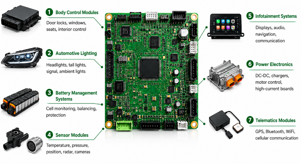
Custom PCB design for automotive means creating a circuit board that matches the electrical, thermal, mechanical, and production needs of a specific vehicle application, from control modules and BMS boards to lighting systems, radar PCBs, sensors, and power electronics.

At EBest Circuit (Best Technology), we support automotive PCB projects with DFM review, material and stackup suggestions, PCB fabrication, component sourcing, PCBA assembly, testing, and traceability, helping customers reduce design risks before production starts.

With our engineering-driven support and experience in high Tg FR4, heavy copper PCB, aluminum PCB, ceramic PCB, Rogers high-frequency PCB, and automotive-related quality control, we help customers move from prototype to stable production. If you are developing an automotive PCB project and need technical feedback before manufacturing, you can send your files or requirements to sales@bestpcbs.com for review.

Custom PCB Design for Automotive

What Is Custom PCB Design for Automotive?

Custom PCB design for automotive means designing a PCB for a specific vehicle application. At the same time, the board must be ready for manufacturing, assembly, inspection, and stable production.

Automotive PCBs are used in lighting modules, BMS boards, radar modules, sensors, cameras, power control units, charging systems, and ADAS products. These boards often work in tough conditions. They may face heat, vibration, moisture, high current, and electrical noise. Therefore, automotive PCB design must be planned with care.

Custom PCB Design for Automotive

What Quality Standards Should Custom PCB Design for Automotive Follow?

Automotive PCB projects need strict quality control. Even a small PCB problem can affect system performance or long-term reliability.

One common standard is IATF 16949. It is not a PCB layout rule. Instead, it is a quality management standard for automotive production. It helps control process stability, traceability, supplier quality, and corrective actions.

In addition, automotive PCB projects may follow IPC standards, ISO systems, material rules, and customer-specific requirements.

Standard or RequirementWhy It Matters
IATF 16949Supports automotive quality control and process stability
ISO 9001Builds a basic quality system for production
IPC-A-600Defines bare PCB acceptance requirements
IPC-A-610Defines PCBA acceptance requirements
IPC-6012 / IPC-6013Supports rigid PCB and flexible PCB performance
RoHS / REACHSupports material compliance
Customer RequirementsCovers special tests, marking, packaging, and traceability

Also, some customers may request extra reliability tests. These may include thermal cycling, vibration testing, humidity testing, solderability checks, impedance testing, and cross-section analysis.

As a result, a good supplier should do more than produce the board. It should also understand the quality path behind the project. This gives customers more confidence before prototype, trial production, and mass production.

What Engineering Documents Are Needed for Automotive PCB Production?

Automotive PCB production often needs more documents than standard PCB orders. These documents help both sides confirm the same requirements before production starts.

For early prototypes, the document package can be simple. However, for automotive production, customers may need more formal records.

Gerber Files and Fabrication Drawing

  • These files define copper layers, drill data, board outline, tolerances, copper thickness, surface finish, material, and special notes.

Stackup Drawing

  • This shows the layer structure, dielectric thickness, copper weight, impedance layers, and reference planes. It is important for high-speed, RF, and EMI-sensitive designs.

BOM and Assembly Drawing

  • For PCBA projects, the BOM and assembly drawing confirm part numbers, placement, polarity, package size, and assembly needs.

DFM Report

  • A DFM report shows possible manufacturing risks before production. It may cover trace width, spacing, hole size, via design, copper balance, solder mask clearance, and panelization.

APQP

  • APQP means Advanced Product Quality Planning. It helps plan quality before production. For automotive PCB projects, it can cover material choice, process planning, testing needs, and production control.

FMEA

  • FMEA helps review possible failure risks. For PCB projects, it may cover open circuits, short circuits, via cracks, plating issues, solder defects, thermal stress, and wrong components.

Control Plan

  • A control plan lists what must be checked during production. It can include board thickness, copper thickness, hole size, impedance, surface finish, AOI, E-test, X-ray, and final inspection.

PPAP

  • PPAP means Production Part Approval Process. It helps prove that the production process can meet customer requirements. It may include design records, process flow, FMEA, control plan, test results, sample approval, and inspection reports.

FAI Report

  • First Article Inspection checks the first sample against the approved drawing, files, and specifications.

These documents reduce confusion. Also, they help customers move from samples to stable production with better control.

How Does EBest Circuit Support Custom PCB Design for Automotive with DFM Review?

DFM review is one of the most useful steps before PCB fabrication. It helps find design risks before they become production problems.

EBest Circuit (Best Technology) supports custom PCB design for automotive with practical DFM review before fabrication and assembly. The goal is to improve manufacturability, reduce redesign work, and prepare the project for production.
During DFM review, EBest Circuit can check:

  • Trace width and spacing
  • Drill size and annular ring
  • Via type and via reliability
  • Copper thickness and current capacity
  • Impedance design and stackup feasibility
  • Solder mask clearance
  • Pad size and footprint accuracy
  • Thermal relief design
  • High-current copper areas
  • Panelization method
  • Surface finish choice
  • SMT and DIP assembly risks

For example, a power board may need thicker copper and better heat paths. A radar PCB may need controlled impedance and stable materials. A lighting PCB may need an aluminum base or copper base. Also, a BMS board may need proper spacing, isolation, and traceability.

In addition, EBest Circuit can review the project from both PCB and PCBA angles. This is useful because many problems appear between fabrication and assembly. With PCB manufacturing, component sourcing, assembly, and testing support in one place, customers can reduce communication work and speed up the project.
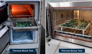
How to Choose Materials and Stackups for Custom PCB Design for Automotive?

Material and stackup choices affect automotive PCB reliability. The right choice depends on working temperature, current load, signal speed, board size, and cost target.

  • For many control boards, high Tg FR4 is a practical choice. It offers better heat resistance than standard FR4. Therefore, it is often used in sensors, control modules, interior electronics, and general vehicle electronics.
  • For power boards, heavy copper PCB may be better. Thick copper helps carry higher current and spread heat. It is often used in BMS boards, motor control boards, DC-DC converters, and charging systems.
  • For LED lighting and power modules, aluminum PCB or copper-based PCB can improve heat transfer. These materials help move heat away from LEDs and power components.
  • For high-power or high-temperature applications, ceramic PCB may be considered. Alumina, aluminum nitride, and silicon nitride can offer stronger thermal performance.
  • For radar, antenna, and high-frequency modules, Rogers or other RF materials may be used. These materials help reduce signal loss and support stable frequency performance.
PCB MaterialCommon Automotive Use
High Tg FR4Control modules, sensors, general vehicle electronics
Heavy Copper PCBBMS, motor control, power boards, charging systems
Aluminum PCBLED headlights, tail lights, lighting modules
Copper-Based PCBHigher power lighting and thermal products
Ceramic PCBPower modules and high-temperature applications
Rogers RF MaterialRadar, antenna, RF, and high-frequency boards

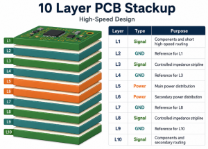
Also, stackup design should support both performance and production. Engineers should review layer count, ground planes, power planes, impedance, copper balance, thermal path, board thickness, and spacing.

The best material is not always the most expensive one. Instead, it should match the application, reliability target, and production budget.

What Testing and Inspection Are Needed for Automotive Custom PCBs?

Testing and inspection help confirm that automotive custom PCBs meet the approved requirements. They also help find issues before system testing or mass production.

The test plan depends on the project. A simple control PCB may need standard electrical testing and visual inspection. However, a high-reliability automotive PCB may need more checks and records.

Testing or Inspection MethodPurpose
AOIChecks line defects, shorts, opens, and surface issues
E-testConfirms electrical continuity and isolation
X-ray InspectionChecks hidden solder joints, BGAs, and internal risks
Impedance TestingConfirms controlled impedance requirements
Cross-Section AnalysisChecks plating, hole wall quality, and internal structure
Solderability TestingConfirms pad soldering performance
Thermal CyclingChecks reliability under temperature change
Functional TestingConfirms that the assembled board works correctly
FAIChecks the first sample against approved requirements
Traceability CheckLinks materials, batches, process steps, and inspection records
  • For PCBA projects, assembly inspection is also important. Solder paste printing, component placement, reflow profile, polarity, solder joints, and cleaning can all affect reliability.
  • In addition, traceability is important for automotive projects. Customers may need material batches, inspection records, production dates, component sources, and shipment details. Good traceability helps both sides respond faster if a quality question appears later.

EBest Circuit can support PCB fabrication, component sourcing, PCBA assembly, and testing. Therefore, customers can manage more steps through one supplier and reduce communication gaps.

Custom PCB Design for Automotive

Why Work with EBest Circuit for Automotive Custom PCB Design and Manufacturing?

Choosing an automotive PCB supplier is not only about price. Customers also need engineering support, material knowledge, quality control, testing ability, and stable production.

EBest Circuit (Best Technology) supports automotive PCB projects from design review to fabrication, assembly, testing, and production follow-up.

DFM Support Before Production

  • EBest Circuit reviews design files before fabrication. This helps customers find risks in spacing, vias, copper, stackup, solder mask, impedance, and assembly.
Multiple PCB Technologies

  • EBest Circuit can support FR4 PCB, high Tg PCB, heavy copper PCB, aluminum PCB, copper-based PCB, ceramic PCB, Rogers high-frequency PCB, and rigid-flex PCB.

Prototype to Mass Production Support

  • Customers can start with samples, improve the design, move to small batches, and then prepare for mass production. As a result, the project path becomes clearer.

PCB and PCBA One-Stop Service

  • EBest Circuit can provide PCB fabrication, component sourcing, SMT assembly, DIP assembly, testing, and box-build support. This helps customers reduce supplier coordination work.

Automotive Quality Support

  • With quality systems such as ISO 9001 and IATF 16949, EBest Circuit can support automotive-related quality needs. The team can also work with customers on inspection records, testing plans, and traceability.

Testing and Traceability

  • AOI, X-ray, E-test, impedance testing, functional testing, first article checks, and batch traceability can be arranged based on project needs.

Material and Stackup Suggestions

  • EBest Circuit can help customers choose practical materials and stackups based on heat, current, signal speed, reliability, and cost.

If you are developing automotive control modules, LED lighting boards, BMS boards, radar PCBs, sensor boards, power boards, or communication modules, EBest Circuit can help review the files and support production.

To discuss your project, pls feel free to send Gerber files, BOM, drawings, stackup needs, application details, and target quantity to sales@bestpcbs.com.

FAQs About Custom PCB Design for Automotive

What makes custom PCB design for automotive different from normal PCB design?
It must consider heat, vibration, EMI, EMC, current load, material stability, testing, documents, and traceability. These needs are higher than many standard PCB projects.

Does every automotive PCB project need IATF 16949 support?
Not always. Early prototypes may not need full automotive documentation. However, production projects often benefit from IATF 16949 quality control.

What files should I provide for quotation?
You should provide Gerber files, drill files, stackup details, fabrication drawing, BOM, pick-and-place file, assembly drawing, impedance needs, copper thickness, surface finish, test needs, and target quantity.

Can EBest Circuit help if my design is not ready for production?
Yes. We can review your Gerber files, BOM, drawings, and stackup from a manufacturing point of view. Our team can provide DFM suggestions on material choice, copper thickness, drilling, solder mask, panelization, surface finish, controlled impedance requirements, and assembly risks. We do not replace circuit design or PCB layout work, but we help make the design more ready for fabrication, PCBA assembly, and production.

What materials are used in automotive custom PCBs?
Common options include high Tg FR4, heavy copper PCB, aluminum PCB, copper-based PCB, ceramic PCB, and Rogers high-frequency material. The right choice depends on the application.

Does automotive PCB production need PPAP?
Some production projects may need PPAP, especially when the PCB enters a formal automotive supply chain. The need depends on customer requirements and project risk.

Can one supplier handle PCB fabrication and PCBA assembly?
Yes. A one-stop supplier can manage PCB fabrication, component sourcing, assembly, inspection, testing, and traceability. This helps reduce communication gaps.

How can I start a custom automotive PCB project with EBest Circuit?
You can send your Gerber files, BOM, drawings, technical requirements, and application details to sales@bestpcbs.com. EBest Circuit can review your files and provide DFM, material, fabrication, assembly, and testing support.

You may also like

RF Microwave PCB: Design, Materials, Fabrication, and Manufacturer Guide

May 21st, 2026

How can an RF microwave PCB keep high-frequency signals stable when small design and fabrication changes may affect the final result? This guide explains how RF microwave PCB boards work, how to choose suitable materials, how to control impedance and signal loss, and how to select the right manufacturer for prototype and production projects.

EBest Circuit (Best Technology) is an engineering-driven PCB and PCBA manufacturer with over 20 years of experience supporting high-frequency, RF, microwave, automotive, medical, industrial, communication, and aerospace/UAV projects. With self-owned PCB and PCBA factories, EBest provides DFM review, material selection support, controlled impedance PCB fabrication, component sourcing, assembly, testing, and production-quality support from prototype to mass production.

If you are evaluating an RF microwave PCB project and need practical manufacturing feedback, you can send your Gerber files, stackup, material requirements, and quantity to sales@bestpcbs.com for a technical review and quotation.

RF Microwave PCB

What Is an RF Microwave PCB Board?

An RF microwave PCB board is a printed circuit board made for radio frequency and microwave signals. It is a high-frequency circuit board designed for RF and microwave signal transmission, usually covering applications from MHz-level RF circuits to GHz and millimeter-wave systems.

In simple terms, RF board PCB is a broader category for radio-frequency circuits, microwave PCB usually refers to higher-frequency GHz-range circuits, and RF microwave PCB board is often used to describe a low-loss, impedance-controlled PCB built for both RF and microwave performance.

Unlike a standard FR4 PCB, an RF microwave PCB is part of the signal path. Therefore, the board does more than connect components. It also affects signal speed, loss, phase, reflection, and radiation.

In many low-speed PCB designs, small material changes may not create serious issues. However, RF and microwave circuits are more sensitive. A small shift in dielectric thickness, copper roughness, or trace width can change the final electrical behavior.

RF microwave PCB boards are commonly used in:

  • 5G communication modules
  • RF antennas
  • Radar systems
  • Satellite communication equipment
  • Aerospace and UAV electronics
  • Industrial RF systems
  • Medical RF devices
  • Automotive radar and sensing modules
  • High-frequency test instruments
RF Microwave PCB

As a result, RF microwave PCB design must start with clear electrical goals. These goals may include low insertion loss, stable impedance, low return loss, strong grounding, and repeatable batch performance.

A well-built RF microwave PCB helps engineers reduce signal loss and improve circuit stability. It also makes the product easier to move from prototype to mass production.

How Does an RF Microwave High-Frequency PCB Work?

An RF microwave high-frequency PCB works by guiding electromagnetic energy through controlled signal paths. These paths may include microstrip lines, stripline traces, coplanar waveguides, grounded coplanar waveguides, and antenna feed lines.

At high frequencies, a copper trace is not just a simple wire. Instead, it works as a transmission line. The signal travels through both the copper and the surrounding dielectric field. Because of this, the material, trace width, spacing, ground plane, and via structure all affect performance.

Several factors matter most.

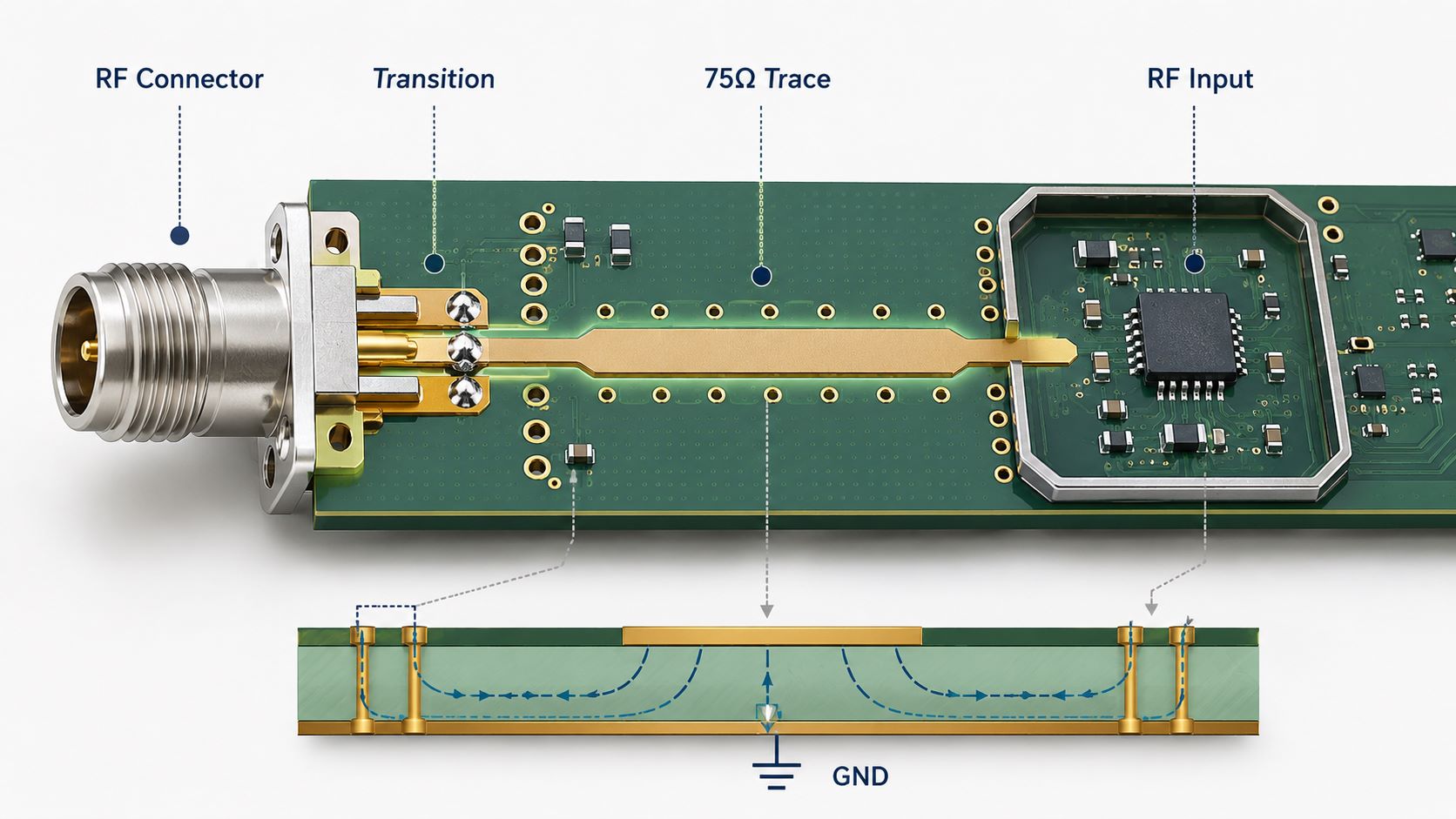
  • Impedance control is one of the first concerns. Many RF circuits use 50 ohm impedance, although some designs use other values. The final impedance depends on trace width, copper thickness, dielectric thickness, and dielectric constant.
  • Insertion loss is also important. It shows how much signal power is lost as the signal moves through the board. Loss can come from the dielectric material, copper surface, radiation, and poor transitions.
  • Return loss shows how much signal reflects back. Poor layout, sudden trace width changes, bad via design, or weak connector launch design may increase reflection.
  • Phase stability matters in radar, antenna, and communication systems. If the material or process changes too much, phase behavior may shift. This can affect signal timing and accuracy.
  • Ground return path is another key factor. RF current needs a clean return path. Therefore, a continuous ground plane and proper via stitching can help reduce noise, coupling, and radiation.

In short, an RF microwave PCB works well when the signal sees a stable path from the source to the load. Good design creates that path. Good fabrication keeps it consistent.

Where Are RF Microwave PCB Boards Used in 24GHz, 5G, and High-Power Applications?

RF microwave PCB boards are used in products where frequency, bandwidth, signal loss, and stability matter. Some boards are small antenna modules. Others are complex multilayer boards for communication systems.

Application AreaTypical RequirementPCB Focus
24GHz radarStable detection and low signal driftLow-loss laminate, precise impedance, antenna accuracy
5G RF modulesHigh bandwidth and stable transferStable Dk/Df, fine-line control, hybrid stackup
RF antennasGood radiation efficiencyAntenna geometry, copper tolerance, surface finish
Base stationsLong-term signal reliabilityThermal control, material consistency, multilayer control
Aerospace and UAVLightweight and stable RF performanceTraceability, process control, vibration resistance
Industrial RF equipmentReliable field operationStrong structure, thermal reliability, test control
High-power RF modulesHeat control and signal stabilityMetal-backed structure, thermal path, copper control
  • For a 24GHz RF microwave PCB, material choice and layout precision are already important. As the frequency rises, small geometry changes become more visible in actual RF performance.
  • For 5G-ready RF microwave high-frequency PCB fabrication, engineers often need low transmission loss, stable dielectric properties, and repeatable production. In many cases, they also need hybrid stackups. These stackups combine RF materials with FR4 or other support layers.
  • Meanwhile, high-power RF applications add another challenge: heat. These boards may need metal-backed structures, thermal vias, heavy copper areas, or a dedicated heat path.

Therefore, the best RF microwave PCB is not always the most complex board. It is the board that fits the signal, thermal, mechanical, and production needs of the product.

How to Do PCB Material Selection for RF Microwave Millimeter-Wave Design?

Material selection is one of the most important steps in RF microwave PCB design. The laminate affects signal loss, impedance, phase stability, heat control, and long-term reliability.

For PCB material selection for RF microwave millimeter-wave design, engineers usually check several material properties.

Material FactorWhy It Matters
Dielectric constant, DkAffects trace width, impedance, wavelength, and phase speed
Dissipation factor, DfAffects dielectric loss, especially at high frequency
Copper roughnessAffects conductor loss and signal attenuation
Thermal conductivityHelps move heat away from RF power areas
CTEAffects dimensional stability and via reliability
Moisture absorptionAffects dielectric stability and long-term use
Process compatibilityAffects drilling, lamination, routing, and yield

Common RF microwave PCB materials include Rogers high-frequency laminates, PTFE-based laminates, ceramic-filled hydrocarbon materials, Taconic materials, and other low-loss substrates.

However, the lowest-loss material is not always the best choice. The project may also need cost control, easy sourcing, stable production, and strong mechanical performance. Therefore, engineers should choose the material based on frequency, loss target, thermal need, stackup, volume, and budget.

In some projects, a hybrid stackup is a practical choice. For example, the RF layer may use a low-loss material, while the support layers use FR4. This helps reduce cost while keeping the high-frequency path stable.

Before production, the material choice should be reviewed with the manufacturer. This can help avoid problems with drilling, lamination, copper control, and dimensional stability.

What Are the Main RF Microwave PCB Board Design and Layout Rules?

Good RF microwave PCB board design and layout starts with a clean signal path. The layout should reduce loss, avoid sudden impedance changes, and give RF signals a stable return path.

Here are the main design rules.

Keep RF traces short and direct.

  • Shorter traces reduce loss and lower the risk of unwanted coupling. Also, avoid unnecessary stubs, long detours, and sharp changes in direction.

Control impedance from the start.

  • The stackup, copper thickness, dielectric thickness, and trace width should be planned before layout. This helps avoid later redesign.

Use a continuous ground plane.

  • A broken ground plane can disturb the return path. As a result, it may increase radiation and impedance mismatch.

Add ground via stitching where needed.

  • Ground vias near RF traces can help control the electromagnetic field. They can also reduce coupling between nearby circuits.

Pay attention to via transitions.

  • At high frequency, a via can create unwanted inductance and capacitance. Therefore, via size, pad size, anti-pad size, and via depth should be reviewed.

Separate noisy circuits from RF areas.

  • Power converters, digital clocks, and fast switching signals should stay away from sensitive RF paths. In addition, proper shielding and layer planning can reduce noise.

Review solder mask over RF traces.

  • Solder mask can change impedance because it adds material above the copper. Some RF designs need solder mask clearance over controlled traces.

Design connector launches carefully.

  • A poor RF connector launch can create reflection and loss. Therefore, the launch area should match the connector type, stackup, and target impedance.

Overall, RF layout is not only about routing traces. It is about building a stable electrical environment around each signal path.

What Pain Points Come With RF Microwave PCB, and How Does EBest Solve Them?

RF microwave PCB projects often face issues that are not obvious at first. A board may look correct, but still fail RF testing. Therefore, early review and stable fabrication control are important.

Customer ChallengeWhat Usually HappensHow EBest Supports the Project
Material choice is unclearThe customer knows the frequency, but not the best laminateEBest reviews frequency, Dk/Df, stackup, heat, cost, and production volume before giving material suggestions
Impedance is hard to controlSmall trace or dielectric changes may cause reflectionEBest supports controlled impedance fabrication and checks stackup, trace width, copper thickness, and impedance targets before production
Prototype results are hard to repeatThe first sample may work, but later batches may shiftEBest helps control material batches, etching, lamination, inspection, and process records
Hybrid stackups create process riskRF material and FR4 may behave differently during laminationEBest reviews hybrid stackup feasibility and gives DFM suggestions before fabrication
RF designs need PCB and assembly supportCustomers may need bare boards, components, assembly, and testingEBest provides PCB fabrication, component sourcing, PCBA assembly, and testing support under one workflow
Design files are not production-readySmall layout issues may lead to delay or reworkEBest provides DFM pre-review to help customers find risks before the board enters production

This structure keeps the problem and solution clear. It also helps buyers quickly see whether the manufacturer can support real project risks.

For RF microwave PCB projects, EBest does not only build boards from files. Instead, the engineering team can help review the practical manufacturing side of the design. This includes material selection, stackup, impedance control, trace tolerance, via design, and assembly needs.

As a result, customers can reduce trial-and-error during prototyping. They can also move more smoothly from sample builds to volume production.

How Does RF Microwave PCB Fabrication Control Impedance, Loss, and Tolerance?

RF microwave PCB fabrication requires stable process control. The goal is to keep the finished board close to the original electrical design.

Several fabrication steps affect RF performance.

Material handling

  • High-frequency materials may need special storage, drilling, lamination, and routing control. Good handling helps keep the material stable.

Stackup control

  • Dielectric thickness affects impedance. Therefore, prepreg flow, lamination pressure, and material selection must stay consistent.

Etching control

  • Trace width affects impedance and signal loss. The manufacturer must understand copper thickness and etching behavior. Then, it can apply proper compensation.

Copper thickness control

  • Uneven copper can change impedance. It can also affect conductor loss. Stable plating helps improve consistency.

Drilling and via quality

  • Vias affect RF transitions and board reliability. Clean drilling, proper desmear, and stable copper plating are important.

Surface finish selection

  • ENIG, immersion silver, OSP, and other finishes may affect solderability and surface behavior. The right finish depends on RF needs, assembly process, storage time, and customer standards.

Impedance testing

  • TDR testing and impedance coupons help confirm whether the board meets the target. This is especially important for controlled impedance RF circuits.

AOI and electrical testing

  • AOI checks trace quality and pattern accuracy. Electrical testing checks opens and shorts before shipment.

Because of these factors, a low-loss material alone cannot ensure good RF performance. The fabrication process must also be stable. In addition, the manufacturer must understand how each process step affects the final signal path.

How to Choose the Right RF Microwave PCB Manufacturer?

Choosing the right RF microwave PCB manufacturer is both a purchasing decision and an engineering decision. The supplier’s skill can affect signal performance, production yield, and delivery stability.

A reliable RF microwave PCB supplier should provide:

  • Experience with high-frequency materials
  • Controlled impedance fabrication
  • DFM review before production
  • Stackup and material support
  • Stable material sourcing
  • Prototype and small-batch support
  • Repeatable production control
  • AOI, electrical testing, and impedance testing
  • Clear communication about tolerance and process limits
  • Support for overseas customers

When requesting RF microwave PCB production quotes, customers should prepare clear data.

Required InformationWhy It Matters
Gerber filesAllows the manufacturer to review the board accurately
StackupHelps confirm impedance and lamination structure
Material typeAffects cost, lead time, and RF performance
Copper thicknessAffects impedance and current capacity
Board thicknessAffects mechanics and signal structure
Surface finishAffects assembly and solderability
Impedance targetSupports controlled impedance fabrication
QuantityAffects pricing and delivery plan
Testing needsHelps define inspection scope
Assembly needsHelps plan PCB and PCBA together

A good manufacturer should not only quote the lowest price. It should also find material, design, process, or assembly risks before production. For RF microwave projects, this early review can save time and reduce avoidable cost.

Why EBest Is the Trusted RF Microwave PCB Partner for Global Brands?

EBest Circuit (Best Technology) supports customers that need reliable RF microwave PCB manufacturing from prototype to production. The company provides PCB fabrication, component sourcing, PCBA assembly, testing, and turnkey electronics manufacturing.

For RF microwave PCB projects, EBest’s value is not only in board production. It also comes from engineering support before production starts.

Engineering-driven review

  • EBest provides DFM pre-review for material choice, stackup, impedance, copper thickness, trace width, via structure, and manufacturability.

High-frequency material experience

  • The team supports Rogers and other low-loss laminates. It can also support hybrid stackups when customers need a balance of RF performance and cost.

PCB and PCBA support

  • Many RF products need more than bare PCB fabrication. Therefore, EBest can support component sourcing, SMT assembly, testing, and final production coordination.

Quality system support

  • EBest works with quality systems suitable for demanding industries, including ISO9001, ISO13485, IATF16949, AS9100D, and UL-related PCB manufacturing support depending on project needs.

Prototype to mass production

  • RF products often move through several validation stages. EBest supports quick prototyping, small-batch builds, and production orders. This helps customers keep the same manufacturing logic across the project.

Industry experience

  • EBest serves communication, medical device, industrial control, automotive electronics, aerospace/UAV, lighting, robotics, new energy, and instrument applications.

For customers looking for a reliable RF microwave PCB manufacturer, EBest can review design files, support material selection, provide fabrication suggestions, and offer production quotes based on real project needs.

RF Microwave PCB

To discuss an RF microwave PCB project, customers can contact sales@bestpcbs.com with Gerber files, stackup, material requirements, quantity, and assembly needs.

FAQs About RF Microwave PCB

What is the difference between RF PCB and microwave PCB?
RF PCB is a broad term for boards that carry radio frequency signals. Microwave PCB usually refers to boards that work at higher frequencies. In many searches, the term RF microwave PCB covers both types.

What materials are commonly used for RF microwave PCB fabrication?
Common materials include Rogers laminates, PTFE-based laminates, ceramic-filled hydrocarbon materials, low-loss RF substrates, and hybrid RF plus FR4 stackups.

Can RF microwave PCB be used for 24GHz and 5G applications?
Yes. RF microwave PCB boards can be used in 24GHz radar, 5G RF modules, antennas, communication systems, and high-frequency sensing products. Here, 24GHz usually refers to radar applications, while 2.4GHz is more commonly used for WiFi, Bluetooth, Zigbee, and other ISM-band wireless devices.

Where can I get metal-backed RF microwave PCB boards?
You can get metal-backed RF microwave PCB boards from manufacturers with both RF material experience and thermal management capability.

EBest Circuit (Best Technology) can provide metal-backed RF microwave PCB boards using aluminum or copper base structures to support heat dissipation in high-power RF and microwave applications. For projects that need low-loss materials, controlled impedance, and stable thermal performance, EBest can also support DFM review, material selection, PCB fabrication, assembly, and testing.

Does RF microwave PCB require controlled impedance?
In most cases, yes. Controlled impedance helps reduce reflection and signal loss. Many RF traces use 50 ohm impedance, but the final value depends on the circuit design.

Can EBest support RF microwave PCB assembly?
Yes. EBest supports RF microwave PCB fabrication, component sourcing, SMT assembly, testing, and turnkey electronics manufacturing.

How do I request RF microwave PCB production quotes?
Prepare Gerber files, stackup, material type, copper thickness, board thickness, surface finish, impedance target, quantity, and assembly needs. Clear data helps the manufacturer quote faster and more accurately.

If you are not sure whether your RF microwave PCB design is ready for production, EBest Circuit (Best Technology) can review your files and provide practical manufacturing feedback. You can send your Gerber files and project requirements to sales@bestpcbs.com for a technical review and quotation.

You may also like

High Frequency PCB for Automotive Radar: Practical Design and Manufacturing Guide for 77GHz Radar Modules

May 20th, 2026

How can high frequency PCB for automotive radar help reduce signal loss and improve 77GHz ADAS module stability? In automotive radar design, small changes in material, stackup, antenna geometry, or impedance can affect detection range and signal consistency. This guide explains the practical PCB factors that influence radar performance, from material selection and DFM review to surface finish, reliability control, and mass production support.

High Frequency PCB for Automotive Radar

How Does a High Frequency PCB for Automotive Radar Work in a 77GHz Radar Module?

A high frequency PCB inside a 77GHz radar module is not only used to connect components. It also supports RF signal transmission, antenna behavior, grounding, power distribution, and mechanical integration inside the radar housing. Because the radar signal works at millimeter-wave frequency, the PCB structure becomes part of the signal path.

  • It transfers RF signals from the radar IC to the antenna area
    The radar transceiver generates high-frequency signals. These signals move through microstrip lines, stripline structures, feedlines, vias, and antenna networks on the PCB. At 77GHz, even a small change in line width, dielectric thickness, or copper surface condition may affect insertion loss and impedance.
  • It may form the antenna directly on the board
    Many automotive radar modules use PCB antenna arrays. In this design, antenna patches or antenna feed networks are created by copper patterns. The PCB manufacturer is not just fabricating copper traces. It is producing a functional RF structure.
  • It helps receive reflected signals
    Radar signals are transmitted outward and reflected by vehicles, pedestrians, road barriers, or nearby objects. The receiving antenna collects the reflected signal and routes it back to the radar IC. The radar system then calculates distance, speed, angle, and movement.
  • It provides a stable ground reference
    Ground layers are critical in radar PCB design. A continuous ground plane helps reduce unwanted radiation, signal reflection, and noise coupling. If the ground path is broken or poorly connected, the RF path may become unstable.
  • It supports power, digital, and interface circuits
    A radar PCB may also include power management circuits, MCU or DSP control sections, CAN interface, Ethernet interface, shielding contacts, and connectors. These areas should be arranged carefully to avoid interference with sensitive RF sections.
  • It must fit the radar enclosure
    The PCB must match the radar housing, radome, connector position, screw holes, thermal path, and shielding cover. Poor mechanical matching may create stress, warpage, or assembly difficulty.

In short, the board is part of the radar system. Good PCB design helps the radar module perform more consistently during testing, assembly, and long-term vehicle operation.

Where Is High Frequency PCB Used in Automotive Radar Applications?

High frequency PCB is used in different radar positions around the vehicle. Each position has different requirements for detection range, field of view, module size, antenna arrangement, and environmental reliability. That is why one radar PCB design may not be suitable for all automotive radar applications.

  • Front long-range radar
    Front radar is commonly used for adaptive cruise control, forward collision warning, and automatic emergency braking. These modules need stable long-distance signal transmission. The PCB should offer low RF loss, accurate antenna geometry, and good phase consistency.
  • Corner radar
    Corner radar is used for blind spot detection, lane change assistance, and cross-traffic alert. These modules are usually compact, so the PCB needs efficient antenna layout and controlled RF routing in a limited space.
  • Rear radar
    Rear radar supports reverse warning, rear collision detection, and parking assistance. The PCB must maintain stable performance in environments where moisture, vibration, dust, and temperature changes may occur.
  • Short-range radar
    Short-range radar is often used for parking systems and nearby object detection. The PCB may require dense antenna structures and precise copper pattern control because the module needs accurate short-distance sensing.
  • In-cabin radar
    In-cabin radar can be used for occupant sensing, child presence detection, and gesture recognition. These boards often need compact layout, controlled radiation behavior, and good compatibility with plastic housings.
  • Advanced imaging radar
    Imaging radar requires more channels and higher signal processing capability. The PCB may need tighter phase control, more complex routing, and better production repeatability.

For all these applications, the PCB must do more than meet basic electrical continuity. It must support stable radar sensing under real vehicle conditions.

What PCB Material Should Be Used for 77GHz Automotive Radar?

Material selection is one of the most important decisions in a high frequency PCB for automotive radar. The substrate controls dielectric loss, signal speed, antenna resonance, impedance behavior, and long-term stability. A material that works well for ordinary control circuits may not be suitable for 77GHz RF transmission.

  • Low-loss high-frequency laminate is usually required for the RF area
    At 77GHz, dielectric loss becomes a major concern. A low-loss material helps reduce signal attenuation from the radar IC to the antenna. This is especially important for front radar and long-range sensing.
  • Stable Dk helps maintain predictable antenna behavior
    Dk means dielectric constant. If Dk changes too much with frequency, temperature, or production batch, the antenna and RF traces may behave differently from the design model. Stable Dk helps keep the radar frequency response more predictable.
  • Low Df helps reduce energy loss
    Df means dissipation factor. Lower Df usually means lower dielectric loss. For millimeter-wave radar, this helps preserve signal strength and improve RF efficiency.
  • Copper foil type should be reviewed
    Copper roughness matters at high frequency. Rougher copper may increase conductor loss. For sensitive RF feedlines and antenna areas, smoother copper can support more consistent signal transmission.
  • FR4 can be used only in non-critical areas
    FR4 may be suitable for digital control, power circuits, or mechanical support layers. However, it is usually not a good choice for 77GHz antenna and RF feedline areas because its dielectric properties are not stable enough for high-performance millimeter-wave transmission.
  • Hybrid stackup is common in radar modules
    Many radar boards combine high-frequency laminate for the RF layer with FR4 for digital or power layers. This can reduce total cost while keeping the RF area stable.
  • Material availability matters for mass production
    A material may perform well in prototype, but if it is difficult to source consistently, it may create problems later. Engineers should confirm material availability before approving the design for production.

A practical material choice should balance RF performance, cost, manufacturability, reliability, and supply stability.

How Should the PCB Stackup Be Designed for Automotive Radar?

Stackup design controls how copper layers, dielectric materials, ground planes, and signal paths work together. For automotive radar, stackup is not just a mechanical layer arrangement. It directly affects RF performance, antenna behavior, impedance control, warpage, and assembly quality.

  • Place the RF antenna layer carefully
    Many radar modules place the antenna on the top layer. This makes copper geometry, surface finish, and solder mask control very important. If the antenna layer is changed later, the radar performance may need to be revalidated.
  • Control dielectric thickness tightly
    The distance between the antenna copper and ground plane affects antenna resonance and impedance. Loose dielectric thickness tolerance may cause frequency shift or inconsistent signal behavior.
  • Use a continuous ground reference layer
    A stable ground plane helps control RF return current and reduce unwanted coupling. Ground voids, splits, or poorly connected areas may create unpredictable RF results.
  • Review hybrid lamination carefully
    If the board combines high-frequency laminate and FR4, the manufacturer must check bonding strength, thermal expansion difference, lamination pressure, and warpage risk.
  • Keep the structure balanced
    A symmetrical or well-balanced stackup helps reduce board bending. This is important for SMT assembly, radar IC mounting, shielding installation, and final module assembly.
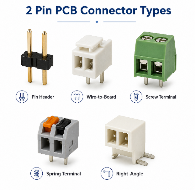
  • Manage RF vias and transitions
    Poor via transitions can create impedance discontinuity. Long via stubs, weak grounding, or uncontrolled launch structures may reduce signal quality.
  • Separate RF, digital, and power areas
    Switching power circuits and digital signals should be kept away from sensitive RF paths. Proper layer planning helps reduce coupling and noise.
  • Keep the approved stackup unchanged after validation
    Once a radar board passes RF validation, changes to material, dielectric thickness, copper type, or layer sequence should be controlled carefully.

A good stackup design reduces the gap between simulation, prototype testing, and real production results.

Why Is Antenna Area Control Critical in Automotive Radar PCB Manufacturing?

The antenna area is one of the most sensitive regions on a high frequency PCB for automotive radar. When the antenna is formed directly by copper patterns, the PCB manufacturer is effectively producing the radar’s transmitting and receiving structure. This area needs much tighter control than ordinary signal routing.

  • Antenna dimensions affect frequency response
    If the antenna patch is slightly larger or smaller than designed, the antenna response may shift. Over-etching or under-etching can change the effective antenna size.
  • Feedline accuracy affects matching
    The feedline connects the radar IC to the antenna. If the line width or spacing changes, impedance may shift and signal reflection may increase.
  • Element spacing affects phase consistency
    Radar antenna arrays depend on consistent spacing between antenna elements. Uneven spacing may affect angle detection and beam behavior.
  • Solder mask can change the dielectric environment
    If solder mask covers an area that should remain open, it may change local capacitance and dielectric loading. This can affect antenna performance.
  • Surface finish may influence RF behavior
    Different finishes have different metal layers and thicknesses. In sensitive antenna regions, the finish should be selected and controlled carefully.
  • Layer alignment must be controlled
    The antenna layer and reference ground layer need proper alignment. Misregistration may affect the RF field and antenna behavior.
  • Panelization can influence consistency
    The position of the board inside the production panel may affect etching uniformity. For radar antenna arrays, the manufacturer should consider whether the panel layout creates dimensional variation.

Before production, the drawing should clearly define antenna tolerance, solder mask opening, copper thickness, surface finish, inspection points, and RF keep-out areas.

How Does Controlled Impedance Affect Radar Signal Transmission?

Controlled impedance helps RF signals travel through the PCB with predictable behavior. If impedance changes along the signal path, part of the signal may reflect back. In radar modules, this can increase loss, reduce signal quality, and make calibration more difficult.

  • Trace width must match the stackup
    A 50-ohm RF line depends on trace width, dielectric thickness, copper thickness, and material Dk. The manufacturer should calculate the line width based on real material data.
  • Etching tolerance affects impedance
    If the finished trace is narrower or wider than expected, impedance changes. For 77GHz designs, this variation can be significant.
  • Reference plane distance must be stable
    The distance between RF trace and ground layer controls impedance. If dielectric thickness varies, impedance may drift.
  • Solder mask condition should be confirmed
    Whether the RF trace is covered by solder mask or exposed can affect impedance. This should be defined before production.
  • Vias and bends need special attention
    RF vias, bends, launch structures, and transitions may create discontinuity. Smooth transitions help reduce reflection.
  • Impedance coupons may be required
    Test coupons help verify whether the fabricated board meets impedance requirements. They are useful for production control.
  • Repeat orders must follow the approved process
    Material substitution, copper thickness change, or stackup change may alter impedance. Such changes should not be made without engineering review.

Controlled impedance is not a decoration on the drawing. It is a manufacturing requirement that directly affects radar signal stability.

High Frequency PCB for Automotive Radar

What Are the Main Manufacturing Challenges of Automotive Radar PCB?

Automotive radar PCB manufacturing is difficult because it combines millimeter-wave RF requirements with automotive-level consistency. The manufacturer must control fine copper features, hybrid materials, surface finish, flatness, and inspection records at the same time.

  • Fine RF trace etching
    Small RF lines and gaps need precise etching compensation. If the etching process is unstable, impedance and antenna geometry may shift.
  • Antenna copper accuracy
    Antenna patterns must match the design closely. Small copper deviations can affect resonance, gain, and phase response.
  • Hybrid material lamination
    High-frequency materials and FR4 may expand differently during lamination. This can create warpage, bonding stress, or registration issues.
  • Copper roughness control
    At 77GHz, the copper surface becomes important. The manufacturer should understand how copper foil type affects conductor loss.
  • Via plating quality
    Radar boards may include dense grounding vias and signal transitions. Poor via plating can reduce reliability and affect electrical performance.
  • Solder mask registration
    Mask shift near antenna or RF traces may change the local RF environment. Mask opening requirements must be followed accurately.
  • Board flatness
    Warpage can affect SMT assembly and module housing installation. A warped PCB may also create stress on radar ICs or connectors.
  • Surface finish consistency
    The finish must support both soldering and RF requirements. Inconsistent finish thickness may create assembly or performance concerns.
  • Batch repeatability
    Automotive customers need stable quality over time. The same material, process, and inspection method should be used from prototype to mass production.

The real challenge is not producing one good sample. It is producing stable boards again and again.

How Should DFM Review Be Done Before Automotive Radar PCB Production?

DFM review is a key step before producing a high frequency PCB for automotive radar. Many RF problems are hard to fix after the board has been fabricated. A good DFM review can identify risks before they become expensive prototype failures.

  • Check the material specification
    The manufacturer should confirm laminate brand, grade, thickness, copper type, and material availability. Any unclear material description should be clarified before quotation or production.
  • Review the stackup carefully
    Stackup review should include dielectric thickness, copper thickness, layer sequence, ground reference, and hybrid lamination feasibility.
  • Confirm impedance requirements
    The target impedance, tolerance, trace width, and test method should be confirmed. If the drawing only says “controlled impedance” without details, the manufacturer should ask for clarification.
  • Inspect the antenna area
    The antenna pattern should be reviewed for copper tolerance, solder mask opening, surface finish, and dimensional inspection needs.
  • Check solder mask rules
    RF traces and antenna patches may need larger solder mask clearance or complete mask opening. This should not be left to default factory rules.
  • Review via structures
    The manufacturer should check via placement, grounding vias, via stubs, via-in-pad risk, and plating requirements.
  • Confirm surface finish
    The finish should support both SMT assembly and RF performance. For sensitive RF areas, the finish selection may need extra review.
  • Evaluate copper balance and warpage risk
    Uneven copper distribution may cause board bending. Copper balancing should be reviewed without disturbing RF areas.
  • Review panelization
    Panel design should support stable etching, assembly handling, and antenna consistency.
  • Define inspection requirements
    AOI, impedance testing, electrical testing, microsection, dimensional inspection, and final inspection should be specified clearly.

A strong DFM review helps customers reduce avoidable errors and prepare the design for repeatable production.

What Surface Finish Is Suitable for Automotive Radar PCB?

Surface finish protects exposed copper and supports soldering. In automotive radar PCB, it may also affect RF performance, especially when antenna patterns or RF feedlines are exposed. The best finish depends on the antenna design, assembly process, storage time, and reliability requirements.

  • ENIG
    ENIG offers good solderability, flatness, and storage stability. It is commonly used in many PCB applications. However, the nickel layer should be reviewed when it appears in RF-sensitive areas.
  • Immersion silver
    Immersion silver provides a flat and conductive surface. It can be suitable for RF applications, but storage and handling conditions should be controlled to avoid tarnish or contamination.
  • OSP
    OSP is flat and simple. It avoids extra metal layers, which may be useful in some RF designs. However, it has shorter shelf life and requires careful assembly planning.
  • Immersion tin
    Immersion tin provides a flat solderable surface. It may be used in some designs, but process control and whisker risk should be considered.
  • Selective finish
    Some radar boards may need different treatment for antenna areas and component soldering pads. This should be clearly marked in the fabrication notes.

When selecting surface finish, we should consider:

  • Whether the antenna area needs exposed copper
  • Whether nickel is acceptable in RF areas
  • Whether the radar IC requires fine-pitch assembly
  • How long the boards will be stored before SMT
  • Whether the finish meets automotive reliability requirements
  • Whether drawing notes clearly separate RF and soldering areas

Surface finish should not be selected only for solderability. For radar boards, RF behavior and assembly reliability must be reviewed together.

How to Ensure Reliability for High Frequency PCB for Automotive Radar in Harsh Environments?

Automotive radar modules work in demanding environments. They may face high temperature, low temperature, vibration, humidity, dust, road salt, and long service life. The PCB must remain stable both electrically and mechanically.

  • Material traceability
    Material batch records should be kept for laminate, prepreg, copper foil, surface finish chemistry, and other key production materials.
  • Lamination process control
    Temperature, pressure, time, and bonding quality should be controlled during lamination. This is especially important for hybrid stackups.
  • Copper plating inspection
    Hole wall copper thickness and plating quality affect long-term reliability. Poor plating can create failures under thermal cycling or vibration.
  • Microsection analysis
    Microsection inspection helps verify plating, dielectric condition, layer registration, and lamination quality.
  • AOI inspection
    AOI helps detect open circuits, shorts, under-etching, over-etching, and copper pattern issues in RF and antenna areas.
  • Electrical testing
    Electrical testing confirms continuity and isolation. It is a basic but important step before shipment.
  • Impedance verification
    Impedance testing helps confirm that the RF transmission path matches design requirements.
  • Dimensional inspection
    Critical antenna dimensions should be inspected when required. This helps control RF consistency.
  • Solderability testing
    Surface finish quality should support reliable SMT assembly.
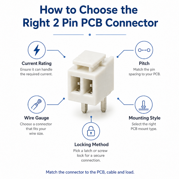
  • Ionic contamination control
    Cleanliness matters for long-term reliability. Residue on the board may create leakage or corrosion risk.
  • Warpage inspection
    Board flatness should be checked, especially when radar ICs, shields, or connectors require precise assembly.
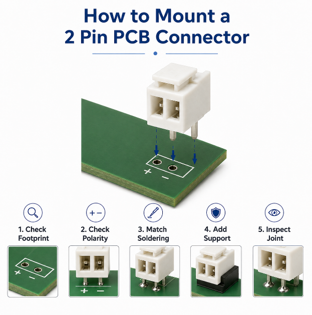
  • Documentation control
    Inspection reports, material records, and shipment traceability should be available for customer review.

Reliability is not created by one final test. It comes from stable material, controlled process, careful inspection, and complete documentation.

High Frequency PCB for Automotive Radar

How Can a Manufacturer Support High Frequency PCB for Automotive Radar Projects?

A qualified PCB manufacturer should support the project before production begins. For 77GHz radar PCB, early communication can help customers reduce design risk, control cost, and improve the chance of successful validation.

  • Material selection support
    The manufacturer can help compare high-frequency laminates based on Dk, Df, copper type, thickness, availability, and cost.
  • Stackup review
    The manufacturer can check whether the stackup supports impedance, antenna behavior, lamination, and board flatness.
  • Controlled impedance calculation
    Trace width should be calculated using real laminate data and finished copper thickness. This helps reduce mismatch between design and production.
  • DFM pre-check
    The manufacturer can review antenna areas, RF traces, solder mask openings, vias, surface finish, panelization, and assembly risks.
  • Prototype fabrication
    Prototype boards should be made with production-aware methods. This helps make later small-batch production smoother.
  • Small-batch production support
    After prototype validation, the manufacturer should keep the approved material, stackup, and process conditions stable.
  • Mass production consistency
    For automotive projects, consistency matters as much as capability. The manufacturer should maintain clear process records and inspection standards.
  • Inspection and testing support
    AOI, electrical testing, impedance testing, microsection, X-ray when required, and dimensional inspection help improve quality confidence.
  • Traceability support
    Material and production records help customers manage automotive quality requirements and future audits.
  • Assembly coordination
    Radar modules often require fine-pitch components, shields, connectors, and thermal structures. PCB fabrication should be reviewed together with SMT assembly needs.

EBest Circuit supports high-frequency PCB fabrication, controlled impedance production, hybrid stackup review, DFM pre-check, prototype manufacturing, and batch production for automotive electronics, RF modules, radar boards, communication equipment, and advanced sensing applications.

Application Case: Solving a 77GHz Radar PCB Prototype Issue

Customer Background

A customer was developing a compact 77GHz automotive radar module for ADAS testing. The PCB included radar IC pads, RF feedlines, PCB antenna patterns, digital control circuits, and power management sections. The customer needed prototype boards for functional testing before moving to a pilot run.

Project Challenge

During the initial engineering review, several risks were found:

  • The RF layer material was not clearly specified.
  • Dielectric thickness tolerance was missing.
  • Antenna solder mask opening was not defined.
  • Some RF feedlines required impedance confirmation.
  • Hybrid stackup created possible warpage risk.
  • Critical antenna dimensions were not marked for inspection.
  • Surface finish notes did not separate RF and soldering requirements.
  • Panelization had not been reviewed for antenna consistency.

These issues could affect both prototype testing and future repeat production. Even if the board passed basic electrical testing, the radar module might still show unstable RF performance.

Our Solution

The engineering team reviewed the Gerber files, stackup, material options, antenna layout, RF traces, and fabrication notes. Then several practical improvements were suggested:

  • Confirmed a suitable high-frequency laminate for the RF antenna layer.
  • Clarified dielectric thickness and finished copper requirements.
  • Defined solder mask opening for antenna and RF-sensitive areas.
  • Reviewed controlled impedance traces before production.
  • Checked copper balance to reduce warpage risk.
  • Added inspection points for antenna dimensions.
  • Confirmed surface finish requirements for assembly and RF areas.
  • Reviewed panelization to improve production consistency.
  • Prepared clearer production notes for repeat orders.

Result

The revised prototype was easier to fabricate and more suitable for radar module validation. The customer completed SMT assembly and used the boards for functional testing. After design confirmation, the project moved toward small-batch production with clearer manufacturing requirements.

This case shows a practical point: in 77GHz radar PCB projects, small details can affect both RF performance and production repeatability. Early DFM review helps reduce avoidable delays and supports smoother project transfer.

FAQs About High Frequency PCB for Automotive Radar

Q1: What frequency range is commonly used in modern automotive radar?
A1: Many modern automotive radar modules operate around 77GHz, often within the 76GHz to 81GHz range. This range supports distance detection, speed measurement, and object tracking for ADAS functions.

Q2: Is RO3003 the only material choice for 77GHz radar PCB?
A2: No. RO3003 is a common option, but other low-loss high-frequency laminates may also be suitable. The final choice depends on antenna design, loss target, stackup, cost, and production stability.

Q3: Can FR4 be used anywhere in a radar PCB?
A3: Yes. FR4 can be used in digital, power, or mechanical support areas. However, the 77GHz RF feedline and antenna areas usually need low-loss high-frequency material.

Q4: Why is copper roughness important in millimeter-wave PCB design?
A4: At high frequency, current flows close to the copper surface. Rough copper can increase conductor loss. Smoother copper helps improve RF consistency.

Q5: Should solder mask be removed from radar antenna areas?
A5: It depends on the antenna design. Some antenna areas require solder mask opening to avoid changing the local dielectric environment. This should be clearly defined in the fabrication drawing.

Q6: Why can a radar PCB prototype pass once but fail in later production?
A6: Possible reasons include material substitution, dielectric thickness drift, copper tolerance variation, surface finish change, panelization difference, or unclear production notes.

Q7: What files should customers provide for radar PCB quotation?
A7: Customers should provide Gerber files, stackup, material requirement, copper thickness, impedance data, surface finish, solder mask notes, antenna tolerance, inspection requirements, and expected quantity.

Q8: What is the biggest mistake in 77GHz radar PCB preparation?
A8: A common mistake is treating the antenna area like normal copper artwork. In reality, antenna geometry, solder mask, surface finish, and dielectric thickness all affect radar performance.

Q9: Does surface finish affect automotive radar PCB performance?
A9: It may affect sensitive RF areas, especially when antenna patterns or feedlines are exposed. The finish should be selected based on both soldering needs and RF behavior.

Q10: Why is DFM review important before radar PCB production?
A10: DFM review helps identify risks before fabrication. It can prevent issues related to material choice, stackup, impedance, antenna copper, solder mask, via design, warpage, and surface finish.

Conclusion

A high frequency PCB for automotive radar must support stable 77GHz signal transmission, accurate antenna behavior, controlled impedance, and reliable operation in harsh vehicle environments. It is part of the radar module’s RF performance, not only a carrier for electronic components.

For successful development, customers should review material selection, stackup design, antenna area control, impedance management, solder mask strategy, surface finish, DFM feedback, inspection plan, and traceability records before production starts.

A professional high-frequency PCB manufacturer can help reduce prototype risk and improve production consistency. With early engineering review and controlled manufacturing, automotive radar PCB projects can move more smoothly from design validation to mass production.

You may also like

Circuit Board Epoxy: A Technical Guide to Protective Resins and Conformal Coating in PCBA Production

May 20th, 2026

Circuit board epoxy is a high-performance thermosetting polymer matrix utilized as a structural substrate layer, a protective coating, or an encapsulation compound to isolate copper tracks and electronic components from external hazards. This industrial-grade resin plays a critical role in electronics manufacturing by providing exceptional dielectric strength, mechanical reinforcement, and defense against harsh operating environments. This technical guide explores how circuit board epoxy is applied across the PCB fabrication and PCBA (Printed Circuit Board Assembly) phases to maximize product lifespans and safeguard intellectual property.

circuit board epoxy

What is Circuit Board Epoxy and Its Critical Role in PCB Assembly?

When looking at a completed electronic module, engineers often wonder: why is there epoxy on circuit boards in the first place? At its core, circuit board epoxy resin is a thermosetting polymer that transitions from a liquid state into an incredibly tough, chemically inert solid layer. During the turnkey assembly process, applying specialized epoxy for circuit board protection serves three critical engineering purposes:

  • Mechanical Reinforcement: It anchors heavy components against high-vibration environments.
  • Electrical Insulation: It provides high dielectric strength, preventing high-voltage arcing between closely spaced traces.
  • Environmental Isolation: It blocks moisture, salt spray, and corrosive chemicals from reaching copper layers and solder joints.

For modern printed circuit board epoxy applications, choosing the right formulation ensures that your layout performs reliably under real-world operating conditions without degrading signal integrity.

circuit board epoxy

Circuit Board Epoxy Coating vs. Potting Compound in PCBA Services

When configuring post-assembly protection in a PCBA workflow, electronic manufacturing services (EMS) providers generally deploy two primary methods: conformal coating and encapsulation.

FeatureCircuit Board Epoxy CoatingEpoxy Resin Circuit Board Potting Compound
Application ProcessSpraying, brushing, or selective automated dispensing.Complete submersion within a housing or mold cavity.
ThicknessTypically 25 μm to 125 μm.Several millimeters to inches deep.
Mechanical DefenseModerate (protects against dust and light moisture).Extreme (absorbs severe shock, impact, and deep vibration).
Weight ImpactMinimal added weight.Significant weight addition to the final enclosure.

While an epoxy coating of circuit boards is ideal for precision weight-saving enclosures, an epoxy resin circuit board potting compound is the preferred choice for heavy-duty industrial applications where components must be completely sealed off from the elements. Additionally, specialized high-viscosity epoxy to hold down circuit boards can be dispensed locally on heavy components like transformers or large capacitors before the full encapsulation process begins.

circuit board epoxy

Methods of Conformal Coating Application in PCBA Production

When establishing an optimal protective barrier, implementing a professional conformal coating circuit board process requires selecting a method that matches the assembly’s volume and geometry. In modern electronics manufacturing, there are three primary industrial techniques used to explain how to apply conformal coating to pcb modules:

  • Automated Selective Coating: For high-reliability and high-volume runs, our facility utilizes automated selective coating pcba systems. Controlled by multi-axis robotic dispensers, these machines precisely apply the coating layer with micron-level repeatability. This process completely eliminates human error, ensuring consistent edge definition and thickness without overlapping onto critical exclusion areas.
  • Manual Spraying: Ideal for small-batch prototypes or highly complex assemblies with vertical components. Technicians use professional spray guns inside dedicated ventilation hoods, maintaining a uniform film thickness (25μm to 125μm​) across the target areas.
  • Dipping (Immersion): The assembly is mechanically submerged into a coating vat at a controlled rate, guaranteeing 100% coverage underneath low-profile components. This method is highly effective for ruggedized hardware that doesn’t feature sensitive, unsealed parts.

DFM Standards: Which Components Must NOT Be Conformal Coated

A fundamental pillar of our manufacturing process control is establishing strict pcb keep out areas for conformal coating. While these chemical resins excel at blocking moisture and dust, applying them to the wrong areas can insulate electrical contacts, alter mechanical tolerances, or trap gases, resulting in catastrophic field failures.

When conducting a DFM review, our engineers identify what components cannot be coated on a pcb:

circuit board epoxy

To safeguard these sensitive keeping-out areas, we deploy a rigorous conformal coating masking process before the assembly reaches the coating line. Our production technicians use specialized, residue-free polyimide masking tapes, custom silicon boots, or peelable liquid masks to temporarily seal off vulnerable pins and housings.

Once the curing oven cycle concludes, this masking material is meticulously peeled away under ESD-safe conditions, leaving clean, pristine copper pads ready for final housing integration and rigorous functional testing.

Engineering Insight: Materials Matter in Glass Epoxy Circuit Boards (FR4)

The relationship between epoxies and PCBs begins long before the assembly line. In base substrate manufacturing, the most ubiquitous material in the industry is FR4.

The common name for epoxy fiberglass circuit boards is FR4 (Flame Retardant 4). This structural foundation is a glass epoxy circuit board material constructed by impregnating woven fiberglass mats with a flame-retardant epoxy resin matrix under intense heat and pressure.

circuit board epoxy

When specifying a printed circuit board sheets fr4 material fiberglass epoxy sheet, layout designers must carefully consider the resin’s glass transition temperature (Tg​) and Coefficient of Thermal Expansion (CTE). Matching these thermal properties ensures that the fr4 epoxy circuit board retains its structural rigidity and doesn’t delaminate during multi-stage reflow soldering or automated wave soldering operations.

Understanding Black Epoxy on Circuit Boards: IP Protection and Durability

It is common to find sections of high-end consumer electronics or industrial controllers obscured by an opaque, dark layer. Utilizing black epoxy on circuit board assemblies serves a dual purpose for product developers.

First, from an engineering perspective, a circuit board black epoxy provides excellent thermal dissipation and hides surface imperfections. Second, and perhaps more importantly for B2B OEMs, it provides robust intellectual property (IP) protection.

Why is black epoxy put on circuit boards? > By completely covering proprietary chipsets, specialized layout architectures, and custom microcontrollers with an opaque block of resin, it prevents competitors from performing visual reverse-engineering or tracing circuit paths without destroying the underlying silicon.

DFM Guide: How We Evaluate Epoxy Resin for High-Reliability PCB Potting

From a Design for Manufacturing (DFM) standpoint, a one-size-fits-all approach to chemical protection does not exist. A common misconception among procurement managers is asking: will any epoxy work as circuit board potting? The short answer is no. Utilizing consumer-grade epoxies can lead to catastrophic field failures due to exothermic shrinkage, high moisture absorption, or trace corrosion from aggressive curing agents. When a manufacturing partner evaluates an epoxy resin circuit board potting requirement for a custom layout, our engineering teams look closely at three main metrics to identify the best epoxy for circuit boards:

  • Thermal Conductivity: High-power density boards require filled epoxies that pull heat away from active switching components (like MOSFETs) to external heat sinks.
  • Cure Shrinkage Rate: Low-shrinkage formulations prevent stress fractures on delicate surface-mount device (SMD) solder joints during the cross-linking process.
  • Chemical Composition: Acid-free, neutral-cure formulas (such as two-part addition-cure systems) are strictly mandated to prevent chemical corrosion of copper structures.

Reworking and Replacing Components: How Technicians Handle Cured Epoxy Safely

While epoxy provides unparalleled environmental resilience, it introduces challenges when a product requires an engineering change order (ECO) or component swap during prototype evaluation. Because industrial resins are designed to be permanent, figuring out how to remove epoxy from circuit board assemblies requires precision engineering controls.

circuit board epoxy

To safely remove epoxy from circuit board real estate without destroying surrounding multi-layer copper tracks, technicians use localized thermal softening combined with micro-abrasion tools. For dense areas, a targeted application of specialized chemical stripping agents breaks down the cross-linked polymer.

This controlled process ensures that any necessary circuit board black epoxy removal is executed cleanly, leaving the delicate laminate intact for pad restoration and component replacement.

Maximizing PCB Performance: High Temperature and Weatherproof Sealing Solutions

For electronics destined for subsea deployment, aerospace systems, or high-temperature downhole drilling, standard coatings fall short. Advanced assemblies require a ruggedized, waterproof circuit board epoxy matrix designed to handle intense environmental changes.

Implementing a high temperature epoxy for circuit boards enables continuous operation in environments exceeding 150 Degrees Celsius without experiencing material outgassing or dielectric breakdown. Furthermore, a precision-applied seal protects vulnerable surface tracks from prolonged exposure to humidity, salt atmospheres, and sudden thermal cycling. This ensures the underlying electronics maintain strict performance parameters over decades of operation.

Advanced PCBA: Multilayer Circuit Boards and Epoxy Via Filling Technologies

As layouts compress and signal speeds climb, epoxies move inside the board itself. In complex, high-density multilayer circuit boards epoxy resin formulations serve a highly specialized electrical role: via-in-pad plugging.

circuit board epoxy

When building High-Density Interconnect (HDI) boards, standard open vias can cause solder migration away from the SMD pads during reflow. To prevent this, fabricators use materials like the industry-standard mazz epoxy hole filler printed circuit board compound to plug the microscopic microvias.

Once the via is plugged with a non-conductive or printed circuit board epoxy fill conductive paste, the surface is planarized and plated over with copper (known as POVR – Pad Over Via Resin). This advanced technology allows hardware designers to place vias directly underneath fine-pitch BGA components, maximizing routing space while preserving signal integrity.

Quality Control Standards for Epoxy Application in One-Stop PCBA Services

Executing a flawless epoxy application or potting cycle requires rigorous process control. Without strict oversight, common defects like air entrapment, incomplete curing, or internal voids can form inside the assembly.
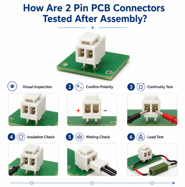
To combat this, an elite manufacturing workflow utilizes a dedicated cross-functional engineering framework. Every project is assigned an experienced account manager paired with a specialized triad of engineers—covering layout optimization, fabrication DFM, and automated assembly diagnostics.

This engineering team carefully manages the entire thermal profile of the epoxy application:

  • Vacuum De-airing: Eliminating microscopic bubbles from potting mixtures prior to dispensing.
  • Precision Pre-Baking: Eliminating moisture from the FR4 substrate to prevent internal delamination.
  • Controlled Cure Ovens: Following strict ramp-up and cool-down temperature curves to minimize structural stress on delicate internal board layers.

Why Partner with EBest for Advanced Circuit Board Epoxy Applications and Turnkey PCBA?

At EBest, we understand that mastering circuit board epoxy chemistry is only the first step toward delivering zero-defect electronics. Achieving true hardware reliability at scale requires an integrated manufacturing partner. Here is how EBest transforms your technical requirements into high-performance, market-ready products:

  • Expert 1+3 Technical Support Model: For every project, you are assigned one dedicated account manager and three specialist engineers (spanning PCB layout, DFM fabrication, and PCBA assembly control) to collaboratively review your files and optimize your epoxy profiles.
  • Automated Selective Precision: Our facility utilizes advanced automated multi-axis robotic dispensing systems, ensuring uniform thickness for circuit board epoxy coating and potting without risking overflow onto critical exclusion zones.
  • Robust IP Defense & Ruggedization: We offer specialized circuit board black epoxy encapsulation and high-temperature (150 ℃) material processing to shield your proprietary layouts from both environmental hazards and reverse-engineering.
  • Seamless Turnkey Execution: From multi-layer FR4 glass epoxy substrate fabrication and precise components sourcing to advanced via filling and final product assembly, we manage your entire production lifecycle under one roof.

Ready to ruggedize your next electronic assembly? A warm welcome to contact EBest anytime via email at sales@bestpcbs.com to upload your BOM and Gerber files, and experience our high-speed, professional turnkey engineering services.

FAQs About Circuit Board Epoxy in PCB Manufacturing

Q1: Can bubbles in epoxy on a circuit board cause problems during assembly?

Yes. Trapped air bubbles create internal voids. Under high voltage, these voids can cause localized corona discharges and high-voltage arcing, leading to insulation breakdown. In high-power modules, air pockets act as thermal barriers, trapping heat and causing components to burn out prematurely.

Q2: Is printed circuit board epoxy fill always conductive?

No. Fabricators utilize both conductive (silver-filled) and non-conductive epoxies. Non-conductive epoxy filling is far more common for standard via-in-pad structures because it matches the thermal expansion properties of the surrounding FR4 laminate more closely, reducing thermal stress fractures.

Q3: How do manufacturers cure conductive epoxy properly?

Conductive and structural epoxies require a precise thermal profile inside automated industrial curing ovens. Technicians carefully control the temperature ramp rate to ensure uniform cross-linking across the entire surface area, preventing internal mechanical stresses that could warp thin multilayer substrates.

Q4: Do you provide standalone electronic repair services for potted boards?

No. As an industrial-grade PCB manufacturing and PCBA processing facility, we do not provide standalone consumer repair services for third-party electronics. We do, however, provide comprehensive engineering rework and design modifications for batch production orders and prototype series handled directly inside our manufacturing facility.

You may also like

High Volume PCB Assembly: Process and Supplier Guide

May 20th, 2026

High volume PCB assembly helps companies build large numbers of assembled circuit boards with stable quality and repeatable results. It is widely used in industrial control, medical devices, automotive electronics, telecom equipment, robotics, LED lighting, and smart hardware. However, mass production is very different from prototype assembly. It needs better planning, stronger process control, stable components, and clear testing standards. Therefore, choosing the right manufacturing partner is important before your product moves into large-scale production.

high volume pcb assembly

What Is High Volume PCB Assembly?

High volume PCB assembly is the process of producing assembled printed circuit boards in large quantities. These boards are also called PCBAs. They include bare PCBs, electronic components, solder joints, and sometimes cables, connectors, coating, or enclosures.

In simple words, this process turns a PCB design into many finished circuit board assemblies. These assemblies are then used in real products, such as power modules, control systems, medical instruments, communication devices, and smart electronics.

Usually, high volume PCB assembly starts after the prototype has passed testing. At this stage, the product design is already stable. As a result, the main goal changes from design checking to stable production.

A typical high volume PCB assembly project may include:

  • PCB fabrication
  • Component sourcing
  • SMT assembly
  • Through-hole assembly
  • AOI inspection
  • X-ray inspection
  • Functional testing
  • Conformal coating
  • Final inspection
  • Packing and shipment

Compared with prototype assembly, high volume production needs more control. For example, the factory must manage solder paste printing, component placement, reflow temperature, test results, material batches, and production records. Also, the same quality level must be repeated across every batch.

Therefore, a good high volume PCB assembly manufacturer should not only assemble boards. It should also review files, check risks, manage components, control quality, and support long-term production.

Types of High Volume PCB Assembly

There are several types of high volume PCB assembly. Each type fits different product designs and application needs. Therefore, the right choice depends on your board structure, component type, testing needs, and final use.
TypeWhat It MeansCommon Use
SMT PCB AssemblyComponents are mounted on the PCB surface.IoT devices, telecom boards, medical electronics
Through-Hole AssemblyComponents with leads are inserted into PCB holes.Power boards, connectors, industrial controls
Mixed AssemblySMT and through-hole parts are used on one board.Automotive modules, control boards, LED drivers
Single-Sided AssemblyComponents are placed on one side of the PCB.Simple electronic products
Double-Sided AssemblyComponents are placed on both sides of the PCB.Compact electronic devices
Box-Build AssemblyPCBA is assembled with housing, cables, labels, and final testing.Finished electronic products
Automated High Volume PCB AssemblyMachines handle printing, placement, soldering, and inspection.Large OEM production

SMT assembly is very common in high volume production. It supports small components, compact layouts, and fast placement. Also, modern SMT machines can place components with high speed and good accuracy.

Through-hole assembly is still useful. Many connectors, relays, transformers, and power parts need stronger mechanical support. Therefore, many industrial and power products still use through-hole components.

Mixed assembly is also common. Many real products use both tiny SMD parts and larger plug-in parts. For example, a control board may include ICs, resistors, capacitors, relays, terminal blocks, and connectors.

Box-build assembly goes one step further. It can include enclosure assembly, cable connection, label application, firmware loading, and final product testing. As a result, customers can receive a more complete product instead of only a bare PCBA.

Benefits of High Volume PCB Assembly Orders

High volume PCB assembly orders bring many practical benefits. These benefits become stronger when the design is stable and demand is clear.

Lower unit cost

  • First, large orders can help reduce the cost per unit. This is because setup costs can be shared across more boards. These costs may include stencil making, engineering review, SMT programming, test fixture preparation, and first article inspection.
  • Also, component purchasing may become more efficient. Larger demand can help improve sourcing plans and reduce repeated purchasing work.

More stable quality

  • Second, high volume production allows the factory to build a stable process. For example, the team can set the solder paste thickness, placement program, reflow profile, AOI rules, and test steps. After that, the same process can be used again and again.
  • As a result, the output becomes more consistent.

Better production speed

  • Third, mass production is easier to plan. Materials can be prepared in advance. SMT feeders can be set before production. Operators can follow clear work instructions. Therefore, the whole production flow becomes smoother.

Stronger quality control

  • Also, high volume orders make quality tracking easier. The factory can review defect data, test results, yield rate, and process issues. This helps improve production step by step.

More reliable supply

  • For OEM companies, stable PCBA supply is very important. If a product is already selling in the market, delayed boards can affect delivery plans. Therefore, high volume PCB assembly helps support regular shipments and market demand.

Better engineering improvement

  • In addition, repeated production can provide useful feedback. The manufacturer may suggest better panel design, alternative components, test point changes, or process improvements. These suggestions can help the next production batch become more efficient.

What Is the High Volume PCB Assembly Process?

The high volume PCB assembly process includes several controlled steps. Each step has a clear purpose. Therefore, the process should start with a full review before mass production begins.

StepMain WorkPurpose
1. File ReviewCheck Gerber, BOM, CPL, drawings, and test needs.Find issues early.
2. DFM ReviewReview design for manufacturing.Improve production success.
3. BOM CheckConfirm part numbers, packages, and alternatives.Keep materials stable.
4. PCB FabricationProduce the bare circuit boards.Build the base of the PCBA.
5. Incoming InspectionCheck PCBs and components.Control material quality.
6. Solder Paste PrintingPrint solder paste on pads.Prepare for SMT mounting.
7. SMT PlacementPlace components by machine.Improve speed and accuracy.
8. Reflow SolderingMelt solder paste to form joints.Create electrical connection.
9. AOI / X-ray InspectionCheck soldering and placement.Find defects early.
10. Through-Hole AssemblyInsert and solder plug-in parts.Add stronger components.
11. TestingRun ICT, functional test, or custom test.Check board performance.
12. Final InspectionCheck appearance, labels, and packing.Prepare for shipment.

The process usually begins with file review. The manufacturer checks Gerber files, BOM, CPL files, assembly drawings, and test instructions. This step is important because small file mistakes can affect a large batch.

Next comes DFM and DFA review. DFM means design for manufacturing. DFA means design for assembly. These reviews help check spacing, footprints, polarity marks, soldering risk, and panel layout.

After that, the factory checks the BOM. This step confirms part numbers, brands, packages, and supply status. Also, the team may suggest approved alternatives if some components are hard to buy.

Then the factory prepares the production line. This includes stencil design, SMT programming, feeder setup, reflow profile setting, and test fixture preparation.

After preparation, assembly begins. The line prints solder paste, places components, and runs the boards through reflow soldering. Then AOI checks missing parts, wrong parts, polarity, bridges, and solder quality.

If the board has BGA, QFN, LGA, or other hidden solder joints, X-ray inspection may be used. After that, through-hole components can be inserted and soldered.

Finally, the boards go through testing, final inspection, packing, and shipment. For many industrial, medical, automotive, and communication products, functional testing is very important. It helps confirm that each board works as expected.

What Is Considered a High Volume PCB Assembly?

There is no fixed number for high volume PCB assembly. The meaning depends on the product type, board complexity, component count, and production plan.

For a simple electronic board, high volume may mean 5,000 pieces or more. For a complex medical, industrial, or telecom board, even 1,000 pieces may be high volume. This is because complex boards need more testing, more process control, and more engineering work.

Here is a simple way to understand the difference:

Project TypeLow VolumeMedium VolumeHigh Volume
Simple PCBA1–500 pcs500–5,000 pcs5,000+ pcs
Complex PCBA1–100 pcs100–1,000 pcs1,000+ pcs
Production PlanOne-time orderSmall repeat ordersRegular production
Design StatusPrototype stagePilot run stageStable product
Process ControlFlexibleSemi-standardHighly repeatable

A project is usually ready for high volume production when:

  • The PCB design has passed testing.
  • The BOM is confirmed.
  • The components are available.
  • The test method is clear.
  • The product demand is stable.
  • The packing method is confirmed.
  • The quality standard is agreed.

However, it is wise to run a pilot batch before full production. A pilot run helps test the process, confirm fixtures, check soldering results, and review functional performance. After that, the full batch can move forward with more confidence.

How Fast Can High Volume Quick Turn PCB Assembly Be Delivered?

High volume quick turn PCB assembly depends on several factors. These include PCB complexity, component supply, order quantity, testing needs, and factory capacity.

For repeat orders, delivery can be faster. This is because the stencil, SMT program, assembly notes, and test method may already be ready. Also, the team already understands the product.

For new projects, more preparation is needed. The factory must review files, confirm materials, build fixtures, prepare the line, and approve the first article. Therefore, new high volume orders usually need more time than repeat orders.

Several factors can affect delivery time.

PCB structure

  • A simple FR4 PCB is usually faster to produce. However, HDI PCB, rigid-flex PCB, heavy copper PCB, Rogers PCB, ceramic PCB, or metal core PCB may need more time.

Component availability

  • Components are often the main factor. If all parts are in stock, production can move faster. However, if some ICs, connectors, or power parts have long lead times, the schedule may become longer.

Testing requirements

  • Basic inspection is faster. However, ICT, functional testing, burn-in, firmware programming, and custom test fixtures need more preparation.

Order quantity

  • Larger orders take more production time. Still, the process can be efficient when materials and equipment are ready.

Communication speed

  • Fast replies help shorten the schedule. For example, the customer may need to approve component alternatives, first articles, or engineering questions.

Therefore, a one-stop supplier can often support faster delivery. When PCB fabrication, component sourcing, assembly, and testing are handled together, the project becomes easier to manage.

What Do High Volume PCB Assembly Services Usually Include?

High volume PCB assembly services should cover more than basic soldering. A strong supplier should support the full production chain. This helps reduce communication work and improves project control.

Common services include the following:

PCB fabrication

  • The supplier produces bare PCBs according to Gerber files and technical requirements. These may include board material, layer count, copper thickness, solder mask, surface finish, impedance control, and special process needs.

Component sourcing

  • The supplier helps buy original components from reliable channels. Also, the team can review the BOM and check part availability. If needed, they may suggest alternatives for engineering approval.

SMT assembly

  • SMT assembly includes solder paste printing, component placement, reflow soldering, and AOI inspection. For high volume orders, this step must be fast and stable.

Through-hole assembly

  • Some products need plug-in parts, such as connectors, relays, transformers, terminal blocks, and switches. Therefore, the supplier may use wave soldering, selective soldering, or manual soldering.

Inspection and testing

  • Testing may include AOI, X-ray, flying probe, ICT, functional testing, aging test, and custom test fixtures. The right method depends on the product and application.

Conformal coating

  • Some products work in humid, dusty, or harsh environments. In this case, conformal coating can help protect the PCBA surface.

Box-build assembly

  • Box-build assembly includes PCBA installation, enclosure assembly, cable connection, labeling, firmware loading, final testing, and packaging. As a result, customers can receive a more complete product.

Traceability and records

  • Traceability is very useful in high volume production. It helps track material batches, production steps, inspection results, and shipment records. This is especially important for medical, automotive, industrial, and aerospace-related products.

How Do You Choose a High Volume PCB Assembly Manufacturer?

Choosing a high volume PCB assembly manufacturer should be done carefully. The right partner can help improve quality, delivery, cost control, and long-term production stability.

Here are the main points to check.

Manufacturing capability

  • First, check whether the supplier can build your PCB type. Some projects may need multilayer PCB, HDI PCB, rigid-flex PCB, heavy copper PCB, ceramic PCB, RF PCB, or metal core PCB. Also, the factory should support your component packages, such as BGA, QFN, fine-pitch ICs, and small passive parts.

Engineering support

  • Next, review the supplier’s engineering support. A good team can provide DFM review, BOM checking, panel suggestions, process advice, and test planning. This support helps reduce issues before mass production.

Supply chain ability

  • Component supply is very important. Therefore, the supplier should have reliable sourcing channels, incoming inspection, and alternative part support.

Quality system

  • Also, check the quality system. The factory should have clear inspection steps, production records, test methods, and traceability. For regulated industries, this is even more important.

Testing capability

  • Different products need different tests. Some only need AOI and basic electrical testing. Others need functional testing, firmware loading, burn-in, or custom fixtures. So, the supplier should understand your product testing needs.

Production planning

  • High volume projects need good planning. The factory should manage material arrival, line capacity, production schedule, inspection time, and shipping date.

Communication

  • Finally, clear communication matters. A responsive team can answer questions, confirm details, and solve issues quickly. This is helpful during both new production and repeat orders.

Before choosing a supplier, you can ask:

  • Can you support PCB fabrication and PCBA assembly together?
  • Can you provide turnkey component sourcing?
  • Do you offer DFM and BOM review?
  • What inspection methods do you use?
  • Can you support functional testing?
  • How do you manage traceability?
  • What industries have you served?
  • Can you support repeat production?

These questions can help you find a supplier that fits your product and long-term needs.

Why Should You Choose EBest Circuit (Best Technology) as Your Preferred Partner?

EBest Circuit (Best Technology) supports customers from PCB fabrication to PCBA assembly, component sourcing, testing, and turnkey electronics manufacturing. Therefore, customers can manage complex projects with one experienced team.

One-stop PCB and PCBA support

  • EBest Circuit provides PCB fabrication, SMT assembly, through-hole assembly, component sourcing, testing, and box-build assembly. This helps reduce vendor coordination and keeps the project easier to control.
DFM review before production

  • Before assembly, the engineering team can review Gerber files, BOM, CPL files, drawings, and test requirements. Also, they can check soldering risks, spacing issues, footprint concerns, panel design, and polarity marks.

Wide PCB technology coverage

  • EBest Circuit supports many PCB types, such as FR4 PCB, high-Tg PCB, metal core PCB, ceramic PCB, Rogers high-frequency PCB, heavy copper PCB, rigid-flex PCB, and multilayer PCB. As a result, customers can use one supplier for different board needs.

Component sourcing support

  • High volume production needs stable materials. EBest Circuit can support component sourcing, BOM review, and alternative part suggestions. This helps customers save time and reduce sourcing pressure.

Inspection and testing

  • The company supports quality checks such as AOI, X-ray inspection, electrical testing, and functional testing based on project needs. These steps help keep production stable and reliable.

Experience in demanding industries

  • EBest Circuit supports demanding industries such as medical devices, industrial control, automotive electronics, aerospace/UAV, communications, robotics, new energy, and LED lighting. These applications require stable production, strict process control, and reliable long-term performance. To support these requirements, we operate under a comprehensive quality management system with certifications such as ISO 9001, ISO 13485, IATF 16949, AS9100D, and UL recognition. Therefore, customers can rely on us for projects that need controlled manufacturing, clear documentation, material traceability, and consistent PCBA quality from prototype to high volume production.

Traceability and production records

  • For high volume PCB assembly, traceability is important. EBest Circuit can support material tracking, production records, inspection records, and shipment control. This helps customers manage repeat orders and quality follow-up.

Support from prototype to mass production

  • Many projects begin with prototypes. Then they move to pilot runs and mass production. EBest Circuit can support each stage. Therefore, customers can move from design validation to high volume production more smoothly.

If you need a reliable high volume PCB assembly manufacturer, EBest Circuit (Best Technology) can help review your files and provide a suitable quotation. Please send your Gerber files, BOM, CPL file, assembly drawing, quantity, and testing requirements to sales@bestpcbs.com.

FAQs About High Volume PCB Assembly

Q1: What files are needed for a high volume PCB assembly quote?
A1: You usually need Gerber files, BOM, CPL file, assembly drawing, PCB specifications, testing requirements, and order quantity. If you need turnkey service, the BOM should include part numbers, packages, and approved alternatives if available.

Q2: Should I make a prototype before high volume PCB assembly?
A2: Yes. A prototype or pilot batch helps check the design, components, soldering quality, and test method before mass production. As a result, the full production run becomes more stable.

Q3: Can high volume PCB assembly include component sourcing?
A3: Yes. Many customers choose turnkey service. In this model, the supplier handles PCB fabrication, component sourcing, assembly, inspection, and testing.

Q4: What affects the cost of high volume PCB assembly?
A4: The main cost factors include PCB type, board size, layer count, component quantity, component package, testing needs, coating needs, packing method, and delivery schedule.

Q5: How can I improve the yield of a high volume PCBA order?
A5: Start with DFM and DFA review. Also, use clear footprints, stable components, proper panel design, enough test points, and clear test steps. A pilot run is also helpful.

Q6: What is the difference between high volume and low volume PCB assembly?
A6: Low volume assembly is often used for prototypes or small batches. High volume assembly is used for stable products that need regular production. Therefore, high volume projects need more process control and planning.

Q7: Can high volume quick turn PCB assembly be done for urgent orders?
A7: Yes, in many cases. However, delivery depends on PCB complexity, component availability, testing needs, and production capacity. Repeat orders are usually faster than new projects.

Q8: What industries use high volume PCB assembly services?
A8: It is widely used in industrial control, medical devices, automotive electronics, telecom equipment, robotics, IoT devices, new energy systems, LED lighting, and smart hardware.

Q9: Why is testing important in high volume PCB assembly?
A9: Testing helps confirm that each board works as expected. Also, it helps find issues before shipment. This is very important when many boards are produced in one batch.

Q10: How do I start a project with EBest Circuit?
A10: You can send your Gerber files, BOM, CPL file, assembly drawing, quantity, and testing needs to sales@bestpcbs.com. The team will review your project and provide quotation support.

You may also like

What is mSAP PCB Technology? SAP vs mSAP

May 19th, 2026

Are you troubled by traditional PCB fabrication limitations when developing smaller, denser, and faster electronic products? mSAP PCB Technology is the solution to these core pain points. Traditional etching cannot meet the demand for ultra-fine line widths and tight spacing, especially in the era of high-speed electronics where standard processes fall short. As a modified semi-additive process, mSAP achieves finer, more precise traces through selective copper plating, adapting well to advanced HDI and substrate-like PCBs. Read on to learn how mSAP can solve your PCB manufacturing challenges and unlock new design possibilities.

mSAP PCB Technology, https://www.bestpcbs.com/blog/2026/05/msap-pcb-technology/

What is mSAP PCB Technology?

At its core, mSAP PCB technology officially the Modified Semi-Additive Process is a method for creating fine-line circuits in advanced PCB manufacturing. Unlike traditional subtractive processes, which start with a thick copper layer and etch away what’s not needed, mSAP begins with an extremely thin copper layer and selectively plates additional copper exactly where traces are required. This approach results in far finer, more precise circuit patterns, making it ideal for designs that demand small line widths, tight spacing, dense BGA escape routing, or shorter signal paths.

One of the pain points with traditional subtractive processes is that narrow traces are prone to copper undercut, which degrades sidewall quality. mSAP avoids this by focusing on building up copper rather than removing it, resulting in more vertical, tightly controlled trace profiles. From a technical standpoint, mSAP sits right between conventional HDI PCB fabrication and the more advanced SAP (Semi-Additive Process) or IC substrate processes it gives designers greater routing freedom while remaining far more practical for standard PCB production than full SAP.

What Are Advantages of mSAP PCB Technology?

mSAP really shines in advanced PCB manufacturing, especially for designs that need to pack a lot of routing into a small space. Here are its advantages:

  • Finer Line and Space: Unlike conventional etching, mSAP supports much smaller line widths and spacing, letting you fit more traces into narrow routing channels.
  • Higher Routing Density: With finer traces and tighter spacing, you can route more signals in the same board area either reducing the overall size of the PCB or adding more functionality without increasing its footprint.
  • Better BGA Escape Routing: Fine-pitch BGA packages often require tight routing channels, and mSAP makes it easier to create more routing paths between pads critical for advanced processors, communication chips, and high-density modules.
  • Cleaner Trace Geometry: Since mSAP relies on selective copper plating rather than heavy etching, trace sidewalls are more vertical, leading to more predictable electrical behavior.
  • Improved Impedance Control: Stable trace geometry is key for controlled impedance designs, which are essential for high-speed digital signals, RF circuits, and communication boards.
  • Shorter Signal Paths: Higher routing density means fewer long detours for signals, improving signal timing and overall layout efficiency.
  • Support for Miniaturized Electronics: If you’re working on compact devices, wearables, 5G modules, or advanced HDI structures, mSAP is an excellent choice it’s built for small, high-performance PCBs.
  • Better PCB Area Utilization: You can fit more functionality into the same board space, which is crucial for products where size, weight, and layout efficiency are top priorities.

    What Are the Limitations of mSAP PCB Technology?

    While mSAP is powerful, it’s not a one-size-fits-all solution. Here are its main limitations to keep in mind:

    • Higher Manufacturing Cost: mSAP requires advanced imaging, plating, and inspection equipment, so it’s usually more expensive than standard subtractive PCB fabrication.
    • Demanding Process Control: Fine-line production is sensitive to small variations even minor changes in exposure, plating, or flash etching can affect trace quality. This means you need stable equipment and precise process windows.
    • Strict DFM Review: Before production, you’ll need to carefully review the layout, stackup, line/space, copper thickness, via structure, and impedance targets DFM (Design for Manufacturability) is even more critical with mSAP.
    • Material Dependence: The substrate you use needs to support fine-line imaging, dimensional stability, and microvia reliability not all standard PCB materials are suitable for mSAP.
    • Unnecessary for Standard Designs: For normal multilayer PCBs, power boards, or simple control boards, subtractive etching is still more efficient and cost-friendly. There’s no need to use mSAP if your design doesn’t require its fine-line capabilities.

      What Are Applications of mSAP Technology?

      mSAP is most useful in products where space is limited and circuit density is high. Here are some of its most common applications:

      • Smartphones and Mobile Devices: These devices need compact boards with dense routing, fine-pitch components, and thin structures all areas where mSAP excels.
      • Wearable Electronics: Wearables require small, lightweight, highly integrated PCBs, and mSAP helps fit more functions into a tiny space.
      • 5G Communication Modules: 5G products need high-frequency performance, controlled impedance, compact layouts, and reliable signal paths mSAP delivers all of these.
      • Advanced HDI PCBs: If your HDI design requires fine line/space, microvias, or high routing density, mSAP is the perfect match.
      • Substrate-Like PCBs: These structures sit between conventional PCBs and IC substrates, and mSAP is well-suited to their unique requirements.
      • Medical Electronics: Portable medical devices, monitoring equipment, and compact diagnostic modules often need reliable, dense interconnection mSAP fits the bill.
      • Automotive Electronics: ADAS modules, sensors, control units, and high-speed automotive electronics often require fine routing and stable signal integrity mSAP delivers both.
      • High-Speed Computing Modules: Advanced processors, memory modules, and high-speed interface boards benefit from mSAP’s shorter signal paths and tighter impedance control.

      What Are Technical Parameters of mSAP PCB Technology?

      The real value of mSAP lies in its tightly controlled parameters, all of which work together to enable its fine-line capabilities. Below is a detailed table of the technical parameters of mSAP PCB technology:

      Technical ParameterTypical Range/Standard
      Line Width20–60 μm (can reach 10–20 μm for advanced products)
      Line Spacing20–60 μm (can reach 10–20 μm for advanced products)
      Starting Copper ThicknessExtremely thin (typically a few micrometers)
      Final Copper ThicknessDepends on design requirements, usually 10–50 μm
      Trace Sidewall ShapeClean, vertical (minimal undercut)
      Registration AccuracyHigh precision (typically ±5 μm or better)
      Mask AlignmentConsistent with registration accuracy
      Microvia CapabilityCompatible with microvia formation (diameter down to 50 μm)
      Impedance ControlTight control (±5% tolerance typical)
      Inspection & TestingAOI, electrical testing, cross-section analysis
      mSAP PCB Technology, https://www.bestpcbs.com/blog/2026/05/msap-pcb-technology/

      What is the Process of mSAP PCB?

      The mSAP PCB process blends imaging, selective plating, and light etching, leaning more toward additive manufacturing but still including a controlled etching step to remove the thin seed copper layer. Here’s a step-by-step breakdown of how it typically works:

      1. Base Material Preparation: We start with a dielectric material coated with an extremely thin copper layer one that’s suitable for fine-line imaging and microvia formation.

      2. Surface Cleaning and Treatment: The copper surface is thoroughly cleaned and treated to improve adhesion, which is essential for ensuring consistent results in the subsequent plating and imaging steps.

      3. Photoresist Coating: A layer of photoresist is applied to the copper surface; this layer will define exactly where copper will be plated and where it won’t.

      4. Imaging and Exposure: The circuit pattern is transferred onto the photoresist via exposure, a step that requires precise mask positioning to avoid any pattern shifts even small misalignments can ruin fine-line circuits.

      5. Development: The unwanted portions of the photoresist are removed, leaving open areas where copper will be plated.

      6. Selective Copper Plating: Copper is plated only in the exposed circuit pattern areas this is the heart of mSAP’s fine-line advantage, as it allows for precise control over trace shape and size.

      7. Photoresist Stripping: Any remaining photoresist is stripped away, leaving behind the newly plated copper traces.

      8. Flash Etching: The thin seed copper layer between the traces is lightly etched away this is a gentle process, far easier to control than the heavy etching used in subtractive processes.

      9. Inspection and Testing: AOI, electrical testing, and cross-section analysis are used to verify that the circuit meets all design requirements and quality standards.

        To put it simply: subtractive etching forms traces by removing copper, while mSAP forms traces by adding copper selectively and only removing the thin seed layer resulting in cleaner, more precise circuits.

        mSAP PCB Process, https://www.bestpcbs.com/blog/2026/05/msap-pcb-technology/

        What is the Difference between SAP and mSAP?

        While both SAP and mSAP fall under the semi-additive process family, they differ in several ways that make them suitable for different applications. Here’s a clear breakdown:

        ItemSAPmSAP
        Full NameSemi-Additive ProcessModified Semi-Additive Process
        Starting Copper LayerExtremely thin seed copperThin copper layer (more PCB-production friendly)
        Circuit FormationCopper added to form traces (minimal starting copper)Selective plating, then flash etching of seed layer
        Line/Space CapabilityFiner (closer to IC substrate-level)Fine-line (for advanced HDI and substrate-like PCBs)
        Main ApplicationIC substrates, ultra-fine circuits, advanced packagingHDI PCB, compact electronics, substrate-like PCB
        Process ComplexityHigherHigh (but more adaptable to PCB manufacturing)
        CostGenerally higherMore practical for advanced PCB projects
        SAP and mSAP, https://www.bestpcbs.com/blog/2026/05/msap-pcb-technology/

        SAP is capable of extremely fine features, but it requires highly advanced process control. For most designs that need fine-line performance without the complexity of full SAP, mSAP is the preferred choice it’s far more aligned with standard PCB production methods while still delivering the necessary precision.

        What is the Difference between Subtractive and mSAP?

        The biggest difference between subtractive processes and mSAP boils down to how copper circuit patterns are created. Here’s a straightforward comparison to help you understand which is right for your project:

        ItemSubtractive ProcessmSAP Process
        Basic PrincipleRemoves unwanted copperAdds copper where traces are needed
        Starting CopperThicker copper foilVery thin copper layer
        Trace FormationMainly through etchingMainly through selective plating
        Fine-Line ControlDifficult for small tracesIdeal for fine-line patterns
        Trace SidewallProne to etching undercutCleaner, more vertical profile
        Best UseStandard PCB, common multilayer PCB, normal HDIAdvanced HDI, fine-line PCB, substrate-like PCB
        CostMore cost-effective for normal designsHigher (but valuable for dense designs)

        Subtractive etching is still the go-to for standard PCBs it’s mature, reliable, and cost-effective. But when your design demands finer geometry, higher density, or tighter electrical control, mSAP is the clear upgrade.

        Future Trends of mSAP PCB Technology

        The future of mSAP is closely tied to the ongoing trends of miniaturization, high-speed electronics, and advanced packaging. Here’s what we can expect in the coming years:

        • Growth of Substrate-Like PCB: As electronic products get thinner and more integrated, substrate-like PCBs will become more common and mSAP is perfectly positioned to support their fine-line and dense interconnection needs.
        • More Demand from High-Speed and RF Designs: High-speed signals require tighter impedance control and more predictable trace geometry, and mSAP will become increasingly essential for these designs, especially as signal speeds continue to rise.
        • Closer Connection Between PCB and Packaging: The line between PCB manufacturing and semiconductor packaging is getting blurrier, and mSAP (along with advanced HDI, SLP, and SAP) will play a key role in this integration.
        • Improved Imaging and Registration Technology: Better direct imaging, exposure systems, and registration control will make mSAP more reliable, boosting yields and enabling even finer line/space capabilities.
        • More Use in Compact Industrial and Medical Devices: mSAP will move beyond consumer electronics (like smartphones and wearables) and into more specialized, high-reliability applications, such as industrial sensors and medical devices.
        • Stronger DFM Collaboration: Successful mSAP projects will require closer collaboration between product designers, PCB manufacturers, and assembly teams. Early DFM reviews will become even more important to reduce layout risk and ensure production success.

          FAQs About mSAP PCB Technology

          Q1: What is mSAP PCB Technology and how does it differ from traditional PCB manufacturing processes?

          A1: mSAP (Modified Semi-Additive Process) is an advanced PCB manufacturing method designed to create fine-line circuits. Unlike traditional subtractive processes that etch away excess copper, mSAP starts with an extremely thin copper layer and selectively plates additional copper to form traces, then uses gentle flash etching to remove the remaining seed layer. This approach avoids copper undercut and achieves finer, more precise traces, making it ideal for high-density, miniaturized designs where traditional processes fall short.

          Q2: What line width and spacing can mSAP PCB Technology typically achieve?

          A2: The typical line width and spacing range for mSAP is 20–60 μm, and advanced mSAP processes can reach 10–20 μm. This is significantly finer than the capabilities of conventional subtractive etching, enabling higher routing density and more compact PCB designs for advanced electronic products.

          Q3: How does mSAP compare to SAP (Semi-Additive Process) in terms of practicality and cost?

          A3: Both are semi-additive processes, but SAP uses an extremely thin seed layer to achieve ultra-fine features (closer to IC substrate-level) with higher complexity and cost. mSAP is a modified, more practical version that balances performance and manufacturability, it supports fine-line routing but is more adaptable to standard PCB production, making it a more cost-effective choice for most advanced PCB projects.

          Q5: What are the main limitations of mSAP PCB Technology that designers should consider?

          A5: The primary limitations of mSAP include higher manufacturing costs (due to advanced equipment requirements), strict process control needs (small variations can affect trace quality), reliance on suitable substrate materials, and the need for rigorous DFM (Design for Manufacturability) reviews. Additionally, mSAP is unnecessary for standard PCB designs where traditional subtractive processes are more efficient and cost-friendly.

          Q6: Does mSAP PCB Technology support impedance control, and why is this important?

          A6: Yes, mSAP supports tight impedance control (typically ±5% tolerance) thanks to its ability to create clean, vertical trace sidewalls and precise trace geometry. This is critical for high-speed digital signals, RF circuits, and 5G modules, as stable impedance ensures reliable signal transmission and reduces interference.

          Q7: What are mSAP PCB technology position masks and how do they affect the quality of mSAP PCBs?

          A7: mSAP PCB technology position masks refer to the precise alignment and positioning of photoresist masks during the imaging and exposure stages of mSAP PCB manufacturing. They cover key aspects including mask positioning accuracy, photoresist alignment, exposure precision, and registration control. These masks directly affect mSAP PCB quality because even tiny deviations (a few micrometers) can lead to short circuits, inconsistent trace widths, or signal integrity issues that damage fine-line circuits.

          Conclusion

          mSAP PCB technology gives designers and manufacturers a practical way to build finer, denser, and more controlled circuit structures filling the gap where standard subtractive etching can no longer deliver. When comparing SAP vs mSAP, SAP offers finer capabilities but at the cost of greater complexity and expense. mSAP, on the other hand, strikes a balance between performance and practicality, making it ideal for advanced PCB production.

          Subtractive processing still has its place for standard boards, but mSAP is invaluable for designs that demand fine-line HDI, compact electronics, or substrate-like PCBs. If your project requires high routing density, fine-pitch BGA escape, controlled impedance, or a smaller board size, mSAP is the technical advantage you need to bring your design to life.

          You may also like

          Telecom Board: How to Build Reliable Telecommunications Circuit Boards

          May 19th, 2026

          A telecom board supports signal transfer, power control, data exchange, and network communication inside telecom equipment. It may look like a common PCB, but it often needs tighter control over layout, materials, impedance, assembly, and testing. Therefore, engineers and buyers should understand how each manufacturing step affects final performance. In this guide, we explain what a telecom board is, where it works, what layout details matter, how manufacturers build it, and how EBest Circuit supports telecom PCB fabrication and assembly from prototype to production.

          telecom board

          What Is a Telecom Board?

          A telecom board is a printed circuit board for communication equipment. People may also call it a telecommunications board, telecom PCB, or telecom circuit board.

          In simple terms, this board helps electronic devices send, receive, process, or control communication signals. These signals may come from RF modules, optical devices, routers, switches, gateways, or wireless systems.

          Unlike a simple control board, a telecom board often needs better signal control. For example, it may need controlled impedance, stable grounding, low signal loss, clean power delivery, or high-speed data routing. Also, many telecom products run for long hours. So, the board must support stable operation over time.

          A telecom board can use different structures. It may be a standard FR4 PCB, a high-frequency PCB, a multilayer PCB, a rigid-flex PCB, or a metal core PCB. The right choice depends on the product design, working frequency, heat level, size, and assembly needs.

          In real production, a good telecom board does not depend on one factor alone. Instead, it comes from a full process. Layout review, material selection, stack-up control, PCB fabrication, component sourcing, SMT assembly, inspection, and testing all matter.

          ItemWhat It Means for a Telecom Board
          Signal transmissionThe board must support clean and stable signal paths.
          Power controlThe board must deliver steady power to ICs, RF parts, and modules.
          Material choiceThe laminate must match frequency, loss, heat, and cost needs.
          Assembly qualityComponents must be placed and soldered with good process control.
          TestingElectrical, impedance, AOI, X-ray, and functional tests help confirm quality.

          Telecom Board vs Telecommunications Board: Are They the Same?

          In most PCB manufacturing contexts, telecom board and telecommunications board mean nearly the same thing. Both refer to circuit boards for communication products.

          However, the word “board” can create confusion. In some searches, a telecom board may mean a cable installation backer board. In other searches, it may mean a company board of directors or a telecom job board. Because of this, a PCB article should make the meaning clear from the beginning.

          In this article, a telecom board means a PCB or PCBA for electronic communication equipment.

          TermCommon MeaningIn This Article
          Telecom boardA short term with several possible meaningsA PCB or PCBA used in telecom equipment
          Telecommunications boardA more formal termA circuit board for communication systems
          Telecom PCBA clear manufacturing termA bare printed circuit board for telecom use
          Telecom PCBAAn assembled boardA telecom PCB with components mounted on it

          The shorter term telecom board sounds more common and easier to search. The term telecommunications board sounds more formal. Still, both can describe the same product type when we talk about PCB manufacturing.

          For buyers, the name matters less than the actual requirement. A real telecommunications board must support stable signal paths, reliable solder joints, suitable materials, and repeatable production quality. Therefore, the focus should stay on engineering and manufacturing details.

          What Are Telecom Circuit Boards Used For?

          Telecom circuit boards work in many communication systems. Some boards process high-speed digital signals. Some handle RF signals. Others manage power, interfaces, control logic, or network connections.

          ApplicationCommon Board FunctionTypical PCB Requirement
          5G and wireless equipmentSignal transmission, antenna control, RF processingControlled impedance, low-loss material, stable copper geometry
          Routers and switchesData routing, interface control, power regulationMultilayer PCB, BGA assembly, high-speed routing
          Optical communication devicesSignal conversion and data transferCompact layout, stable soldering, fine-pitch assembly
          Industrial gatewaysMachine communication and data exchangeReliable connectors, power control, functional testing
          RF and microwave modulesWireless signal amplification or filteringHigh-frequency laminate, RF trace control, grounding
          IoT communication productsWireless connection and sensor communicationSmall size, stable assembly, cost control

          For example, 5G modules, antenna systems, repeaters, base station parts, and wireless transmission devices often need telecom circuit boards. These boards may require controlled impedance, low-loss materials, and stable copper patterns.

          Routers and switches also need telecom boards. These boards support data transfer, power regulation, interface control, and signal processing. Also, they often include BGA chips, Ethernet interfaces, fine-pitch components, and high-speed signal lines.

          In industrial communication, gateway boards connect machines, sensors, PLCs, and cloud systems. Therefore, their boards often combine communication interfaces, power circuits, isolation areas, and control units.

          As a result, telecom circuit boards cover a wide range of products. However, they share one common goal: they must help communication signals move with stability and low interference.

          What Telecom PCB Layout Factors Affect Signal Integrity?

          Telecom PCB layout has a strong effect on signal quality. EBest Circuit does not position itself as a full circuit design company. However, we can support layout review, DFM suggestions, stack-up review, impedance coordination, and manufacturability checks.

          Before production, engineers should check several layout details.

          Layout FactorWhy It MattersWhat to Review Before Production
          Controlled impedance routingIt helps reduce signal reflection.Trace width, spacing, copper thickness, dielectric thickness
          Differential pair controlIt supports balanced high-speed transmission.Pair spacing, length matching, routing symmetry
          Ground plane continuityIt gives signals a stable return path.Split planes, via stitching, reference layer design
          RF trace clearanceIt reduces noise and coupling.Distance from power, clock, and digital lines
          Via placementIt can affect RF and high-speed signals.Via count, via position, via type, stub length
          Power layoutIt supports stable IC operation.Decoupling placement, power plane design
          Assembly clearanceIt reduces SMT risk.Component spacing, pad size, solder mask clearance

          Many telecom boards need controlled impedance. This is common in RF lines, Ethernet lines, differential pairs, and high-speed digital interfaces. Trace width, spacing, copper thickness, dielectric thickness, and material type all affect impedance. Therefore, the layout and stack-up should match each other.

          Grounding also deserves attention. A clean return path helps signals move with less noise. If a signal crosses a split ground plane, the return path may become unstable. So, ground plane continuity should be checked early.

          RF traces need enough distance from noisy power lines, clock signals, and digital circuits. In many telecom PCBs, engineers also use via fences, shielding areas, or grounded copper to improve isolation.

          A layout may look perfect in design software. However, real PCB production has tolerances. Etching, drilling, plating, solder mask registration, and lamination can all change final results. Therefore, DFM review helps reduce risk before fabrication.

          At EBest Circuit, our layout-related support focuses on practical production checks. We help customers review manufacturability, stack-up feasibility, impedance needs, soldering risks, and assembly clearance.

          telecom board

          How Do Telecom Board Manufacturing Processes Support Stable Signal Transmission?

          Telecom board performance does not come from layout alone. The manufacturing process also plays a major role. Even small process changes can affect impedance, signal loss, solderability, and long-term stability.

          Manufacturing ProcessWhat EBest ControlsHow It Supports Telecom Board Performance
          Stack-up controlLayer order, dielectric thickness, copper thicknessSupports impedance and signal stability
          Imaging and etchingTrace width and spacingHelps keep signal traces close to design targets
          Copper platingHole copper and surface copperSupports via reliability and current flow
          DrillingHole position and hole qualitySupports layer connection and dense routing
          LaminationPressure, temperature, resin flowHelps maintain board flatness and layer bonding
          Surface finishENIG, OSP, HASL, immersion silver, etc.Supports solderability and assembly quality
          Electrical testingCircuit continuityConfirms open and short testing before shipment
          Impedance testingActual impedance valueHelps verify high-speed and RF requirements

          The stack-up defines layer order, dielectric thickness, copper thickness, and reference planes. For controlled impedance boards, stack-up control is very important. EBest can review the stack-up and match it with material and impedance needs.

          Signal traces must stay close to the design target. If etching changes the trace width too much, impedance may shift. Therefore, manufacturers need stable imaging and etching control.

          Vias also matter. Multilayer telecom boards often include many vias. Accurate drilling helps keep layer connections stable. Also, good hole wall preparation supports reliable copper plating.

          Surface finish selection affects assembly quality. Telecom boards may use ENIG, OSP, immersion silver, HASL, or other finishes. ENIG often works well for fine-pitch components and BGA assembly. However, the best finish depends on the product, storage needs, and assembly process.
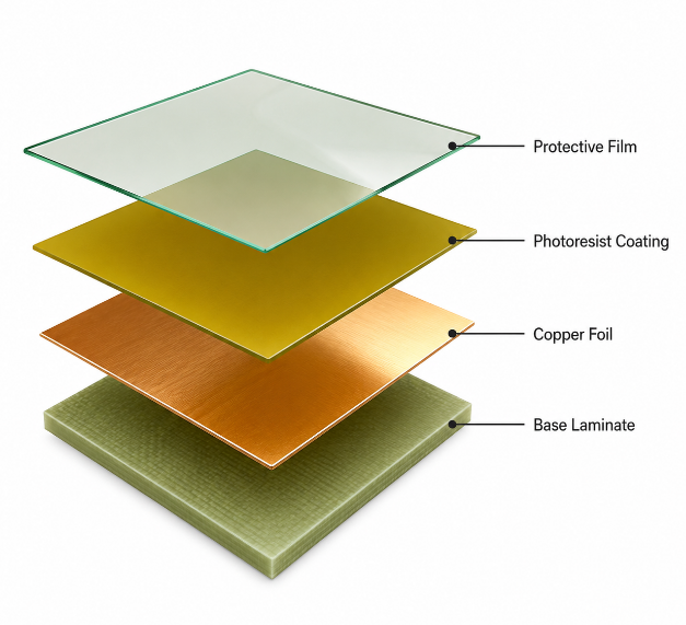
          In short, stable telecom board manufacturing needs tight process control. Each step should support the electrical goal of the board.

          What Materials Are Best for High-Frequency Telecom Circuit Boards?

          Material choice has a direct effect on telecom board performance. Different products need different materials. Therefore, engineers should not choose a material only by price or habit.

          Material TypeBest-Fit Telecom ApplicationMain Advantage
          Standard FR4Control boards, network boards, low-to-mid frequency boardsMature process and cost control
          High-Tg FR4Multilayer boards and higher-temperature productsBetter thermal stability
          Rogers materialRF, microwave, antenna, and high-frequency boardsLower loss and stable dielectric behavior
          PTFE-based laminateLow-loss RF and microwave boardsGood high-frequency performance
          Metal core PCBPower modules and heat-generating telecom boardsBetter heat spreading
          Hybrid stack-upBoards with both RF and digital sectionsBalance between cost and performance

          FR4 works well for many standard telecom control boards, digital boards, and network interface boards. It offers good cost control, easy sourcing, and mature processing.

          High-Tg FR4 supports better thermal stability than standard FR4. It suits multilayer telecom boards, dense assemblies, and products with higher working temperatures.

          Rogers laminates are common in RF, antenna, microwave, and high-frequency telecom PCBs. These materials offer more stable dielectric performance and lower signal loss than standard FR4 in many high-frequency designs.

          Some RF and microwave boards use PTFE-based materials. These materials can support low-loss signal transmission. However, they need careful fabrication control because they behave differently from FR4.

          Some telecom modules generate more heat. For example, power modules or RF amplifier boards may need better thermal paths. In these cases, aluminum or copper base PCBs can help spread heat.

          Also, some telecom boards combine FR4 and high-frequency materials. This can reduce cost while keeping RF layers stable. As a result, hybrid stack-ups often work well when only part of the board needs high-frequency performance.

          When choosing materials, engineers should review dielectric constant, dissipation factor, copper foil type, Tg, CTE, thermal conductivity, thickness tolerance, and supply stability.

          How Does Custom Telecom PCB Assembly Work at EBest?

          Telecom PCB assembly at EBest follows a controlled process from files to finished PCBA. This section does not only talk about “reliability.” Instead, it shows the actual assembly flow and process capability.

          EBest supports telecom PCB assembly for RF modules, communication control boards, network gateway boards, and other telecom-related products.

          Assembly StepWhat EBest DoesCustomer Benefit
          BOM reviewChecks part availability, package, lead time, and alternativesHelps reduce sourcing risk
          DFM reviewChecks pad size, spacing, polarity, stencil needs, and panelizationHelps reduce SMT issues
          Stencil controlMatches stencil design with component packagesImproves solder paste printing
          SMT placementControls component position and directionSupports stable assembly quality
          Reflow controlMatches temperature profile with board and componentsHelps form stable solder joints
          BGA/QFN assemblyHandles hidden and fine-pitch packagesSupports dense telecom PCBAs
          AOI inspectionChecks visible solder joints and placementFinds common assembly defects
          X-ray inspectionChecks hidden solder joints under BGA/QFNImproves inspection confidence
          Functional testingFollows customer test requirementsHelps verify board operation

          First, EBest reviews the BOM and checks component availability. This step helps customers find supply risks early. Also, it helps confirm package type, part lifecycle, lead time, and possible alternatives.

          Next, our team checks assembly-related details. These include pad size, component spacing, solder mask clearance, stencil needs, polarity marks, panelization, and connector placement. As a result, customers can reduce SMT risks before production.

          Telecom boards may include QFN, BGA, small passive parts, RF connectors, and shielding parts. Therefore, stencil design and solder paste control matter. Good solder paste printing helps improve solder joint consistency.

          During SMT placement, EBest controls component position, feeder setup, package direction, and program accuracy. Then, the reflow profile must match the board and component mix. A proper profile helps form stable solder joints and reduces soldering defects.

          Finally, AOI and X-ray inspection help confirm assembly quality. AOI checks visible solder joints, missing parts, polarity, and alignment. X-ray inspection checks hidden solder joints under BGA and QFN packages.

          Through this process, EBest helps customers move from bare telecom PCB to assembled PCBA with fewer handoff issues.

          Telecom Board Manufacturing Across Communication Applications – EBest Case Studies

          EBest Circuit supports telecom board projects across different communication applications. The examples below show how manufacturing choices can support real product needs.

          EBest Project TypeMain ChallengeEBest Support
          RF communication module boardSignal loss and impedance controlStack-up review, high-frequency material support, impedance testing
          Industrial network gateway PCBADense assembly and stable interfacesMultilayer PCB, component sourcing, SMT assembly, AOI, X-ray
          Communication control boardStable operation inside equipmentDFM review, prototype support, assembly, testing
          High-power communication module boardHeat and current handlingCopper thickness review, thermal via feedback, material suggestions

          RF Communication Module Board
          An RF communication module board often needs controlled impedance, stable material performance, and accurate trace control. For this type of board, EBest focuses on stack-up review, high-frequency material handling, copper thickness control, and impedance testing.

          For example, a customer may need an RF board for wireless signal transmission. In this case, material choice and trace accuracy matter. So, EBest reviews the stack-up, confirms the laminate, controls line width, and checks impedance. This helps the board meet the expected signal target.

          Industrial Network Gateway PCBA
          An industrial network gateway often includes processors, memory, power circuits, communication interfaces, connectors, and I/O terminals. Therefore, this project needs both PCB fabrication and PCBA assembly.
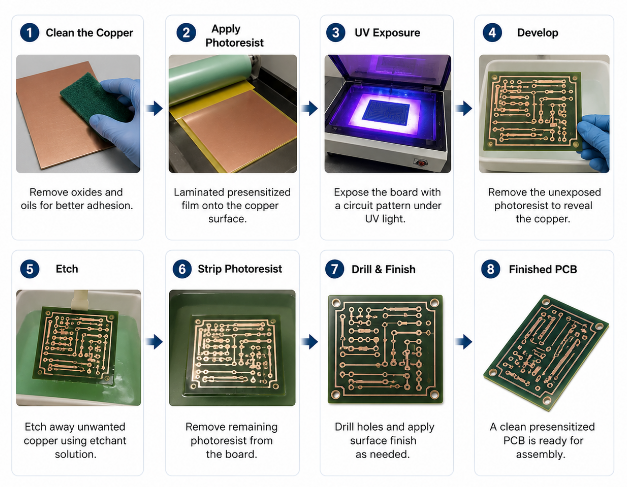
          For this type of board, EBest can support multilayer PCB production, component sourcing, SMT assembly, AOI, X-ray inspection, and functional testing. In addition, our team can review assembly risks before production. This helps the customer improve production consistency.

          Communication Control Board for Equipment Integration
          Some telecom boards work as control boards inside larger communication equipment. These boards may not use very high RF frequencies. However, they still need stable routing, clean power, reliable solder joints, and good connector strength.

          For this type of project, EBest supports prototype builds, small-batch production, and later volume production. Also, we help review material choice, stack-up, DFM issues, assembly process, and testing needs.

          High-Power Communication Module Board
          Some communication modules carry higher current or generate more heat. In these cases, EBest can support copper thickness review, thermal via design feedback, material suggestions, and assembly process control. As a result, the board can handle heat more effectively.

          These examples show one point clearly. A telecom board needs more than basic PCB production. It needs careful control from design files to final assembly.
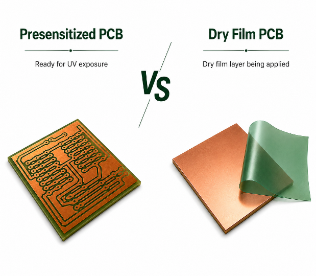
          How Do You Choose a Telecom Board Manufacturer?

          Choosing a telecom board manufacturer requires more than checking price. A good supplier should understand materials, impedance, fabrication, assembly, testing, and project communication.

          Selection FactorWhat to CheckWhy It Matters
          Telecom PCB experienceRF boards, high-frequency boards, network boardsHelps the supplier find risks faster
          Fabrication capabilityMultilayer PCB, impedance control, via platingSupports board performance and production quality
          Material knowledgeFR4, High-Tg FR4, Rogers, PTFE, metal coreHelps match material with application
          PCBA capabilitySMT, BGA, QFN, connectors, testingSupports complete board delivery
          DFM supportLayout, pad, spacing, stack-up, panelization reviewHelps reduce production risk
          Testing optionsElectrical, impedance, AOI, X-ray, functional testHelps confirm quality before shipment
          Production supportPrototype, small batch, mass productionSupports product growth
          Communication speedClear feedback and practical suggestionsReduces mistakes and delays

          First, check whether the manufacturer has experience with telecom PCBs, RF boards, high-frequency boards, and multilayer boards. Experience helps the supplier find risks faster.

          Next, review fabrication capability. The manufacturer should support controlled impedance, multilayer PCB production, fine line control, via plating, surface finishes, and electrical testing.

          If your project needs assembly, choose a supplier with SMT assembly, BGA/QFN experience, AOI, X-ray inspection, component sourcing, and testing support.

          DFM review is also important. It helps find layout and production risks before manufacturing. This step can save time, especially for dense telecom boards or high-frequency boards.

          Finally, consider communication speed. Your supplier should respond clearly, explain risks, and give practical suggestions. This helps reduce mistakes during production.

          Why Choose EBest Circuit as Your Telecom Board Manufacturer?

          EBest Circuit, also known as Best Technology, supports telecom board customers with PCB fabrication, component sourcing, PCBA assembly, testing, and engineering support.

          EBest CapabilityHow It Helps Telecom Board Projects
          One-stop PCB and PCBA serviceCustomers can manage PCB, components, assembly, and testing with one partner.
          DFM and layout review supportEBest helps review spacing, pads, stack-up, impedance, panelization, and assembly risks.
          High-frequency PCB experienceEBest supports FR4, High-Tg FR4, Rogers, ceramic, metal core, and special PCB structures.
          Component sourcing supportEBest helps check part availability, lead time, package match, and supply risks.
          SMT assemblyEBest supports fine-pitch parts, BGA, QFN, connectors, and module-level assembly.
          Inspection and testingAOI, X-ray, electrical testing, and functional testing can support quality control.
          Prototype and batch supportCustomers can move from sample runs to production with a stable process.
          Quality control and traceabilityProduction records and inspection steps support long-term manufacturing needs.

          EBest supports bare PCB fabrication and assembled PCBA production. Therefore, customers can manage PCB, components, assembly, and testing through one manufacturing partner.

          EBest can also review manufacturability-related layout details. These include spacing, pad design, solder mask clearance, stack-up feasibility, impedance needs, panelization, and assembly risk. This support is useful for telecom boards with RF traces, dense parts, or mixed signal and power sections.

          In addition, EBest has experience with FR4, High-Tg FR4, Rogers materials, ceramic PCBs, metal core PCBs, and other special PCB structures. This helps customers choose a better material path for telecom applications.

          For assembly projects, EBest supports SMT assembly for telecom PCBs, including fine-pitch parts, BGA, QFN, connectors, and module-level assemblies. Also, AOI, X-ray inspection, electrical testing, and functional testing can support quality control.

          If you need telecom PCB fabrication, telecom PCB assembly, or one-stop telecom board manufacturing support, contact EBest Circuit at sales@bestpcbs.com for a project review or quotation.

          FAQs About Telecom Board

          1. Is a telecom board the same as a telecom PCB?
          Yes. In PCB manufacturing, a telecom board usually means a telecom PCB or telecom PCBA for communication equipment.

          2. What is the difference between telecom board and telecommunications board?
          The meaning is usually similar. Telecom board sounds shorter, while telecommunications board sounds more formal.

          3. Can FR4 work for telecom circuit boards?
          Yes. FR4 works for many telecom control boards, network boards, and digital communication boards. For RF or low-loss designs, high-frequency materials may work better.

          4. When should a telecom board use Rogers materials?
          Rogers materials suit RF, microwave, antenna, and high-frequency telecom boards that need lower signal loss and stable dielectric performance.

          5. Does every telecom board need impedance control?
          No. However, boards with RF traces, differential pairs, Ethernet lines, or high-speed signals often need controlled impedance.

          6. What does EBest check during telecom PCB layout review?
          EBest checks manufacturability items such as spacing, stack-up, impedance needs, pad design, solder mask clearance, panelization, via structure, and assembly risk.

          7. Can EBest provide telecom PCB assembly?
          Yes. EBest supports telecom PCB assembly, including SMT assembly, component sourcing, BGA/QFN assembly, AOI, X-ray inspection, and testing support.

          8. What files should I provide for a telecom board quotation?
          You can provide Gerber files, BOM, pick-and-place file, assembly drawing, stack-up requirements, impedance requirements, material preference, quantity, and testing needs.

          9. How do I choose a telecom board manufacturer?
          Choose a supplier with telecom PCB experience, material knowledge, impedance control, PCBA assembly, testing support, DFM review, and clear communication.

          You may also like