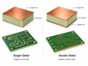
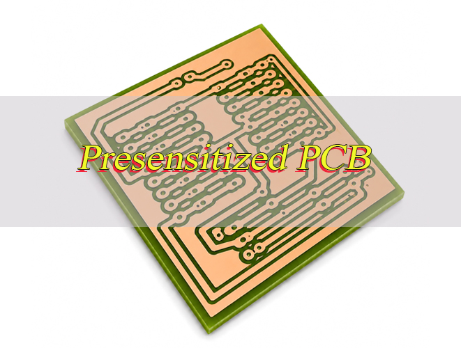
A presensitized PCB is a pre-coated copper clad board used to transfer circuit patterns with UV light, developer and chemical etching. It is mainly used for prototype circuits, electronics learning, repair testing and simple low-volume PCB experiments.
The process looks simple, but the result depends on artwork density, board storage, exposure control, developer strength and etching time. For basic circuits, this material offers a fast way to make a board without coating photoresist by hand. For repeatable production, it also helps users understand why professional PCB imaging and quality control matter.
What Is a Presensitized PCB?
A presensitized PCB is a copper clad board with a light-sensitive resist layer already applied to the copper surface. During exposure, UV light reacts with selected areas of the coating through printed artwork.
Most boards are positive presensitized PCB products. In this format, the exposed resist becomes removable in developer, while the unexposed resist stays on the copper and protects the circuit image during etching.
This board type is useful for fast prototypes and simple circuit tests. However, it does not replace full PCB manufacturing when plated through holes, solder mask, fine-pitch assembly, controlled impedance or certified production quality is required.
What Is a Presensitized PCB Board Made Of?
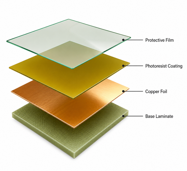
A presensitized PCB board is made of base laminate, copper foil, photosensitive resist and a protective film. Each layer affects mechanical strength, image quality and final etching accuracy.
| Layer | Material | Purpose |
|---|---|---|
| Base | FR4, CEM, phenolic | Insulation and support |
| Copper | Copper foil | Traces and pads |
| Resist | Positive photoresist | Image transfer |
| Film | Light-blocking film | Surface protection |
A presensitized copper clad board should stay sealed before use. Heat, humidity and light can weaken the coating, so storage quality directly affects exposure contrast and trace definition.
How to Cut Presensitized PCB Board?
A presensitized PCB board should be cut before exposure, with the protective film still attached. This keeps the photoresist surface safe from scratches, dust and accidental light exposure.
Step 1: Keep the protective film on.
Do not peel the film before cutting. The coating is light-sensitive and easy to damage, so the film should stay in place until the board is ready for artwork alignment.
Step 2: Mark the board size.
Mark the cutting line according to the PCB outline or prototype size. Leave a small edge margin around traces, pads and mounting holes to avoid damaging the circuit area.
Step 3: Use a suitable cutting tool.
For thin boards, a scoring knife or PCB shear is usually enough. For thicker FR4 boards, use a small saw, rotary cutter or PCB cutting machine. Keep the board flat during cutting to prevent cracks or laminate stress.
Step 4: Remove burrs carefully.
After cutting, smooth the edge with fine sandpaper or a small file. Do this gently and keep dust away from the coated surface.
Step 5: Clean before exposure.
Remove loose dust with clean air or a lint-free method. Do not rub the resist surface hard. Once the board is clean, align the artwork and continue with exposure.
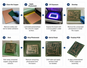
How to Make a Presensitized PCB?
To make a presensitized PCB, you need to prepare the artwork, expose the coated board, develop the image, etch the copper, clean the board and drill the holes. The process is simple, but each step affects the final circuit quality.
Step 1: Prepare clear artwork.
Print the PCB pattern on transparent film. The black areas should be dark and sharp enough to block UV light. If the artwork is weak, traces may become thin or incomplete.
Step 2: Cut and clean the board.
Cut the board to the required size before exposure. Keep the protective film on during cutting, then remove dust and particles from the surface area.
Step 3: Align the artwork.
Peel off the protective film only when the board is ready for exposure. Place the artwork tightly against the coated copper surface. Good contact helps create clean trace edges.
Step 4: Expose the board.
Use a UV exposure unit with stable light and timing. Start with a small test strip if the board, lamp or artwork is new. This helps avoid underexposure or overexposure.
Step 5: Develop the image.
Place the exposed board into the correct developer. Stop when the unwanted resist is removed and the copper pattern is clear. Do not keep developing after the image is already visible.
Step 6: Check the pattern before etching.
Inspect the traces, pads and clear copper areas. If the image is weak, blurry or broken, fix the exposure or development problem before etching.
Step 7: Etch the copper.
Put the board into the etchant and move the solution gently. When unwanted copper is removed, rinse the board immediately to stop chemical action.
Step 8: Drill and inspect.
Drill component holes after etching. Then check for shorts, open traces, thin pads and copper residue. For important prototypes, test continuity with a multimeter before soldering.

What Exposure Time Is Needed for Presensitized PCB?
Presensitized PCB exposure time depends on UV intensity, wavelength, lamp distance, artwork opacity, resist sensitivity and board age. A fixed time from another setup should only be used as a starting point.
| UV Source | Range | Control Point |
|---|---|---|
| UV exposure box | 2–5 minutes | Repeatable timing |
| UV LED lamp | 3–8 minutes | Distance and wavelength |
| UV tube | 5–10 minutes | Uniform coverage |
| Sunlight | Unstable | Poor repeatability |
For this reason, a small test strip is the safest method. Underexposure leaves weak image contrast and copper residue. Overexposure can narrow traces, remove small pads and make fine details difficult to keep.
What UV Exposure Unit Is Best for Presensitized PCB?
The best UV exposure unit for presensitized PCB work is a UV LED exposure box with even light, a stable timer, firm artwork contact and repeatable board placement. It gives more reliable results than sunlight or a handheld UV lamp.
Even light distribution is the first requirement. If the light is uneven, one part of the board may be overexposed while another part remains underexposed. This can cause thin traces, missing pads or poor development.
A timer is also important. Presensitized PCB exposure time changes with lamp power, distance, artwork density and board age. A stable timer makes each test repeatable and reduces failed boards.
Good artwork contact is another key point. The film should sit flat against the photoresist surface. If there is an air gap, trace edges may become blurry. For most prototype work, a compact UV LED box with a flat glass plate, safety cover and fixed distance is a good choice.
What Developer Is Used for Presensitized PCB?
The developer is usually a mild alkaline solution matched to the photoresist type, and many positive boards use sodium hydroxide-based chemistry. The safest ratio is always the supplier’s recommended concentration.
Presensitized PCB developer sodium hydroxide must be handled carefully. If the solution is too strong, it can remove good resist and destroy the circuit image. If it is too weak, exposed resist may remain on the copper and block etching.
Use gloves, eye protection and a clean plastic container. Development should stop when the copper areas to be etched are fully visible. After that, rinse the board gently and inspect the pattern before moving to etching.
How Does the Presensitized PCB Etching Process Work?
The presensitized PCB etching process removes exposed copper while the remaining resist protects the required traces, pads and copper areas. In this process, the resist works as a temporary chemical barrier.
Step 1: Confirm the developed image.
Before etching, check that the unwanted resist has been removed and the copper areas to be etched are fully exposed. If the image is incomplete, do not start etching yet.
Step 2: Prepare the etchant.
Ferric chloride and ammonium persulfate are common choices for small PCB work. The etchant should be active, clean and suitable for the copper thickness. Weak or exhausted solution can leave copper residue.
Step 3: Place the board into the solution.
Put the board into the etchant carefully and make sure the copper surface is fully covered. Do not scrape the resist surface, because damaged resist can cause broken traces.
Step 4: Move the solution gently.
Gentle movement helps fresh chemical reach the copper surface. Etching speed changes with copper thickness, temperature, chemical strength and agitation. Avoid aggressive movement that may damage fine patterns.
Step 5: Stop when unwanted copper is gone.
Do not leave the board in the etchant longer than needed. Over-etching can narrow traces, weaken pads and reduce dimensional accuracy.
Step 6: Rinse and inspect immediately.
Rinse the board with clean water as soon as etching is complete. Then check for shorts, open traces, thin pads, copper residue and damaged edges before drilling or soldering.
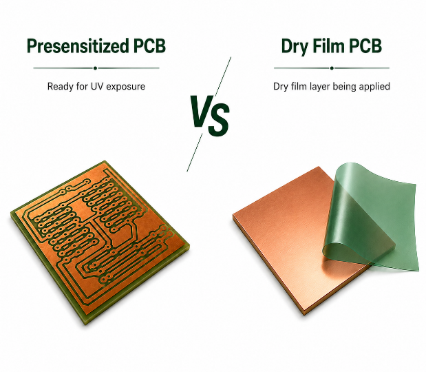
What Is the Difference Between Presensitized PCB and Dry Film PCB?
Presensitized PCB vs dry film is mainly a choice between easier setup and stronger process control. A presensitized board is ready to expose, while dry film needs lamination before exposure.
| Point | Presensitized PCB | Dry Film PCB |
|---|---|---|
| Setup | Faster and simpler | Requires lamination |
| Equipment | UV unit and developer | Laminator, UV unit and developer |
| Skill Level | Easier for beginners | Better for experienced users |
| Coating | Factory pre-coated | Applied by the user |
| Main Risk | Old coating or wrong exposure | Bubbles, wrinkles or poor adhesion |
| Fine Traces | Good for simple prototypes | Better when lamination is well controlled |
| Storage | Board coating ages over time | Film and copper board stored separately |
| Cost Control | Convenient for small tests | Flexible for repeated prototype work |
| Best Use | Learning, repair and simple boards | Controlled prototype production |
For beginners, a positive acting presensitized PCB board is usually easier to handle. For users with proper cleaning, lamination pressure and temperature control, dry film can offer more flexibility for repeated prototype work.
What Common Problems Happen When Using Presensitized PCBs?
Common problems include faint images, thin traces, copper residue, broken tracks, bridged pads, over-etching and double-sided misalignment. Most issues come from artwork quality, exposure time, developer strength, etching control or poor storage.
- Faint image: The board may be underexposed, the UV source may be weak, or the material may be old. Use a test strip, check lamp distance and make sure the artwork is pressed flat.
- Thin traces: This usually comes from overexposure, weak black artwork or excessive development. Reduce exposure time, improve artwork density and stop development once the image is clear.
- Copper residue: The exposed resist may not be fully removed, or the etchant may be weak. Check the developed image before etching and replace exhausted etchant when copper removal becomes slow.
- Broken tracks: Scratches, dust and over-etching can cut narrow traces. Keep the coating clean, avoid hard rubbing and rinse the board as soon as etching is complete.
- Bridged pads: Blurry artwork, poor contact or incomplete etching can leave copper between pads. Use sharper artwork, improve film contact and continue etching only until unwanted copper is gone.
- Double-sided mismatch: Top and bottom patterns can shift if the films are not aligned correctly. Use registration holes and check pad-to-hole matching before exposure.
- Uneven results: Uneven UV light, unstable developer strength or poor etchant movement can cause inconsistent patterns across the board. A controlled UV box and gentle chemical movement improve repeatability.
How Long Is the Shelf Life of Presensitized PCB?
Presensitized PCB shelf life is limited because the photosensitive coating slowly changes with time, light, heat and humidity. The exact storage period depends on the manufacturer and package quality.
Old boards may need longer exposure, develop unevenly or fail to hold fine traces. Once a pack is opened, unused material should be resealed, kept flat and stored in a dark, cool and dry place.
Before using old stock for an important circuit, expose a small test piece first. If the image looks weak, patchy or unstable during development, replacing the material is more reliable than changing every process setting.
How Much Does Presensitized PCB Price Usually Depend On?
Presensitized PCB price usually depends on board size, base laminate, copper thickness, single or double sided structure, package content, shelf condition and supplier reliability. The lowest price may not be the best value if the coating is old or uneven.
| Factor | Impact | Buying Note |
|---|---|---|
| Size | Larger area costs more | Match real design size |
| Side | Double sided costs more | Check alignment needs |
| Copper | Thicker copper costs more | Etching takes longer |
| Base | FR4 costs more | Better strength |
| Pack | Kit pricing varies | Check shelf life |
| Supplier | Storage affects quality | Avoid unknown old stock |
A presensitized PCB pack can be useful for learning or lab use because it may include boards and developer. For production-ready projects, custom PCB fabrication is usually more stable because it includes controlled imaging, solder mask, drilling, plating, inspection and electrical testing.
FAQs About Presensitized PCB
Q1: Can this board support fine traces?
A1: Yes, but only within the limits of artwork quality, exposure control and etching accuracy. Simple fine traces can work well when the film is sharp and pressed tightly against the board. For very narrow spacing or repeatable production, factory PCB fabrication is more reliable.
Q2: What copper thickness is commonly used?
A2: A common copper thickness is 1 oz, about 35 μm. Thicker copper can carry more current, but it takes longer to etch and may reduce edge accuracy. For simple prototypes, standard copper is easier to process.
Q3: Can it be used for SMD components?
A3: Yes, simple SMD layouts can work. The main risks are solder bridges, pad undercut and missing solder mask. For fine-pitch ICs, dense pads or assembly production, a factory-made PCB with solder mask is a better option.
Q4: Does it need solder mask?
A4: A basic test board can work without solder mask, but exposed copper oxidizes more easily. Solder mask improves insulation, soldering control and surface protection. It is strongly recommended for commercial products or dense SMD designs.
Q5: Can it make plated through holes?
A5: No, normal exposure and etching cannot make plated through holes. Plated holes need drilling, hole wall activation, copper deposition and electroplating. If the design needs vias or plated component holes, use professional PCB manufacturing.
Q6: What artwork film is best?
A6: Use transparent film with high resolution and strong black density. Weak black areas allow UV light to leak through and may make traces thinner. The film should be clean, flat and tightly attached to the coated surface.
Q7: Can the developer be reused?
A7: It can be reused for simple boards, but the result becomes less stable over time. Photoresist residue weakens the solution. For fine traces or important boards, fresh developer gives better control.
Q8: Is sodium hydroxide developer dangerous?
A8: Yes, sodium hydroxide is corrosive. Use gloves, eye protection and proper ventilation. Mix the solution according to the supplier’s instructions and avoid skin contact. A solution that is too strong can also damage the circuit image.
Q9: Can drilling be done before exposure?
A9: Yes, especially for double-sided alignment, but dust must be removed carefully. Any particle on the coating can block UV light. For simple single-sided boards, drilling after etching is usually cleaner.
Q10: Is it suitable for RF circuits?
A10: Only simple RF experiments are suitable. RF and antenna designs often need controlled impedance, stable dielectric material and precise trace geometry. For commercial RF products, professional PCB fabrication is recommended.
Q11: Can it be used for mass production?
A11: It is not ideal for mass production. Manual exposure, development and etching create variation. Factory PCB production provides controlled imaging, drilling, plating, solder mask, electrical testing and final inspection.
Q12: What files are needed for a factory PCB quote?
A12: Gerber files, drill files, board thickness, copper thickness, solder mask color, surface finish, quantity and assembly requirements are the main details. If the prototype has been tested, also share current, voltage and application environment.
Conclusion
Presensitized PCB is a practical material for learning, repair testing and simple prototype verification. Its result depends on artwork quality, UV exposure, developer control, etching stability and careful handling. It is useful for early experiments, but it is not the best choice for plated holes, solder mask, fine-pitch assembly or repeatable production.
For stable PCB production, choose a supplier with strong material control, fabrication capability, inspection process and assembly support. EBest Circuit is a China source factory supporting custom PCB manufacturing, PCB assembly, OEM/ODM projects and global supply. Send your Gerber files, BOM and project requirements to sales@bestpcbs.com for a quotation.