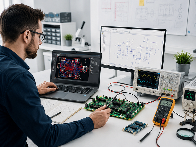
Electronic product design & test is the complete process of turning an electronic idea into a stable, manufacturable, and testable product. It covers circuit design, PCB layout, component selection, prototype validation, functional testing, reliability checks, and preparation for mass production.
At Best Technology, our engineering work is closely connected with PCB fabrication, component sourcing, PCB assembly, prototype builds, and mass production. This gives customers a practical advantage: design decisions can be checked from the manufacturing side before they become expensive production problems. For projects that need OEM manufacturing, ODM development, sample validation, or custom engineering support, electronic product design and testing should begin before the first PCB is ordered.
What Is Electronic Product Design & Test?
Electronic product design & test means designing an electronic device and verifying that it works safely, reliably, and consistently before full production.
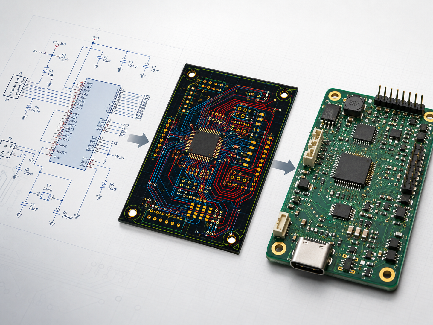
The design part usually includes product requirements, circuit architecture, schematic design, PCB layout, firmware coordination, enclosure fit, thermal planning, power design, and component selection. The test part checks whether those decisions perform correctly in real hardware.
In a PCB-based product, design and testing are strongly connected. A board may pass a basic power-on test but still fail under vibration, heat, EMI exposure, long operating time, or load changes. That is why professional electronic product testing does not stop at “does it turn on?” It checks function, stability, manufacturability, and production repeatability.
| Area | What It Covers | Why It Matters |
|---|---|---|
| Circuit design | Schematic, power rails, signal paths, protection circuits | Defines the product’s electrical behavior |
| PCB layout | Stack-up, routing, grounding, impedance, spacing | Affects EMI, heat, reliability, and assembly |
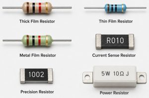
| Component selection | ICs, passives, connectors, sensors, power devices | Controls cost, availability, and lifecycle risk |
| Prototype testing | Bring-up, debugging, measurement, modification | Finds design issues before tooling or batch orders |
| Functional testing | Input/output behavior, firmware response, load operation | Confirms the product performs its intended function |
| Reliability testing | Thermal, aging, vibration, humidity, cycling | Reduces field failure risk |
| Production testing | ICT, FCT, AOI, X-ray, final inspection | Ensures batch consistency |
In short, electronic product design & test is the bridge between an idea and a product that can be manufactured repeatedly.
Why Is Electronic Product Design & Test Important?
Electronic product design & test is important because most product failures are cheaper to solve during design than after mass production.
A common mistake is treating testing as the final step. In reality, testing should influence the design from the beginning. Test points, programming access, fixture access, connector orientation, thermal margins, and inspection visibility all need to be planned early.
For example, if a PCB has no test pads for key voltage rails, factory functional testing becomes slower and less stable. If an RF trace is routed without proper impedance control, the prototype may work in a short bench test but fail in certification or long-range communication. If a high-current path is too narrow, the board may pass a short load test but overheat after extended use.
How Does Electronic Product Design & Test Work from Concept to Mass Production?
Electronic product design & test usually follows a staged process: requirement definition, design, prototype, validation, pilot run, and mass production.
The process starts with a clear product requirement. This includes input voltage, output power, operating temperature, expected lifetime, communication interface, mechanical size, certification market, and production volume. Without these details, engineers may design a board that works electrically but does not fit the enclosure, pass compliance, or meet cost targets.
For many hardware teams, EVT, DVT, and PVT are useful checkpoints. EVT checks whether the engineering concept works. DVT checks whether the design meets product requirements under more realistic conditions. PVT checks whether the product can be built consistently in a production environment.
What Are the Main Types of Electronic Product Design Services?
Electronic product design services can be divided into concept design, circuit design, PCB design, firmware coordination, mechanical integration, and production engineering.
Different customers need different service depth. Some customers already have a complete schematic and only need PCB layout optimization. Others have an idea, enclosure size, and performance target but need full ODM development.
| Service Type | Suitable For | Key Deliverables |
|---|---|---|
| Concept-to-prototype design | Startups, new product teams | Architecture, schematic, PCB, sample |
| Schematic design | Customers with clear function requirements | Circuit diagram, BOM, design notes |
| PCB layout design | Hardware teams with existing schematic | PCB layout, Gerber, stack-up |
| DFM/DFT review | Buyers preparing production | Manufacturing and testability feedback |
| Prototype development | Teams before certification or tooling | Sample PCBA, debug support |
| Firmware coordination | Embedded electronics projects | Firmware interface support |
| Component sourcing | OEM/ODM production buyers | AVL, BOM review, lifecycle check |
| PCBA manufacturing | Product brands and equipment companies | SMT, DIP, testing, final assembly |
The best service model depends on how mature the project is. A mature design may only need design-for-manufacturing review and assembly testing. An early-stage idea needs deeper engineering support before PCB production begins.
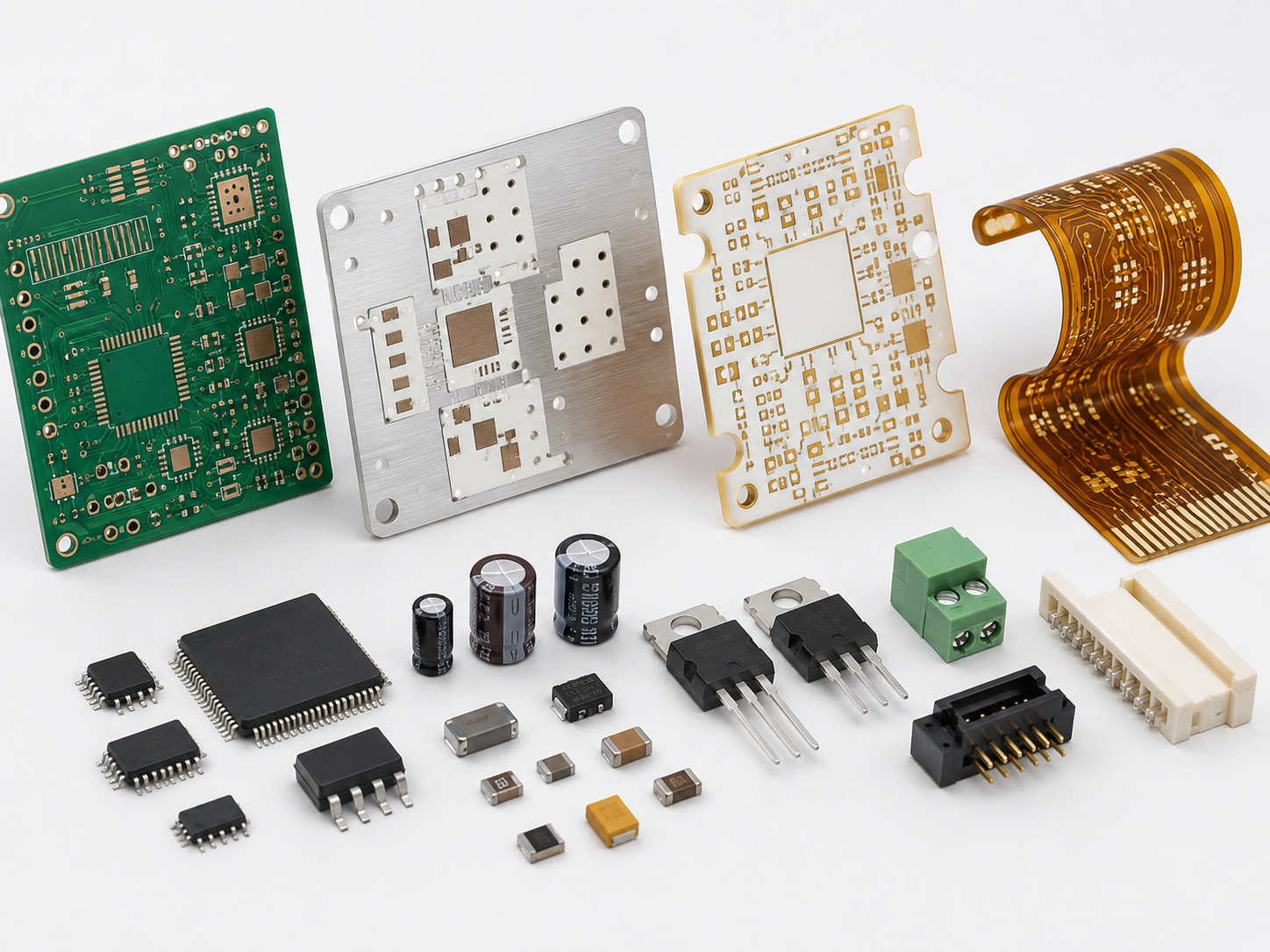
Which Materials and Components Matter Most in Electronic Product Design?
For PCB-based products, material selection is not only about choosing FR4. The correct material depends on frequency, heat, voltage, mechanical structure, size, and environment. A low-power sensor may work well on standard FR4. A high-power LED product may need aluminum PCB or copper base PCB. A high-frequency communication product may need RF material with stable dielectric properties.
| Design Item | Common Options | Selection Concern |
|---|---|---|
| PCB material | FR4, high Tg FR4, aluminum, copper base, ceramic, flexible PCB | Heat, frequency, cost, reliability |
| Copper thickness | 1 oz, 2 oz, heavy copper | Current capacity and thermal rise |
| Surface finish | HASL, lead-free HASL, OSP, ENIG, immersion silver | Solderability, flatness, storage life |
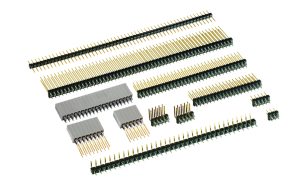
| Connectors | Wire-to-board, board-to-board, terminal blocks | Current, vibration, mating cycle |
| Capacitors | MLCC, electrolytic, tantalum, film | Ripple current, polarity, voltage margin |
| Power devices | MOSFET, diode, regulator, driver IC | Heat, efficiency, switching speed |
| Sensors | Temperature, pressure, motion, optical | Accuracy, calibration, interface |
| Protection parts | TVS diode, fuse, NTC, MOV | Surge, ESD, overload protection |
Component availability is also a design issue. A product may fail commercially if it depends on a part with long lead time, unstable supply, or a short lifecycle. For production projects, the BOM should be reviewed for alternatives, package availability, brand approval, and procurement risk before pilot production.
What Tests Are Used to Validate an Electronic Product?
Electronic product testing includes electrical tests, functional tests, reliability tests, safety checks, and production inspections.
The exact test plan depends on the product type. A medical device, automotive controller, LED driver, smart home module, and industrial sensor will not need the same test depth. However, most PCB-based products share several basic test layers, including:
| Test Type | What It Checks | Typical Method |
|---|---|---|
| Visual inspection | Assembly defects, solder quality, missing parts | Manual inspection, AOI |
| Electrical test | Shorts, opens, resistance, voltage rails | Multimeter, flying probe, ICT |
| Functional test | Whether the device performs its intended task | Custom test fixture, firmware test |
| Power test | Load behavior, efficiency, ripple, startup | Power supply, oscilloscope, load meter |
| Thermal test | Heat rise, hot spots, thermal stability | Thermal camera, chamber test |
| Signal test | Clock, waveform, impedance, communication | Oscilloscope, logic analyzer, VNA |
| Aging test | Long-time operation stability | Burn-in rack, cycling test |
| Environmental test | Heat, humidity, vibration, thermal shock | Environmental chamber, vibration table |
| Safety test | Insulation, creepage, clearance, protection | Hi-pot, leakage, safety review |
| Production test | Batch repeatability | ICT, FCT, AOI, X-ray, final QC |
For assembled PCBs, AOI is useful for visible solder and placement defects. X-ray is important for hidden solder joints such as BGA, QFN thermal pads, and some through-hole conditions that cannot be fully inspected from the surface. Functional circuit testing checks whether the real product works under controlled factory conditions.
What Standards Should Be Considered During Electronic Product Design & Test?
For PCB and PCBA projects, IPC standards are commonly used for design, assembly workmanship, soldering process control, and acceptability. IPC-2221 is widely used as a foundation design standard for printed boards. IPC J-STD-001 focuses on soldered electrical and electronic assemblies. IPC-A-610 is commonly used for acceptability of electronic assemblies.
For products entering specific markets, safety and compliance requirements may also apply. IEC 62368-1 is widely relevant to audio/video, information, and communication technology equipment. Products with radio frequency functions may need FCC-related authorization for the U.S. market. Products entering the EU may need RoHS compliance for hazardous substance restrictions.
| Area | Common Reference | Practical Meaning |
|---|---|---|
| PCB design | IPC-2221 series | Printed board design requirements |
| Soldered assemblies | IPC J-STD-001 | Soldering materials, methods, and process criteria |
| Assembly acceptance | IPC-A-610 | Visual acceptability for electronic assemblies |
| Product safety | IEC 62368-1, IEC 61010, IEC 60601 depending on product | Safety requirements by product category |
| Environmental compliance | RoHS, REACH where applicable | Restricted substances and material declarations |
| Wireless/RF product | FCC, CE RED depending on target market | RF emission and equipment authorization |
| Automotive electronics | IATF 16949 system, customer-specific requirements | Process control and traceability |
| Medical electronics | ISO 13485 system, applicable medical device standards | Quality management and risk control |
How to Choose the Right Design and Test Plan for Your Product?
The right design and test plan should match product risk, operating environment, market requirements, and production volume.
A simple consumer LED module may need schematic review, PCB layout, prototype testing, thermal check, and functional testing. A medical or automotive-related control board may need deeper documentation, traceability, reliability testing, risk analysis, and stricter inspection.
Use these questions before choosing the test plan:
- What is the product’s input voltage and maximum current?
- Will it operate continuously or intermittently?
- What is the operating temperature range?
- Does it contain RF, high-speed signals, motors, relays, batteries, or high-voltage sections?
- Will it be used in consumer, industrial, automotive, medical, or outdoor environments?
- What certifications or customer standards are required?
- What is the expected production quantity?
- What failure would be most costly: safety issue, downtime, warranty return, or certification delay?

Which Industries Need Electronic Product Design & Test?
Electronic product design & test is needed wherever hardware must perform reliably after shipment.
The demand is especially strong in industries where PCB failure can cause downtime, safety concerns, service cost, or brand damage. These industries need more than basic PCB assembly. They need design review, process control, and test coverage matched to real operating conditions.
| Industry | Typical Products | Main Design and Test Concerns |
|---|---|---|
| Industrial control | PLC modules, sensors, motor controllers | Noise immunity, connectors, long service life |
| Medical electronics | Monitoring devices, diagnostic modules | Reliability, traceability, safety-related design |
| Automotive electronics | Lighting, control modules, charging systems | Vibration, temperature, process control |
| LED lighting | Drivers, aluminum PCBs, power modules | Heat dissipation, current stability |
| Smart home | Wi-Fi modules, sensors, control boards | RF performance, power consumption, safety |
| Consumer electronics | Chargers, handheld devices, audio products | Cost, size, user safety, durability |
| Communication equipment | RF boards, network devices, antennas | Impedance, EMI, signal integrity |
| Energy products | Battery systems, inverters, power boards | High current, protection, thermal design |
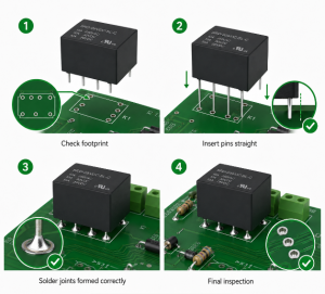
What Should Engineers Check Before PCB Manufacturing and Assembly?
Before PCB manufacturing and assembly, engineers should check manufacturability, testability, component risk, and production documentation.
If you required PCB assembly, then a clean Gerber package alone is not enough. The manufacturer also needs BOM, pick-and-place file, assembly drawing, test requirements, surface finish, material specification, copper thickness, impedance needs, and any special process notes.
| Checklist Item | What to Confirm | Why It Matters |
|---|---|---|
| Gerber and drill files | Correct revision, complete layers, drill data | Prevents wrong board fabrication |
| Stack-up | Thickness, material, copper weight, impedance | Controls electrical and mechanical performance |
| BOM | Part number, brand, package, alternatives | Reduces sourcing and assembly risk |
| Footprints | Pad size, polarity, pin orientation | Avoids soldering and placement errors |
| Test points | Power rails, signals, programming pads | Improves fixture testing |
| Thermal design | Copper area, vias, metal core need | Controls hot spots |
| Creepage and clearance | High-voltage spacing | Supports safety requirements |
| DFM review | Minimum trace, spacing, annular ring, solder mask | Improves manufacturability |
| DFT review | Fixture access, test sequence, pass/fail limits | Improves production consistency |
| Inspection plan | AOI, X-ray, ICT, FCT | Matches product risk |
| Packaging | ESD protection, moisture control, labeling | Prevents transport and storage damage |
The best time to find these problems is before fabrication. Once PCBs are built and components are mounted, even a small design correction can require new boards, new stencils, and a new validation cycle.
What Affects the Cost of Electronic Product Design & Test?
The cost of electronic product design & test depends on design complexity, validation depth, component risk, PCB structure, test fixture needs, and production volume.
A simple two-layer control board is very different from a high-speed, high-current, RF, or medical-related product. The more constraints a product has, the more engineering time and test coverage it usually needs.
| Cost Factor | Why It Changes Cost |
|---|---|
| Circuit complexity | More power rails, ICs, interfaces, and protection circuits need more design time |
| PCB layer count | Multilayer boards require more layout planning and manufacturing control |
| Signal speed | High-speed and RF designs need impedance control and measurement |
| Thermal demand | High-power products may need aluminum, copper base, ceramic, or extra copper |
| Component availability | Hard-to-source parts increase BOM review and procurement work |
| Firmware interaction | Embedded testing may require programming and debugging support |
| Test fixture | Custom fixtures improve speed but add upfront cost |
| Reliability test depth | Aging, thermal cycling, vibration, and humidity testing increase validation cost |
| Compliance target | Safety, EMC, RF, or medical requirements add review and lab testing |
| Production quantity | Higher volume often justifies better fixtures and stricter process control |
Cost control should start with design decisions. Choosing a stable component package, avoiding unnecessary layer count, planning test pads, and using a manufacturable PCB structure can reduce total project cost without weakening product quality.
How to Choose a Reliable Electronic Product Design & Test Supplier?
A reliable supplier should understand both engineering design and manufacturing reality.
Many design problems happen because the design team and factory team work separately. The design may look elegant, but the PCB may be difficult to fabricate, hard to assemble, or slow to test. A better supplier can review the project from the full product path: schematic, PCB layout, BOM, fabrication, PCBA, testing, and shipment.
When selecting a supplier, check these points:
- Can they support PCB design, prototyping, component sourcing, PCB assembly, and mass production?
- Do they review DFM and DFT before production?
- Can they explain which tests are needed and which are unnecessary?
- Do they support AOI, X-ray, functional testing, and engineering feedback?
- Can they handle custom PCB materials such as FR4, aluminum, copper base, ceramic, flexible PCB, rigid-flex PCB, or high-frequency PCB?
- Do they understand OEM and ODM project workflows?
- Can they support small-batch samples and later volume production?
- Do they provide clear communication on technical files, BOM issues, and production risks?
For global buyers sourcing from a China-based source factory, the advantage is often stronger cost control, flexible customization, and direct manufacturing communication. The important point is transparency. A supplier should not claim fake local factories or local warehouses. Instead, it should clearly explain how engineering support, production, inspection, shipping, and documentation are handled.
Best Technology supports customers who need PCB design, PCB prototype, component sourcing, PCB assembly, and mass production from one engineering and manufacturing workflow. This is especially useful when customers need fast samples, custom PCB structures, or production feedback before placing larger orders.
Common Failure Analysis in Electronic Product Design & Test
In real projects, failures are often caused by several small issues rather than one obvious mistake. A product may fail because of marginal component selection, weak thermal design, solder joint stress, firmware timing, poor grounding, or insufficient test coverage.
| Failure Symptom | Possible Root Cause | Practical Correction |
|---|---|---|
| Board does not power on | Short circuit, wrong polarity, missing component | Electrical test, BOM check, polarity review |
| Random reset | Power ripple, poor decoupling, firmware watchdog issue | Oscilloscope test, capacitor placement review |
| Overheating | Narrow copper path, weak heat spreading, poor airflow | Thermal simulation, copper increase, material change |
| Communication error | Impedance mismatch, EMI, grounding issue | Layout review, shielding, signal measurement |
| High defect rate | Poor footprint, solder mask issue, weak process window | DFM review, stencil tuning, AOI feedback |
| Field failure | Environment not tested, vibration, humidity, aging | Reliability test and material review |
| Certification delay | EMI or safety spacing issue | Pre-compliance review and layout correction |
What Files Should You Prepare Before Requesting a Quote?
Before requesting a quote for electronic product design & test, prepare clear technical files and project requirements.
If the project is still at the idea stage, a block diagram, product function description, target size, expected power input, and use environment are helpful. If the project already has PCB files, send the Gerber, BOM, schematic, pick-and-place file, test requirements, and quantity.
| File or Information | Why It Helps |
|---|---|
| Product function description | Helps engineers understand the design target |
| Schematic | Allows circuit review and debugging |
| Gerber files | Needed for PCB fabrication review |
| BOM | Allows component sourcing and assembly quotation |
| Pick-and-place file | Needed for SMT programming |
| Assembly drawing | Shows polarity, placement notes, and mechanical details |
| Test requirements | Defines pass/fail criteria |
| Sample or reference product | Helps compare function and structure |
| Target market | Helps identify compliance concerns |
| Quantity forecast | Helps choose prototype, pilot, or mass production strategy |
Clear files lead to faster quotation and fewer misunderstandings. They also allow the supplier to provide useful feedback before production starts.
FAQs
Q1: What is the difference between electronic product design and PCB design?
Electronic product design is the broader process. It includes product function, circuit architecture, schematic design, PCB layout, component selection, firmware coordination, testing, enclosure fit, and production planning. PCB design is one important part of that process. It focuses on board structure, routing, stack-up, grounding, spacing, and manufacturability.
Q2: Why should testing be considered during the design stage?
Testing should be planned during design because test access, fixture points, programming pads, and inspection visibility must be built into the PCB. If these items are added after layout, the board may need redesign. Early test planning makes production testing faster, more reliable, and easier to repeat during batch manufacturing.
Q3: What is the first step in electronic product development?
The first step is defining the product requirement. Engineers need to know the function, input voltage, output power, size, operating environment, target market, quantity, and compliance needs. Without these details, the design may work electrically but fail in cost, mechanical fit, certification, or production.
Q4: What tests are required for a new electronic product?
Most products need visual inspection, electrical testing, functional testing, power testing, and basic reliability checks. More complex products may need thermal testing, RF testing, EMI pre-checks, aging tests, vibration testing, humidity testing, or safety testing. The correct test plan depends on product risk and market requirements.
Q5: What is EVT in electronic product testing?
EVT means Engineering Validation Test. It checks whether the early engineering design works as intended. During EVT, engineers usually test power rails, main functions, interfaces, firmware behavior, signal quality, and thermal performance. EVT often produces a list of design changes before the product moves to deeper validation.
Q6: What is the difference between DVT and PVT?
DVT checks whether the completed design meets product requirements under realistic use conditions. PVT checks whether the product can be manufactured consistently through the planned production process. DVT focuses on design maturity. PVT focuses on production readiness, fixture stability, yield, process control, and batch consistency.
Q7: Can a manufacturer help improve my existing electronic product design?
Yes. A manufacturer with engineering capability can review schematic files, PCB layout, BOM, test points, material selection, assembly risk, and production files. This is especially useful when a product has unstable yield, overheating, sourcing problems, EMI concerns, or repeated assembly defects.
Q8: Why does a prototype work but mass production fails?
A prototype may be hand-built, manually tested, or assembled under special attention. Mass production depends on repeatable process windows. Problems often appear when footprints are marginal, test points are missing, components vary, soldering is difficult, or thermal margins are too narrow. Pilot production helps find these risks.
If you need support for electronic product design & test, PCB prototyping, PCB assembly, OEM manufacturing, ODM development, sample validation, or batch production, you can contact our engineering team at sales@bestpcbs.com for technical review and quotation support.