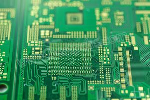
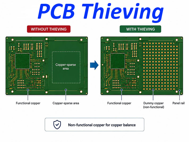
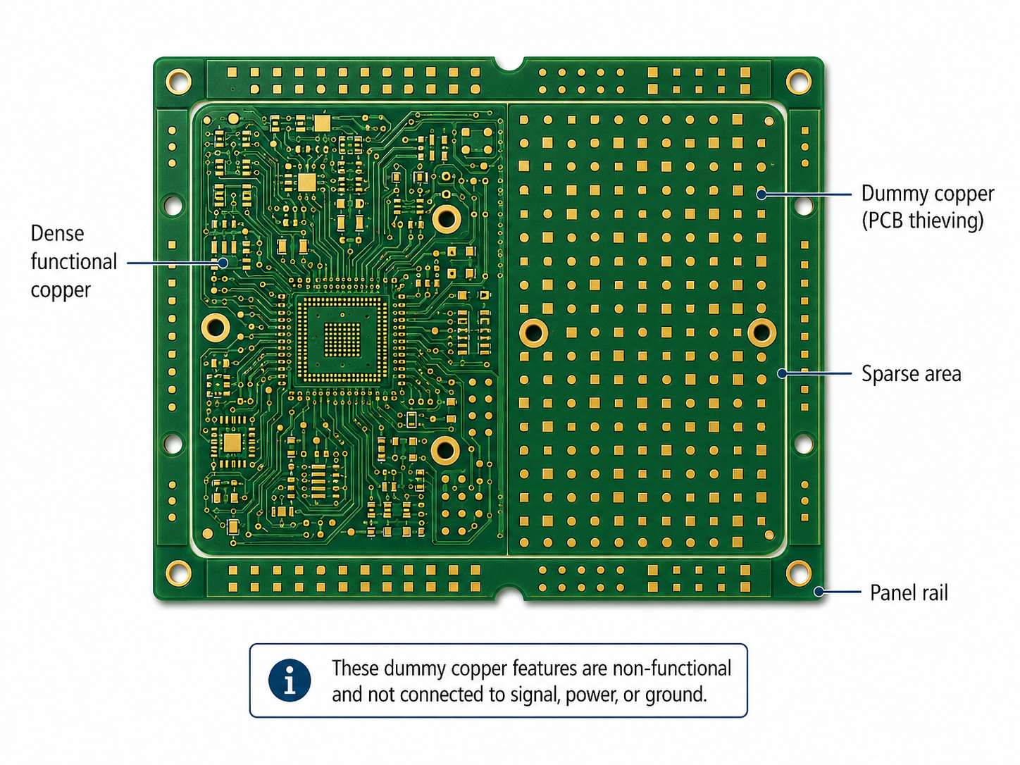
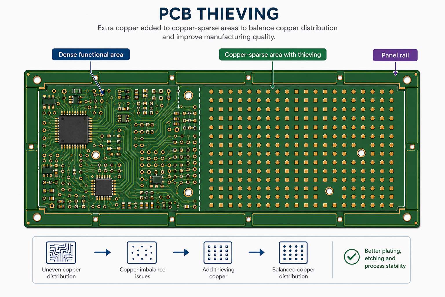
PCB thieving is a non-functional copper pattern added to sparse areas of a PCB or production panel to balance copper distribution, improve plating uniformity, and support stable etching. It usually appears as small copper dots, squares, bars, or grid-like features in open areas. This manufacturing method is especially useful for PCBs with uneven copper density, fine traces, heavy copper, HDI structures, plated through holes, or controlled impedance requirements.
At Best Technology, PCB thieving is reviewed from a manufacturing perspective during CAM and DFM preparation. It is not treated as random copper filling. It must be checked together with copper thickness, spacing, panel layout, impedance requirements, high-voltage clearance, RF areas, solder mask rules, and customer keep-out notes.
Before going deeper, here are the main points to remember:
- PCB thieving is usually non-functional copper.
- It improves manufacturing consistency.
- It helps balance copper density.
- It is different from copper pour.
- It must be controlled near RF, impedance, and high-voltage areas.
- It is often handled during CAM and DFM review.
What Is PCB Thieving?
PCB thieving refers to extra copper features added to unused or copper-sparse areas of a PCB. These copper features normally do not connect to any signal, power, or ground net. They support the fabrication process, not the circuit function.
In simple terms, PCB thieving means placing controlled “dummy copper” where the board has too little copper. This helps reduce the gap between dense copper areas and empty areas.
A PCB may need thieving when it has:
- Dense traces and vias in one area.
- Large blank areas in another area.
- Fine traces that need stable etching.
- Plated holes that need consistent copper deposition.
- Panel borders that need copper balance.
Common names include:
| Term | Simple Meaning |
|---|---|
| PCB thieving | Copper balancing feature |
| Copper thieving | Extra process copper |
| Dummy copper | Non-functional copper |
| Thieving pattern | Dots, squares, or grids |
| Plating thieves | Copper for plating control |
The key point is simple: PCB thieving is not part of the working circuit. It is a manufacturing support feature.
Why Is PCB Thieving Used in PCB Manufacturing?
PCB thieving is used because PCB manufacturing depends heavily on copper distribution. A board with balanced copper is easier to plate, etch, laminate, and finish with stable results.
When copper is unevenly distributed, one area may plate faster, another area may etch differently, and large blank areas may behave differently from dense trace areas. These differences may affect copper thickness, line width, hole wall quality, and production yield.
1. To balance copper density
- Copper density means how much copper exists in a specific area. If one area has a large copper plane and another area has only a few fine traces, the copper distribution is not balanced.
- Thieving copper helps fill sparse regions with controlled non-functional copper. This creates a more even copper layout across the board or production panel.
2. To improve plating uniformity
- During copper electroplating, current distribution matters. Different copper geometries may receive copper at different rates.
- Proper thieving helps make plating more stable. This supports more consistent copper thickness on outer layers and plated through holes.
3. To support etching consistency
- Etching removes unwanted copper to form the final circuit pattern. If copper density varies too much, etching may also vary.
- Thieving copper can reduce local copper density differences. This helps improve trace width control, especially for fine-line PCBs.
4. To reduce manufacturing variation
- PCB fabrication includes many controlled processes. Large copper imbalance can increase variation in plating, etching, lamination, and finishing.
- Thieving patterns help reduce this risk by making the panel more consistent.
5. To improve production yield
- Better copper balance can support better yield. This is especially useful for fine-line PCBs, HDI boards, heavy copper PCBs, large panels, and controlled impedance boards.
- For customers, PCB thieving is not just a small CAM detail. It can help protect final PCB quality.
How Does PCB Thieving Improve Plating Uniformity?
Plating thieving on PCB is mainly related to current distribution during copper electroplating. When a PCB is plated, copper is deposited onto conductive surfaces. The result can be affected by copper pattern, hole density, board size, chemistry, plating current, and panel layout.
If one area has many copper features and another area is almost empty, plating may not distribute evenly. Some areas may receive more copper, while others may receive less. This can affect copper thickness, plated hole quality, and outer layer consistency.
Thieving copper helps by adding controlled conductive features in sparse zones. These features help distribute the plating effect more evenly across the production panel.
| Without Thieving | With Proper Thieving |
|---|---|
| Uneven copper density | Better copper balance |
| Higher plating variation | More stable copper |
| Local over-plating risk | Better current spread |
| Hole plating variation | More consistent plating |
| Less predictable etching | Better process control |
This does not mean every PCB needs heavy thieving. Too much dummy copper may create new risks. Copper placed too close to high-speed traces, RF areas, antennas, or high-voltage gaps may affect performance or safety clearance.
A responsible PCB manufacturer should review thieving together with:
- copper weight
- hole structure
- trace width and spacing
- board size
- panel layout
- controlled impedance areas
- high-voltage clearance
- RF and antenna zones
- customer keep-out requirements
This is why plating thieving is usually handled during CAM and DFM review, not as a simple pattern added anywhere on the board.
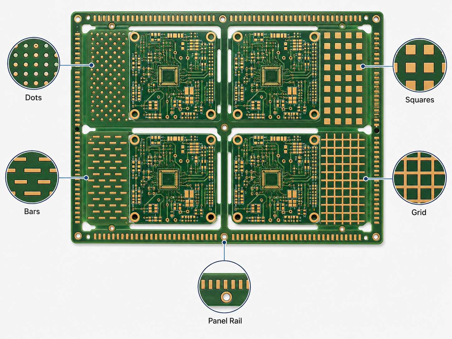
What Does a PCB Thieving Pattern Look Like?
A PCB thieving pattern usually appears as repeated copper features placed in unused spaces or panel borders. These features may look simple, but their size, shape, spacing, and location are chosen for manufacturing control.
Common PCB thieving patterns include:
- Copper dots
- Square copper islands
- Short copper bars
- Grid copper
- Crosshatch copper
- Panel rail thieving
- Custom dummy copper
| Pattern | Appearance | Use |
|---|---|---|
| Dots | Round islands | General balance |
| Squares | Small pads | Density control |
| Bars | Short strips | Local balance |
| Grid | Mesh copper | Large open areas |
| Panel rail | Edge copper | Panel plating |
| Custom | Factory-defined | Special needs |
Small dots and squares are common because they are easy to control. The CAM engineer can adjust the number, spacing, and placement of these features without changing the customer’s functional circuit.
PCB thieving often uses repeated shapes instead of one large copper area for several reasons:
- Copper density can be adjusted more precisely.
- The pattern can stay away from sensitive areas.
- It is easier to inspect during CAM review.
- It reduces the risk of unwanted coupling.
- It gives the manufacturer more process control.
A large copper block may look cleaner, but it may not be the best choice. It can affect spacing, impedance, RF behavior, or solder mask design if placed incorrectly. Repeated thieving patterns give better control.
This is also why customers should not add random dummy copper without checking with the PCB manufacturer. A pattern that looks acceptable in layout software may not match the actual fabrication process.
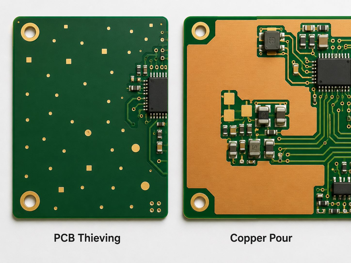
PCB Thieving vs Copper Pour: What Is the Difference?
PCB thieving and copper pour are easy to confuse because both involve copper in open areas. However, they serve different purposes.
Copper pour belongs to the circuit. PCB thieving belongs to the manufacturing process.
Copper pour is usually connected to a net, such as GND, power, or shielding. It may help with return paths, heat spreading, current capacity, EMI control, or voltage reference stability.
PCB thieving is usually isolated copper. It is normally not connected to any electrical net. Its purpose is to improve copper balance and manufacturing consistency.
| Item | PCB Thieving | Copper Pour |
|---|---|---|
| Purpose | Manufacturing balance | Circuit function |
| Net | Usually isolated | Usually connected |
| Added by | CAM/manufacturer | Layout engineer |
| Main value | Plating and etching | Ground, power, heat |
| Common area | Sparse areas, rails | Functional areas |
This difference is important for customers. If copper must support circuit performance, it should be defined in the PCB layout and connected to the correct net. If copper is only needed to improve fabrication balance, it is better reviewed as thieving copper during CAM preparation.
A good PCB manufacturer will not treat all copper the same. Functional copper, dummy copper, copper pour, test coupons, shielding copper, and panel rail features should be reviewed separately.
Where Should PCB Thieving Be Used or Avoided?
PCB thieving should be placed only where it supports manufacturing without affecting electrical performance, mechanical clearance, or assembly reliability.
It is usually suitable in areas such as:
- large blank areas
- sparse outer layer regions
- production panel borders
- non-critical open areas
- areas far from sensitive routing
- copper-sparse regions
- approved DFM areas
Thieving copper should be avoided or carefully controlled in sensitive regions.
Areas that need special caution:
- RF traces
- Antenna areas
- High-speed differential pairs
- Controlled impedance traces
- High-voltage clearance zones
- Creepage and clearance areas
- Fine-pitch component areas
- Test pads and probe areas
- Slots, cutouts, and board edges
- Sensitive analog circuits
Even if thieving copper is not connected to a net, it still exists physically on the board. Copper can influence electric fields, impedance behavior, capacitance, clearance, thermal distribution, and solder mask design if placed incorrectly.
For example, dummy copper near an RF trace may affect signal behavior. Extra copper near a high-voltage isolation area may reduce clearance. Copper near fine-pitch pads may create solder mask or assembly concerns.
For this reason, Best Technology reviews PCB thieving together with customer requirements. If a project includes RF, high-speed, high-voltage, or impedance-controlled areas, these areas should be clearly marked before fabrication.
Is Thieving Needed on Inner Layers of a PCB?
Thieving may be needed on inner layers, but the reason is not always the same as outer layer thieving.
Outer layer thieving is often discussed because outer layers are directly involved in plating processes. Plated through holes and outer copper deposition require stable plating behavior, so copper balance on outer layers can be important.
Inner layers do not follow the same outer-layer plating process. However, inner layer copper balance can still matter for etching, lamination, resin flow, and mechanical stability.
For example, an inner layer may contain a large solid plane on one side and sparse routing on another side. This imbalance may influence:
- etching consistency
- lamination balance
- resin distribution
- local stress
- board flatness
- multilayer stability
In this case, the manufacturer may recommend dummy copper or copper balancing features. The goal may be different from outer layer plating thieving, but the manufacturing value is still real.
The decision depends on:
- layer stack-up
- copper weight
- pattern density
- board thickness
- resin flow
- lamination symmetry
- impedance control
- RF or high-voltage restrictions
Customers should not assume that every inner layer needs thieving. They should provide complete production files and allow the PCB manufacturer to review the copper distribution during DFM.
The practical rule is this: outer layer thieving is often related to plating uniformity, while inner layer copper balancing is more related to etching, lamination, and structural stability.
Should PCB Thieving Be Handled During CAM and Manufacturing?
In many projects, PCB thieving should be handled during CAM and manufacturing review. This is because it depends on the actual fabrication process, not only the layout view.
PCB layout and PCB design are not the same scope. PCB design is broader. It may include schematic design, circuit architecture, component selection, power strategy, signal planning, firmware requirements, and product-level decisions. PCB layout is narrower. It focuses on component placement, routing, stack-up implementation, spacing, impedance rules, manufacturability, and production data.
For PCB thieving, the correct workflow is usually:
- The customer or layout team defines the functional PCB layout.
- Sensitive areas are marked clearly.
- The PCB manufacturer reviews the files.
- Copper density is checked.
- Thieving is added, adjusted, or avoided.
- Critical changes are confirmed before production.
This workflow prevents misunderstandings. The manufacturer should not change functional copper without approval. At the same time, the customer does not need to manually create every non-functional manufacturing feature.
During CAM review, the engineering team may check:
- copper balance
- large open areas
- fine trace areas
- plated hole distribution
- impedance-controlled traces
- RF or antenna keep-out areas
- high-voltage clearance
- panel rail thieving
- solder mask impact
- assembly impact
Some layout tools and EDA platforms can generate copper thieving features. This is why searches such as “Allegro PCB thieving” appear. However, tool-generated thieving still needs manufacturing validation. A software-generated pattern may not match every PCB factory’s plating line, etching process, copper weight, or panel rule.
At Best Technology, PCB thieving is reviewed together with CAM preparation, DFM analysis, copper density, panelization, customer notes, and manufacturing constraints. The goal is not only to add copper, but to add the right copper in the right place for stable production.
Who Should Care About PCB Thieving Before Ordering PCBs?
Not every customer needs to focus deeply on PCB thieving. For simple, low-density, standard FR4 boards, the manufacturer may handle copper balance without much discussion.
However, some projects deserve more attention. PCB thieving becomes more relevant when the board has strict process requirements or uneven copper distribution.
This topic matters most for:
- HDI board projects
- Fine-line PCB layouts
- Heavy copper PCBs
- Controlled impedance boards
- RF and high-frequency PCBs
- Large-size PCB panels
- Multilayer PCBs with uneven copper planes
- Boards with many plated through holes
- Power electronics PCBs
- Automotive and industrial control boards
- Medical or reliability-sensitive electronics
- Customers with strict copper thickness requirements
- Buyers who received CAM or DFM questions from PCB suppliers in China
If your PCB project falls into one of these categories, it is better to ask the manufacturer to review copper balance before fabrication.
A practical file package should include:
- Gerber files
- Drill files
- Stack-up requirements
- Copper thickness
- Board thickness
- Surface finish
- Controlled impedance notes
- Solder mask requirements
- High-voltage clearance notes
- RF or antenna keep-out areas
- Assembly requirements if PCBA is needed
- Special manufacturing instructions
This helps the PCB manufacturer understand what can be adjusted and what must remain unchanged.
For example, if a board has fine traces and one large blank area, the CAM team may add controlled thieving copper in the blank area or panel rail. But if that blank area is part of an antenna keep-out region, adding copper may be wrong. Clear communication prevents this type of issue.
For buyers, the value is simple: a qualified PCB manufacturer can help find manufacturing risks before the board enters production. That can save time, reduce rework, and improve consistency.
FAQs about PCB Thieving
Q1: What does PCB thieving mean?
PCB thieving means adding non-functional copper features to a PCB or production panel to balance copper density and support more stable fabrication.
Q2: Is PCB thieving the same as copper thieving?
Yes. In most manufacturing contexts, PCB thieving and copper thieving describe the same method. Both refer to dummy copper added for process control.
Q3: Is PCB thieving part of the electrical circuit?
Usually, no. Thieving copper is normally isolated and does not connect to signal, power, or ground nets.
Q4: What is the purpose of plating thieves on a PCB?
Plating thieves help distribute plating current more evenly. They can improve copper thickness consistency and reduce plating variation.
Q5: What does a PCB thieving pattern look like?
It may look like small copper dots, squares, bars, grids, crosshatch patterns, or copper features on panel rails.
Q6: Can PCB thieving affect signal performance?
It can if placed incorrectly. Extra copper near RF traces, antennas, impedance-controlled lines, or high-speed signals may affect performance. This is why DFM review is important.
Q7: Should PCB thieving be connected to ground?
Normally, no. If copper is connected to ground, it is usually copper pour or shielding copper, not pure thieving copper.
Q8: Is PCB thieving needed on inner layers?
Sometimes. Inner layer copper balancing may help with etching, lamination, resin flow, and board stability. It depends on stack-up and copper distribution.
Q9: Should customers add PCB thieving themselves?
In many cases, the PCB manufacturer should handle it during CAM review. Customers should clearly mark sensitive areas and provide complete production files.
Q10: Does PCB thieving increase PCB cost?
Standard thieving added during normal CAM preparation usually does not create a major cost change. However, complex copper balancing, tight tolerances, heavy copper, or special approval requirements may affect manufacturing review.
In short, PCB thieving is a small detail with a practical manufacturing purpose. It helps balance copper distribution, improve plating uniformity, support etching consistency, and reduce process variation. It should not be confused with copper pour, ground copper, or power planes because thieving copper is usually non-functional.
For customers, the key is not to add random dummy copper, but to work with a PCB manufacturer that understands CAM review, DFM control, copper balancing, spacing rules, impedance protection, and production panel behavior.
As a reliable PCB manufacturer in China, Best Technology supports customers with PCB layout review, CAM preparation, DFM analysis, PCB fabrication, and PCBA manufacturing. If your project includes fine traces, HDI structures, heavy copper, controlled impedance, RF areas, high-voltage clearance, or uneven copper distribution, pls feel free to send your Gerber files, stack-up, copper thickness, surface finish, and special notes to sales@bestpcbs.com. Our engineering team can review the manufacturing risks and provide a practical PCB quotation for your project.