A transistor symbol is the schematic graphic used to represent a transistor in an electronic circuit diagram. It tells engineers the transistor type, terminal names, current-control method, and sometimes whether the device is NPN, PNP, N-channel, P-channel, enhancement mode, or depletion mode.
For PCB design and PCBA manufacturing, reading the transistor symbol correctly is more than a classroom skill. A wrong symbol, wrong pin mapping, or wrong footprint can cause reversed polarity, failed switching, excessive heat, unstable signal behavior, or a complete board failure after assembly.
What Is a Transistor Symbol?
A transistor symbol is a standardized drawing used in schematics to show how a transistor connects and functions inside a circuit. It does not show the physical package. Instead, it shows the electrical role of the device.
A transistor normally has three terminals. In a BJT, these terminals are collector, base, and emitter. In a FET, they are usually drain, gate, and source. This distinction matters in real engineering work. A schematic symbol may look correct, but the physical transistor may use a different pin order depending on the package and manufacturer.
For example, one SOT-23 transistor may use pin order B-C-E, while another similar-looking part may use E-B-C. The schematic symbol is the electrical language. The PCB footprint is the manufacturing language. Both must match.
Why Is the Transistor Symbol Important in Circuit Design?
The transistor symbol is important because it helps engineers understand signal flow, bias direction, switching logic, and pin connection before the PCB is built. A clear symbol prevents mistakes during schematic review, BOM checking, layout, assembly, and testing.
In many electronic products, transistors work as switches, amplifiers, level shifters, current drivers, signal buffers, protection elements, or power-control devices. If the transistor symbol is misread, the circuit may still look complete on paper but fail during startup.
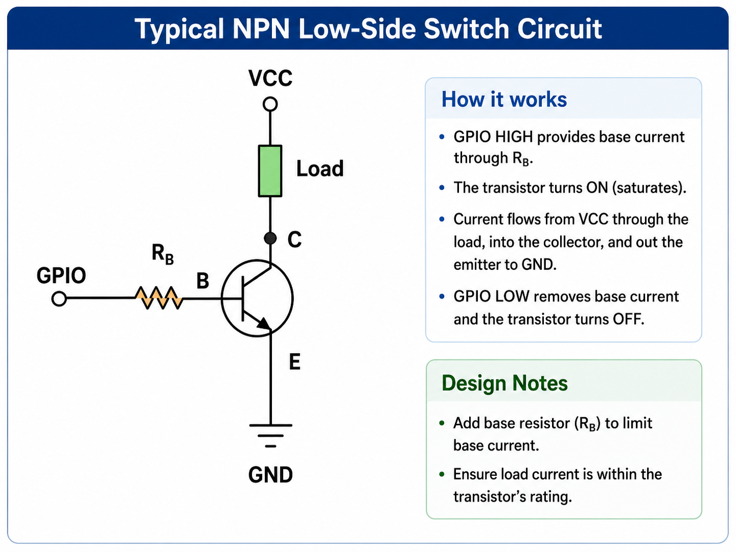
For example, an NPN transistor used as a low-side switch must have the emitter connected to the lower potential side, usually ground. If a PNP transistor symbol is used by mistake, the control logic changes. The base drive, load direction, and turn-on condition become different. The PCB may pass a visual check but fail functional testing.
How Does a Transistor Symbol Work?
A transistor symbol works by showing the terminals and control path of the transistor. The graphic structure tells the reader which terminal controls conduction and which terminals carry the main current.
For BJT symbols, the base controls current between the collector and emitter. The small arrow is placed on the emitter. In an NPN transistor symbol, the arrow points outward. In a PNP transistor symbol, the arrow points inward.
For MOSFET and JFET symbols, the gate controls the channel between drain and source. A MOSFET symbol often shows an insulated gate structure, while a JFET symbol shows a junction-controlled gate.
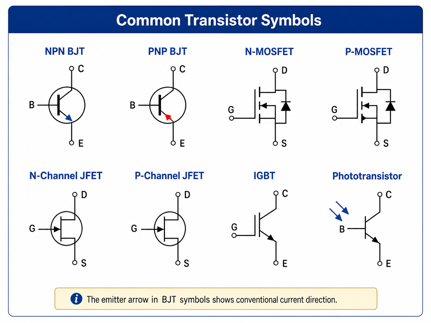
Main Types of Transistor Symbols
The most common transistor symbols are BJT, MOSFET, JFET, IGBT, Darlington transistor, and phototransistor symbols. Each type has a different control method and a different use case.
| Transistor Type | Common Symbol Terminals | Common Use | Key Symbol Feature |
|---|---|---|---|
| NPN BJT | Collector, Base, Emitter | Low-side switching, signal amplification | Emitter arrow points out |
| PNP BJT | Collector, Base, Emitter | High-side switching, complementary circuits | Emitter arrow points in |
| N-channel MOSFET | Drain, Gate, Source | Power switching, motor control, LED drivers | Gate separated from channel |
| P-channel MOSFET | Drain, Gate, Source | High-side switching, reverse protection | P-channel direction marking |
| JFET | Drain, Gate, Source | Low-noise analog circuits, input stages | Gate forms a junction with channel |
| IGBT | Collector, Gate, Emitter | High-voltage power switching | MOS gate with bipolar output path |
| Darlington transistor | Collector, Base, Emitter | High-gain switching | Two-transistor combined symbol |
| Phototransistor | Collector, Emitter, sometimes Base | Optical sensing | Light arrows point toward transistor |
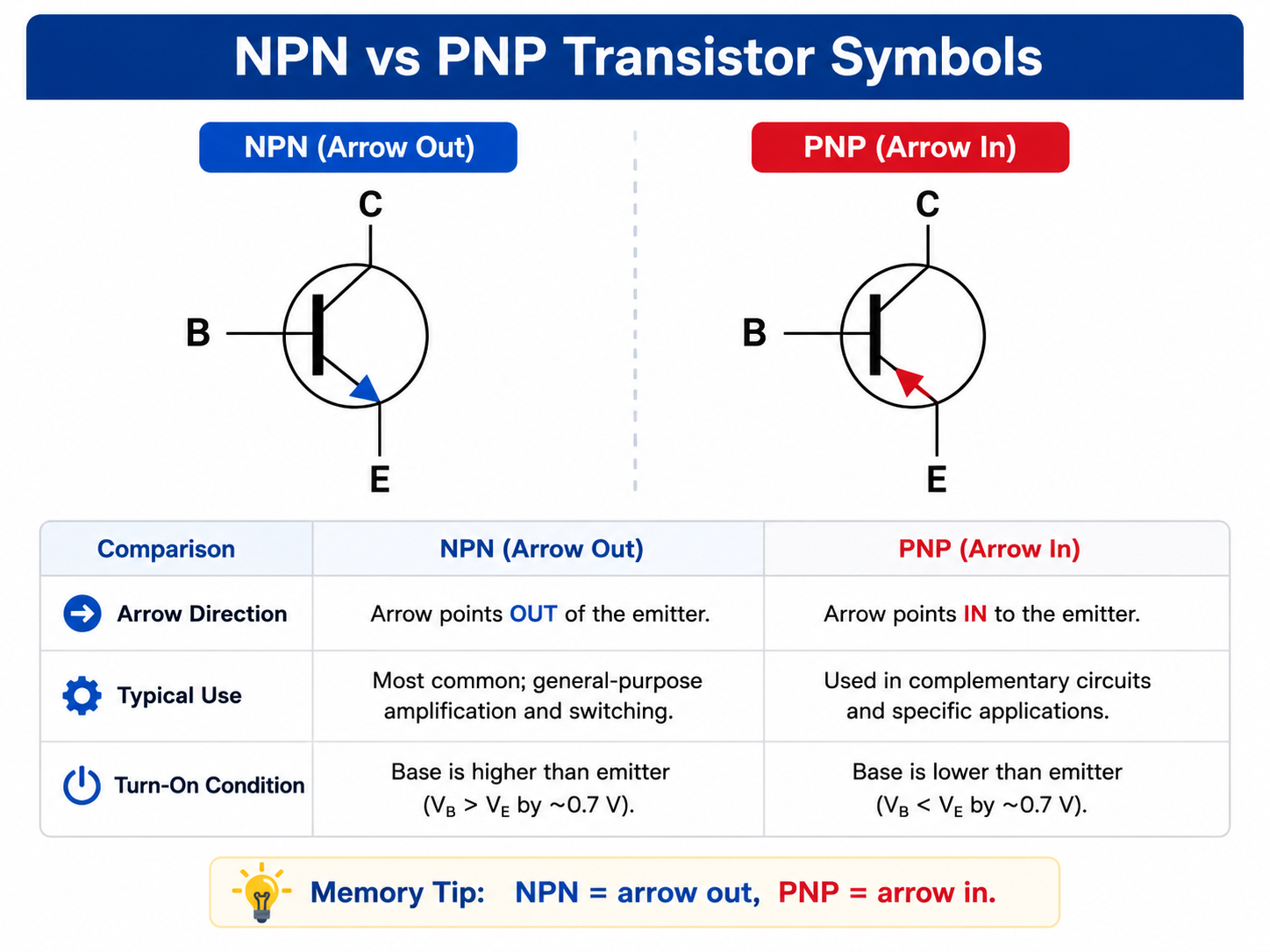
NPN Transistor Symbol vs PNP Transistor Symbol
The fastest way to identify NPN and PNP transistor symbols is to look at the emitter arrow. NPN points out. PNP points in.
| Feature | NPN Transistor Symbol | PNP Transistor Symbol |
|---|---|---|
| Arrow direction | Outward from emitter | Inward toward emitter |
| Common switching position | Low-side switch | High-side switch |
| Typical turn-on condition | Base higher than emitter | Base lower than emitter |
| Common load path | Load to supply, transistor to ground | Transistor near supply side |
| Common beginner mistake | Reversing collector and emitter | Driving base with wrong polarity |
A practical memory aid is: NPN = Not Pointing iN. The arrow points away from the base. PNP points toward the base.
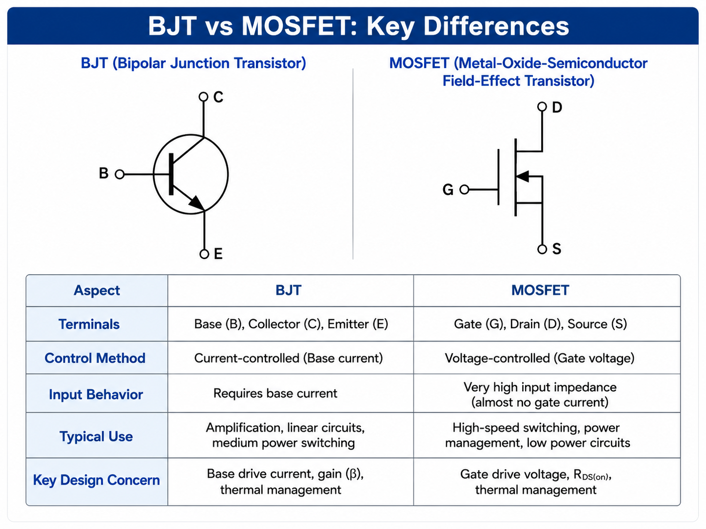
MOSFET Symbol vs BJT Symbol
A MOSFET symbol is different from a BJT symbol because a MOSFET is voltage-controlled, while a BJT is current-controlled. In a BJT, the base current controls collector-emitter current. In a MOSFET, the gate voltage controls the drain-source channel.
| Item | BJT Symbol | MOSFET Symbol |
|---|---|---|
| Terminals | Collector, Base, Emitter | Drain, Gate, Source |
| Control method | Base current | Gate-source voltage |
| Input behavior | Requires base current | Very high input impedance |
| Common PCB use | Signal switching, simple drivers | Power switching, load control, DC-DC converters |
| Typical design concern | Base resistor, gain variation | Gate drive, body diode, VGS limit |
| Symbol risk | NPN/PNP confusion | Drain/source/body diode confusion |
MOSFET symbols may show enhancement or depletion mode. Depletion MOSFET symbols usually indicate a normally conductive channel, while enhancement-mode MOSFETs are normally off and are much more common in digital switching and power control.
What Materials Are Used in Transistors?
Most common transistors use silicon as the semiconductor material, but advanced applications may use silicon carbide, gallium nitride, or other semiconductor materials. The symbol usually does not show the material, so the datasheet must provide that information.
| Material | Common Devices | Typical Strength | Common Application |
|---|---|---|---|
| Silicon | BJT, MOSFET, small-signal transistor | Mature, cost-effective, widely available | Consumer, industrial, communication, control boards |
| Silicon carbide | SiC MOSFET, SiC diode modules | High voltage, high temperature, high efficiency | EV, solar inverter, industrial power |
| Gallium nitride | GaN FET | Fast switching, high power density | Chargers, RF, high-frequency power |
| Germanium | Older transistor types | Low forward voltage, historical use | Vintage audio, legacy repair |
For most PCB projects, the main issue is not the semiconductor material itself. The more urgent questions are package type, voltage rating, current rating, thermal path, availability, and assembly compatibility.
Transistor Symbol Standards and Schematic Conventions
Transistor symbols are commonly based on established diagram conventions such as IEC 60617 and IEEE/ANSI-style schematic practices. In PCB projects, the standard symbol is only one part of the library system.
| Library Item | Purpose | Common Risk |
|---|---|---|
| Schematic symbol | Shows electrical function | Wrong terminal naming |
| PCB footprint | Defines copper pads and package outline | Wrong pad size or pin order |
| 3D model | Checks mechanical clearance | Height or body mismatch |
| BOM data | Defines manufacturer part number | Wrong substitute part |
| Pick-and-place data | Guides SMT placement | Rotation or origin error |
| Assembly drawing | Helps inspection | Missing polarity or orientation note |
A reliable symbol library saves time during engineering review. It also reduces avoidable communication problems between design teams and PCB assembly suppliers.
How to Read a Transistor Symbol on a PCB Schematic?
To read a transistor symbol correctly, start with the terminal names, then identify the transistor type, arrow direction, control pin, and connected circuit function.
| Step | What to Check | Engineering Reason |
|---|---|---|
| Check the reference designator | Usually Q or sometimes T | Confirms it is a transistor-type component |
| Identify the type | BJT, MOSFET, JFET, IGBT | Determines control method |
| Read terminal names | C/B/E or D/G/S | Prevents wrong net connection |
| Check arrow direction | NPN, PNP, channel indication | Confirms polarity and current logic |
| Review nearby resistors | Base resistor, gate resistor, pull-down | Confirms drive stability |
| Check load position | High-side or low-side | Confirms switching topology |
| Compare with datasheet | Pinout, ratings, package | Prevents symbol-footprint mismatch |
| Verify PCB footprint | Pad order and land pattern | Prevents assembly failure |
A transistor symbol should never be reviewed in isolation. The symbol, component value, manufacturer part number, footprint, and circuit context must be checked together.
Transistor Symbol vs Transistor Footprint
A transistor symbol shows electrical function, while a footprint shows the physical solder pad layout on the PCB. Confusing the two is one of the most common mistakes in hardware design.
| Item | Transistor Symbol | Transistor Footprint |
|---|---|---|
| Used in | Schematic | PCB layout |
| Shows | Electrical pins and function | Copper pads, body outline, courtyard |
| Example | NPN BJT symbol | SOT-23, TO-92, SOT-223, DPAK |
| Main risk | Wrong circuit interpretation | Wrong assembly or pin connection |
| Checked by | Schematic review, ERC | DRC, footprint review, assembly drawing |
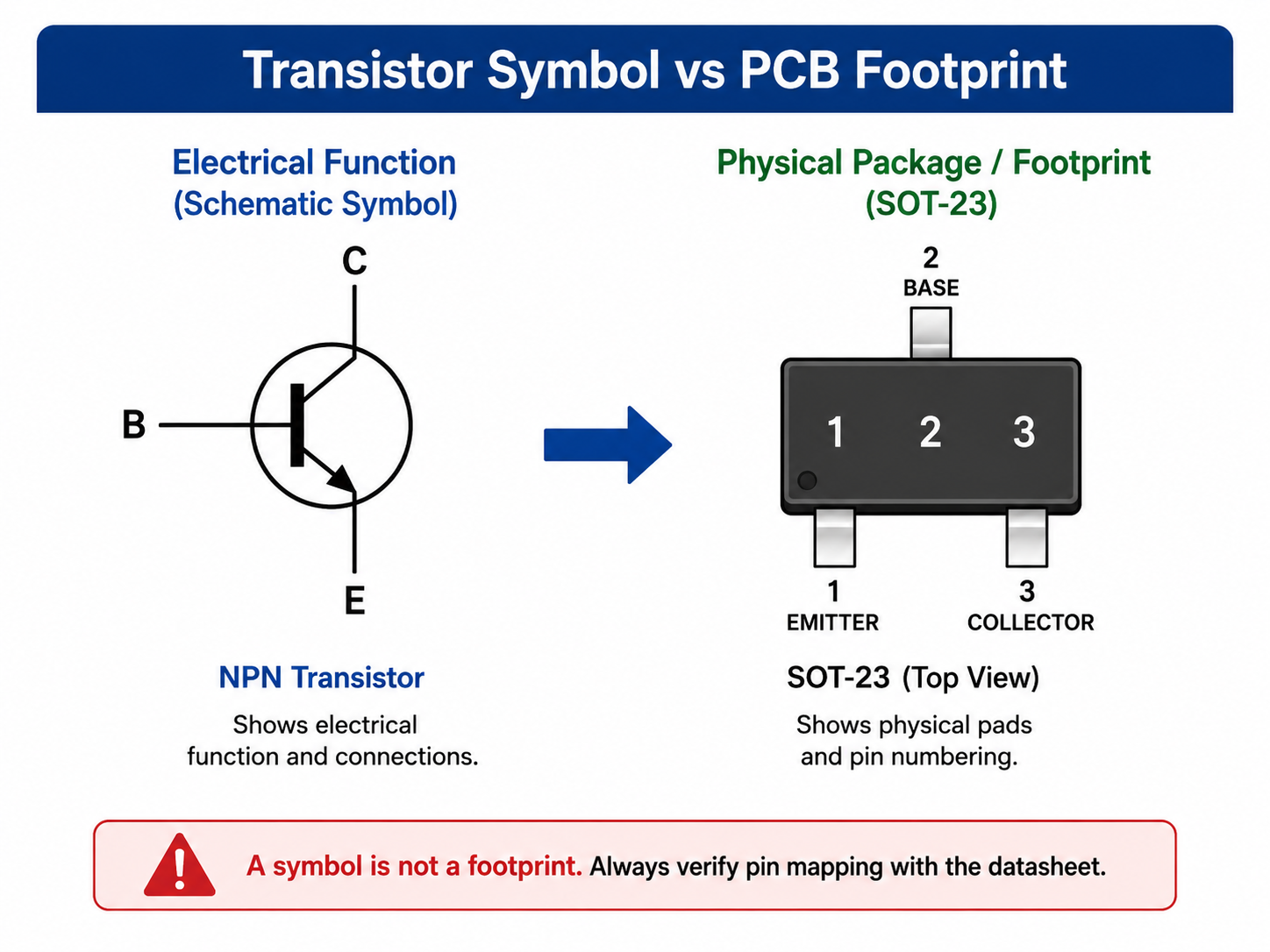
The transistor symbol may be electrically correct, but the PCB can still fail if the footprint is wrong. A SOT-23 transistor footprint may look simple, but pin 1, pin 2, and pin 3 must match the selected part.
How to Choose the Right Transistor Symbol for Your Circuit?
Choose the transistor symbol based on the actual transistor type, control method, circuit position, and manufacturer part number. Do not select a symbol only because it looks familiar.
| Design Need | Better Symbol Choice | Key Check |
|---|---|---|
| Simple low-side load switch | NPN BJT or N-channel MOSFET | Load current and drive level |
| High-side switch | PNP BJT or P-channel MOSFET | Gate/base drive voltage |
| Fast digital switching | MOSFET | Gate charge and switching loss |
| Small-signal amplification | BJT or JFET | Bias point and noise level |
| High-voltage power control | MOSFET or IGBT | Voltage rating, creepage, thermal path |
| Optical sensing | Phototransistor | Light direction and response time |
| High gain with simple drive | Darlington transistor | Saturation voltage and heat |
For production boards, the symbol should include clear pin names, package link, manufacturer part number, and verified footprint mapping. Generic symbols are acceptable for early discussion, but they should be replaced or fully defined before quotation, PCB fabrication, and assembly.
Common Transistor Symbol Mistakes in PCB Design
Most transistor symbol mistakes are small on the screen but expensive after assembly. They often appear during prototype bring-up, when the board does not switch, the output is inverted, or the transistor overheats.
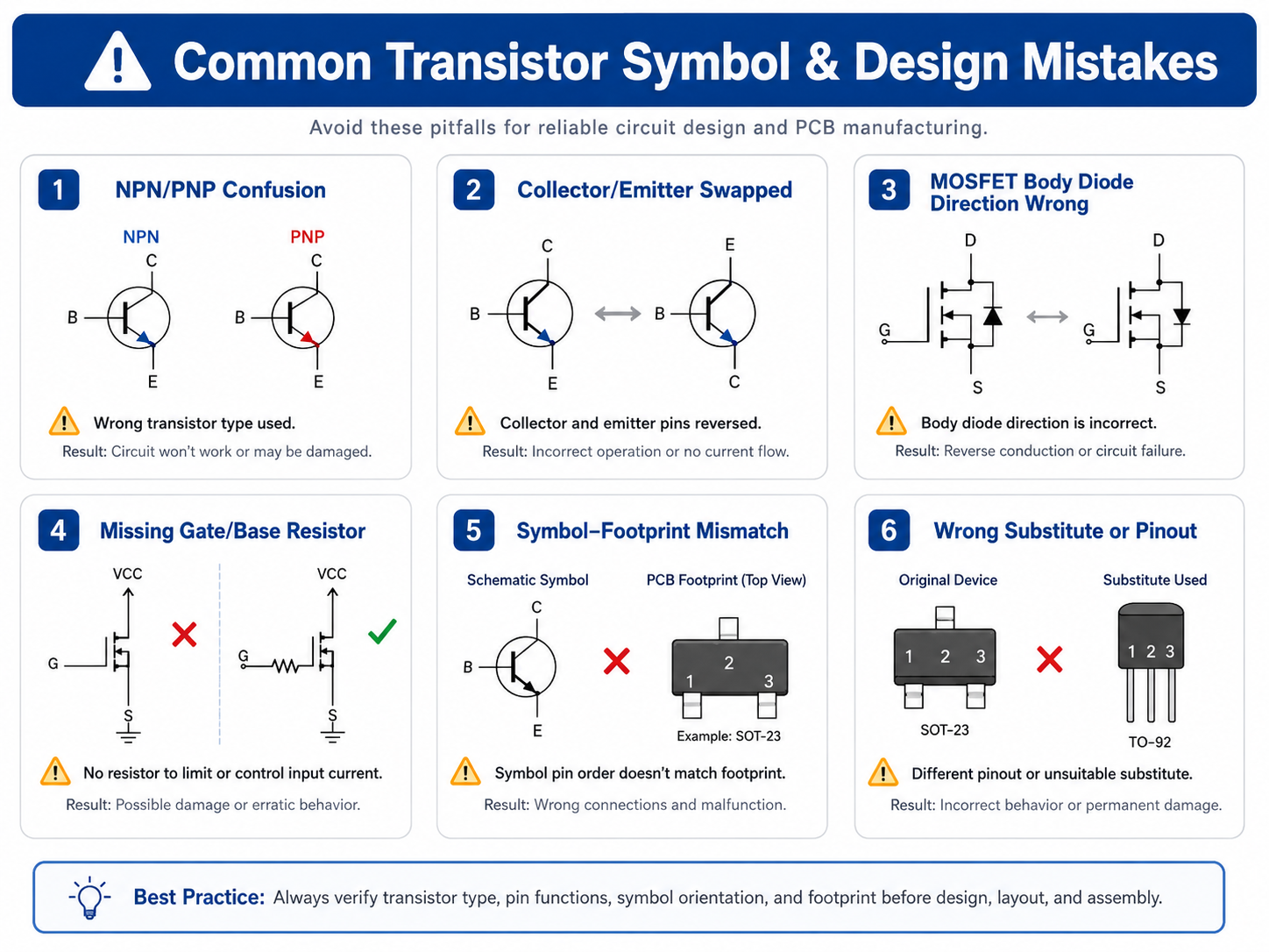
A useful factory-side check is to compare the schematic symbol, footprint, BOM, and pick-and-place file before production. This review is especially valuable for small SOT-23, SOT-223, DPAK, DFN, and QFN transistor packages.
Transistor Symbol in PCB Manufacturing and PCBA Assembly
In PCB manufacturing and PCBA assembly, the transistor symbol becomes part of a larger production data chain. It starts in the schematic, moves into the PCB layout, appears in the BOM, and finally reaches SMT placement and inspection.
| Stage | File or Data | Transistor-Related Check |
|---|---|---|
| Schematic design | Circuit schematic | Correct symbol and pin names |
| PCB layout | Gerber and CAD data | Footprint and copper thermal path |
| BOM review | Manufacturer part number | Correct transistor type and package |
| Sourcing | Approved supplier list | Availability and substitute control |
| SMT programming | Pick-and-place file | Rotation, pin 1, centroid |
| Assembly inspection | AOI, visual inspection | Orientation and solder quality |
| Electrical test | ICT or functional test | Switching, gain, leakage, voltage drop |
For transistor-heavy boards, quality control should not stop at solder appearance. Functional behavior must also be checked because a transistor can look correctly soldered but still be electrically wrong due to symbol, footprint, or BOM mismatch.
Testing Methods for Transistor Symbol and Circuit Accuracy
The transistor symbol itself is not tested with lab equipment, but the circuit built from that symbol can and should be verified. Testing should begin before PCB fabrication and continue through assembly and functional validation.
| Test Method | When Used | What It Finds |
|---|---|---|
| ERC check | Schematic stage | Floating base/gate, missing connections |
| CAD library audit | Before layout release | Symbol-footprint mismatch |
| DRC check | PCB layout stage | Clearance, copper, pad, and routing issues |
| BOM review | Before sourcing | Wrong transistor type or package |
| Multimeter diode test | Debug stage | BJT junction behavior and pin identification |
| Oscilloscope test | Functional test | Switching waveform, ringing, delay |
| Thermal camera | Load test | Hot transistor or weak copper area |
| AOI/visual inspection | Assembly stage | Orientation and solder defects |
| X-ray inspection | Hidden joints or advanced packages | Void, bridge, or hidden solder issue |
For small BJT circuits, a multimeter diode mode can help confirm base-emitter and base-collector junctions. For MOSFET circuits, check gate-source voltage, drain-source voltage, body diode direction, and gate pull-down behavior. For power circuits, thermal testing under realistic load is essential.
Quality Standards and Documentation for Transistor-Based PCB Projects
A transistor-based PCB project needs more than a correct schematic. It needs controlled documentation so the manufacturer can build the same board repeatedly.
| Document | Why It Matters |
|---|---|
| Schematic PDF | Shows intended circuit function and transistor symbols |
| Gerber files | Defines copper, solder mask, silkscreen, and fabrication data |
| BOM with MPN | Prevents wrong transistor sourcing |
| Pick-and-place file | Controls SMT placement and rotation |
| Assembly drawing | Shows component orientation and special notes |
| Approved substitute list | Controls alternates without changing circuit behavior |
| Test plan | Defines switching, voltage, current, and functional checks |
| Quality requirement | Defines IPC class, inspection criteria, and acceptance level |
For overseas procurement, clear documentation reduces back-and-forth communication. It also prevents a common problem: the purchasing team buys a transistor with the same package and similar rating, but with a different pinout or switching behavior.
Industry Applications of Transistor Symbols and Transistor Circuits
Transistor symbols appear in nearly every electronic industry because transistors are core building blocks in modern circuits. The symbol helps engineers understand how control, switching, amplification, and protection are implemented.
| Industry | Typical Transistor Use | PCB Design Concern |
|---|---|---|
| Consumer electronics | Signal switching, charging, display control | Compact layout and cost control |
| Automotive electronics | Load switching, sensor interface, motor control | Reliability, thermal cycling, vibration |
| Industrial control | Relay drivers, PLC I/O, isolation circuits | Surge protection and long service life |
| Medical electronics | Signal conditioning, sensor circuits | Stability, traceability, clean assembly |
| LED lighting | Constant-current control, dimming | Thermal management and current handling |
| Communication devices | RF switching, bias circuits, amplification | Noise control and impedance behavior |
| Power electronics | MOSFET and IGBT switching | Creepage, heat, copper thickness |
| Smart home devices | Low-power switching and interface circuits | Standby power and compact PCBA |
In high-reliability industries, the transistor symbol is not just a drawing. It is part of design traceability. Engineers must know why a transistor was selected, how it is driven, what failure mode is expected, and whether the PCB layout supports the electrical and thermal requirement.
FAQs About Transistor Symbols
Q1: What does a transistor symbol mean?
A transistor symbol represents the electrical function of a transistor in a schematic. It shows the transistor type and terminals, such as collector, base, and emitter for BJT devices or drain, gate, and source for FET devices. The symbol helps engineers understand control direction, current path, and circuit behavior before the PCB is designed or assembled.
Q2: How can I identify an NPN transistor symbol?
An NPN transistor symbol has an arrow on the emitter pointing outward. The arrow direction shows conventional current direction at the emitter. In many low-side switching circuits, the emitter connects toward ground, the collector connects to the load, and the base receives the control signal through a resistor. Always confirm the physical pinout with the datasheet.
Q3: How can I identify a PNP transistor symbol?
A PNP transistor symbol has an arrow on the emitter pointing inward. PNP transistors are often used in high-side switching or complementary circuits. They usually turn on when the base is pulled lower than the emitter. The symbol helps identify the bias direction, but the package pinout still needs datasheet verification before PCB layout.
Q4: What is the difference between a BJT symbol and a MOSFET symbol?
A BJT symbol uses collector, base, and emitter terminals, while a MOSFET symbol uses drain, gate, and source terminals. A BJT is controlled by base current. A MOSFET is controlled by gate-source voltage. In PCB design, MOSFET symbols also require careful attention to body diode direction, gate drive voltage, and thermal dissipation.
Q5: What does the arrow mean in a transistor symbol?
The arrow usually shows conventional current direction and helps identify transistor type. In a BJT symbol, the arrow is placed on the emitter. NPN points outward, while PNP points inward. In FET symbols, arrow direction may indicate channel type or junction direction, depending on the symbol convention used in the schematic library.
Q6: Is the transistor symbol the same as the transistor footprint?
No. The transistor symbol is used in the schematic to show electrical function. The footprint is used in PCB layout to show pad shape, pad spacing, and component body position. A design can have a correct symbol but a wrong footprint. That mismatch can cause assembly failure even when the circuit idea is correct.
Q7: Why do transistor pinouts differ between similar packages?
Package appearance does not guarantee the same pin order. Two SOT-23 or TO-92 transistors may have different internal pin arrangements depending on manufacturer and part number. This is why engineers must verify the datasheet, symbol-to-footprint mapping, and BOM before releasing PCB files for fabrication and assembly.
Q8: What is the common reference designator for a transistor?
The common reference designator for a transistor is usually Q, such as Q1, Q2, or Q15. Some older drawings may use other letters, but Q is widely recognized in PCB schematics. A clear reference designator helps connect schematic symbols, BOM lines, PCB footprints, assembly drawings, and inspection records.
Q9: Can I use a generic transistor symbol in my schematic?
A generic symbol can be used during early concept design, but production schematics should define the exact transistor type, pin names, package, and manufacturer part number. Generic symbols increase the risk of wrong pin mapping, wrong package selection, and sourcing mistakes. For PCBA production, a controlled library is much safer.
Q10: What causes a transistor circuit to fail after PCB assembly?
Common causes include wrong NPN/PNP selection, incorrect MOSFET drain-source direction, symbol-footprint mismatch, missing gate or base resistor, floating gate, wrong substitute part, insufficient copper for heat dissipation, or incorrect assembly orientation. A complete review should compare the schematic, datasheet, BOM, footprint, pick-and-place file, and functional test result.
Conclusion
A transistor symbol is small, but it carries critical design information. It identifies the transistor type, terminal function, current direction, control method, and circuit behavior. For reliable PCB and PCBA production, the symbol must match the datasheet, footprint, BOM, assembly orientation, and test plan.
If you are sourcing reliable PCB/PCBA manufacturing, including OEM, ODM, prototyping, mass production, or custom engineering solutions, reach out to our engineering team for technical support and a quote at sales@bestpcbs.com.