PCB manufacturing PCB manufacturing
Home > Blog

npn transistor symbol

Transistor Symbol, Pinout, Meaning, Types & PCB Use
Thursday, July 2nd, 2026

A transistor is one of the most important components in modern electronics. It can switch current, amplify signals, regulate power, drive loads, and form the basic building block of digital circuits. From small sensor modules to industrial control boards, power supplies, audio circuits, LED drivers, communication devices, and embedded systems, transistors appear almost everywhere.

This guide explains the transistor symbol, transistor symbol in PCB documentation, transistor symbol pinout, arrow meaning, NPN and PNP types, MOSFET and BJT symbols, switching use, voltage requirements, testing methods, common applications, and failure behavior.
Transistor Symbol, Pinout, Meaning, Types & PCB Use

What Is the Symbol for a Transistor?

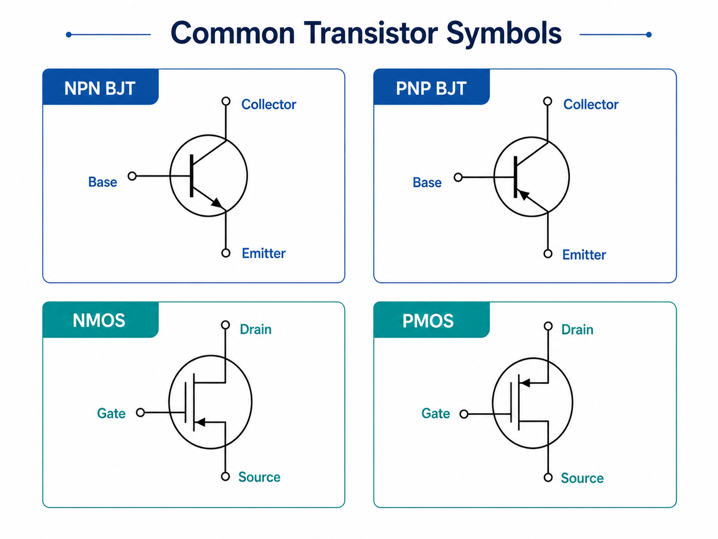
A transistor symbol is the schematic representation of a transistor in an electronic circuit diagram. It helps engineers understand how the transistor is connected and how current flows through the circuit.

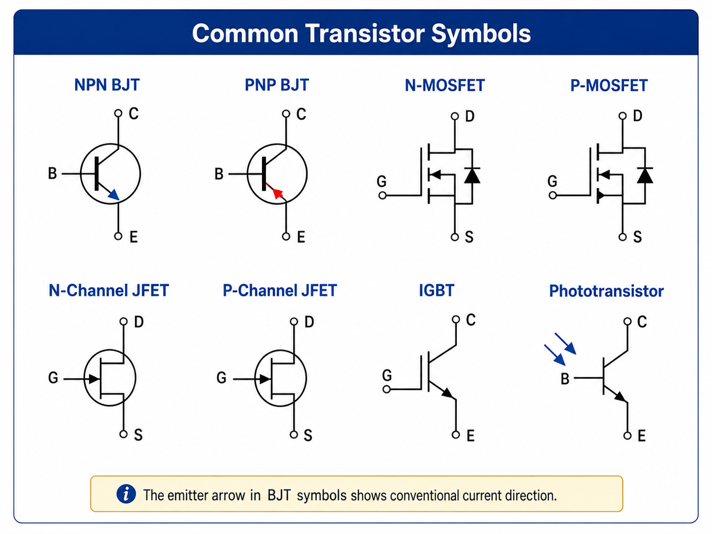
The most common transistor symbols are used for BJT transistors and MOSFET transistors.

A BJT transistor symbol usually has three terminals:

TerminalFull NameMain Function
BBaseControls the transistor
CCollectorReceives or supplies main current
EEmitterCurrent output or reference terminal

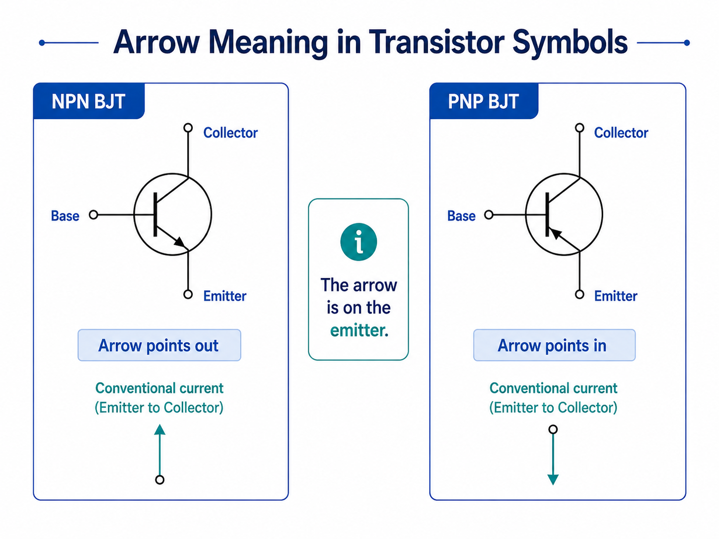
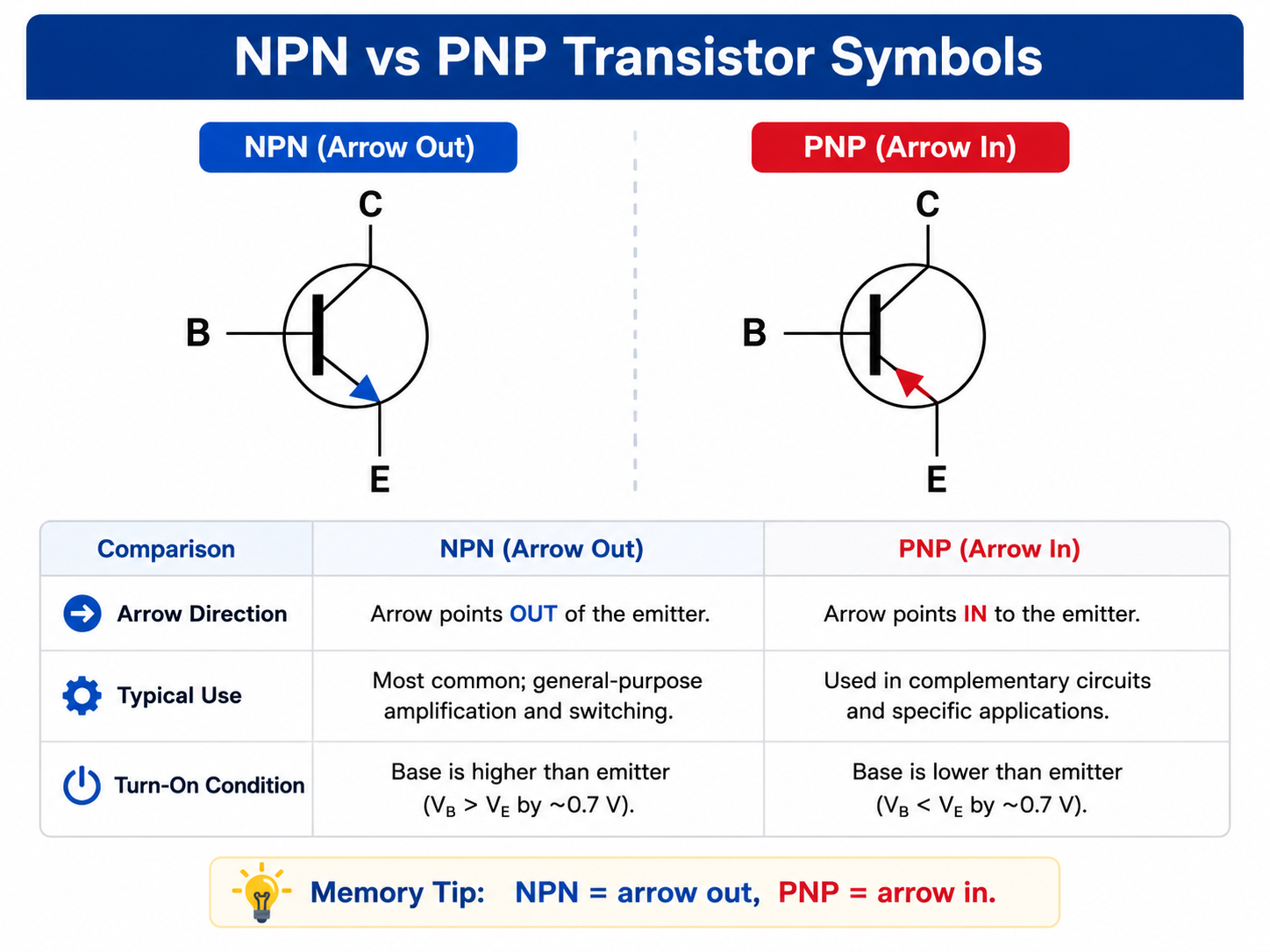
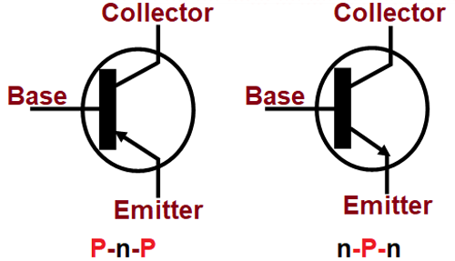
In an NPN or PNP BJT symbol, the arrow is placed on the emitter. The arrow direction helps identify whether the transistor is NPN or PNP.

A MOSFET transistor symbol also has three main terminals:

TerminalFull NameMain Function
GGateControls conduction by voltage
DDrainMain current terminal
SSourceMain current terminal or reference

Some MOSFET symbols also show the body diode, substrate, or enhancement/depletion mode structure.

In simple terms, a transistor symbol tells you three things: what type of transistor it is, where each pin connects, and how the device controls current.

Transistor Symbol in PCB

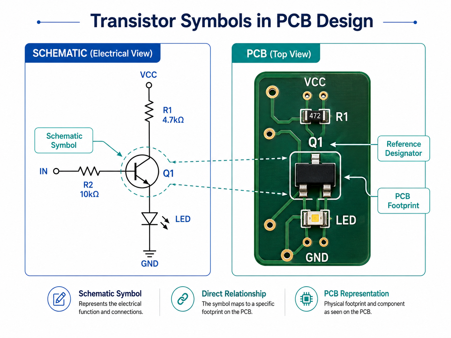
A transistor symbol in PCB work can appear in several places. It is usually seen in the schematic, component library, datasheet, silkscreen reference, and PCB assembly drawing.

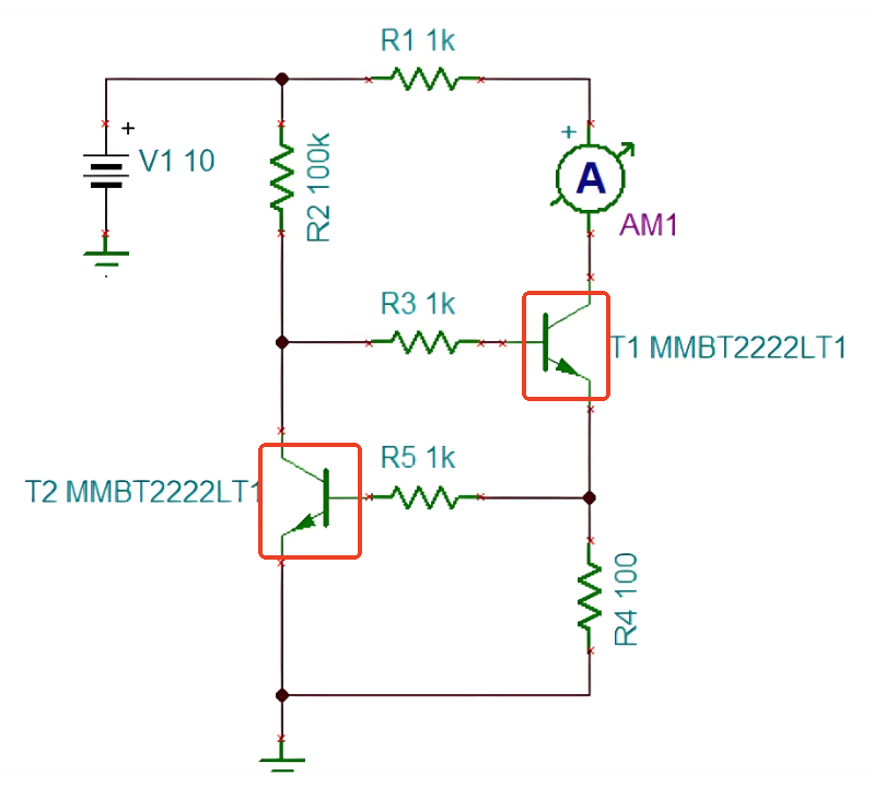
In a schematic, the transistor symbol shows the electrical function. For example, it may show whether the device is an NPN transistor used as a low-side switch, a PNP transistor used as a high-side switch, an NMOS transistor used for power control, or a PMOS transistor used for reverse polarity protection.

On the actual PCB, the symbol may not be drawn in full. Instead, the PCB normally uses a reference designator, such as Q1, Q2, Q3, or Q101. The letter “Q” is commonly used to identify transistors and transistor-like semiconductor devices.

PCB silkscreen may also show a small outline of the package. Common transistor packages include SOT-23, SOT-223, TO-92, TO-220, TO-252, TO-263, DFN, and QFN. The PCB footprint must match the actual component package and pin arrangement.
Transistor Symbol in PCB

Transistor Symbol Pinout

Transistor symbol pinout means the relationship between the schematic terminals and the physical pins of the transistor package. This is one of the most common sources of PCB design and repair mistakes.

For a BJT, the three pins are base, collector, and emitter. In the schematic symbol, these are easy to identify. However, on the physical part, the pin order depends on the package and manufacturer.

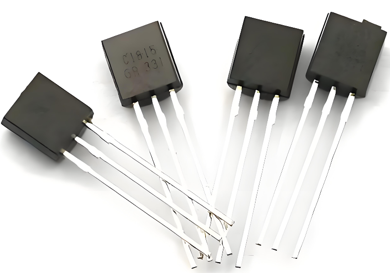
For example, a TO-92 transistor may have one of several pin arrangements, such as E-B-C, C-B-E, or E-C-B. A SOT-23 transistor may also vary depending on the exact part number.

For a MOSFET, the three pins are gate, drain, and source. In power packages such as TO-220 or DPAK, the tab is often connected to the drain, but this is not universal for every device type. Datasheet verification is still required.

Transistor Symbol Pinout

What Are the Three Pins of a Transistor Called?

The three pins of a transistor depend on the transistor type.

For a BJT, the three pins are:

Base: The control pin. A small current applied to the base controls a larger current between collector and emitter.

Collector: The main current input terminal in many NPN circuits. It is usually connected to the load or supply side.

Emitter: The terminal where current leaves the transistor in a typical NPN configuration. It is often connected to ground in low-side switching circuits.

For a MOSFET, the three pins are:

Gate: The control pin. It uses voltage, rather than base current, to control the transistor.

Drain: One of the main current terminals. In an NMOS low-side switch, the drain is often connected to the load.

Source: The other main current terminal. In an NMOS low-side switch, the source is often connected to ground.

Although both BJTs and MOSFETs have three terminals, they are controlled differently. A BJT is current-controlled, while a MOSFET is voltage-controlled. This difference affects circuit design, driver selection, power loss, and switching speed.

What Is the Significance of Arrow in the Transistor Symbol?

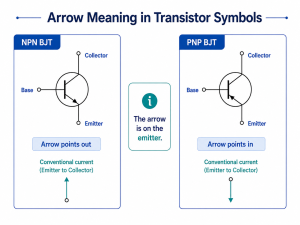
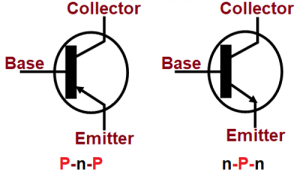
The arrow in a transistor symbol is very important. In a BJT symbol, the arrow is placed on the emitter and shows the direction of conventional current flow.

For an NPN transistor, the arrow points outward from the emitter. A simple way to remember this is: NPN means Not Pointing iN.

For a PNP transistor, the arrow points inward toward the base. This means the current direction is different from an NPN transistor.

TypeArrow DirectionBasic Meaning
NPNArrow points outCurrent flows from collector to emitter when turned on
PNPArrow points inCurrent flows from emitter to collector when turned on
What Is the Significance of Arrow in the Transistor Symbol?

The arrow also helps technicians identify transistor polarity in a schematic. This matters when replacing components, testing circuits, or checking switching paths.

What Are the Two Major Types of Transistors?

The two major types of transistors are BJT and FET.

BJT stands for Bipolar Junction Transistor. It uses both electrons and holes for conduction. BJT devices are commonly used for signal amplification, switching, audio circuits, and general-purpose control circuits. The two main BJT types are NPN and PNP.

FET stands for Field-Effect Transistor. It controls current through an electric field. The most common FET used in PCB design is the MOSFET, which stands for Metal-Oxide-Semiconductor Field-Effect Transistor. MOSFETs are widely used in power switching, motor drivers, battery protection circuits, DC-DC converters, and logic-level control circuits.

CategoryMain TypesControl MethodCommon Use
BJTNPN, PNPBase currentAmplification and small-signal switching
FETNMOS, PMOS, JFETGate voltagePower switching and high-input impedance circuits

In modern PCB design, MOSFETs are very common because they can switch efficiently, handle high current, and work well with microcontroller outputs when properly selected. BJTs are still widely used where simple biasing, low cost, linear gain, or predictable small-signal behavior is needed.

Why Are Transistors Called NPN or PNP?

NPN and PNP names describe the semiconductor layer structure inside a BJT.

An NPN transistor has a thin P-type region between two N-type regions. The three regions form the collector, base, and emitter. In many low-voltage electronic circuits, NPN transistors are used as low-side switches because they are easy to drive from microcontrollers or logic circuits.

A PNP transistor has a thin N-type region between two P-type regions. PNP transistors are often used for high-side switching, signal control, and complementary amplifier circuits.

TypeInternal StructureCommon Switching Position
NPNN-P-NLow-side switching
PNPP-N-PHigh-side switching

The naming is not just theoretical. It directly affects how the transistor is biased. An NPN transistor turns on when the base is at a higher voltage than the emitter by about 0.6–0.7 V for silicon devices. A PNP transistor turns on when the base is lower than the emitter by about 0.6–0.7 V.

This difference is why NPN and PNP transistor symbols must not be confused. Replacing one with the other will usually make the circuit fail or behave incorrectly.

Can I Use an NPN Transistor as a Switch?

Yes, an NPN transistor can be used as a switch. This is one of the most common uses of an NPN transistor in PCB circuits.

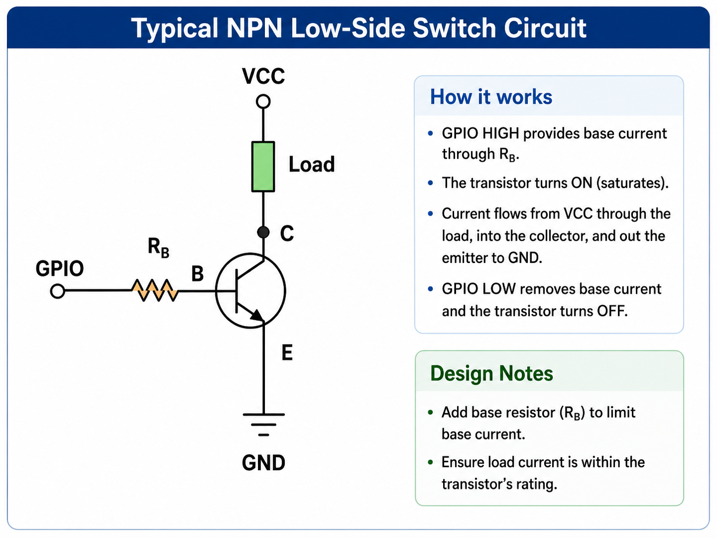
A typical NPN switching circuit works as a low-side switch. The load is connected between the positive supply and the collector. The emitter is connected to ground. When enough base current flows, the transistor turns on and allows current to pass from collector to emitter.

Common loads controlled by NPN transistor switches include LEDs, relays, buzzers, small motors, optocouplers, and signal lines.

A basic NPN switching circuit normally needs:

PartPurpose
NPN transistorControls the load
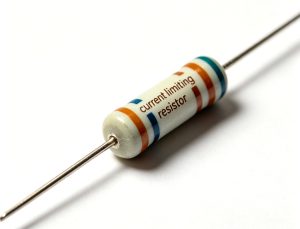
Base resistorLimits base current
LoadLED, relay, buzzer, or other device
Flyback diodeProtects transistor when driving inductive loads
Pull-down resistorKeeps transistor off when input is floating

For relay and motor circuits, a flyback diode is especially important. Without it, voltage spikes from the coil may damage the transistor.

When using an NPN transistor as a switch, the designer must check collector current, collector-emitter voltage, base current, power dissipation, saturation voltage, package thermal performance, and PCB copper area. For high-current switching, a logic-level NMOS transistor may be a better choice because it usually has lower conduction loss.

How Much Voltage Does a Transistor Need?

The voltage a transistor needs depends on its type and how it is used.

For a silicon BJT, the base-emitter junction usually starts conducting at about 0.6–0.7 V. However, this does not mean every BJT circuit only needs 0.7 V. The full circuit must provide enough voltage and current to drive the load.

For a BJT used as a switch, the base must receive enough current to drive the transistor into saturation. The base resistor must be calculated based on input voltage, base-emitter voltage, load current, and required gain margin.

For a MOSFET, the gate voltage controls conduction. A MOSFET has a parameter called gate threshold voltage, often written as VGS(th). However, this value only indicates when the MOSFET starts to conduct a very small current. It does not mean the MOSFET is fully on.

For practical switching, designers should check the MOSFET’s RDS(on) at the actual gate drive voltage. For example, if a microcontroller outputs 3.3 V, the MOSFET should have a low RDS(on) specified at 2.5 V or 3.3 V, not only at 10 V.

Transistor TypeControl RequirementDesign Note
BJTBase-emitter voltage plus base currentNeeds a base resistor
NMOSGate-source voltageCheck RDS(on) at real drive voltage
PMOSGate-source voltage, usually negative relative to sourceOften used in high-side circuits

Voltage selection should always consider the supply voltage, signal level, load current, temperature, and safety margin.

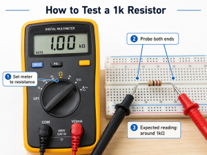
How Do You Test If a Transistor Is Working?

A transistor can be tested with a multimeter, component tester, or circuit-level measurement. The best method depends on whether the transistor is removed from the PCB or still soldered on the board.

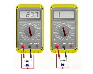
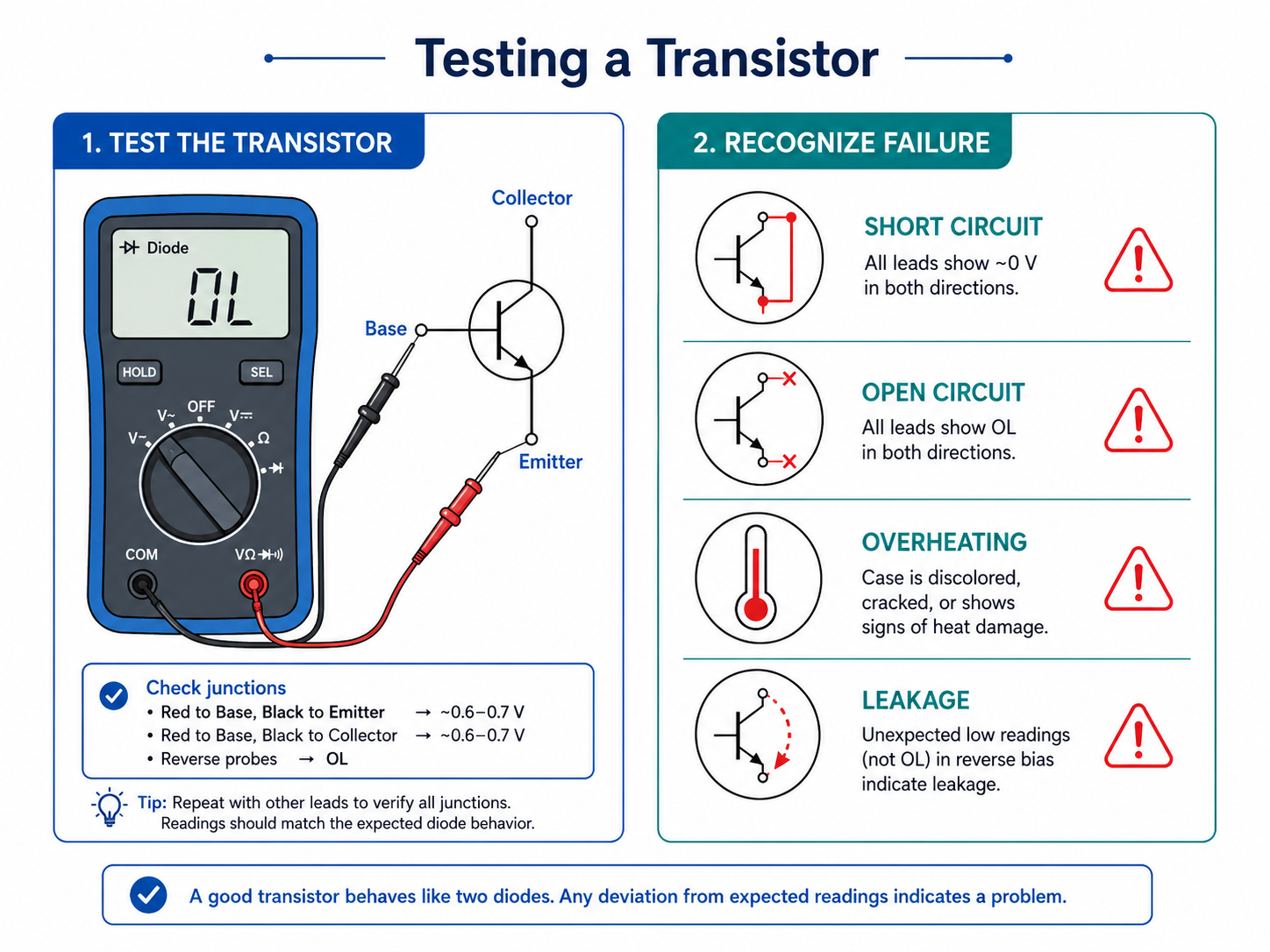
For a BJT, a digital multimeter in diode mode can check the base-emitter and base-collector junctions. An NPN transistor behaves like two diodes sharing the base. A normal silicon junction often shows a forward voltage drop around 0.6–0.7 V. A PNP transistor is tested with reversed probe polarity.

Basic BJT test signs:
How Do You Test If a Transistor Is Working?

For a MOSFET, testing is different. A multimeter can check for drain-source shorts and body diode behavior. Some MOSFETs can also be briefly charged at the gate to see if the channel turns on, but this method must be used carefully because MOSFET gates can be damaged by static electricity.

When the transistor is still on a PCB, surrounding components may affect readings. Resistors, diodes, IC pins, coils, or capacitors connected to the same circuit can create misleading results. If the measurement is unclear, lifting one pin or removing the transistor gives a more reliable test.

In production PCB assembly, transistor testing may also include AOI, X-ray for hidden joints, in-circuit testing, functional testing, and thermal inspection under load.

What Is a Transistor Used For?

A transistor is used to control electrical current. Its two major functions are switching and amplification.

In switching circuits, a transistor works like an electronic on/off control. It can allow a low-power signal from a microcontroller to control a larger load. This is common in LED control, relay drivers, motor drivers, power enable circuits, battery management systems, and digital output stages.

In amplification circuits, a transistor increases the strength of a small signal. This is used in audio amplifiers, RF circuits, sensor interfaces, analog front ends, and signal conditioning circuits.

Common transistor applications include:

ApplicationTypical Transistor Role
LED driverControls LED current
Relay driverSwitches relay coil current
Audio amplifierAmplifies weak audio signals
Power supplySupports regulation and switching
Motor controlDrives or modulates motor current
Battery circuitProvides protection or switching
Logic interfaceConverts or buffers signals
RF circuitAmplifies high-frequency signals
Sensor circuitConditions small analog signals

In PCB design, transistors are often small but critical. A single wrong transistor selection may cause overheating, unstable switching, weak drive strength, leakage current, voltage drop, or signal distortion.

For this reason, engineers should select transistors based on real working conditions, not only package size or price. Important parameters include voltage rating, current rating, gain, threshold voltage, RDS(on), switching speed, leakage current, power dissipation, thermal resistance, and package availability.

What Happens When a Transistor Fails?

When a transistor fails, the circuit may stop working, work intermittently, overheat, draw too much current, or produce incorrect output signals. The exact symptom depends on the failure mode.

A transistor may fail as a short circuit, open circuit, leakage path, degraded gain, unstable switching device, or thermally damaged part.

Failure ModeCommon Symptom
Shorted collector-emitter or drain-sourceLoad stays on, fuse blows, power rail drops
Open internal junctionLoad never turns on
Excessive leakageCircuit behaves unpredictably
Reduced gainWeak switching or low amplification
Gate oxide damage in MOSFETDevice cannot switch correctly
Thermal damageBurn marks, discoloration, repeated failure

Common causes of transistor failure include overcurrent, overvoltage, electrostatic discharge, wrong pinout, poor heat dissipation, insufficient base/gate drive, inductive voltage spikes, soldering damage, and incorrect replacement parts.

On a PCB, transistor failure may also be caused by design issues. For example, a relay driver without a flyback diode can repeatedly stress the transistor. A MOSFET with insufficient gate voltage may operate in a partially on state and overheat. A BJT without a proper base resistor may draw excessive current from the control circuit.

When troubleshooting, do not only replace the failed transistor. It is better to check the load, driver signal, surrounding resistors, protection diodes, PCB solder joints, and power supply behavior. If the root cause remains, the new transistor may fail again.
You may also like

Transistor Symbol Explained: BJT, MOSFET, JFET, PCB Design, and Selection Guide
Tuesday, June 30th, 2026

A transistor symbol is the schematic graphic used to represent a transistor in an electronic circuit diagram. It tells engineers the transistor type, terminal names, current-control method, and sometimes whether the device is NPN, PNP, N-channel, P-channel, enhancement mode, or depletion mode.

For PCB design and PCBA manufacturing, reading the transistor symbol correctly is more than a classroom skill. A wrong symbol, wrong pin mapping, or wrong footprint can cause reversed polarity, failed switching, excessive heat, unstable signal behavior, or a complete board failure after assembly.

What Is a Transistor Symbol?

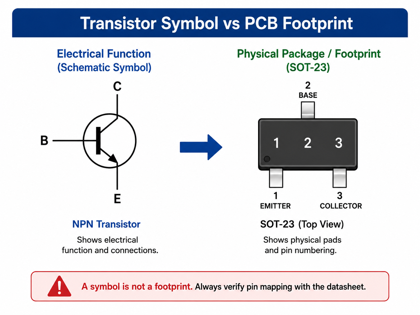
A transistor symbol is a standardized drawing used in schematics to show how a transistor connects and functions inside a circuit. It does not show the physical package. Instead, it shows the electrical role of the device.

A transistor normally has three terminals. In a BJT, these terminals are collector, base, and emitter. In a FET, they are usually drain, gate, and source. This distinction matters in real engineering work. A schematic symbol may look correct, but the physical transistor may use a different pin order depending on the package and manufacturer.

For example, one SOT-23 transistor may use pin order B-C-E, while another similar-looking part may use E-B-C. The schematic symbol is the electrical language. The PCB footprint is the manufacturing language. Both must match.

transistor symbol meaning

Why Is the Transistor Symbol Important in Circuit Design?

The transistor symbol is important because it helps engineers understand signal flow, bias direction, switching logic, and pin connection before the PCB is built. A clear symbol prevents mistakes during schematic review, BOM checking, layout, assembly, and testing.

In many electronic products, transistors work as switches, amplifiers, level shifters, current drivers, signal buffers, protection elements, or power-control devices. If the transistor symbol is misread, the circuit may still look complete on paper but fail during startup.

For example, an NPN transistor used as a low-side switch must have the emitter connected to the lower potential side, usually ground. If a PNP transistor symbol is used by mistake, the control logic changes. The base drive, load direction, and turn-on condition become different. The PCB may pass a visual check but fail functional testing.

How Does a Transistor Symbol Work?

A transistor symbol works by showing the terminals and control path of the transistor. The graphic structure tells the reader which terminal controls conduction and which terminals carry the main current.

For BJT symbols, the base controls current between the collector and emitter. The small arrow is placed on the emitter. In an NPN transistor symbol, the arrow points outward. In a PNP transistor symbol, the arrow points inward.

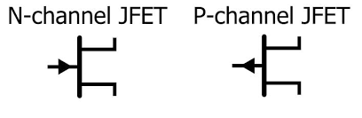
For MOSFET and JFET symbols, the gate controls the channel between drain and source. A MOSFET symbol often shows an insulated gate structure, while a JFET symbol shows a junction-controlled gate.

How Does a Transistor Symbol Work?

Main Types of Transistor Symbols

The most common transistor symbols are BJT, MOSFET, JFET, IGBT, Darlington transistor, and phototransistor symbols. Each type has a different control method and a different use case.

Transistor TypeCommon Symbol TerminalsCommon UseKey Symbol Feature
NPN BJTCollector, Base, EmitterLow-side switching, signal amplificationEmitter arrow points out
PNP BJTCollector, Base, EmitterHigh-side switching, complementary circuitsEmitter arrow points in
N-channel MOSFETDrain, Gate, SourcePower switching, motor control, LED driversGate separated from channel
P-channel MOSFETDrain, Gate, SourceHigh-side switching, reverse protectionP-channel direction marking
JFETDrain, Gate, SourceLow-noise analog circuits, input stagesGate forms a junction with channel
IGBTCollector, Gate, EmitterHigh-voltage power switchingMOS gate with bipolar output path
Darlington transistorCollector, Base, EmitterHigh-gain switchingTwo-transistor combined symbol
PhototransistorCollector, Emitter, sometimes BaseOptical sensingLight arrows point toward transistor

NPN Transistor Symbol vs PNP Transistor Symbol

The fastest way to identify NPN and PNP transistor symbols is to look at the emitter arrow. NPN points out. PNP points in.

FeatureNPN Transistor SymbolPNP Transistor Symbol
Arrow directionOutward from emitterInward toward emitter
Common switching positionLow-side switchHigh-side switch
Typical turn-on conditionBase higher than emitterBase lower than emitter
Common load pathLoad to supply, transistor to groundTransistor near supply side
Common beginner mistakeReversing collector and emitterDriving base with wrong polarity

A practical memory aid is: NPN = Not Pointing iN. The arrow points away from the base. PNP points toward the base.

NPN Transistor Symbol vs PNP Transistor Symbol

MOSFET Symbol vs BJT Symbol

A MOSFET symbol is different from a BJT symbol because a MOSFET is voltage-controlled, while a BJT is current-controlled. In a BJT, the base current controls collector-emitter current. In a MOSFET, the gate voltage controls the drain-source channel.

ItemBJT SymbolMOSFET Symbol
TerminalsCollector, Base, EmitterDrain, Gate, Source
Control methodBase currentGate-source voltage
Input behaviorRequires base currentVery high input impedance
Common PCB useSignal switching, simple driversPower switching, load control, DC-DC converters
Typical design concernBase resistor, gain variationGate drive, body diode, VGS limit
Symbol riskNPN/PNP confusionDrain/source/body diode confusion

MOSFET symbols may show enhancement or depletion mode. Depletion MOSFET symbols usually indicate a normally conductive channel, while enhancement-mode MOSFETs are normally off and are much more common in digital switching and power control.

MOSFET Symbol vs BJT Symbol

What Materials Are Used in Transistors?

Most common transistors use silicon as the semiconductor material, but advanced applications may use silicon carbide, gallium nitride, or other semiconductor materials. The symbol usually does not show the material, so the datasheet must provide that information.

MaterialCommon DevicesTypical StrengthCommon Application
SiliconBJT, MOSFET, small-signal transistorMature, cost-effective, widely availableConsumer, industrial, communication, control boards
Silicon carbideSiC MOSFET, SiC diode modulesHigh voltage, high temperature, high efficiencyEV, solar inverter, industrial power
Gallium nitrideGaN FETFast switching, high power densityChargers, RF, high-frequency power
GermaniumOlder transistor typesLow forward voltage, historical useVintage audio, legacy repair

For most PCB projects, the main issue is not the semiconductor material itself. The more urgent questions are package type, voltage rating, current rating, thermal path, availability, and assembly compatibility.

Transistor Symbol Standards and Schematic Conventions

Transistor symbols are commonly based on established diagram conventions such as IEC 60617 and IEEE/ANSI-style schematic practices. In PCB projects, the standard symbol is only one part of the library system.

Library ItemPurposeCommon Risk
Schematic symbolShows electrical functionWrong terminal naming
PCB footprintDefines copper pads and package outlineWrong pad size or pin order
3D modelChecks mechanical clearanceHeight or body mismatch
BOM dataDefines manufacturer part numberWrong substitute part
Pick-and-place dataGuides SMT placementRotation or origin error
Assembly drawingHelps inspectionMissing polarity or orientation note

A reliable symbol library saves time during engineering review. It also reduces avoidable communication problems between design teams and PCB assembly suppliers.

How to Read a Transistor Symbol on a PCB Schematic?

To read a transistor symbol correctly, start with the terminal names, then identify the transistor type, arrow direction, control pin, and connected circuit function.

StepWhat to CheckEngineering Reason
Check the reference designatorUsually Q or sometimes TConfirms it is a transistor-type component
Identify the typeBJT, MOSFET, JFET, IGBTDetermines control method
Read terminal namesC/B/E or D/G/SPrevents wrong net connection
Check arrow directionNPN, PNP, channel indicationConfirms polarity and current logic
Review nearby resistorsBase resistor, gate resistor, pull-downConfirms drive stability
Check load positionHigh-side or low-sideConfirms switching topology
Compare with datasheetPinout, ratings, packagePrevents symbol-footprint mismatch
Verify PCB footprintPad order and land patternPrevents assembly failure

A transistor symbol should never be reviewed in isolation. The symbol, component value, manufacturer part number, footprint, and circuit context must be checked together.

Transistor Symbol vs Transistor Footprint

A transistor symbol shows electrical function, while a footprint shows the physical solder pad layout on the PCB. Confusing the two is one of the most common mistakes in hardware design.

ItemTransistor SymbolTransistor Footprint
Used inSchematicPCB layout
ShowsElectrical pins and functionCopper pads, body outline, courtyard
ExampleNPN BJT symbolSOT-23, TO-92, SOT-223, DPAK
Main riskWrong circuit interpretationWrong assembly or pin connection
Checked bySchematic review, ERCDRC, footprint review, assembly drawing
Transistor Symbol vs Transistor Footprint

The transistor symbol may be electrically correct, but the PCB can still fail if the footprint is wrong. A SOT-23 transistor footprint may look simple, but pin 1, pin 2, and pin 3 must match the selected part.

How to Choose the Right Transistor Symbol for Your Circuit?

Choose the transistor symbol based on the actual transistor type, control method, circuit position, and manufacturer part number. Do not select a symbol only because it looks familiar.

Design NeedBetter Symbol ChoiceKey Check
Simple low-side load switchNPN BJT or N-channel MOSFETLoad current and drive level
High-side switchPNP BJT or P-channel MOSFETGate/base drive voltage
Fast digital switchingMOSFETGate charge and switching loss
Small-signal amplificationBJT or JFETBias point and noise level
High-voltage power controlMOSFET or IGBTVoltage rating, creepage, thermal path
Optical sensingPhototransistorLight direction and response time
High gain with simple driveDarlington transistorSaturation voltage and heat

For production boards, the symbol should include clear pin names, package link, manufacturer part number, and verified footprint mapping. Generic symbols are acceptable for early discussion, but they should be replaced or fully defined before quotation, PCB fabrication, and assembly.

Common Transistor Symbol Mistakes in PCB Design

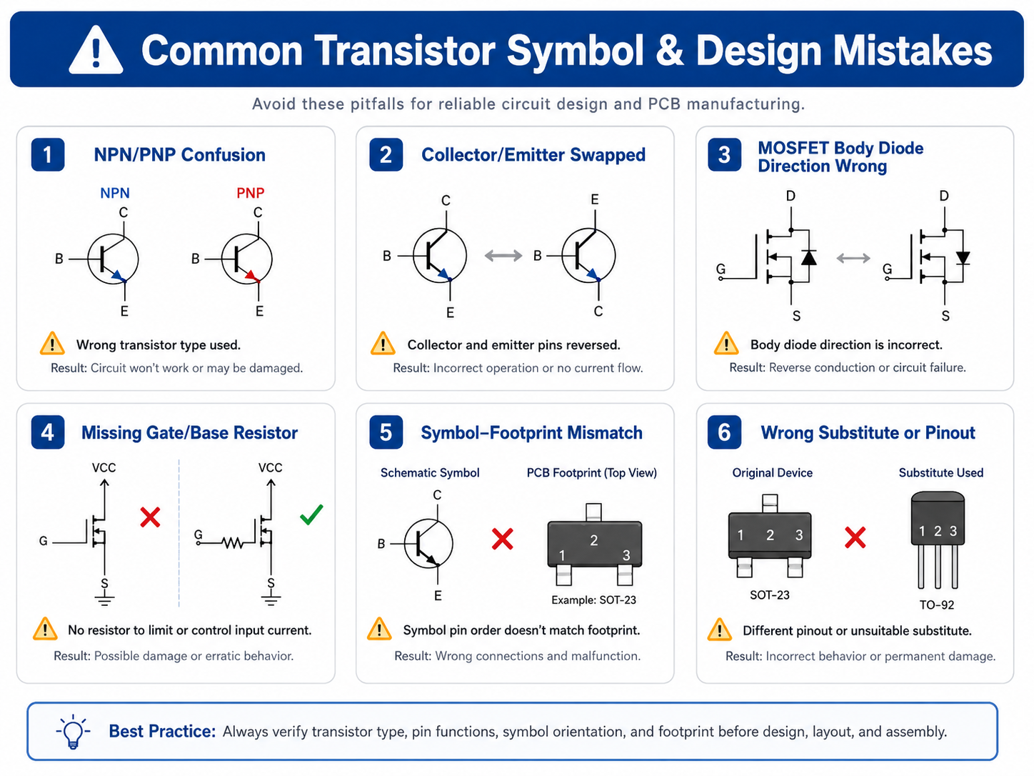
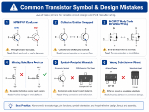
Most transistor symbol mistakes are small on the screen but expensive after assembly. They often appear during prototype bring-up, when the board does not switch, the output is inverted, or the transistor overheats.

Common Transistor Symbol Mistakes in PCB Design

A useful factory-side check is to compare the schematic symbol, footprint, BOM, and pick-and-place file before production. This review is especially valuable for small SOT-23, SOT-223, DPAK, DFN, and QFN transistor packages.

Transistor Symbol in PCB Manufacturing and PCBA Assembly

In PCB manufacturing and PCBA assembly, the transistor symbol becomes part of a larger production data chain. It starts in the schematic, moves into the PCB layout, appears in the BOM, and finally reaches SMT placement and inspection.

StageFile or DataTransistor-Related Check
Schematic designCircuit schematicCorrect symbol and pin names
PCB layoutGerber and CAD dataFootprint and copper thermal path
BOM reviewManufacturer part numberCorrect transistor type and package
SourcingApproved supplier listAvailability and substitute control
SMT programmingPick-and-place fileRotation, pin 1, centroid
Assembly inspectionAOI, visual inspectionOrientation and solder quality
Electrical testICT or functional testSwitching, gain, leakage, voltage drop

For transistor-heavy boards, quality control should not stop at solder appearance. Functional behavior must also be checked because a transistor can look correctly soldered but still be electrically wrong due to symbol, footprint, or BOM mismatch.

Testing Methods for Transistor Symbol and Circuit Accuracy

The transistor symbol itself is not tested with lab equipment, but the circuit built from that symbol can and should be verified. Testing should begin before PCB fabrication and continue through assembly and functional validation.

Test MethodWhen UsedWhat It Finds
ERC checkSchematic stageFloating base/gate, missing connections
CAD library auditBefore layout releaseSymbol-footprint mismatch
DRC checkPCB layout stageClearance, copper, pad, and routing issues
BOM reviewBefore sourcingWrong transistor type or package
Multimeter diode testDebug stageBJT junction behavior and pin identification
Oscilloscope testFunctional testSwitching waveform, ringing, delay
Thermal cameraLoad testHot transistor or weak copper area
AOI/visual inspectionAssembly stageOrientation and solder defects
X-ray inspectionHidden joints or advanced packagesVoid, bridge, or hidden solder issue

For small BJT circuits, a multimeter diode mode can help confirm base-emitter and base-collector junctions. For MOSFET circuits, check gate-source voltage, drain-source voltage, body diode direction, and gate pull-down behavior. For power circuits, thermal testing under realistic load is essential.

Quality Standards and Documentation for Transistor-Based PCB Projects

A transistor-based PCB project needs more than a correct schematic. It needs controlled documentation so the manufacturer can build the same board repeatedly.

DocumentWhy It Matters
Schematic PDFShows intended circuit function and transistor symbols
Gerber filesDefines copper, solder mask, silkscreen, and fabrication data
BOM with MPNPrevents wrong transistor sourcing
Pick-and-place fileControls SMT placement and rotation
Assembly drawingShows component orientation and special notes
Approved substitute listControls alternates without changing circuit behavior
Test planDefines switching, voltage, current, and functional checks
Quality requirementDefines IPC class, inspection criteria, and acceptance level

For overseas procurement, clear documentation reduces back-and-forth communication. It also prevents a common problem: the purchasing team buys a transistor with the same package and similar rating, but with a different pinout or switching behavior.

Industry Applications of Transistor Symbols and Transistor Circuits

Transistor symbols appear in nearly every electronic industry because transistors are core building blocks in modern circuits. The symbol helps engineers understand how control, switching, amplification, and protection are implemented.

IndustryTypical Transistor UsePCB Design Concern
Consumer electronicsSignal switching, charging, display controlCompact layout and cost control
Automotive electronicsLoad switching, sensor interface, motor controlReliability, thermal cycling, vibration
Industrial controlRelay drivers, PLC I/O, isolation circuitsSurge protection and long service life
Medical electronicsSignal conditioning, sensor circuitsStability, traceability, clean assembly
LED lightingConstant-current control, dimmingThermal management and current handling
Communication devicesRF switching, bias circuits, amplificationNoise control and impedance behavior
Power electronicsMOSFET and IGBT switchingCreepage, heat, copper thickness
Smart home devicesLow-power switching and interface circuitsStandby power and compact PCBA

In high-reliability industries, the transistor symbol is not just a drawing. It is part of design traceability. Engineers must know why a transistor was selected, how it is driven, what failure mode is expected, and whether the PCB layout supports the electrical and thermal requirement.

FAQs About Transistor Symbols

Q1: What does a transistor symbol mean?

A transistor symbol represents the electrical function of a transistor in a schematic. It shows the transistor type and terminals, such as collector, base, and emitter for BJT devices or drain, gate, and source for FET devices. The symbol helps engineers understand control direction, current path, and circuit behavior before the PCB is designed or assembled.

Q2: How can I identify an NPN transistor symbol?

An NPN transistor symbol has an arrow on the emitter pointing outward. The arrow direction shows conventional current direction at the emitter. In many low-side switching circuits, the emitter connects toward ground, the collector connects to the load, and the base receives the control signal through a resistor. Always confirm the physical pinout with the datasheet.

Q3: How can I identify a PNP transistor symbol?

A PNP transistor symbol has an arrow on the emitter pointing inward. PNP transistors are often used in high-side switching or complementary circuits. They usually turn on when the base is pulled lower than the emitter. The symbol helps identify the bias direction, but the package pinout still needs datasheet verification before PCB layout.

Q4: What is the difference between a BJT symbol and a MOSFET symbol?

A BJT symbol uses collector, base, and emitter terminals, while a MOSFET symbol uses drain, gate, and source terminals. A BJT is controlled by base current. A MOSFET is controlled by gate-source voltage. In PCB design, MOSFET symbols also require careful attention to body diode direction, gate drive voltage, and thermal dissipation.

Q5: What does the arrow mean in a transistor symbol?

The arrow usually shows conventional current direction and helps identify transistor type. In a BJT symbol, the arrow is placed on the emitter. NPN points outward, while PNP points inward. In FET symbols, arrow direction may indicate channel type or junction direction, depending on the symbol convention used in the schematic library.

Q6: Is the transistor symbol the same as the transistor footprint?

No. The transistor symbol is used in the schematic to show electrical function. The footprint is used in PCB layout to show pad shape, pad spacing, and component body position. A design can have a correct symbol but a wrong footprint. That mismatch can cause assembly failure even when the circuit idea is correct.

Q7: Why do transistor pinouts differ between similar packages?

Package appearance does not guarantee the same pin order. Two SOT-23 or TO-92 transistors may have different internal pin arrangements depending on manufacturer and part number. This is why engineers must verify the datasheet, symbol-to-footprint mapping, and BOM before releasing PCB files for fabrication and assembly.

Q8: What is the common reference designator for a transistor?

The common reference designator for a transistor is usually Q, such as Q1, Q2, or Q15. Some older drawings may use other letters, but Q is widely recognized in PCB schematics. A clear reference designator helps connect schematic symbols, BOM lines, PCB footprints, assembly drawings, and inspection records.

Q9: Can I use a generic transistor symbol in my schematic?

A generic symbol can be used during early concept design, but production schematics should define the exact transistor type, pin names, package, and manufacturer part number. Generic symbols increase the risk of wrong pin mapping, wrong package selection, and sourcing mistakes. For PCBA production, a controlled library is much safer.

Q10: What causes a transistor circuit to fail after PCB assembly?

Common causes include wrong NPN/PNP selection, incorrect MOSFET drain-source direction, symbol-footprint mismatch, missing gate or base resistor, floating gate, wrong substitute part, insufficient copper for heat dissipation, or incorrect assembly orientation. A complete review should compare the schematic, datasheet, BOM, footprint, pick-and-place file, and functional test result.

Conclusion

A transistor symbol is small, but it carries critical design information. It identifies the transistor type, terminal function, current direction, control method, and circuit behavior. For reliable PCB and PCBA production, the symbol must match the datasheet, footprint, BOM, assembly orientation, and test plan.

If you are sourcing reliable PCB/PCBA manufacturing, including OEM, ODM, prototyping, mass production, or custom engineering solutions, reach out to our engineering team for technical support and a quote at sales@bestpcbs.com.

You may also like

Transistor Symbol Meaning, Function, Types & How to Read it?
Thursday, April 23rd, 2026

In modern electronics, the transistor symbol is one of the most frequently used elements in circuit schematics. It appears in almost every design, from simple switching circuits to complex multi-layer PCB systems. While the physical transistor is a semiconductor device, the symbol is what engineers rely on to interpret how that device behaves inside a circuit.

For engineers, designers, and even procurement teams reviewing schematics, understanding transistor symbols is essential. It helps you quickly identify signal paths, determine control logic, and verify whether a circuit is designed correctly. Without this knowledge, even a well-documented schematic can become difficult to interpret.

Transistor Symbol Meaning, Function, Types & How to Read it?

Transistor Symbol Meaning, Function, Types & How to Read it?

What Is a Transistor Symbol in Electronics?

A transistor symbol is a simplified graphical representation used in circuit diagrams to show how a transistor connects and behaves within an electronic system. It does not show the physical shape of the device. Instead, it highlights electrical terminals and signal flow direction so engineers can quickly understand circuit behavior.

In practical design work, the transistor symbol becomes a universal language. Whether you are reviewing a schematic or debugging a PCB, this symbol helps you identify amplification stages, switching paths, and control nodes without ambiguity.

At its core, the symbol communicates three essential things:

  • The number of terminals (typically three)
  • The direction of current flow
  • The type of transistor (NPN or PNP)
What Is a Transistor Symbol in Electronics?

Because modern electronics rely heavily on transistor-based circuits, understanding this symbol is not optional. It is a foundational skill for anyone working in PCB design, embedded systems, or hardware development.

Is a Transistor Current or Voltage?

A transistor is both a current-controlled device and a voltage-controlled device, depending on the type and how it is used in a circuit. This dual nature is what makes it extremely versatile in electronics.

For BJT (Bipolar Junction Transistor) devices:

  • The transistor is mainly current-controlled
  • A small base current controls a larger collector current
  • This behavior is ideal for amplification

For FET (Field Effect Transistor) devices:

  • The transistor is mainly voltage-controlled
  • The gate voltage controls current flow between drain and source
  • This makes it efficient for switching applications

In real-world PCB applications, engineers often choose between these behaviors depending on the design goal. If precise current amplification is needed, BJT is preferred. If low power control is required, FET becomes the better choice.

Transistor Symbol Function in Circuit Design

The transistor symbol plays a critical role in circuit design because it defines how signals move and interact. It is not just a drawing. It is a compact representation of functionality.

In circuit schematics, the symbol helps engineers:

  • Identify switching points in digital circuits
  • Understand amplification paths in analog designs
  • Trace signal direction quickly during debugging
  • Design logic gates and control systems

For example, in a switching circuit, the transistor symbol clearly shows whether current will flow when a signal is applied. In an amplifier, it helps determine gain direction and biasing requirements.

Transistor Symbol Function in Circuit Design

Without a clear symbol, interpreting a circuit would be slow and error-prone. That is why every PCB layout begins with a well-structured schematic using standard transistor symbols.

What Does a Transistor Symbol Represent in a Circuit?

A transistor symbol represents the internal structure and electrical behavior of the device. Even though the internal semiconductor layers are not shown, the symbol gives enough information to understand how it works.

The three terminals shown in a typical BJT symbol are:

  • Emitter (E) – where current exits
  • Base (B) – control terminal
  • Collector (C) – where current enters

The arrow on the emitter is the most important visual element. It indicates current direction and identifies the transistor type.

What the symbol conveys:

  • Direction of conventional current
  • Control relationship between terminals
  • Type of charge carriers (indirectly)
  • Switching or amplification role in the circuit

In short, the transistor symbol acts as a bridge between physical semiconductor behavior and practical circuit design.

How to Read a Transistor Symbol Step by Step?

Reading a transistor symbol becomes simple when you follow a structured approach. This avoids confusion, especially when working with complex schematics.

Step-by-step method:

  1. Identify the three terminals
    • Look for base, collector, and emitter
    • The base is usually the middle line
  2. Locate the arrow
    • The arrow is always on the emitter
    • It shows current direction
  3. Determine transistor type
    • Arrow pointing out → NPN
    • Arrow pointing in → PNP
  4. Check connections
    • See how each terminal connects to other components
    • This reveals the transistor’s role
  5. Understand function in context
    • Is it switching?
    • Is it amplifying?
    • Is it part of a logic circuit?

This method works reliably across most circuit diagrams, from simple educational circuits to high-density industrial PCBs.

Does a Transistor Follow Ohm’s Law?

A transistor does not strictly follow Ohm’s law because it is not a simple resistive device. Ohm’s law applies to linear components like resistors, where voltage and current have a direct relationship.

However, parts of a transistor circuit may still obey Ohm’s law. For example:

  • The resistors connected to the transistor follow Ohm’s law
  • Biasing networks are often calculated using Ohm’s law
  • Load resistors determine current levels

Inside the transistor itself, behavior is nonlinear. The relationship between voltage and current depends on semiconductor physics rather than a fixed resistance.

So in practice:

  • Use Ohm’s law for surrounding components
  • Use transistor equations or datasheets for device behavior

What are the Two Types of Transistors?

The two primary types of transistors used in electronics are:

  • BJT (Bipolar Junction Transistor)
  • FET (Field Effect Transistor)

Within BJT, there are two subtypes:

  • NPN transistor
  • PNP transistor
What are the Two Types of Transistors?

Within FET, common types include:

  • MOSFET
  • JFET

Each type serves different roles in circuit design.

Key differences:

  • BJT uses current control
  • FET uses voltage control
  • FET typically offers higher input impedance
  • BJT often provides stronger gain in analog circuits

In PCB assembly projects, the choice depends on performance targets such as speed, power consumption, and signal integrity.

How to Tell if a Transistor is NPN or PNP?

The easiest way to identify a transistor type is by looking at the arrow in the symbol.

  • NPN transistor
    • Arrow points outward
    • Current flows out of the emitter
  • PNP transistor
    • Arrow points inward
    • Current flows into the emitter

Another way is by analyzing circuit connections:

  • NPN typically connects emitter to ground
  • PNP often connects emitter to positive voltage

In real PCB troubleshooting, this visual identification saves time and prevents wiring mistakes.

NPN vs PNP Transistor Symbols: What Are the Key Differences?

Understanding the difference between NPN and PNP transistor symbols is essential for accurate circuit interpretation.

FeatureNPN TransistorPNP Transistor
Arrow DirectionOutwardInward
Current FlowEmitter to groundFrom supply to emitter
Control SignalPositive base voltageNegative base voltage
Common UseSwitching, amplificationHigh-side switching
PopularityMore widely usedLess common

This comparison highlights why NPN transistors are more frequently used in modern designs. They are easier to integrate with standard logic levels.

Which Transistor is Faster, NPN or PNP?

In most cases, NPN transistors are faster than PNP transistors.

This is due to the mobility of charge carriers:

  • NPN uses electrons, which move faster
  • PNP uses holes, which move slower

Because of this:

  • NPN transistors switch faster
  • They are preferred in high-speed circuits
  • They are widely used in digital electronics

For applications like signal processing or fast switching, NPN devices are often the first choice.

What is a Transistor Used For?

Transistors are the backbone of modern electronics. They serve multiple roles across different types of circuits.

Common applications include:

  • Signal amplification
  • Electronic switching
  • Voltage regulation
  • Logic gate construction
  • Power control

In PCB manufacturing, transistors are used in:

  • Power supply circuits
  • Communication modules
  • Automotive electronics
  • Industrial control systems

Their ability to control large currents with small signals makes them indispensable in both simple and complex designs.

How to Tell If a Transistor is Bad?

A faulty transistor can cause circuit failure or unstable performance. Identifying a bad transistor is a key diagnostic skill.

Common signs include:

  • No switching action
  • Overheating
  • Unexpected voltage readings
  • Signal distortion

Basic testing steps:

  1. Use a multimeter in diode mode
  2. Check base-emitter junction
  3. Check base-collector junction
  4. Compare readings with expected values

If the readings are inconsistent or show short circuits, the transistor may be damaged.

In production environments, more advanced testing methods like curve tracing or functional testing are used to ensure reliability.

FAQs

1. What is the meaning of a transistor symbol?
A transistor symbol shows how the device connects and how current flows. It simplifies complex semiconductor behavior into a clear diagram.

2. Why is the arrow important in a transistor symbol?
The arrow indicates current direction and helps identify whether the transistor is NPN or PNP.

3. Can a transistor work without a symbol in a diagram?
In practice, no. Without the symbol, it becomes difficult to interpret circuit function and connections.

4. Is the transistor symbol the same worldwide?
Yes, standard symbols are used globally to ensure consistency across designs and documentation.

5. Do all transistors have three terminals?
Most common transistors have three terminals, but some specialized devices may differ.

Conclusion

From identifying NPN and PNP types to understanding signal flow and functionality, mastering this symbol unlocks deeper insight into electronic systems. It also reduces design errors and speeds up development cycles.

If you are working on PCB design, assembly, or electronic product development, having a clear understanding of transistor symbols will directly improve your efficiency and accuracy.

For professional PCB fabrication and PCBA support, feel free to reach out to our engineering team at sales@bestpcbs.com.

You may also like