PCB manufacturing PCB manufacturing
Home > Blog

RF & Telecom PCB Manufacturer

June 15th, 2026

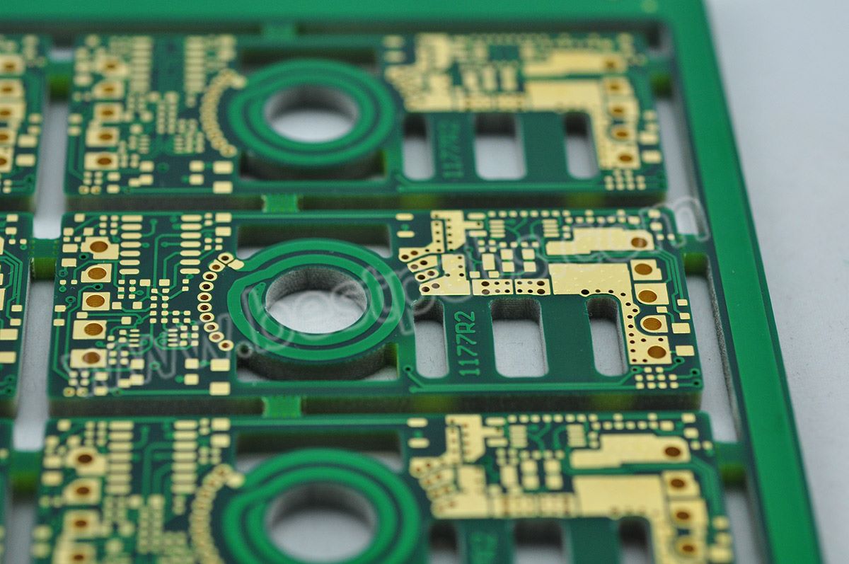
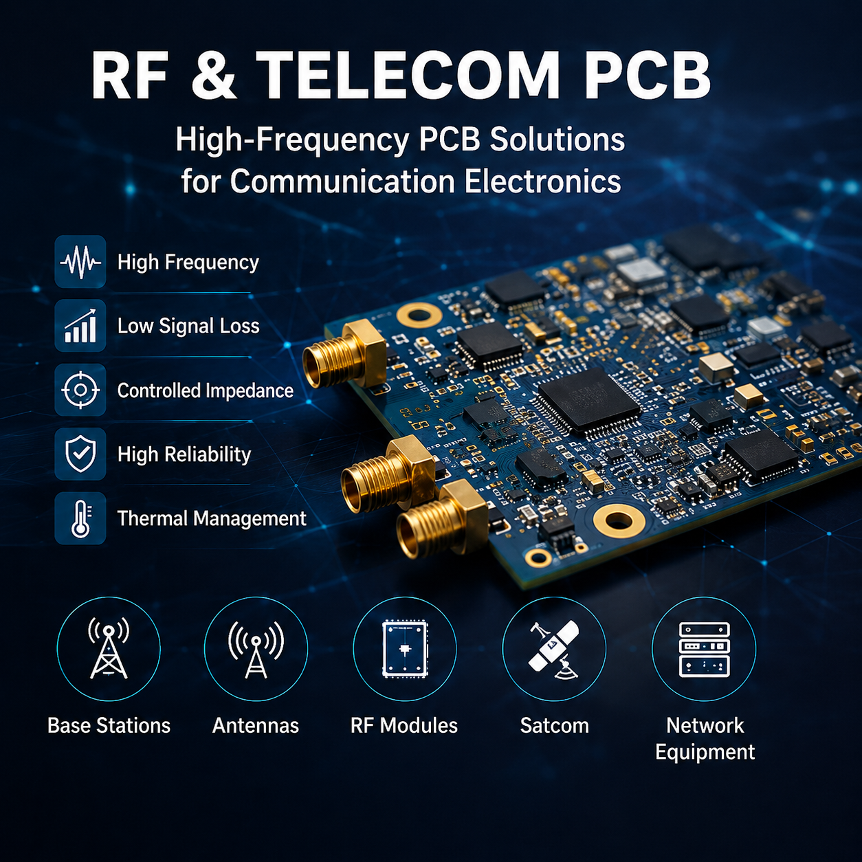
RF & Telecom electronics depend on stable signal transmission. At high frequencies, small changes in material, dielectric thickness, copper roughness, impedance, stack-up, or surface finish can affect circuit performance. Because of this, RF & Telecom PCB manufacturing requires more than standard PCB fabrication. It needs suitable materials, controlled impedance, precise stack-up management, reliable testing, and engineering review before production.
RF & Telecom PCB Manufacturer

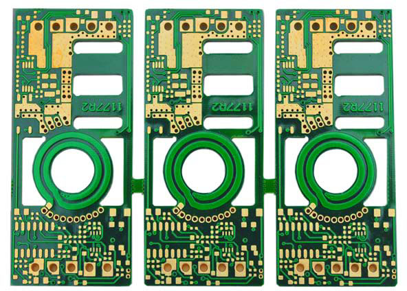
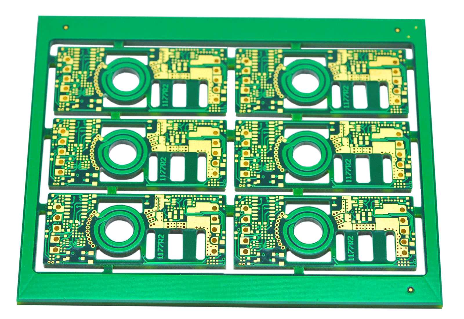
EBest Circuit supports RF and telecom PCB projects that require high-frequency materials, controlled impedance, multilayer stack-up control, thermal management, PCB assembly, and project documentation. Our capabilities include RF PCB, high-frequency PCB, HDI PCB, rigid-flex PCB, heavy copper PCB, metal core PCB, ceramic PCB, multilayer PCB, and PCBA services.

From RF PCB prototypes to telecom batch production, our engineering and manufacturing teams help customers review design feasibility, reduce manufacturing risks, and build reliable circuit boards for communication electronics.

Why RF & Telecom PCB Projects Need More Than Standard PCB Manufacturing?

RF & Telecom PCB refers to printed circuit boards used in radio frequency and communication electronics. These boards are commonly found in wireless communication products, antenna systems, RF front-end modules, radar electronics, satellite communication equipment, network devices, optical communication systems, and telecom infrastructure.

Unlike standard PCBs, RF and telecom PCBs must support stable signal transmission. At higher frequencies, a PCB trace is not just a copper connection. It acts as a transmission line. Its width, spacing, copper thickness, dielectric thickness, material properties, reference plane, and surface finish can all influence signal behavior.

This is why RF & Telecom PCB projects need a manufacturer with high-frequency PCB experience, not only a supplier that can build basic boards.

Customers usually need more than open and short testing. They may need controlled impedance, low signal loss, stable stack-up, consistent materials, impedance test reports, PCBA support, and clear production documentation.

At EBest Circuit, RF and telecom PCB manufacturing is handled as an engineering-driven process. We review material selection, stack-up, impedance targets, copper thickness, via structures, thermal paths, and assembly requirements before production when needed.

What Makes RF & Telecom PCBs Difficult to Build?

RF and telecom PCBs are difficult to build because small production variables can affect performance. A board may pass basic electrical testing but still perform poorly in an RF circuit if impedance, material loss, or signal transition is not controlled.

  • High-frequency signals are sensitive to dielectric constant and dissipation factor. If the material is not suitable for the operating frequency, signal loss may increase.
  • Controlled impedance is also critical. RF circuits often use 50-ohm single-ended impedance, while high-speed telecom circuits may require 90-ohm or 100-ohm differential impedance. Impedance can shift if trace width, spacing, dielectric thickness, or copper thickness is not controlled.
  • Stack-up design affects return paths, shielding, crosstalk, and signal stability. RF layers need proper reference planes and stable dielectric spacing. Poor stack-up planning may cause signal reflection, EMI issues, or inconsistent performance.
  • Via design is another key factor. Via transitions, via stubs, ground vias, and layer changes can affect RF and high-speed signals. The design must balance electrical performance and manufacturability.
  • Surface finish and copper profile may also influence high-frequency behavior. At higher frequencies, signal current tends to flow near the conductor surface, so copper roughness and surface treatment can affect loss.

Telecom equipment often needs stable performance over long operating periods. For base stations, antenna modules, RF front-end circuits, network devices, and optical communication equipment, repeatable manufacturing is as important as the first successful prototype.

Our RF & Telecom PCB Manufacturing Capabilities

EBest Circuit supports RF and telecom PCB projects across different board structures, materials, and production stages. We help customers choose suitable manufacturing solutions according to frequency, impedance target, thermal load, board size, assembly method, and production volume.

Our RF and telecom PCB capabilities include:

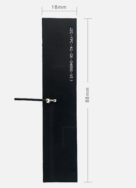
  • RF PCB for antenna modules, RF front-end circuits, wireless communication products, and microwave systems
  • High-frequency PCB using RF laminates and customer-specified high-frequency materials
  • Controlled impedance PCB for RF and high-speed telecom signals
  • Multilayer telecom PCB for communication equipment, network systems, and control modules
  • HDI PCB for compact communication products and high-density routing
  • Rigid-flex PCB for space-limited RF and telecom assemblies
  • Hybrid stack-up PCB combining RF materials with FR4 or other substrates
  • Heavy copper PCB for telecom power control and current-carrying circuits
  • Metal core PCB for RF power modules and thermal management applications
  • Ceramic PCB for high-power, high-heat, and dimensionally stable electronic modules
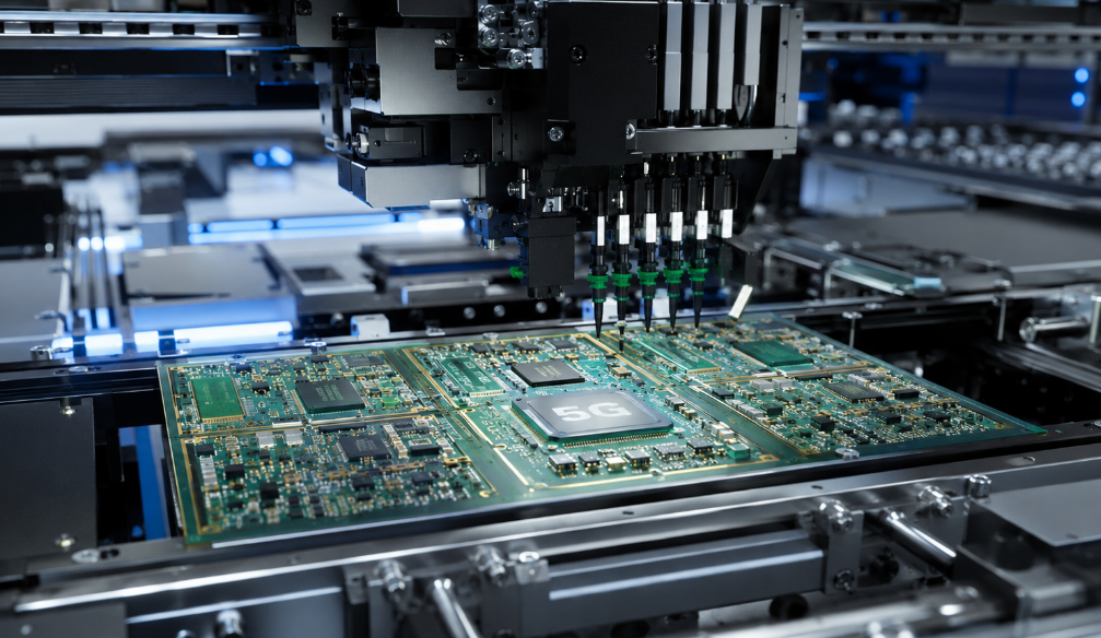
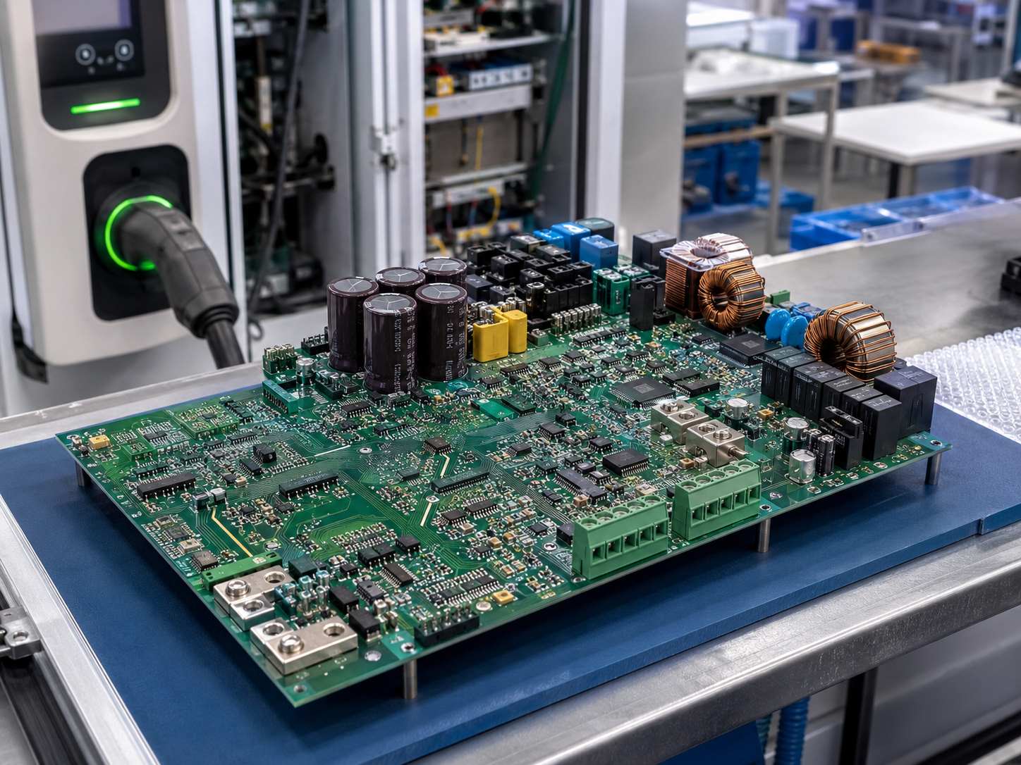
  • PCBA service for PCB fabrication, component sourcing, SMT assembly, inspection, testing, and box-build support

Different communication products require different PCB structures. An antenna module may require low-loss RF laminate and controlled impedance. A telecom control board may need multilayer FR4 with impedance control. A compact communication device may require HDI or rigid-flex PCB. A power amplifier module may need heavy copper, metal core, or ceramic PCB for heat dissipation.

Our engineering team can review the design and suggest a practical manufacturing route before production.

What Types of PCBs Are Used in RF and Telecom Equipment?

RF and telecom equipment can use different PCB types depending on frequency, signal speed, power level, mechanical layout, heat dissipation, and cost target.

RF PCB is used for radio frequency circuits, including antenna modules, RF front-end boards, wireless communication products, microwave systems, and signal transmission modules. RF PCB manufacturing requires careful control of material properties, impedance, dielectric spacing, copper thickness, and surface quality.

High-frequency PCB is used when the circuit works at higher frequencies and needs lower signal loss. These boards often use RF laminates, PTFE-based materials, ceramic-filled materials, or other high-frequency substrates. They are common in radar, microwave communication, satellite communication, and advanced wireless systems.

Telecom equipment often uses multilayer PCBs because the design may include RF signals, high-speed digital signals, power distribution, grounding, shielding, and control circuits. A stable multilayer stack-up helps improve routing density, signal integrity, and EMC performance.

Controlled impedance PCB is widely used in RF and telecom electronics. The board must be manufactured according to defined impedance targets. This requires coordination between design, material selection, stack-up, trace geometry, copper thickness, and manufacturing tolerance.

HDI PCB is suitable for compact telecom products, RF modules, IoT communication devices, and high-density control systems. Microvias, blind vias, buried vias, and fine lines help reduce board size while supporting complex routing.

Rigid-flex PCB can reduce connectors, save space, and improve mechanical reliability. It is suitable for compact communication equipment, antenna systems, portable RF modules, and assemblies where cable reduction is important.

Heavy copper PCB is used for power supply sections, current-carrying circuits, and telecom power modules. It improves current capacity and supports better heat spreading in power areas.

Metal core PCB helps transfer heat away from power components. Aluminum base and copper base PCBs can be used in RF power modules, LED communication modules, and telecom thermal management designs.

Ceramic PCB offers high thermal conductivity, dimensional stability, and electrical insulation. It can be used in high-power RF modules, microwave circuits, laser communication modules, and high-heat telecom applications.

Materials We Support for RF & Telecom PCB Applications

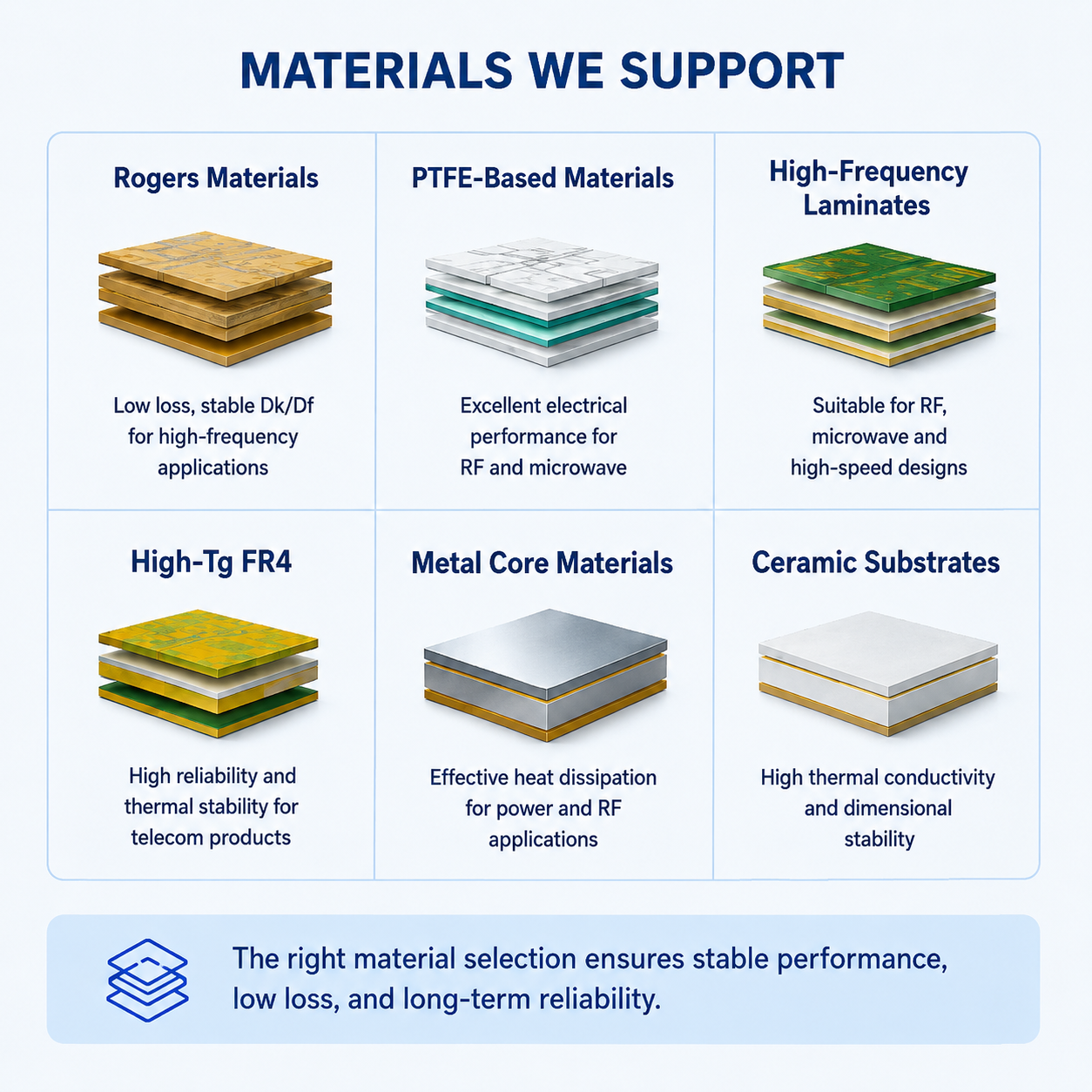
Material selection is one of the most important decisions in RF and telecom PCB manufacturing. The material affects impedance, signal speed, insertion loss, thermal behavior, dimensional stability, and cost.

EBest Circuit can support RF and telecom PCB projects using different material options based on customer requirements.
RF & Telecom PCB

High-frequency laminates are used when low loss and stable electrical performance are required. They are suitable for RF circuits, microwave circuits, antenna boards, satellite communication modules, and radar-related applications.

Rogers materials are commonly used in RF and microwave PCB applications because they offer more stable electrical properties and lower loss than standard FR4 in many high-frequency designs. They are often selected for antenna systems, RF modules, radar boards, and telecom equipment.

PTFE-based materials are widely used in RF and microwave circuits. They support low-loss signal transmission and stable dielectric behavior, making them suitable for high-frequency applications.

Not every telecom PCB requires RF laminate across the whole board. Some communication products use high-speed FR4 or high-Tg FR4 for digital, control, or power sections, while RF areas use special high-frequency materials.

Hybrid stack-up is useful when a design combines RF circuits with standard digital or power circuits. It can help balance performance and cost. However, hybrid material construction needs careful lamination control because different materials may have different thermal expansion and bonding behavior.

Aluminum and copper base materials can be used when RF or telecom modules generate heat. Metal core PCB helps improve heat transfer from power devices and supports stable operation in thermal-sensitive designs.

Ceramic substrates are suitable for compact, high-power, and high-heat RF or telecom modules. They provide good thermal conductivity, electrical insulation, and dimensional stability.

Material selection should be based on operating frequency, impedance target, insertion loss requirement, board thickness, thermal load, cost target, and production volume.

Controlled Impedance and Stack-Up Engineering Support

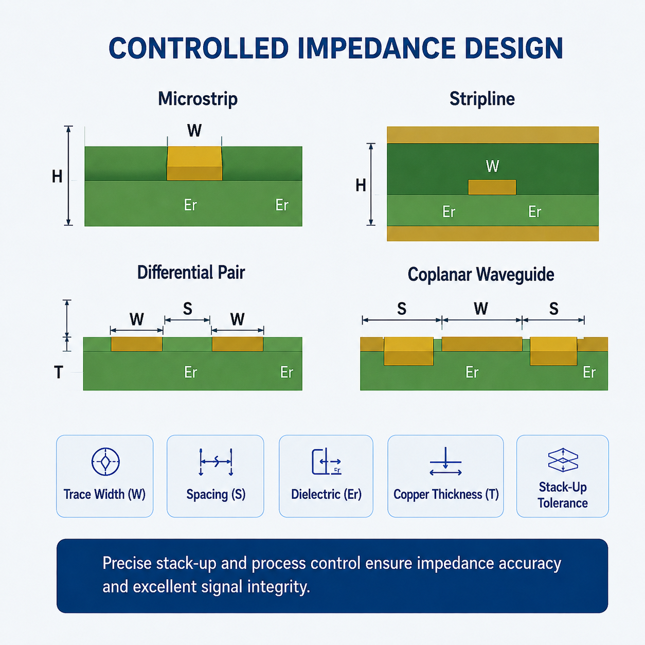
Controlled impedance is central to RF & Telecom PCB manufacturing. Many RF circuits use 50-ohm impedance. High-speed telecom circuits may require 90-ohm or 100-ohm differential impedance. Other values may also be used depending on the design.

Impedance is affected by:

  • Trace width
  • Trace spacing
  • Copper thickness
  • Dielectric thickness
  • Dielectric constant
  • Solder mask thickness
  • Reference plane distance
  • Stack-up structure
  • Manufacturing tolerance

If these factors are not controlled, the board may have impedance deviation. This can cause signal reflection, signal loss, timing issues, EMI problems, or unstable RF performance.
RF & Telecom PCB Manufacturer

Our engineering team can review your stack-up before production. This review may include dielectric thickness, copper thickness, layer arrangement, impedance targets, trace width, spacing, reference planes, solder mask influence, and impedance coupon design.

We can support different transmission line structures, including:

  • Microstrip
  • Stripline
  • Coplanar waveguide
  • Differential pairs
  • RF transmission lines
  • Controlled impedance signal layers

For projects that require impedance testing, we can review the test requirements and arrange impedance coupons according to the design. This helps customers confirm whether the manufactured board meets the required impedance range.

Signal Integrity, Loss Control, and RF Design Factors

RF and telecom PCB performance depends on the full signal path, including traces, vias, pads, connectors, reference planes, grounding, shielding, and layer transitions.

Insertion loss refers to signal loss through the transmission path. It can be affected by material dissipation factor, copper roughness, trace length, frequency, surface finish, and via transitions. Lower loss is important for many RF and telecom applications.

Return loss is related to signal reflection. If impedance is not well controlled, part of the signal may reflect back instead of continuing through the line. This can affect RF performance and communication quality.

Dense telecom boards may include many high-speed signals. Poor spacing, weak reference planes, or improper routing can increase crosstalk. Proper layer planning and routing rules help reduce interference.

Vias can create discontinuities in RF and high-speed paths. Via stub length, anti-pad design, ground via placement, and layer transition structure may affect signal performance.

RF circuits need stable grounding and proper shielding. Ground vias, via fences, reference planes, and shield cans may be used to reduce unwanted coupling and radiation.

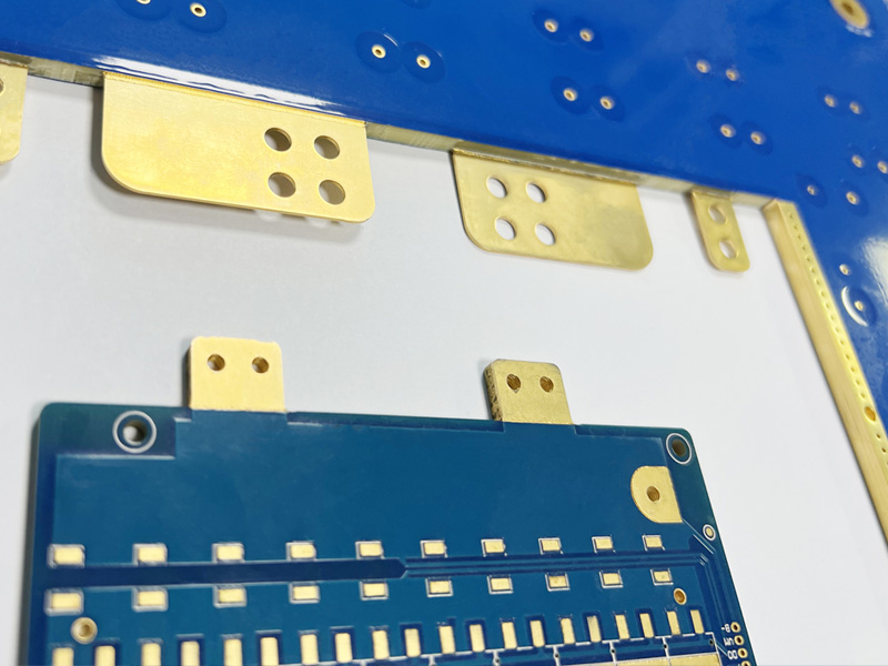
Surface finish affects solderability, flatness, contact performance, and high-frequency behavior. The suitable finish should be selected according to RF performance, assembly requirements, storage needs, and customer specifications.

Many telecom products contain both RF circuits and high-speed digital circuits. These areas may have different design rules. A proper stack-up and grounding strategy can help reduce interference between functional sections.

Our team helps review manufacturability risks and production variables that may affect performance, including material selection, stack-up, copper thickness, impedance control, via structure, surface finish, and assembly feasibility.

Thermal Management for RF and Telecom Power Modules

RF and telecom PCB projects are not only about signal performance. Many communication products also generate heat. RF power amplifiers, base station modules, telecom power boards, LED communication devices, and power conversion circuits may require better thermal management.

Heat can affect component life, signal stability, solder joint reliability, and long-term product performance. If thermal paths are not designed properly, heat may concentrate around power devices.

Thermal management may involve:

  • Heavy copper for higher current and heat spreading
  • Thermal vias for heat transfer between layers
  • Copper balancing for manufacturing stability
  • Metal core PCB for heat dissipation
  • Copper base PCB for stronger thermal transfer
  • Aluminum base PCB for cost-effective heat dissipation
  • Ceramic PCB for thermal conductivity and electrical insulation
  • Component placement for shorter thermal paths
  • Heat sink connection areas
  • Thermal pad and solder mask opening control

EBest Circuit supports heavy copper PCB, metal core PCB, copper base PCB, aluminum PCB, and ceramic PCB for RF and telecom modules that require better heat dissipation.

For power-related telecom projects, our engineering team can review copper thickness, thermal vias, base material, heat transfer path, solder mask design, and assembly requirements before production.

Quality Control for RF & Telecom PCB Manufacturing

For RF and telecom PCB projects, quality control is not only open and short testing. It also includes stable materials, accurate stack-up, controlled impedance, plating consistency, and repeatable production.

Our quality control process can include:

  • Incoming material inspection
  • Engineering file review
  • Stack-up confirmation
  • Inner layer AOI
  • Lamination process control
  • Drilling inspection
  • Plating thickness control
  • Solder mask inspection
  • Surface finish inspection
  • Electrical testing
  • Impedance testing when required
  • Microsection analysis when required
  • Final visual inspection
  • Packing inspection
  • Traceability documentation

For controlled impedance projects, test coupons can be used to verify impedance performance. For multilayer telecom PCBs, stable lamination and dielectric thickness control are important. For RF PCBs, material handling, surface quality, and process consistency need careful control.

For PCBA projects, additional inspection can include:

  • BOM review
  • Component sourcing control
  • Solder paste inspection
  • SMT placement inspection
  • Reflow process control
  • AOI inspection
  • X-ray inspection for BGA or hidden solder joints
  • RF connector assembly inspection
  • Functional testing when required
  • Conformal coating when required
  • Final assembly inspection

Quality for RF & Telecom PCB manufacturing depends on correct material selection, practical stack-up, stable fabrication, controlled assembly, and clear inspection requirements.

PCB Assembly Support for RF & Telecom Electronics

Many customers need more than bare PCB fabrication. RF and telecom projects may require PCB assembly, component sourcing, RF connector assembly, shield can assembly, functional testing, and box-build service.

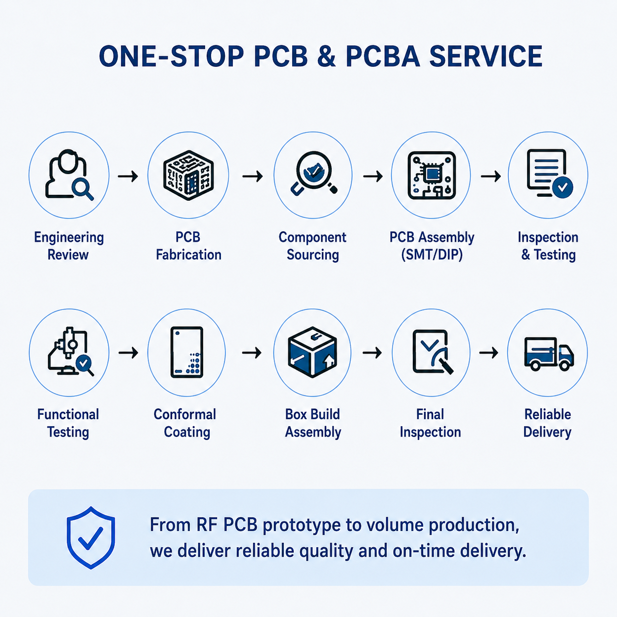
EBest Circuit provides PCB and PCBA one-stop support to help customers reduce supplier coordination work. Customers can combine PCB fabrication, component sourcing, SMT assembly, inspection, testing, and final packaging with one team.
RF & Telecom PCB Manufacturer

Our PCBA capabilities include:

  • SMT assembly
  • DIP assembly
  • Fine-pitch component assembly
  • BGA assembly
  • QFN and QFP assembly
  • RF connector assembly
  • Shield can assembly
  • Component sourcing support
  • BOM review
  • PCB fabrication and assembly coordination
  • SPI inspection
  • AOI inspection
  • X-ray inspection
  • Functional testing
  • Conformal coating
  • Box-build assembly

Assembly quality can affect RF and telecom product performance. Connector alignment, solder joint quality, shielding structure, cleaning, reflow profile, and component placement all need attention.

For projects that require testing, our team can review the customer’s functional test method before production. If special RF testing is required, we can discuss the test conditions and support production coordination based on customer specifications.

From RF PCB Prototype to Telecom Batch Production

RF and telecom projects often start with prototypes. Engineers may need to verify frequency performance, impedance, material choice, antenna behavior, thermal design, connector structure, and assembly feasibility before moving to batch production.

EBest Circuit supports customers through different project stages:

  • RF PCB prototype
  • Engineering sample
  • Design verification build
  • Small-batch production
  • Pilot run
  • Telecom batch production
  • Repeat order manufacturing
  • PCB assembly and testing
  • Box-build support when required

For prototype projects, customers often need fast feedback and practical manufacturability suggestions. Our engineering team can review the design and point out issues related to material, stack-up, drill design, impedance, copper thickness, or assembly.

For batch production, customers need stable material supply, repeatable processes, controlled inspection, and clear documentation.

Because we support both prototype and production stages, customers can move from early design review to later production with better continuity.

What Files Should You Send for an RF & Telecom PCB Quote?

A complete quotation package helps our engineering team evaluate your RF & Telecom PCB project faster and more accurately. Because RF and telecom designs are sensitive to materials and stack-up, complete information helps improve quotation accuracy.

For bare PCB fabrication, please prepare:

  • Gerber files
  • Drill files
  • Stack-up requirement
  • Material brand or material type
  • Target frequency if available
  • Impedance requirement
  • Copper thickness
  • Board thickness
  • Surface finish
  • Solder mask requirement
  • Silkscreen requirement
  • Controlled impedance tolerance
  • Impedance test requirement
  • Special via structure requirement
  • Quantity
  • Expected lead time
  • Testing requirement
  • Special documentation requirement

For PCBA projects, please also provide:

  • BOM
  • CPL or pick-and-place file
  • Assembly drawing
  • RF connector requirement
  • Shielding requirement
  • Functional test instruction if available
  • Programming requirement if needed
  • Conformal coating requirement if needed
  • Box-build documents if required

If your files are not complete, you can send the available files first. Our engineering team can help check what information is missing before quotation.

Why Choose EBest Circuit for RF & Telecom PCB Projects?

Choosing an RF & Telecom PCB manufacturer is about more than price. A supplier should be able to support material review, impedance control, stack-up engineering, thermal management, reliable manufacturing, PCBA, and technical communication.

EBest Circuit supports RF and telecom PCB projects through manufacturing experience, wide PCB capability, engineering support, quality control, and one-stop PCB assembly service.

Founded in 2006, EBest Circuit has long-term experience in PCB manufacturing and PCB assembly. We serve customers in communication electronics, industrial control, automotive electronics, medical devices, power electronics, aerospace-related electronics, and other high-reliability fields.

This experience helps us understand the requirements of RF and telecom projects, including materials, impedance, signal behavior, thermal performance, assembly quality, and production consistency.

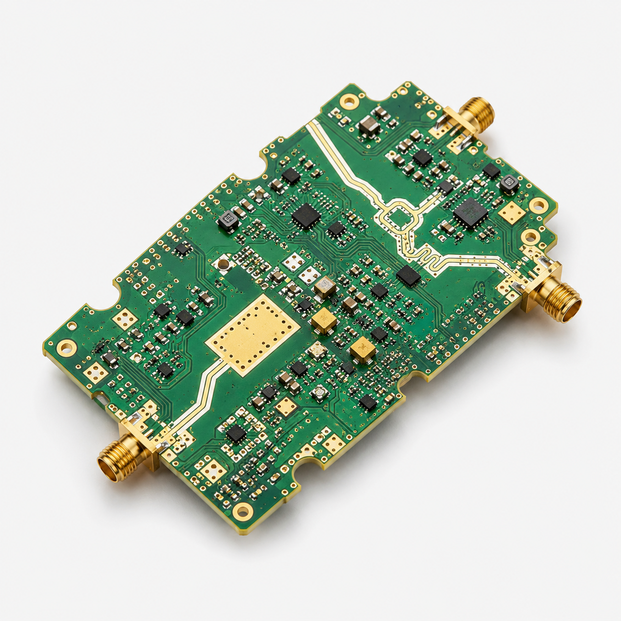
Our capabilities include RF PCB, high-frequency PCB, controlled impedance PCB, multilayer PCB, HDI PCB, rigid-flex PCB, heavy copper PCB, metal core PCB, ceramic PCB, and PCBA.
RF & Telecom PCB Manufacturer

This gives customers more flexibility when choosing the right board structure for communication equipment, RF modules, antenna systems, power boards, and high-speed telecom products.

We do not only quote from Gerber files. Our engineering team can review material selection, stack-up, impedance targets, copper thickness, via structure, RF routing risks, thermal paths, and assembly feasibility before production.

We can support RF and telecom PCB projects using customer-specified high-frequency materials and controlled impedance requirements. Our team can review dielectric thickness, trace width, spacing, copper thickness, reference planes, and impedance coupons according to project needs.

We provide PCB fabrication, component sourcing support, SMT assembly, DIP assembly, inspection, functional testing, conformal coating, and box-build support. This helps customers reduce supplier management work and improve project communication.

We support RF PCB prototypes, engineering samples, small batches, pilot runs, batch production, and repeat orders. Customers can work with one manufacturing partner from early development to later production.

Our quality management approach supports controlled manufacturing, inspection, testing, and documentation. For projects with special quality, traceability, or inspection requirements, our team can review the details before production.

RF and telecom projects often involve technical questions. Our team can communicate with customers about material options, stack-up feasibility, impedance control, testing needs, assembly risks, and delivery planning.

Frequently Asked Questions About RF & Telecom PCB Manufacturing

  • What is an RF & Telecom PCB?

An RF & Telecom PCB is a printed circuit board used in radio frequency and communication electronics. Common applications include antenna modules, RF front-end circuits, wireless devices, base station equipment, radar modules, satellite communication systems, optical communication devices, and network equipment.

  • What is the difference between RF PCB and standard PCB?

A standard PCB mainly provides electrical connections. An RF PCB must also control signal loss, impedance, dielectric behavior, copper quality, grounding, shielding, and signal path stability. It usually requires more careful material selection and stack-up control.

  • What materials are used for RF PCB manufacturing?

RF PCB materials may include Rogers materials, PTFE-based materials, high-frequency laminates, ceramic-filled substrates, high-speed FR4, high-Tg FR4, metal core materials, and ceramic substrates. The best material depends on frequency, loss target, impedance requirement, thermal needs, cost, and production volume.

  • Can you manufacture Rogers PCB?

Yes. We can support RF and high-frequency PCB projects using Rogers materials and other customer-specified RF laminates. Please send your material requirement, stack-up, Gerber files, and impedance targets for engineering review.

  • Can RF PCB combine Rogers and FR4 materials?

Yes. Some RF and telecom designs use hybrid stack-up structures that combine RF materials with FR4 or other materials. This can help balance performance and cost, but it requires careful lamination and stack-up review before production.

  • Why is controlled impedance important for telecom PCB?

Controlled impedance helps maintain signal stability and reduce signal reflection, timing issues, and transmission problems. In telecom PCB designs, impedance is affected by trace width, spacing, dielectric thickness, copper thickness, material properties, and reference plane design.

  • What surface finish is suitable for RF PCB?

The suitable surface finish depends on RF performance, assembly method, storage requirement, solderability, and customer specification. Common options may include ENIG, immersion silver, OSP, or other finishes depending on project needs.

  • Do you provide RF PCB assembly?

Yes. We provide RF and telecom PCBA services, including SMT assembly, DIP assembly, RF connector assembly, shield can assembly, component sourcing support, AOI inspection, X-ray inspection, functional testing, conformal coating, and box-build support when required.

  • Can you support RF PCB prototypes?

Yes. We support RF PCB prototypes, engineering samples, small batches, pilot runs, and batch production. Our engineering team can review files before production to help reduce manufacturability risks.

  • What files are needed for an RF & Telecom PCB quotation?

For PCB quotation, please send Gerber files, drill files, stack-up requirements, material requirements, impedance targets, copper thickness, board thickness, surface finish, quantity, and lead time. For PCBA quotation, please also send BOM, CPL, assembly drawings, and testing instructions if available.

Need RF & Telecom PCB Manufacturing Support?

If you are developing RF communication products, telecom equipment, antenna modules, radar electronics, wireless devices, optical communication systems, or high-speed signal boards, EBest Circuit can help review your project before production.

We support RF PCB, high-frequency PCB, controlled impedance PCB, multilayer telecom PCB, HDI PCB, rigid-flex PCB, heavy copper PCB, metal core PCB, ceramic PCB, and PCBA services for communication electronics.

Our engineering team can review your Gerber files, stack-up, material requirements, impedance targets, copper thickness, thermal needs, assembly risks, and production feasibility. Whether you need RF PCB prototypes, small-batch builds, telecom batch production, or one-stop PCB assembly, we can help you choose a practical manufacturing solution.

Send your project files and requirements to sales@bestpcbs.com. Our team will help evaluate your RF & Telecom PCB project and provide engineering support for quotation and production.
You may also like

5G Circuit Board Design, Prototype, Assembly, Turnkey Solutions

June 12th, 2026

Is a 5G circuit board project difficult due to RF loss, material mismatch, impedance issues, prototype failure, or assembly gaps? EBest provides design review, prototype support, PCB fabrication, assembly, and turnkey delivery to reduce production risk, improve manufacturability, and support stable high-frequency PCB performance.

What problems do OEM teams often face when sourcing 5G circuit board design, prototype, and assembly projects?

  • Design risk: Stack-up, RF layout, impedance rules, antenna area, via structure, and ground reference are not reviewed before production.
  • Material selection uncertainty: FR4, high-Tg FR4, Rogers, PTFE, hybrid stack-up, HDI PCB, or 5G flexible circuit boards are not matched to frequency, loss, heat, and cost targets.
  • Prototype failure risk: The first 5G circuit board prototype may fail because line width, spacing, dielectric thickness, copper roughness, and impedance control were not checked early.
  • Unclear prototype feedback: Test results, impedance data, soldering performance, and layout improvement points are not converted into clear changes before mass production.
  • Assembly handoff gaps: PCB fabrication and 5G circuit board assembly are handled separately, causing BOM mismatch, SMT placement issues, RF connector problems, or delayed testing.
  • Incomplete PCBA requirements: BOM, placement file, assembly drawing, polarity notes, shielding, functional test, and inspection standards are not fully confirmed before assembly.

EBest reduces these risks through early engineering review, prototype validation, and practical assembly support:

  • Design review: We review stack-up, impedance, RF trace rules, via structure, material, copper thickness, surface finish, and manufacturability.
  • Material matching: We match FR4, high-Tg FR4, Rogers, PTFE, hybrid stack-up, HDI PCB, or 5G flexible circuit boards based on frequency, heat, and structure.
  • Prototype support: We support small-batch builds to verify material, impedance, solderability, assembly fit, and production feasibility.
  • Prototype improvement: We review prototype feedback, impedance results, assembly issues, testing notes, and file updates before batch production.
  • PCBA coordination: We combine PCB fabrication and assembly to reduce BOM errors, SMT handoff delays, and RF component issues.
  • Assembly control: We provide BOM review, SMT, DIP, AOI, X-ray, RF connector assembly, shielding, functional testing, and custom inspection.

Welcome to contact us if you have any request for 5G circuit board manufacturing and assembly: sales@bestpcbs.com.

5G circuit board, https://www.bestpcbs.com/blog/2026/06/5g-circuit-board/

What Is a 5G Circuit Board?

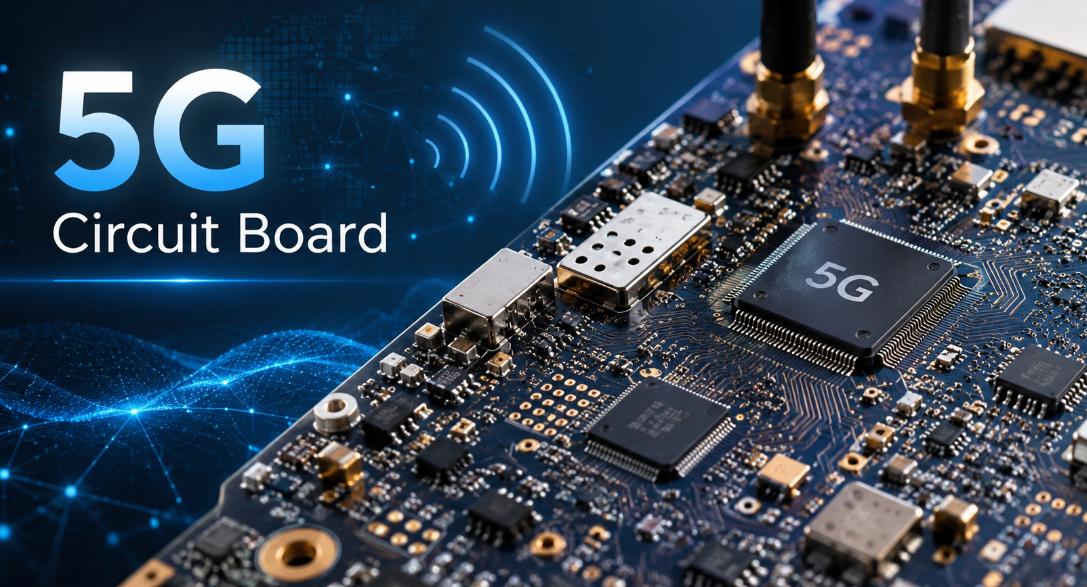
A 5G circuit board supports RF signals, digital control, power paths, antenna modules, and high-speed data transmission. It requires tighter control of signal loss, impedance, heat, and interference than a standard PCB.

A 5G printed circuit board may use rigid PCB, HDI PCB, flexible PCB, rigid-flex PCB, high-frequency PCB, or hybrid stack-up.
The final structure depends on frequency band, antenna layout, signal path, assembly density, power level, and reliability target.

What Materials Are Used for 5G Circuit Boards?

Material choice affects RF loss, impedance stability, heat control, and PCB reliability. The right laminate should match frequency, stack-up, power level, and assembly method.

Material choice affects signal loss, impedance stability, thermal behavior, and PCB reliability.
High-Tg FR4 can support control circuits and lower-frequency areas.
Low-loss materials are better for RF paths, antenna sections, microwave circuits, and high-speed communication layers.

MaterialTypical UseKey ValueCommon Range
High-Tg FR4Control circuitCost controlTg 150–180°C
RogersRF pathLow lossDk 2.2–3.5
PTFEMicrowave areaStable dielectricDk 2.1–2.9
Hydrocarbon ceramicAntenna/RFLow DfDf 0.001–0.004
LCPFlexible RFLow moistureDk 2.9–3.2
Hybrid stack-upMixed circuitsBalanced cost4–20 layers

What Are the Main Types of 5G Circuit Boards?

Different 5G products require different PCB structures. The right type depends on RF performance, routing density, bending demand, product size, and assembly requirements.

Main 5G circuit board types include high-frequency PCB, HDI PCB, multilayer PCB, flexible PCB, and rigid-flex PCB.
Each type fits different product structures, RF requirements, assembly density, and space limits.

  • High-frequency PCB: Used for RF transmission, antenna paths, filters, and microwave circuits.
  • HDI PCB: Used for compact 5G modules with fine-pitch components and dense routing.
  • Multilayer PCB: Used for boards that combine RF, digital, power, and control circuits.
  • 5G flexible circuit boards: Used for antenna connections, compact wireless devices, and bendable structures.
  • Rigid-flex PCB: Used for folding structures, space-saving layouts, and stable interconnects.

Where Are 5G Circuit Boards Commonly Used?

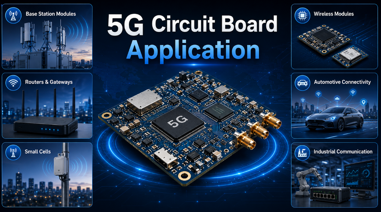
5G circuit boards are used in products that require stable wireless signal, compact layout, and reliable assembly. Common areas include telecom, wireless modules, automotive connectivity, and industrial communication.

  • Base station modules: RF boards, antenna boards, power boards, and control boards.
  • Routers and gateways: High-speed wireless communication products.
  • Small cells: Compact indoor or urban 5G coverage devices.
  • Wireless modules: IoT, tracking, monitoring, and communication modules.
  • Automotive connectivity: V2X modules, telematics, and wireless control units.
  • Industrial communication devices: Remote monitoring, wireless control, and smart equipment.
5G Circuit Board Application, https://www.bestpcbs.com/blog/2026/06/5g-circuit-board/

What Are the Technical Requirements for 5G Circuit Boards?

A reliable 5G circuit board depends on controlled impedance, low-loss material, stable stack-up, thermal control, fine routing, and suitable surface finish.

Core requirements include impedance control, low-loss material, stable stack-up, thermal control, fine routing, and reliable finish.

ItemRecommended Control
Impedance tolerance±5% to ±10%
RF line widthBased on stack-up
Minimum line/space3/3 mil or tighter
Layer count4–20+ layers
Copper thickness0.5–3 oz
Surface finishENIG, ENEPIG, immersion silver
Via typeThrough, blind, buried, back-drilled
Thermal rangeProduct class
TestingE-test, AOI, impedance test

How to Design a 5G Circuit Board for High-Frequency Performance?

Good 5G circuit board design starts with frequency, stack-up, material, impedance, grounding, routing, vias, and heat control. These items should be reviewed before prototype production.
Design must control frequency, stack-up, material, impedance, RF routing, grounding, vias, and thermal management.

  • Confirm the working frequency first: This guides laminate choice, trace geometry, connector type, and antenna clearance.
  • Define the stack-up early: Control dielectric thickness, copper weight, layer order, and reference planes.
  • Choose the right PCB material: Use FR4 for control circuits and low-loss laminates for RF paths.
  • Control impedance: Match trace width, spacing, dielectric height, copper thickness, and solder mask rules.
  • Keep RF routing clean and short: Avoid unnecessary bends, stubs, vias, and sudden width changes.
  • Protect the reference ground plane: Continuous ground improves return current and reduces noise.
  • Manage via structure carefully: Use blind vias, buried vias, back-drilling, or via-in-pad only when required.
  • Separate RF, digital, and power sections: Use spacing, shielding, and grounding to reduce interference.
  • Plan heat dissipation early: Power amplifiers and RF modules require stable thermal paths.
  • Check DFM before fabrication: Confirm line width, spacing, holes, annular ring, solder mask, and panelization.

How Does the 5G Circuit Board Manufacturing Process Work?

The manufacturing process turns design files into a functional high-frequency PCB. For 5G PCB production, material control, copper quality, via reliability, and impedance consistency are critical.

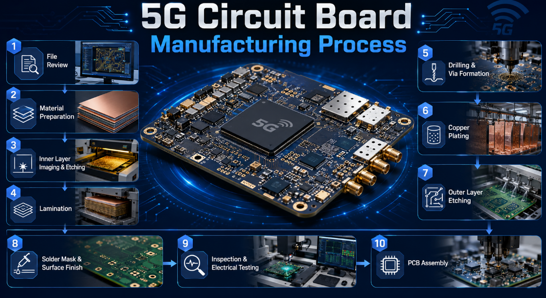
Step-by-step process for 5G PCB production:

1. File review: Check Gerber, drill files, stack-up, impedance notes, BOM, placement files, and test requirements.

2. Material preparation: Prepare FR4, high-Tg FR4, Rogers, PTFE, LCP, or hybrid laminates; check batch, thickness, and copper foil.

3. Inner layer imaging and etching: Form inner circuits; control line width, spacing, copper balance, and registration.

4. Lamination: Press inner layers, prepreg, and copper foil to form multilayer stack-up; control pressure and temperature.

5. Drilling and via formation: Mechanical or laser drilling, blind/buried vias, back-drilling; ensure hole quality.

6. Copper plating: Plate through holes and via walls; check plating thickness and uniformity.

7. Outer layer imaging and etching: Form outer circuit; control trace width and spacing for RF paths.

8. Solder mask and surface finish: Apply solder mask and finish, such as ENIG, ENEPIG, or immersion silver.

9. Inspection and electrical testing: Use AOI, E-test, impedance coupon test, visual check, and dimension inspection.

10. PCB assembly if required: SMT, DIP, solder paste printing, component placement, reflow, AOI, X-ray, cleaning, and functional testing.

5G Circuit Board Manufacturing Process, https://www.bestpcbs.com/blog/2026/06/5g-circuit-board/

What Should Be Confirmed Before 5G Circuit Board Assembly?

Before assembly starts, BOM, placement file, polarity, RF components, soldering plan, inspection method, and testing requirements should be confirmed to reduce SMT errors and rework.

Confirm BOM, placement, polarity, RF components, solder paste, inspection, and test plan.

  • BOM: Part number, value, package, brand, tolerance, and alternatives.
  • Placement file: X/Y location, rotation, side, and reference designator.
  • RF components: Connectors, filters, amplifiers, shielding.
  • Polarity notes: Diodes, LEDs, ICs, tantalum capacitors.
  • PCB finish: ENIG, ENEPIG.
  • Soldering plan: Paste type, stencil thickness, reflow profile.
  • Inspection method: AOI, X-ray, visual, impedance, functional.
  • Special requirements: Shielding, programming, labeling, cleaning, conformal coating, packaging, fixture testing.

Why Choose EBest as Your 5G Circuit Board Manufacturer?

A strong 5G circuit board manufacturer should support material selection, design review, PCB fabrication, assembly, testing, and delivery in one clear workflow. EBest helps reduce communication gaps and production risk.

EBest helps reduce 5G circuit board project risk by combining material selection, design review, prototype validation, PCB fabrication, assembly, and inspection in one workflow.

With over 20 years of experience, EBest supports high-frequency PCB, HDI PCB, flexible PCB, rigid-flex PCB, RF PCB, and impedance control PCB projects. This provides clearer technical review, smoother production handoff, stable quality control, and faster quotation response.

  • Comprehensive PCB capabilities: FR4, multi-layer, metal-core, ceramic, semi-rigid flex, HDI, high-Tg, heavy copper, impedance control PCBs.
  • Expedited service: Urgent boards can be completed and shipped within 24 hours.
  • Strict quality certifications: IATF 16949, ISO 9001, ISO 13485, AS9100D, RoHS, REACH, UL.
  • Customized solutions: Personalized support, DFM review, material selection, and design verification.
  • Turnkey project support: End-to-end oversight from design review, prototype, fabrication, assembly, and functional testing.
5G Circuit Board, https://www.bestpcbs.com/blog/2026/06/5g-circuit-board/

Case Study: 5G Tower Circuit Board Project

This 5G tower circuit board project required stable RF performance, controlled impedance, thermal control, shielding, and reliable assembly. EBest managed the project from file review to prototype validation and batch production.
  • Project Background: A telecom provider needed a high-frequency 5G tower PCB integrating RF, antenna, power, and digital circuits.
  • Project Requirements: Stable RF, low insertion loss, controlled impedance, thermal management, SMT and through-hole assembly, shielding, functional testing.
  • Challenges: Complex multilayer stack-up, impedance ±5% tolerance, dense component placement, coordination of fabrication and assembly.
  • EBest Solutions: Full file review, low-loss laminate selection, prototype validation, integrated PCB fabrication and assembly, strict QC inspections.
  • Results: Prototype met RF, thermal, and assembly requirements; mass production achieved high yield and repeatable quality; on-time delivery with minimal revisions.

FAQs About 5G Circuit Boards

Q1: What file package is needed for a quote?
A1: Gerber, drill files, stack-up, impedance notes, BOM, placement file, assembly drawing, and test instructions.

Q2: Which materials are suitable for high-frequency 5G PCBs?
A2: Rogers, PTFE, LCP, hybrid stack-ups, and high-Tg FR4.

Q3: What inspections does EBest provide?
A3: AOI, X-ray, E-test, impedance testing, visual inspection, and functional testing.

Q4: Can EBest handle both prototype and volume production?
A4: Yes. Small-batch prototypes, pilot runs, and mass production are supported.

Q5: How is impedance controlled?
A5: Through stack-up design, trace width, spacing, dielectric thickness, copper thickness, and test coupons.

Q6: What is the typical layer count?
A6: 4–20+ layers, depending on RF routing, shielding, and component density.

Q7: What affects 5G circuit board cost most?
A7: Material type, layer count, impedance, copper thickness, via structure, surface finish, assembly scope, and testing requirements.

Get a Fast Quote for Your 5G Circuit Board Project

A clear quote starts with complete project files. Send Gerber, BOM, stack-up, impedance notes, and test requirements to EBest for fast review and practical production feedback.

EBest Circuit provides customized, high-frequency 5G PCB solutions from design review to turnkey delivery. Ensure your project meets RF, thermal, and assembly requirements efficiently. Contact us now at sales@bestpcbs.com to get a fast, accurate quote and professional support from concept to delivery.

You may also like

LED Lighting PCB Manufacturer

June 12th, 2026

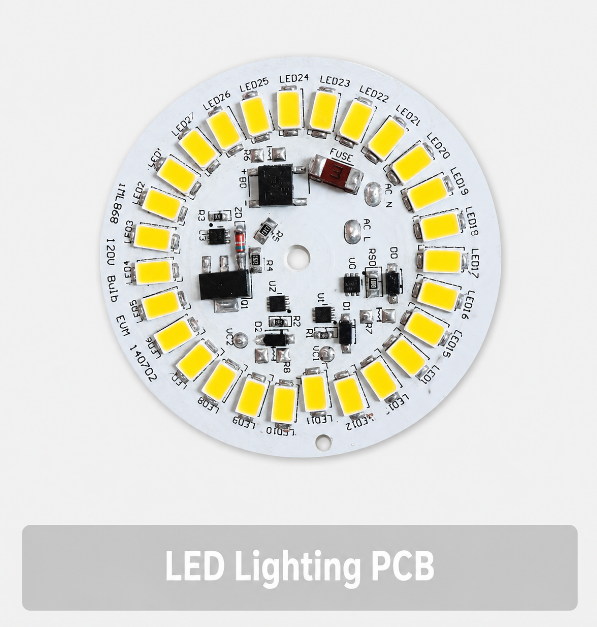
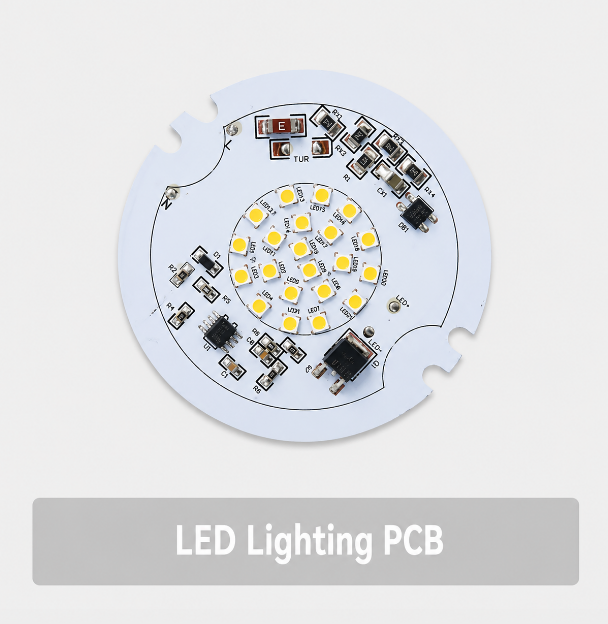
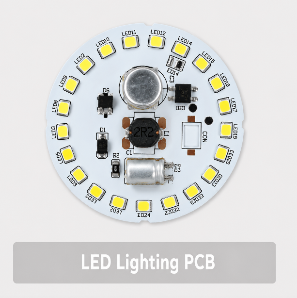
LED Lighting PCB provides electrical connection, mechanical support, and heat dissipation for LED modules. EBest Circuit manufactures custom LED Lighting PCB using aluminum PCB, FR4 PCB, and turnkey assembly services for residential, commercial, high-power, automotive, and outdoor lighting projects.

Are you worried about these problems in LED Lighting PCB projects?

  • Delivery delays: Unstable production cycles, slow sample approval, material shortages, or batch delays may disrupt your project schedule.
  • Hidden costs: Extra charges may appear after quotation approval, including tooling changes, material upgrades, testing fees, or assembly adjustments.
  • Quality instability: Batch variation may cause flickering, overheating, soldering defects, color inconsistency, or field failure risks.

As a 20+ years PCB manufacturer, EBest Circuit provides manufacturing and assembly solutions for global lighting brands, OEM factories, and engineering projects.

  • Delivery predictability: ERP + MES production tracking supports 7-day standard delivery, 48-hour urgent response, and delay rate controlled at ≤2%.
  • Cost transparency: BOM-level cost modeling locks pricing before production and covers material, fabrication, assembly, testing, packaging, and export documentation.
  • Quality reliability: AOI inspection, flying probe testing, thermal validation, and functional testing support 100% critical process inspection, ≤0.3% defect rate, and ≥98% batch consistency.

Welcome to contact us if you have any request for LED lighting PCB manufacturing and assembly: sales@bestpcbs.com.

What Is an LED Lighting PCB?

An LED lighting PCB is a printed circuit board used to mount, connect, and power LED components in lighting products. It provides current paths, mechanical support, thermal transfer, and assembly stability for LED modules.

Unlike standard circuit boards, LED lighting boards must handle heat, current load, brightness stability, and long operating hours. Poor PCB quality may cause hot spots, unstable light output, solder joint fatigue, and early LED failure.

EBest Circuit manufactures custom LED PCB, aluminum PCB, FR4 PCB, and assembled LED modules for residential, commercial, industrial, automotive, and outdoor lighting applications.

Why Do LED Lighting Products Need Reliable PCB Solutions?

LED lighting products rely on stable PCB performance because heat, current, and soldering quality directly affect lifespan. A weak PCB may reduce brightness, increase failure rates, and raise after-sales cost.

Reliable PCB solutions help control:

  • Thermal stability: Better heat transfer reduces LED junction temperature.
  • Electrical safety: Stable copper design supports consistent current flow.
  • Assembly yield: Accurate pads and solder mask control reduce SMT defects.
  • Batch consistency: Controlled fabrication keeps repeated orders stable.
  • Long-term reliability: Better materials reduce delamination, oxidation, and early failure.

Choosing the right manufacturer affects warranty risk, brand reputation, and total project cost.

What LED Lighting PCB Types Can We Manufacture?

EBest Circuit manufactures LED lighting boards according to power level, heat dissipation demand, product structure, and assembly requirements. Instead of using one fixed PCB type, we help customers choose the right structure for actual working conditions.

Common PCB types include:

  • Aluminum LED PCB: Suitable for high-power LED modules, street lights, flood lights, panel lights, and outdoor lighting products.
  • FR4 LED PCB: Suitable for low-power and medium-power residential lighting, commercial lighting, control circuits, and cost-sensitive products.
  • Metal Core PCB: Designed for products that require stronger thermal performance, stable mechanical support, and long operating life.
  • Heavy Copper LED PCB: Used for products with higher current load, stronger power demand, or long continuous operation.
  • High TG LED PCB: Suitable for lighting products exposed to higher working temperature or repeated thermal stress.
  • Multilayer LED PCB: Used when modules include driver circuits, control functions, sensors, communication modules, or compact routing.
  • Flexible and Rigid-Flex LED PCB: Suitable for curved lighting structures, automotive lighting, wearable lighting, compact modules, and special installation spaces.

The right type should match LED power, thermal path, fixture housing, installation environment, and production cost.

Aluminum PCB vs FR4 PCB for LED Lighting

Aluminum PCB and FR4 PCB solve different lighting problems. The choice affects heat dissipation, electrical stability, product cost, assembly yield, and long-term reliability.

ItemAluminum PCBFR4 PCB
Thermal Conductivity1.0–3.0 W/m·K0.3–0.5 W/m·K
Copper Thickness1oz–3oz1oz–2oz
Best UseHigh-power LEDLow to medium-power LED
Heat ControlStrongLimited
CostHigherLower
ApplicationsStreet light, flood light, panel lightIndoor lamp, control PCB, low-power module

Aluminum PCB is better for high-power LED lighting because it transfers heat away from LED components more efficiently. This helps reduce hot spots, solder joint stress, brightness decay, and early failure.

FR4 PCB is better for low-power LED lighting where heat is easier to control. It is often used in indoor lamps, control boards, small LED modules, and commercial lighting products where cost control matters more than extreme thermal performance.

From a project cost view, aluminum PCB is usually more expensive because the material and processing requirements are higher. However, for street lights, flood lights, grow lights, and high-power modules, better heat dissipation can reduce field failure and after-sales cost.

FR4 PCB is practical when the LED current is lower, the fixture has a separate heat sink, or the board mainly supports control functions. It can reduce material cost, simplify production, and support multilayer routing more easily.

In short, choose aluminum PCB for high-heat lighting products and choose FR4 PCB for low-power or cost-sensitive lighting applications.

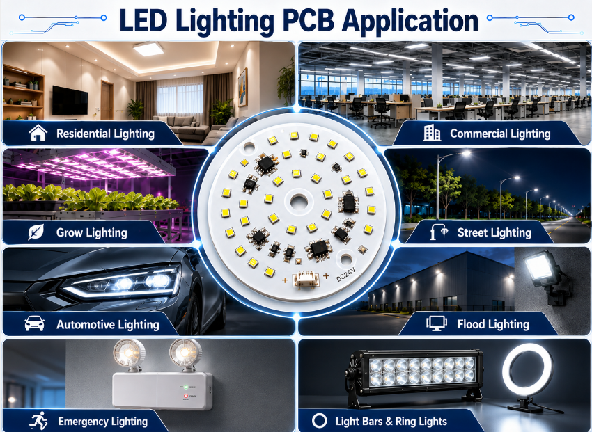
LED Lighting PCB Applications We Support

LED lighting boards are used in many lighting products, and each application has different priorities. Outdoor lighting focuses on heat, waterproof structure, and long service life. Indoor lighting focuses on cost, shape, brightness consistency, and assembly efficiency.

EBest Circuit supports PCB for:

  • Residential lighting: Ceiling lights, downlights, panel lights, and indoor lamps.
  • Commercial lighting: Office lighting, retail lighting, warehouse lighting, and display lighting.
  • Street lighting: High-power street light modules and aluminum PCB solutions.
  • Flood lighting: High-brightness PCB for outdoor and industrial lighting.
  • Grow lighting: Stable current and heat control for horticultural lighting.
  • Automotive lighting: Vehicle lamps, signal lights, and interior lighting.
  • Emergency lighting: Backup lighting systems and emergency light circuit boards.
  • Light bars and ring lights: Custom-shaped boards for compact lighting products.

For each application, we match material, copper thickness, LED layout, and assembly process to the final product structure.

LED Lighting PCB Applications

How Do We Improve Heat Dissipation for LED PCB?

Heat dissipation directly affects brightness stability, color consistency, solder joint life, and product lifespan. If heat is not controlled, LEDs may suffer brightness drop, color shift, solder fatigue, and early failure.

EBest Circuit improves thermal performance through:

  • Aluminum substrate selection: Aluminum PCB improves heat transfer for high-power LED modules.
  • Copper thickness optimization: 1oz, 2oz, or thicker copper supports current flow and heat spreading.
  • Thermal pad control: Proper LED pad design improves heat transfer from LED packages.
  • LED spacing optimization: Correct spacing reduces local hot spots and uneven heating.
  • Surface finish control: HASL and ENIG are selected based on soldering and reliability needs.
  • Thermal testing: Temperature rise is checked during sample validation and production testing.

For high-power projects, aluminum PCB, suitable copper thickness, and fixture-level thermal review are recommended before mass production.
What LED Lighting PCB Assembly Services Do We Provide?

EBest Circuit provides assembly services from bare PCB fabrication to finished LED modules. This helps customers reduce supplier coordination, shorten project cycles, and control quality from one source.

Assembly services include:

  • SMT assembly: For 2835, 5730, 3030, 5050, COB-related components, and LED driver parts.
  • Through-hole assembly: For connectors, terminals, switches, and power components.
  • Mixed assembly: For boards with both SMD and through-hole components.
  • Functional testing: Voltage, current, brightness, polarity, and continuity checks.
  • Turnkey service: PCB fabrication, component sourcing, assembly, testing, and packaging.

This service supports lighting brands, product developers, and OEM lighting manufacturers.

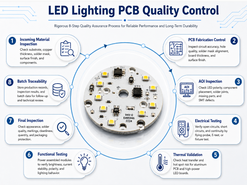
How Do We Control LED Lighting PCB Quality?

EBest Circuit controls quality from material inspection to final function testing. Each step reduces overheating, soldering defects, electrical failure, and batch inconsistency.

  • Incoming material inspection: We check substrate, copper thickness, solder mask, surface finish, and components before production.
  • PCB fabrication control: We inspect circuit accuracy, hole quality, solder mask alignment, board thickness, and surface finish.
  • AOI inspection: Automated optical inspection checks LED polarity, component placement, solder joints, missing parts, and visible SMT defects.
  • Electrical testing: Flying probe testing, E-test, or fixture testing checks open circuits, short circuits, and continuity.
  • Thermal validation: Aluminum PCB and high-power LED boards are checked for heat transfer and hot spot risk.
  • Functional testing: Assembled modules are powered under working voltage to verify brightness, current stability, polarity, and lighting behavior.
  • Final inspection: Board appearance, solder quality, markings, cleanliness, quantity, and packaging protection are checked before shipment.
  • Batch traceability: Production records, inspection results, and batch data are stored for follow-up and technical review.
LED Lighting PCB Quality Control

How Can We Help Optimize LED Light PCB Cost?

Cost optimization is not about choosing the cheapest board. It is about reducing unnecessary cost while keeping thermal performance, electrical stability, assembly yield, and long-term reliability under control.

Best Technology helps optimize cost through early engineering review, material selection, BOM checking, and production planning.

  • Choose the right material: Use aluminum PCB for high-heat products and FR4 PCB for low-power indoor lighting to avoid over-specification.
  • Optimize copper thickness: Select suitable copper weight based on current load and heat spreading. Too much copper increases cost, while too little copper increases heat risk.
  • Improve PCB size and panel utilization: Review board outline, spacing, and panel layout to reduce material waste and improve production efficiency.
  • Review LED layout before production: Proper spacing reduces hot spots, improves light uniformity, and avoids redesign after sampling.
  • Control BOM cost: Review LEDs, resistors, connectors, drivers, and other parts to find stable, cost-effective alternatives.
  • Reduce assembly defects: DFM review helps avoid solder bridging, wrong pad size, poor polarity marking, and SMT rework.
  • Verify prototype before mass production: Sample testing confirms thermal performance, brightness, current stability, and assembly quality.
  • Optimize order quantity: Proper batch planning reduces setup cost, material waste, packaging cost, and shipping cost per unit.

The final goal is stable LED performance, predictable delivery, and reliable mass production at a controlled total cost.

Case Study: High-Power LED Street Light PCB Project

Project Background
A European lighting customer was developing a high-power LED street light for city roads and industrial areas. Their previous supplier had unstable delivery, uneven batch quality, and poor heat dissipation, causing fixture assembly delays and higher project risk.

Project Requirements

  • Quantity: 5,000 high-power LED boards for outdoor street lighting.
  • Power: Support LED modules above 100W.
  • Material: Use aluminum PCB or high thermal conductivity material.
  • Quality: Control defect rate at ≤0.3% and batch consistency at ≥98%.
  • Compliance: Meet RoHS requirements.
  • Performance: Keep uniform light output, stable electrical performance, and long-term operation.
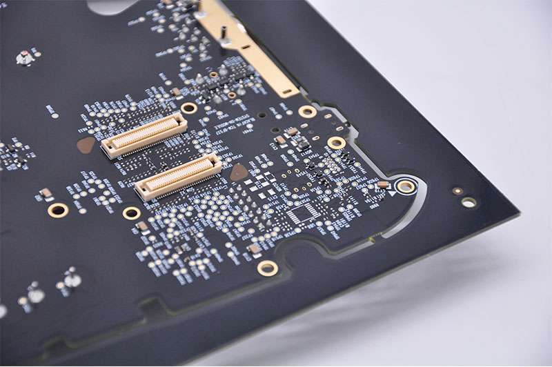
Project Solution

  • PCB structure optimization: Use 2oz aluminum PCB for better current capacity and heat spreading.
  • LED layout improvement: Adjust LED spacing and copper distribution to reduce hot spots and improve light uniformity.
  • Thermal management: Use high thermal conductivity aluminum substrate and optimized thermal paths.
  • Assembly control: Apply AOI inspection, electrical testing, thermal validation, and functional testing during production.
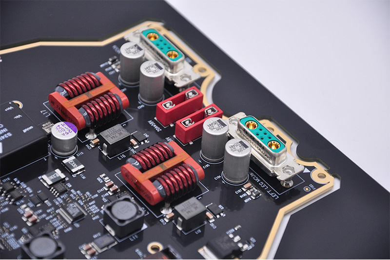
  • Delivery management: Use ERP + MES tracking to control schedule and reduce delivery uncertainty.

Project Results

  • On-time delivery: All 5,000 pieces were completed and shipped on schedule.
  • Stable thermal performance: Hot spot temperature was controlled below 45°C under defined test conditions.
  • Consistent quality: Batch consistency reached ≥98%, and defect rate was controlled at ≤0.3%.
  • Customer approval: The customer approved mass production and continued cooperation on related street light and flood light projects.

This project shows how Best Technology helps customers solve delivery, heat dissipation, and batch quality problems through proper material selection, production control, and full-process testing.

High-Power LED Street Light PCB

Why Choose EBest as Your LED Lighting PCB Manufacturer?

EBest Circuit, also known as Best Technology, is a China source PCB manufacturer with 20+ years of experience. We provide one-stop solutions from design support, prototype, and mass production to component sourcing, assembly, testing, and global delivery.

Here are reasons why choose EBest as your LED lighting PCB manufacturer:

  • Experienced manufacturer: 20+ years of PCB manufacturing experience reduces production risk.
  • One-stop service: Design support, prototype, mass production, sourcing, assembly, and testing are handled by one supplier.
  • Diverse PCB options: FR4, aluminum, metal core, heavy copper, high TG, multilayer, and impedance control PCB are available.
  • Strong production capacity: Monthly capability reaches 260,000 sq. ft / 28,900 sq. m, with 1,000+ boards completed monthly.
  • Fast delivery: Expedited boards can be shipped within 24 hours when project conditions allow.
  • Certified quality: IATF 16949, ISO 9001:2015, ISO 13485:2016, AS9100D, REACH, RoHS, and UL are supported.
  • Global supply: China source factory supply with worldwide shipping and export documentation.
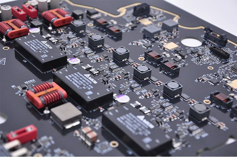
  • Cost transparency: BOM-level cost planning helps lock total project cost before production.
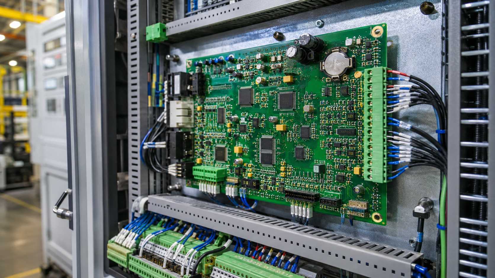
  • Reliable quality: Critical processes are inspected, with defect rate controlled at ≤0.3% and batch consistency reaching ≥98%.
  • Custom project support: OEM and ODM services support residential, commercial, automotive, street light, flood light, grow light, and emergency lighting projects.

FAQs About LED Lighting PCB

Q1: What copper thickness is common for LED lighting PCB?
A1: Common copper thickness includes 1oz, 2oz, and 3oz. For high-power modules, 2oz copper is often used to improve current capacity and heat spreading.

Q2: What thermal conductivity is suitable for aluminum PCB?
A2: Common aluminum PCB thermal conductivity is 1.0–3.0 W/m·K. Higher thermal conductivity is better for high-power lighting with stronger heat output.

Q3: Can LED PCB be custom-shaped?
A3: Yes. Boards can be made in round, ring, bar, square, panel, or irregular shapes according to fixture structure and mounting requirements.

Q4: What surface finishes are common?
A4: HASL and ENIG are common. ENIG provides flatter pads and better solderability, especially for higher-reliability assembly projects.

Q5: Can you assemble 2835 and 5730 LEDs?
A5: Yes. We support 2835, 5730, 3030, 5050, and other standard SMD LED packages based on BOM and placement files.

Q6: What files are needed for quotation?
A6: Recommended files include Gerber, BOM, pick-and-place file, quantity, material, copper thickness, surface finish, and testing requirements.

Q7: How can I reduce LED PCB cost?
A7: Cost can be reduced by optimizing panel usage, material selection, copper thickness, BOM, DFM, and order quantity before production.
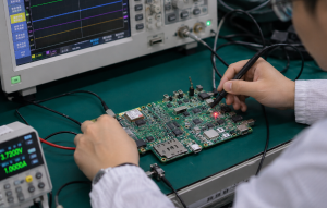
Q8: What causes LED PCB overheating?
A8: Common causes include poor thermal path, thin copper, dense LED spacing, weak substrate, or insufficient fixture-level cooling.

Q9: Do you provide prototypes?
A9: Yes. Prototypes help verify thermal performance, electrical stability, LED layout, brightness behavior, and assembly quality before mass production.

Q10: What is the typical lead time?
A10: Standard PCB orders can be completed in about 7 working days. Assembly lead time depends on BOM availability, quantity, and testing requirements.

Q11: Do you support outdoor LED projects?
A11: Yes. We support street lights, flood lights, grow lights, emergency lights, and other outdoor lighting products.

Q12: Can one order include aluminum and FR4 PCB?
A12: Yes. One project can include aluminum PCB for LED power modules and FR4 PCB for control circuits.

Q13: What defect rate is achievable?
A13: Under defined quality criteria, defect rate can be controlled at ≤0.3%, with batch consistency reaching ≥98%.

Q14: Do you provide global delivery?
A14: Yes. We support worldwide delivery by air, sea, or express, based on project urgency and order volume.

Q15: Can you review LED PCB design before production?
A15: Yes. We can review Gerber files, copper width, thermal path, panelization, pad design, and assembly risks before production.
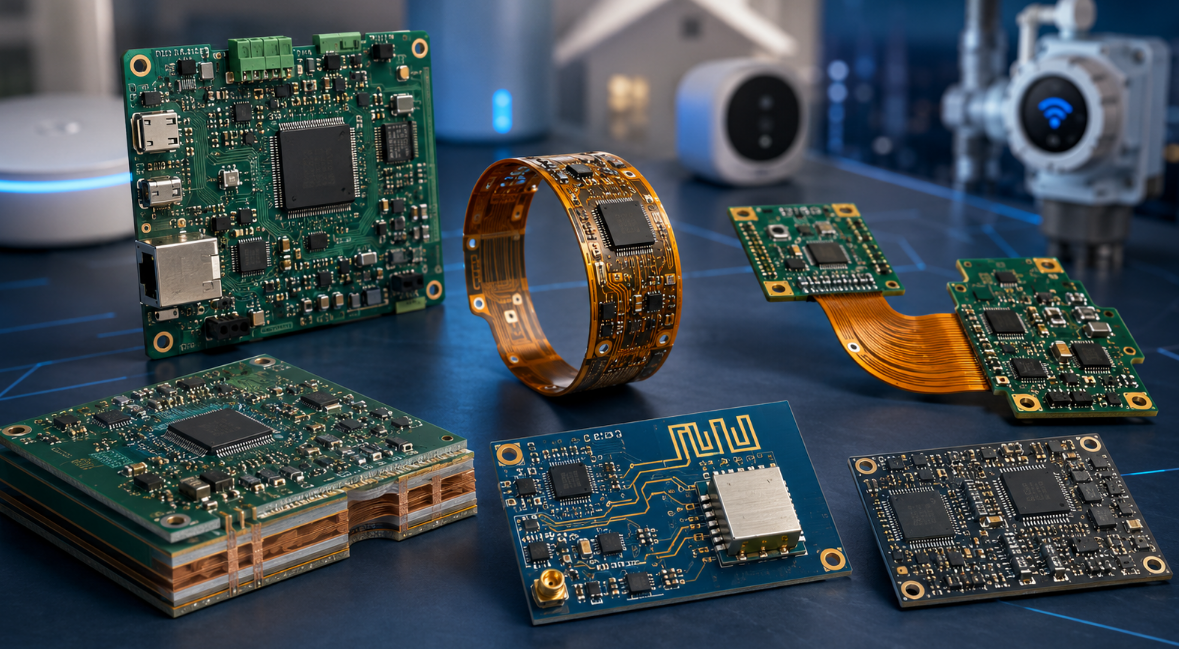
Request a Quote for Your LED Lighting PCB Project

LED lighting PCB performance depends on material selection, heat dissipation, copper design, solder quality, and batch control. Aluminum PCB is suitable for high-power lighting, while FR4 PCB is practical for cost-sensitive indoor lighting.

For procurement, buyers should evaluate delivery stability, quality traceability, testing capability, material selection, and total project cost, not only unit price. EBest Circuit offers custom manufacturing, assembly, cost review, quality inspection, and global delivery from China.

Send your Gerber files, BOM, quantity, material requirement, and assembly details to sales@bestpcbs.com for a fast LED lighting PCB quotation.

You may also like

Reliable Industrial Control PCB Manufacturer with Early DFM Review

June 11th, 2026

Industrial Control PCB is a printed circuit board designed for automation equipment, industrial controllers, PLC modules, control panels, temperature control systems, and other factory control devices. This article explains how EBest Circuit (Best Technology) supports Industrial Control PCB projects with early DFM review, PCB fabrication, material matching, industrial PCBA support, and manufacturing risk control.

What problems do OEM buyers often face when sourcing Industrial Control PCB projects?

  • Incomplete files: Gerber, stack-up, drill, BOM, or test notes are missing.
  • Wrong PCB type: FR4, multilayer, HDI, flexible PCB, or metal base options are not confirmed.
  • Hidden production risk: Hole size, copper thickness, impedance, or solder mask rules are ignored.
  • PCBA handoff issues: PCB fabrication and industrial control PCB assembly are handled separately.
  • Unclear quotation: Industrial control PCB quotes vary because suppliers review different details.

EBEST reduces these risks through early engineering review and practical manufacturing support.

  • File check: We review Gerber, drill, stack-up, material, copper, and test notes before production.
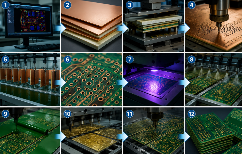
  • PCB matching: We help match FR4, high-Tg FR4, multi-layer PCB, HDI printed circuit board, flexible PCB, or metal core PCB.
  • Process review: We check copper weight, line width, spacing, holes, impedance, solder mask, and finish.
  • PCBA support: We can add BOM review, SMT, DIP, AOI, X-ray when required, and customer-defined testing.
  • Clearer quote: We quote based on real manufacturability, not just board size and quantity.

​EBest Circuit (Best Technology) is a China industrial control PCB and PCBA manufacturer supporting industrial control FR4 PCB fabrication, industrial control PCBA, early DFM review, and turnkey project delivery. Our standard PCB capabilities include 1–50 layers, FR4 Tg 130–180 materials, 0.4–6.0 mm standard board thickness, FR4 inner copper from 0.5 oz to 6 oz, FR4 outer copper from 0.5 oz to 10 oz, controlled impedance, ENIG, ENEPIG, HASL, OSP, immersion tin, immersion silver, hard gold, soft gold, carbon ink, and gold finger plating. For industrial control PCB quotes, please send your Gerber files, stack-up, BOM, assembly drawing, copper thickness, surface finish, testing requirements, quantity, and delivery target to sales@bestpcbs.com.

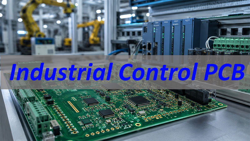
Industrial Control PCB

What Should OEM Buyers Confirm Before Starting an Industrial Control PCB Project?

Industrial Control PCB projects should start with clear application and manufacturing requirements. This helps EBEST review whether the design can be built, assembled, tested, and repeated without unnecessary delays.

OEM buyers should confirm the following points before asking for industrial control PCB pricelist​:

  • Product use: PLC, control panel, motor control, sensor module, or temperature controller.
  • PCB type: FR4, multilayer, HDI, flexible PCB, metal base, or high-frequency PCB.
  • Board structure: Layer count, board thickness, copper weight, and stack-up.
  • Reliability needs: Tg, impedance, surface finish, solder mask, and testing method.
  • PCBA scope: Bare PCB only or PCB industrial controller assembly.

For example, a simple SMD PCB for industrial controller use may need standard FR4 and ENIG. A high-density PCB for industrial control systems may need finer line width, smaller vias, HDI structure, or controlled impedance. A control panel board with connectors and terminals may need stronger mechanical review and stable DIP assembly.

EBEST asks these questions early because industrial control boards often stay in production for years. A weak starting review can lead to repeat quotation changes, assembly problems, or unstable batch quality.

A clear project start gives the buyer a faster quote and gives the factory a better chance to control risk.

How Does EBEST Review Industrial Control PCB Files Before Production?

EBEST reviews Industrial Control PCB files before production to catch risks that may not be obvious from the board outline. The goal is not to slow the project down, but to prevent avoidable problems before fabrication and assembly.

Our early DFM review usually covers:

  • Gerber and drill file completeness
  • Layer count and stack-up
  • FR4 Tg requirement
  • Board thickness and tolerance
  • Inner and outer copper weight
  • Minimum line width and spacing
  • Minimum mechanical hole size
  • PTH and NPTH hole tolerance
  • Impedance requirement
  • Solder mask bridge and opening
  • Surface finish
  • Panelization and V-CUT design
  • Gold finger or edge connector area
  • BOM and assembly files if PCBA is required

EBEST’s standard PCB capability supports 1–50 layers and standard board thickness from 0.4 mm to 6.0 mm. For special projects, thinner, thicker, or higher-layer structures can be reviewed separately. This matters for industrial control system PCB projects because thick boards, dense routing, connectors, and repeated plugging can affect manufacturability.

For controlled impedance designs, EBEST reviews the stack-up, copper thickness, trace width, spacing, and impedance notes together. Our standard impedance tolerance is ±5Ω for impedance below 50Ω and ±10% for impedance of 50Ω or above.

A useful DFM review should tell the buyer what can be produced, what needs adjustment, and what may affect cost or lead time.

Which PCB Type Fits Industrial Control Applications?

Industrial control applications do not all use the same PCB type because signal density, current load, heat, space, and assembly needs are different.

EBEST can review the PCB type based on the actual control system.

Common options include:

  • FR4 PCB: Suitable for standard control boards, I/O modules, sensor interfaces, and general industrial controller circuits.
  • High-Tg FR4 PCB: Used for boards that need better heat resistance during assembly or long-term operation.
  • Multilayer PCB: Suitable for PLC modules, automation controllers, and dense industrial control system PCB designs.
  • HDI PCB: Used for compact controllers that need smaller vias, higher routing density, or limited board space.
  • Flexible PCB / Rigid-Flex PCB: Suitable for moving parts, compact wiring, vibration-sensitive modules, or reduced connector use.
  • Aluminum PCB: Used for LED industrial modules, thermal control areas, or power sections that need better heat spreading.
  • High-Frequency PCB: Suitable for industrial communication modules or control boards using RF or low-loss materials.

EBEST supports FR4 Tg 130–180 materials and can also review Rogers, Taconic, Arlon, Nelco, and other specified materials when required.

The best PCB type is the one that fits the product’s current, heat, density, reliability, and assembly needs.

How Does EBEST Manufacture FR4 and Multilayer PCB for Industrial Controllers?

FR4 and multilayer PCB are common choices for industrial controllers because they support stable routing, controlled cost, and long-term manufacturability. EBEST manufactures these boards by reviewing material, copper, layer count, drilling, solder mask, and surface finish before production.
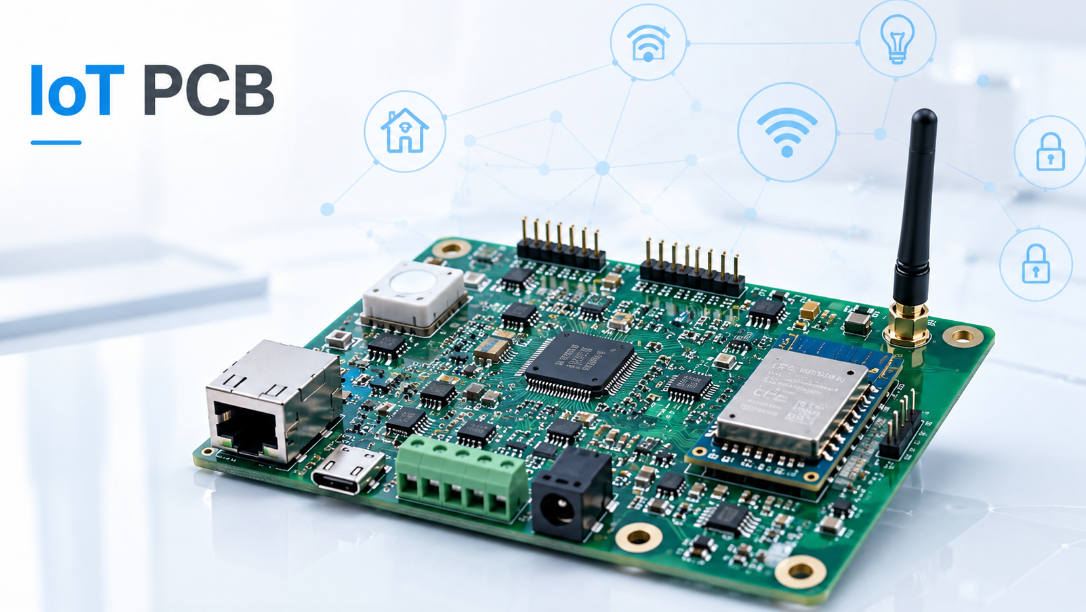
For industrial controller PCB projects, EBEST can support:

  • 1–50 layer standard PCB production
  • FR4 Tg 130–180 material options
  • Standard board thickness from 0.4 mm to 6.0 mm
  • FR4 inner copper from 0.5 oz to 6 oz
  • FR4 outer copper from 0.5 oz to 10 oz
  • Mechanical finished hole size from 0.15 mm to 6.5 mm
  • Laser via minimum 0.10 mm under standard capability
  • Standard through-hole aspect ratio up to 12:1
  • Solder mask colors including green, black, blue, red, white, yellow, and others
  • Surface finishes including HASL, lead-free HASL, ENIG, ENEPIG, OSP, immersion tin, immersion silver, hard gold, and soft gold

For multilayer PCB for industrial controller projects, the stack-up is important. The material, copper distribution, dielectric thickness, via structure, and impedance requirement all affect both electrical performance and production stability.

For thick copper designs, line width and spacing must be reviewed together with copper weight. A 1 oz board cannot use the same routing rule as a 6 oz, 10 oz, or heavier copper board.

EBEST manufactures FR4 and multilayer industrial control PCB projects with process review first, so the final board is not only built, but built with repeatable rules.

What PCBA Support Can EBEST Add to Industrial Control PCB Projects?

Many industrial control projects do not stop at bare PCB fabrication. After the board is made, customers may still need industrial control PCB assembly, SMD assembly, DIP assembly, connector soldering, inspection, and functional test support.

EBEST can add PCBA support when the project needs a more complete manufacturing workflow:

  • BOM review and component sourcing review
  • SMT assembly for SMD PCB industrial controller projects
  • DIP assembly for connectors, relays, terminals, and large components
  • BGA/QFN assembly when required
  • AOI inspection
  • X-ray inspection when required
  • First article inspection
  • Customer-defined functional testing
  • Conformal coating or box-build support when required by the project

This is useful for industrial automation control panel PCB projects because these boards often include connectors, terminals, relays, communication ports, power input areas, and mixed SMT plus through-hole components.

If PCB fabrication and PCBA assembly are handled by different suppliers, the buyer may need to solve handoff issues alone. Common problems include incorrect component direction, unclear test points, poor connector fit, soldering difficulty, missing assembly notes, or late BOM changes.

EBEST’s value is to review the PCB and PCBA requirements together. This helps customers reduce repeated communication and improve project control from board fabrication to assembled controller board.

What Manufacturing Risks Should Industrial Control PCB Buyers Watch For?

Industrial Control PCB buyers should watch for manufacturing risks before the order enters production. Small details can become large problems when the board is used inside automation equipment or industrial controllers.
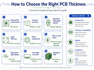
Common risks include:

  • Wrong material grade
    A low Tg material may not fit higher assembly or operating temperature needs.
  • Copper rule mismatch
    High copper weight needs wider line width and spacing.
  • Hole and board thickness conflict
    Small holes on thick boards may exceed practical aspect ratio limits.
  • Unclear impedance control
    Without stack-up and impedance notes, the supplier may not quote or build correctly.
  • Weak connector area
    Industrial control boards often need stable terminals, sockets, or gold finger contact areas.
  • Missing PCBA test plan
    Electrical testing does not replace functional testing for assembled control boards.

EBEST helps reduce these risks through early DFM review, process capability review, material confirmation, impedance review, surface finish review, PCBA planning, inspection, and customer-defined testing.

For example, if a buyer only asks for an industrial control PCB pricelist, the quote may miss key risks. A reliable industrial control PCB supplier should ask about the product use, board structure, copper weight, assembly scope, and test requirement.

The best supplier is not the one that gives the fastest price. It is the one that finds problems before production.

Industrial Control PCB Case: How Did EBEST Support an Automation Control Panel Project?

An OEM customer needed an Industrial Control PCB for an automation control panel used in factory equipment. The board was used inside an industrial controller module, requiring stable signal control, connector reliability, and smooth PCBA assembly.

EBEST supported the project through the following steps:

  • Application review: The PCB was reviewed based on its use in an automation control panel and industrial controller module.
  • PCB specification check: EBEST checked the 6-layer FR4 structure, Tg150 material, 1 oz inner and outer copper, 1.6 mm board thickness, and ENIG surface finish.
  • Production file review: Gerber files, stack-up, copper thickness, board thickness, BOM, assembly drawing, connector areas, test points, and functional test requirements were reviewed before production.
  • PCB and PCBA support: EBEST supported PCB fabrication, BOM review, SMT assembly, DIP connector assembly, AOI inspection, FAI, and customer-defined functional testing.
  • Customer value: The customer reduced handoff risk between PCB fabrication, assembly, inspection, and testing.

Key project parameters:

  • Application: Automation control panel PCB
  • Product use: Industrial controller module
  • PCB type: 6-layer FR4 PCB
  • Material Tg: Tg150
  • Copper thickness: 1 oz inner and outer copper
  • Board thickness: 1.6 mm ±10%
  • Solder mask / silkscreen: Green solder mask, white silkscreen
  • Surface finish: ENIG
  • Gold thickness: Au 1 μin
  • Assembly support: SMT assembly and DIP connector assembly
  • Inspection and testing: AOI, FAI, and customer-defined functional testing
Industrial Control PCB

FAQs About Industrial Control PCB

What Is an Industrial Control PCB?
An Industrial Control PCB is a printed circuit board used in automation equipment, PLC modules, control panels, industrial controllers, motor control units, temperature controllers, and factory control systems.

Can EBEST Support Industrial Control PCB Assembly?
Yes. EBEST can support industrial control PCB assembly with BOM review, component sourcing review, SMT assembly, DIP assembly, AOI inspection, X-ray inspection when required, FAI, and customer-defined functional testing.

What PCB Types Are Used in Industrial Control Systems?
Common options include FR4 PCB, high-Tg FR4 PCB, multilayer PCB, HDI PCB, flexible PCB, rigid-flex PCB, aluminum PCB, and high-frequency PCB.

What Files Should I Send for Industrial Control PCB Quotes?
Please send Gerber files, drill files, stack-up, material notes, copper thickness, surface finish, BOM, pick-and-place file, assembly drawing, testing requirement, quantity, and delivery target.

Can EBEST Manufacture Bulk Industrial Control FR4 PCB Orders?
Yes. EBEST can support bulk industrial control FR4 PCB and repeat orders after confirming material, copper thickness, surface finish, tolerance, testing, and PCBA requirements.

Is EBEST an Industrial Control PCB Manufacturer in China?
Yes. EBest Circuit (Best Technology) is a PCB and PCBA manufacturer in China supporting OEM customers with Industrial Control PCB fabrication, assembly support, DFM review, and engineering communication.
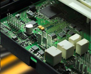
In closing, industrial control PCB is designed for automation equipment, industrial controllers, PLC modules, control panels, temperature control systems, and factory control electronics. This article explained how OEM buyers can confirm project requirements, use EBEST’s early DFM review, select the right PCB type, manufacture FR4 and multilayer PCB, add PCBA support, avoid manufacturing risks, and learn from an automation control panel case.

EBest Circuit (Best Technology) supports Industrial Control PCB projects with PCB fabrication, early DFM review, FR4 and multilayer production, HDI PCB, heavy copper PCB, metal base PCB, high-frequency PCB, industrial control PCB assembly, inspection, and customer-defined testing. For your next Industrial Control PCB project, please send your files and requirements to sales@bestpcbs.com.

You may also like

Robotics PCB Manufacturer

June 11th, 2026

Is your robotics PCB still stable after motor startup, sensor feedback and real motion testing? Many robotics PCB problems do not appear during basic power-on checks. They usually appear when the motor starts, the sensor begins sending feedback, or the robot runs under vibration and heat. At that stage, voltage drop, signal noise, AI module heating and weak connector soldering can delay the whole project.

EBest is a China source factory for robotics PCB manufacturing, PCB assembly, component sourcing and testing. Founded in 2006, EBest supports motion control PCB, sensor PCB, robot power PCB and AI module PCB from prototype to mass production, helping robot projects move from early validation to stable batch production.
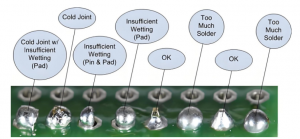
What Robotics PCB Problems Can EBest Help You Prevent?

EBest helps prevent unstable power, motor interference, sensor errors, AI module heating, solder joint failure and inconsistent batch quality before delivery. These issues often appear after basic power-on testing, especially when the robot starts moving under real motor load and vibration.
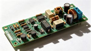
Common robotics PCB risks include:

  • Motor startup voltage drop that causes random reset
  • Sensor noise that affects detection and feedback
  • AI module heating that reduces long-term reliability
  • Weak connector soldering that fails under movement
  • Poor assembly consistency between prototype and batch production
  • Component sourcing delay before mass production
  • Insufficient testing before final delivery

A robotics PCB manufacturer should not only fabricate the board. It should review production risks, control soldering quality, check component availability and support testing before delivery.
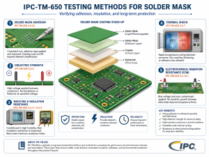
How Does EBest Support Robotics PCB Manufacturing?

EBest supports robotics PCB manufacturing through PCB design, PCB prototype, mass production, component sourcing, PCB assembly, inspection and testing. This keeps production review, parts preparation, assembly and delivery in one controlled process.

  • PCB design and production review
    EBest can review Gerber files, BOM, pick-and-place files and assembly drawings before production. This helps check power areas, component spacing, connector positions, test points and assembly risks before the robotics PCB enters fabrication.
  • PCB prototype for early robot testing
    Prototype service helps verify motion control, sensor feedback, robot power PCB stability and AI module function before batch production. Early sample testing can expose voltage drop, signal noise, heat issues or connector risks before the project moves forward.
  • Component sourcing for BOM control
    EBest reviews component availability, package type, lead time and sourcing risk before assembly. This is important for robotics PCB projects that use motor drivers, sensors, wireless modules, AI processors, connectors and high-current power components.
  • PCB assembly for robot applications
    EBest supports SMT assembly, THT assembly and mixed assembly for robotics PCB projects. This fits boards that combine compact ICs, sensors, connectors, terminals, motor driver circuits and power components on one PCBA.
  • Mass production for repeat orders
    After prototype validation, EBest can support small batch, mid-volume robotics PCB assembly and high-volume robotics PCB assembly. Controlled assembly and inspection help keep board quality more consistent across repeat orders.
  • Inspection and testing before delivery
    EBest can support AOI inspection, X-ray inspection, electrical testing, power-on testing and functional testing based on project requirements. For robot PCB assembly service, testing should confirm power, signal, communication and key module functions before shipment.

This service flow helps robotics PCB projects move from design files to assembled boards with clearer production control, fewer supplier handoffs and better preparation before batch delivery.

Which Robotics PCB Applications Can EBest Build?

EBest can manufacture and assemble robotics PCBs for motion control, motor drivers, sensor systems, power boards, AI modules, wireless communication and automation equipment. This allows one supplier to support several board types within the same robot project.

Typical robotics PCB applications include:

  • Motion control PCB
  • Motor driver PCB
  • Robot power PCB
  • Sensor control PCB
  • AI robot module PCB
  • AI robotics PCB manufacturing
  • Wireless communication PCB
  • Line follower robot PCB
  • Line following robot PCB
  • Inspection robot PCB
  • Industrial robot control PCB
  • Service robot PCB
  • Educational robot PCB

These boards often combine power, signal, communication and mechanical stress. As a result, PCB quality, component placement and inspection control directly affect robot operation.

Robotics PCB Applications

How Does PCB Quality Affect Robot Motion Accuracy?

PCB quality affects robot motion accuracy through power stability, motor driver performance, encoder signal quality, EMI control and assembly consistency. If the motor driver cannot receive stable current, the robot may move with delay, drift or random stop.

Motion control PCB projects usually include drivers, controllers, encoders, connectors and power circuits. When motor EMI affects encoder or control signals, the robot may move incorrectly even when the software logic is right.

For this reason, robotics PCB design should review power trace width, grounding, EMI separation, connector strength and test points before production. During assembly, accurate placement and strong solder joints help keep batch robots performing consistently.

Key review points include:

  • Motor control voltage: commonly 5V-48V
  • Control signal level: commonly 1.8V-5V
  • Encoder signal type: digital or analog
  • PCB copper weight: commonly 1oz-3oz
  • Test point spacing: commonly 1.0mm-2.54mm

How Do Sensor PCBs Improve Signal Stability in Robots?

Sensor PCBs improve signal stability by supporting clean grounding, low-noise routing, accurate component placement and reliable connector assembly. Stable sensor input helps robots detect objects, follow paths, avoid obstacles and control movement feedback.

In a line follower robot PCB, unstable sensor signals may cause the robot to drift, stop or misread the path. In inspection robots, poor signal quality may affect detection accuracy and response time.

Therefore, sensor PCB production should focus on grounding, connector quality, component polarity and signal integrity. EBest supports PCB in robotics applications where sensor stability must be checked together with assembly quality and testing requirements.

What Makes AI Robotics PCB Assembly More Challenging?

AI robotics PCB assembly is more challenging because AI modules often require stable power, thermal control, high-density SMT placement, camera interfaces and multi-sensor connections. The main risks are high current load, heat concentration, signal interference and hidden soldering defects.

AI robot power PCB projects may place processors, memory, wireless modules, sensors and power circuits in a compact area. If the assembly process is not controlled, BGA, QFN or small-pitch components may create hidden soldering defects.

AI robot testing PCB requirements should go beyond simple power-on checks. The test should confirm power stability, communication, sensor interface, camera connection and module operation before delivery to improve AI robot PCB reliability.

Robotics PCB Assembly

What Should Be Reviewed Before Robotics PCB Production?

Power layout, grounding, EMI control, thermal design, connector placement, component spacing, test points and BOM availability should be reviewed before robotics PCB production. This helps reduce rework before PCB fabrication and assembly begin.

A practical robotics PCB production review should check whether high-current areas are wide enough, whether sensor signals are protected from motor noise, and whether connectors can handle movement and vibration.

BOM review is also important. If key components are obsolete, out of stock or difficult to source, the project may face delay before batch assembly. EBest reviews these risks early so customers can adjust before production.

Production review should cover:

  • Power trace width for current capacity and heat control
  • Grounding design for signal and power return paths
  • EMI control for motor and switching noise reduction
  • Thermal layout for drivers, regulators and AI modules
  • Connector position for vibration-sensitive areas
  • Component spacing for SMT assembly clearance
  • Test point access for production testing
  • BOM availability for sourcing and lead time control

How Does PCB Assembly Quality Reduce Robotics PCB Failure Risk?

PCB assembly quality reduces robotics PCB failure risk by improving solder joint strength, connector reliability, component placement accuracy and inspection consistency. This is important for robot boards that work under movement, vibration, heat and repeated load changes.

Cold solder joints, insufficient solder, wrong polarity and shifted components may pass simple power-on checks. However, they can cause random failure during long-term robot operation or during system-level testing.

For robotics PCB assembly, SMT precision matters for ICs, sensors and communication modules. THT quality matters for terminals, connectors and power parts. Mixed assembly is useful when one robot board combines compact SMT devices with high-current components.

Assembly risk points include:

  • Cold solder joints that cause intermittent failure
  • Insufficient solder on high-current pads
  • Wrong polarity components that damage power circuits
  • Connector solder cracks under vibration
  • Shifted components that affect signal or power paths
  • Flux residue that may affect long-term reliability
  • Batch inconsistency between prototype and repeat orders

What Tests Are Needed Before Robotics PCB Delivery?

AOI, X-ray inspection, electrical testing, functional testing, power-on testing, thermal review and customized reliability testing may be required before robotics PCB delivery. The final test plan should match the robot’s working environment and board function.

Common robotics PCB tests include:

  • AOI inspection for SMT placement and soldering quality
  • X-ray inspection for BGA, QFN and hidden solder joints
  • Electrical test for open and short circuit checking
  • Functional test for power, signal and communication
  • Power-on test for basic operating confirmation
  • Thermal review for motor drivers, regulators and AI modules
  • Connector inspection for vibration-sensitive applications
  • Custom robot PCB reliability test based on project requirements

These tests help reduce delivery risk before the robot enters full system testing. For AI robot testing PCB projects, power, signal and communication checks should be confirmed before shipment.

Case Study: Reducing Motion and Sensor Issues Before Batch Production

A robotics PCB project can pass basic power-on testing but still fail during real movement if motor load, sensor noise, vibration and soldering quality are not controlled before batch production. This case shows how production review helps reduce motion and sensor risks before mid-volume assembly.

Project Background

The customer was developing a mobile robot control board for motor control, sensor feedback and power distribution. The prototype could power on, but the board reset when the motor started. During movement testing, the sensor signal also became unstable, which affected motion accuracy and feedback reliability.

Customer Requirements

The project required stable power delivery, lower motor interference, stronger connector soldering, cleaner sensor feedback and consistent PCB assembly quality. The customer also wanted to reduce repeated prototype rework before moving to batch production.

Our Solution

EBest reviewed the Gerber files, BOM, assembly drawing and testing requirements before production. Our team checked high-current power areas, grounding paths, connector positions, component sourcing risks and assembly feasibility. During production, EBest controlled SMT placement, THT soldering, connector assembly, inspection and functional testing.

Output Result

The project moved from prototype validation to mid-volume robotics PCB assembly with lower production risk. The board showed lower reset risk during motor startup, more stable sensor feedback during movement and better consistency before robot system-level testing.

Key results included:

  • Lower motion failure risk during motor startup
  • More stable sensor feedback during robot movement
  • Stronger connector soldering for vibration-sensitive areas
  • Better batch consistency before mid-volume production
  • Less rework before final robot system testing
  • Faster transition from prototype validation to batch assembly

Why Choose EBest for Robotics PCB Manufacturing?

EBest provides PCB fabrication, component sourcing, PCB assembly, testing support and batch production service from one China source factory. For robotics PCB projects, this helps reduce supplier handoff, shorten communication time and lower production risk before delivery.

  • One-stop PCB and PCBA service
    EBest supports PCB design, PCB prototype, mass production, component sourcing and PCB assembly in one service flow. This keeps board production, parts sourcing and assembly communication in the same production chain.
  • 20+ years of PCB manufacturing experience
    Founded on June 28, 2006, EBest Circuit, also known as Best Technology, has over 20 years of PCB manufacturing experience. This supports robotics PCB production review from prototype verification to stable batch production.
  • Monthly production capability
    EBest’s monthly production capability reaches 260,000 square feet / 28,900 square meters, with more than 1,000 different boards completed monthly. This capacity supports prototype runs, repeat orders, mid-volume robotics PCB assembly and high-volume robotics PCB assembly.
  • Expedited service for urgent boards
    For urgent boards, EBest can provide expedited service, and eligible urgent boards can be shipped within 24 hours when project files, materials and production conditions allow. This is suitable for robotics PCB prototype verification and pilot production schedules.
  • Wide robotics PCB structure support
    EBest supports FR4 PCB, multi-layer PCB, Metal Core PCB, Ceramic PCB, flexible PCB, rigid-flex PCB, RF PCB, High Tg PCB, heavy copper PCB, HDI PCB, high-speed PCB, impedance control PCB and busbar PCB. These options fit robot power PCB, sensor PCB, motion control PCB and AI module PCB requirements.
  • SMT, THT and mixed assembly capability
    EBest supports SMT assembly, THT assembly and mixed assembly for robotics PCB projects. This is important for boards that combine compact ICs, sensors, connectors, terminals and high-current power components.
  • Certified quality and compliance systems
    EBest holds IATF 16949, ISO 9001:2015, ISO 13485:2016, AS9100D, REACH, RoHS and UL. These certifications support process control, material compliance and quality management for global B2B applications.
  • China source factory with global delivery
    EBest does not claim overseas factories, overseas warehouses or local branches. The service is based on China source-factory manufacturing, component sourcing, PCB assembly and global delivery support.

For robotics PCB assembly, EBest supports motion accuracy, sensor stability, AI robot PCB reliability and batch delivery through controlled manufacturing, assembly and testing.

Robotics PCB

What Files Should You Send for a Robotics PCB Quote?

Send Gerber files, BOM, pick-and-place file, assembly drawing, quantity, testing requirements and special notes about motor load, vibration, heat or working environment for a robotics PCB quote. Complete files help EBest review cost, lead time and production feasibility faster.

Recommended quote files include:

  • Gerber file in RS-274X format
  • BOM in XLS, XLSX or CSV format
  • Pick-and-place file in CSV or TXT format
  • Assembly drawing in PDF format
  • PCB stack-up if required
  • Surface finish requirement
  • Order quantity in units or panels
  • Testing requirement in PDF or TXT format
  • Special notes for motor load, vibration, heat or working environment

If the project includes AI modules, high-current motor drivers or critical sensors, share the test method and operating condition early. This allows a more accurate production review and reduces repeated confirmation before quotation.

FAQs About Robotics PCB Manufacturing

Q1: What is the MOQ for robotics PCB assembly?
A1: The MOQ depends on PCB complexity, component sourcing and testing requirements. For prototype projects, EBest can support small trial orders. For repeat production, mid-volume or high-volume robotics PCB assembly is more suitable after the design, BOM and test process are stable.

Q2: Can EBest source components for robotics PCB assembly?
A2: Yes. EBest can support component sourcing based on the customer’s BOM. Before assembly, the team can review part numbers, package types, availability and lead time risks. For motor drivers, sensors, connectors and AI modules, early BOM review helps reduce production delay.

Q3: What affects the cost of a robotics PCB project?
A3: The main cost factors include PCB layer count, board size, copper weight, surface finish, component quantity, package difficulty, assembly type, testing scope and order volume. BGA, QFN, fine-pitch parts, high-current areas and functional testing can increase the total project cost.

Q4: Should I send a test fixture for robotics PCB functional testing?
A4: If the board requires motion control, sensor feedback, communication or AI module verification, a test fixture is recommended. A fixture helps confirm power, signal and interface functions more consistently before shipment, especially for batch robotics PCB assembly and repeat orders.

Q5: Can EBest handle alternative components if some parts are out of stock?
A5: EBest can help review possible alternative components, but final approval should come from the customer. For robotics PCB projects, replacement parts must match package size, electrical rating, tolerance, temperature range and functional requirements before they are used in production.

Q6: What files are required for faster robotics PCB quotation?
A6: For faster quotation, send Gerber files, BOM, pick-and-place file, assembly drawing, quantity and testing requirements. If the robotics PCB includes motor drivers, sensors, AI modules or high-current circuits, include operating conditions and special inspection notes early.

Q7: Can EBest support both prototype and batch robotics PCB production?
A7: Yes. EBest supports PCB prototype, small batch, mid-volume and high-volume robotics PCB assembly. Prototype production is used for function verification, while batch production focuses on assembly repeatability, inspection control, component supply and delivery consistency.

Q8: What should be confirmed before moving from prototype to batch production?
A8: Before batch production, confirm circuit function, BOM stability, test method, component availability, connector strength, thermal performance and assembly process. For robotics PCB projects, motor load, sensor stability and AI module power behavior should be checked before scaling.

Q9: Can EBest assemble robotics PCBs with both SMT and THT parts?
A9: Yes. EBest supports SMT, THT and mixed assembly. This is useful for robotics PCB projects that combine small ICs, sensors, wireless modules, connectors, terminals and high-current power components on the same board.

Q10: What surface finish is suitable for robotics PCB manufacturing?
A10: Common surface finishes include HASL, lead-free HASL, ENIG and OSP. The right choice depends on component package, soldering requirement, shelf life, cost and reliability needs. For fine-pitch components, BGA or AI module boards, ENIG is often considered during production review.

Q11: How can robotics PCB batch consistency be improved?
A11: Batch consistency can be improved through stable BOM control, clear assembly drawings, approved process settings, AOI inspection, soldering control, functional testing and consistent packaging. For robotics PCB assembly, repeatable production control is important because small defects may affect robot movement or sensor feedback.

Q12: Can EBest support urgent robotics PCB prototype orders?
A12: EBest can provide expedited service for urgent boards when project files, materials and production conditions allow. Eligible urgent boards can be shipped within 24 hours. For faster handling, customers should provide Gerber files, BOM, quantity and assembly requirements at the beginning.

Q13: What certifications does EBest have for PCB manufacturing?
A13: EBest holds IATF 16949, ISO 9001:2015, ISO 13485:2016, AS9100D, REACH, RoHS and UL. These systems support process control, quality management and compliance needs for global B2B PCB projects, including robotics PCB manufacturing and assembly.

Q14: Can a China source factory support overseas robotics PCB projects?
A14: Yes. A China source factory can support overseas robotics PCB projects through custom manufacturing, component sourcing, PCB assembly, testing and global delivery. EBest does not claim overseas factories, overseas warehouses or local branches. The service is based on China source-factory production.

Get a Robotics PCB Quote for Your Project

A reliable robotics PCB should support stable motion, clean sensor feedback, controlled power delivery and tested assembly quality before it enters real robot operation. For motion control boards, sensor boards, AI robot modules and robot power PCB projects, early production review can reduce rework, prevent batch inconsistency and lower delivery risk.

For selection, choose a robotics PCB manufacturer that can review design files, source components, assemble SMT and THT parts, inspect solder quality and support functional testing. For procurement, prepare complete Gerber files, BOM, pick-and-place files, quantity and test requirements before requesting a quote.

EBest Circuit is a China source factory supporting robotics PCB manufacturing and assembly, component sourcing, testing and global delivery for robot projects. Send your Gerber files, BOM, quantity and testing requirements to sales@bestpcbs.com for a robotics PCB manufacturing and assembly quote.

You may also like

New Energy PCB Manufacturer with One-Stop PCB and PCBA Support

June 11th, 2026

New Energy PCB is used in EVs, chargers, energy storage systems, solar inverters, LED power modules, and power control electronics. This article explains how EBest Circuit (Best Technology) supports New Energy PCB projects with PCB fabrication, material review, PCBA assembly, testing, and engineering communication.

What problems do OEM buyers often face in New Energy PCB projects?

  • Wrong material choice: FR4, high-Tg FR4, aluminum, copper base, ceramic, HDI, or heavy copper may all be possible.
  • Slow prototype review: Missing stack-up, copper thickness, or test notes can delay quotation.
  • Unclear current and heat requirements: High-current areas may need thicker copper or better thermal paths.
  • PCBA handoff risk: PCB, BOM, SMT, DIP, and testing may be handled by separate suppliers.
  • Low-price trap: A cheap quote may ignore manufacturability, testing, or repeat production.

EBEST helps reduce these risks with focused engineering review.

  • Material matching: We review board type, copper thickness, Tg, and thermal needs.
  • Fast file review: We check Gerber files, stack-up, BOM, and assembly drawings early.
  • High-current support: We review copper weight, terminals, connectors, and heat paths.
  • One-stop PCBA: We connect PCB fabrication, sourcing review, SMT, DIP, inspection, and testing.
  • Repeatable production: We review prototype projects with later small-batch and repeat orders in mind.

EBest Circuit (Best Technology) is a PCB and PCBA manufacturer supporting FR4 PCB, high-Tg FR4 PCB, heavy copper PCB, aluminum PCB, copper base PCB, ceramic PCB, HDI PCB, rigid-flex PCB, RF microwave high-frequency PCB, and PCBA assembly. For New Energy PCB projects, please send Gerber files, BOM, stack-up, copper thickness, material notes, assembly drawings, testing requirements, quantity, and delivery target to sales@bestpcbs.com.

New Energy PCB

What Should OEM Buyers Confirm Before Starting a New Energy PCB Project?

Before starting a New Energy PCB project, OEM buyers should confirm the real operating conditions. These details decide the material, copper thickness, thermal structure, assembly method, and testing plan.

ItemWhat to Confirm
ApplicationEV, charger, energy storage, inverter, LED, or power control
Current loadSignal board, power board, or high-current path
Thermal needStandard FR4, aluminum, copper base, ceramic, or other option
PCBA scopeBare PCB only or PCB plus assembly
Testing needElectrical test, functional test, aging, or customer test method

EBEST does not use one PCB type for every new energy project. We review the application first, then match the board structure.

For example, a control board may use high-Tg FR4. A heat-focused board may need aluminum or copper base. A high-current board may need heavy copper. A compact control module may need HDI. A high-power thermal design may need ceramic PCB.

A clear project start helps reduce quotation changes and production delay.

How Can EBEST Speed Up New Energy PCB Prototype Review?

A New Energy PCB prototype should help customers test faster, not create new questions during production. EBEST speeds up prototype review by checking the key files before fabrication.

We usually review:

  • Gerber and drill files
  • Stack-up
  • Board thickness
  • Copper thickness
  • Material grade
  • Surface finish
  • Minimum line width and spacing
  • Minimum hole size
  • High-current areas
  • Connector and terminal zones
  • Test points
  • BOM and assembly drawings if PCBA is needed

For high-Tg FR4 projects, EBEST can review Tg requirements such as standard Tg, Tg 150, or Tg 170–180 options. For high-frequency or communication-related new energy boards, we can review materials such as Rogers, Taconic, Arlon, Nelco, and other specified laminates when required.

For prototype projects, the goal is simple: confirm what can be built, what may affect lead time, and what should be adjusted before mass production.

What Does EBEST Check Before Quoting a New Energy Vehicle PCB?

Before quoting a New Energy Vehicle PCB, EBEST reviews cost-driving and risk-driving details. A useful quote should reflect the real board, not only the size and quantity.

We check:

  • Layer count
  • Board thickness
  • Copper weight
  • Material type
  • Surface finish
  • HDI or blind/buried via structure
  • Heavy copper requirement
  • Impedance requirement
  • Connector and terminal areas
  • Minimum hole size
  • Solder mask bridge
  • Electrical testing
  • PCBA and functional testing needs

EBEST’s process capability covers a wide range of PCB requirements, including multilayer PCB, HDI PCB, heavy copper PCB, aluminum PCB, high-frequency PCB, and thick board projects. For heavy copper designs, line width and spacing must be reviewed together with copper weight. For example, a 1 oz board and a 10 oz or 20 oz heavy copper board cannot use the same fabrication rules.

That is why New Energy Vehicle PCB quotation must start with engineering review.

A low quote without copper, material, and testing review is not a reliable quote.

How Does EBEST Support New Energy Charger PCB Assembly?

New Energy Charger PCB Assembly usually involves power components, connectors, relays, transformers, terminals, heat-generating parts, and test requirements. EBEST reviews the PCB and PCBA together so the project does not fail at the assembly stage.

Our support can include:

  • PCB fabrication
  • BOM review
  • Component sourcing review
  • SMT assembly
  • DIP assembly
  • BGA/QFN assembly when needed
  • Connector and terminal assembly
  • AOI inspection
  • X-ray inspection when required
  • First article inspection
  • Customer-defined functional testing

For charger boards, we focus on high-current paths, spacing, soldering areas, connector strength, thermal zones, and test access. If the PCB design is difficult to assemble, we will raise the issue before production.

This is the value of one-stop PCB and PCBA support: fewer handoffs, clearer responsibility, and better preparation for repeat orders.

Which PCB Technologies Can EBEST Match to New Energy Applications?

New Energy PCB is not one fixed board type. EBEST matches PCB technology based on current, heat, space, reliability, and assembly needs.

PCB TechnologySuitable New Energy Use
FR4 PCBControl boards and signal circuits
High-Tg FR4 PCBHigher thermal resistance
Heavy Copper PCBHigh-current paths and power distribution
Aluminum PCBLED power and heat dissipation
Copper Base PCBHigh thermal transfer power boards
Ceramic PCBHigh-power and high-thermal applications
HDI PCBCompact control modules
High-Frequency PCBCommunication or RF-related modules
Rigid-Flex PCBSpace-limited or vibration-sensitive products

EBEST also supports multiple surface finishes, including HASL, lead-free HASL, ENIG, immersion tin, immersion silver, hard gold, soft gold, ENEPIG, carbon ink, and gold finger plating when required.

This matters because new energy products may need more than standard FR4. A charger, inverter, EV control board, battery system, or LED power board may need different copper, material, surface finish, and assembly plans.

The right PCB technology should support the product, not just meet the drawing.

What Manufacturing Challenges Should New Energy PCB Buyers Watch For?

New Energy PCB projects often fail because small manufacturing details are ignored early.

Common risks include:

  • Copper mismatch
    High-current areas may need thicker copper or wider current paths.
  • Wrong material
    Standard FR4 may not be enough for thermal or reliability needs.
  • Poor thermal path
    Heat may require aluminum, copper base, ceramic, or better copper design.
  • Connector stress
    Terminals, screws, and power connectors may create mechanical risk.
  • Unclear testing
    Electrical test alone may not prove product function.

EBEST reduces these risks through DFM review, material confirmation, process capability review, PCBA planning, inspection, and customer-defined testing.

For new energy projects, “cheap” should not be the main decision. A practical supplier should help control cost while protecting manufacturability and reliability.

The better result is a board that can be built, assembled, tested, and repeated.

New Energy Charger PCB Assembly Case: How Did EBEST Support an OEM Customer?

An OEM customer needed a New Energy Charger PCB Assembly project for a power control board used inside new energy charging equipment. The board had to support power-control signals, connector interfaces, stable impedance performance, and reliable PCBA assembly for later repeat production.

For this project, EBEST focused on five key areas:

  • Application review
    The PCB was used in a new energy charger power control module, so EBEST reviewed the design around signal stability, connector layout, assembly reliability, and production repeatability.
  • Complex PCB structure
    This was a 12-layer FR4 PCB with Tg 170 material, 1 oz inner and outer copper, 4.8 mm board thickness, ENEPIG surface finish, and controlled impedance requirements.
  • Engineering review before production
    EBEST reviewed the Gerber files, BOM, stack-up, copper thickness, impedance notes, assembly drawing, and testing requirements before fabrication and assembly.
  • Manufacturing and assembly control
    The review focused on multilayer stack-up, ENEPIG process control, impedance control, connector reliability, soldering process stability, AOI inspection, first article checking, and customer-defined test support.
  • One-stop project value
    EBEST helped the customer reduce communication gaps between PCB fabrication, BOM review, SMT assembly, DIP connector assembly, inspection, and testing.

Key project parameters:

  • Application: New energy charger power control board
  • PCB type: 12-layer FR4 PCB
  • Material Tg: Tg 170
  • Copper thickness: 1 oz inner and outer copper
  • Board thickness: 4.8 mm ±10%
  • Solder mask / silkscreen: Green solder mask, white silkscreen
  • Surface finish: ENEPIG
  • Nickel thickness: 120 μin–276 μin
  • Palladium thickness: 1 μin–5 μin
  • Gold thickness: 1 μin
  • Impedance: Controlled impedance required
  • PCBA scope: SMT assembly, DIP connector assembly, inspection, and customer-defined test support
  • Project value: PCB fabrication and PCBA assembly were reviewed together to improve manufacturability and repeat production stability.
New Energy PCB

FAQs About New Energy PCB

What Is a New Energy PCB?
A New Energy PCB is a printed circuit board used in EVs, chargers, solar systems, energy storage, inverters, power electronics, LED systems, and related control modules.

Can EBEST Support New Energy PCB Prototype Projects?
Yes. EBEST can review Gerber files, stack-up, copper thickness, material choice, surface finish, BOM, assembly drawings, and test requirements before production.

What PCB Types Are Common in New Energy Projects?
Common options include FR4 PCB, high-Tg FR4 PCB, heavy copper PCB, aluminum PCB, copper base PCB, ceramic PCB, HDI PCB, high-frequency PCB, and rigid-flex PCB.

Can EBEST Provide New Energy Charger PCB Assembly?
Yes. EBEST can support PCB fabrication, component sourcing review, SMT assembly, DIP assembly, inspection, and customer-defined testing for charger PCB projects.

What Files Should I Send for a New Energy PCB Quote?
Please send Gerber files, drill files, stack-up, copper thickness, material notes, BOM, pick-and-place file, assembly drawing, testing requirements, quantity, and delivery target.

All in all, new energy PCB supports EVs, chargers, energy storage, solar systems, inverters, LED power, and other power electronics products. This article explained how EBEST reviews material, copper, prototype files, charger PCBA needs, PCB technologies, manufacturing risks, and one real charger PCBA case.

EBest Circuit (Best Technology) supports New Energy PCB projects with PCB fabrication, PCBA assembly, material review, component sourcing review, SMT, DIP, inspection, testing, and engineering communication. Please send your files and requirements to sales@bestpcbs.com for review.

You may also like

Custom IoT Circuit Board Manufacturer for Wearables and Detectors

June 10th, 2026

Is your IoT circuit board reliable enough for stable wireless performance, compact assembly and long-term product use? Many connected devices are small on the outside, but the internal circuit board must handle sensors, wireless modules, power control, programming interfaces and enclosure restrictions at the same time.

A well-built IoT circuit board helps improve signal stability, assembly quality and production consistency. For wearables, detectors, tracking devices and smart terminals, the right board structure, material selection, RF layout and assembly control can directly affect product reliability.

 IoT Circuit Board

What Is an IoT Circuit Board and Why Is It Important for Smart Devices?

An IoT circuit board is the electronic platform that connects sensors, processors, wireless modules, power circuits and communication interfaces inside a connected device. It allows the product to collect data, process signals and send information through Wi-Fi, Bluetooth, NB-IoT, LTE-M, LoRa, Zigbee or other wireless technologies.

For smart devices, the board does much more than hold components. It affects wireless stability, battery performance, sensor accuracy, heat control, product size and assembly yield. If the PCB layout, material, soldering or testing is not controlled properly, the final device may show weak signals, unstable operation or early failure.

This is especially important for wearables and detectors because internal space is limited. A reliable IoT circuit board must support compact routing, stable grounding, clean power delivery, accurate sensor placement and proper antenna clearance.

What Types of IoT Circuit Boards Are Used in Wearables, Detectors and Smart Devices?

Different IoT products require different circuit board structures. The selection depends on product size, bending space, wireless function, assembly method and expected working environment.

PCB TypeCommon UseMain Advantage
Rigid PCBDetectors, controllers, gatewaysStable structure and mature production
Flexible PCBWearables, smart bands, compact sensorsThin, lightweight and bendable
Rigid-flex PCBMedical wearables, AI devices, compact modulesReduces connectors and saves space
HDI PCBSmall IoT modules and high-density devicesSupports fine routing and compact layout
Metal-core PCBLighting IoT and heat-sensitive devicesImproves thermal control
Multilayer PCBIndustrial IoT and wireless terminalsSupports power, signal and ground separation

IoT flexible circuit boards are common in wearable devices because they can fit curved spaces and moving structures. However, flexible PCB projects must confirm bend radius, copper thickness, stiffener location, connector reinforcement and coverlay opening before production.

Rigid-flex PCB is also popular in compact IoT devices. It can reduce cable connections, improve internal reliability and make assembly cleaner. For small smart products, this structure can make the whole device easier to assemble and more stable during repeated use.

Where Are IoT Circuit Boards Commonly Used?

IoT circuit boards are used in connected products that collect, process and transmit data. These products often combine sensors, wireless modules, batteries, displays, buttons, alarms or cloud communication functions.

Common applications include:

  • IoT wearable circuit board for smart watches, wristbands, health monitors and portable AI devices
  • IoT detector circuit board for smoke detection, gas detection, motion detection and environmental monitoring
  • Smart home sensors for temperature, humidity, light, door status and water leakage
  • Industrial IoT modules for equipment monitoring, remote control and predictive maintenance
  • Asset tracking devices using GPS, BLE, NB-IoT, LTE-M or LoRa communication
  • Smart agriculture sensors for soil, moisture, weather and irrigation control
  • Healthcare monitoring devices with compact sensing and wireless transmission
  • Access control terminals, wireless alarms and smart security devices

In these applications, the IoT circuit board must support stable wireless communication, accurate signal capture and reliable assembly. A small layout issue can affect connection range, sensing accuracy or long-term operation.

What Challenges Occur When Designing Printed Circuit Boards in IoT?

Designing printed circuit boards in IoT is challenging because wireless performance, sensor accuracy, power management and product size often compete for limited space. A board may pass basic testing on a workbench but perform poorly after being installed inside the final enclosure.

Common challenges include:

  • Poor antenna clearance causing weak wireless range
  • Noisy power circuits affecting sensors, RF modules or MCU stability
  • Battery placement blocking antenna radiation or increasing local heat
  • Grounding mistakes causing interference and unstable signals
  • Dense routing creating crosstalk or assembly difficulty
  • Connector stress in wearable and portable devices
  • Insufficient test points slowing programming and inspection
  • Wrong flexible area design causing copper cracks after bending

In IoT products, the PCB, antenna, battery, enclosure and firmware interface should be reviewed together. A board that works in open-air testing may behave differently inside a plastic shell, metal frame or wearable housing.

How to Design an IoT Circuit Board for Stable Wireless Performance?

A stable IoT circuit board starts with proper RF planning, clean power delivery and careful component placement. Wireless performance should be considered before routing, enclosure design and assembly confirmation.

  • Plan the antenna area first
    Keep the antenna away from batteries, metal parts, shields, connectors and dense copper areas. Reserve enough keep-out space around the antenna and avoid placing large components near the antenna radiation area.
  • Control the RF trace
    Keep RF traces short, direct and smooth. Use controlled impedance when required by the wireless module, and avoid unnecessary vias, sharp corners, long stubs and sudden width changes.
  • Place RF matching components correctly
    Place RF matching components close to the antenna feed point. Leave enough space for tuning components so wireless performance can be adjusted after sample testing.
  • Build a clean grounding structure
    Use a continuous ground reference under sensitive signal areas. Avoid broken ground planes near RF traces and keep the antenna clearance area free from copper when required by the antenna type.
  • Separate power, RF and sensor areas
    Place switching power circuits away from antennas and RF modules. Keep high-current traces away from wireless and sensor signals to reduce interference.
  • Use proper decoupling capacitors
    Place decoupling capacitors close to IC power pins. This helps reduce voltage ripple and improves the stability of MCUs, sensors and wireless modules.
  • Review wireless module placement
    Follow the module supplier’s layout recommendation. Keep module antennas near the board edge when required and avoid placing them under displays, batteries or metal covers.
  • Consider enclosure impact
    Check whether the housing is plastic, metal or mixed material. Avoid placing antennas too close to screws, brackets, metal frames or battery packs.
  • Prepare for RF testing
    Add test points for power, ground and communication interfaces. Test wireless range, signal strength and connection stability under real product conditions.
  • Validate with final assembly
    Test the IoT circuit board with the real enclosure, battery, cable and installation method. Final wireless performance should not rely only on open-bench testing.
 IoT Circuit Board Design

What Should Be Confirmed Before Manufacturing Printed Circuit Boards in IoT?

Before manufacturing printed circuit boards in IoT, the production files and technical requirements should be checked carefully. This reduces file misunderstanding, incorrect material selection, assembly delay and repeated revisions.

Confirm the following items before production:

  • Gerber files and drill files
  • BOM with exact part numbers and package information
  • PCB stack-up, material and copper thickness
  • Board thickness and surface finish
  • Impedance control requirements
  • Antenna clearance and RF routing notes
  • Panelization method and breakaway structure
  • Flexible PCB bend radius and stiffener position
  • Test points for power, programming and function checking
  • Assembly drawings and polarity markings
  • Firmware flashing method if required
  • Final functional test requirements before shipment

This confirmation is very important for compact smart devices. Wearables, detectors and wireless modules usually have tight internal space, so even small changes in board thickness, connector position or antenna area may affect final assembly.

What Are the Manufacturing Processes for IoT Circuit Boards?

The manufacturing process for an IoT circuit board should control material, copper quality, hole plating, solder mask accuracy, surface finish and final inspection. Each step affects assembly accuracy and product reliability.

1. Production file review
Check Gerber files, drill files, stack-up, copper thickness and board outline. Confirm impedance control, minimum trace width, spacing, hole size, solder mask clearance, panelization and special RF notes.

2. Material preparation
Select PCB material according to board structure and application. Confirm FR4, high-Tg FR4, flexible polyimide or other required materials, as well as copper thickness and laminate thickness.

3. Inner layer imaging and etching
Transfer circuit patterns onto inner copper layers, etch unwanted copper and inspect inner circuits for opens, shorts and pattern defects.

4. Lamination
Stack inner layers, prepreg and copper foil according to the approved stack-up. Press layers under controlled temperature, pressure and time to ensure stable bonding.

5. Drilling
Drill through holes, vias, mounting holes and slots. Control hole position accuracy and clean drilled holes before plating.

6. Copper plating
Plate copper inside drilled holes to build conductive connections between layers. Control plating thickness and inspect for voids, thin copper and poor hole-wall quality.

7. Outer layer imaging and etching
Transfer outer circuit patterns, plate and etch outer copper layers. Check fine traces, pads, RF routes and connector areas.

8. Solder mask application
Apply solder mask to protect copper and prevent solder bridging. Control solder mask openings for fine-pitch pads, test points and RF areas.

9. Surface finish
Apply the required surface finish according to assembly requirements. Common options include ENIG, lead-free HASL, OSP, immersion silver and immersion tin.

10. Profiling and panel routing
Route board outlines, slots, cutouts and special shapes. Add V-cut or tab routing when required and confirm edge quality.

11. Electrical testing
Test for open circuits, short circuits and netlist consistency. Verify connectivity between layers and inspect high-risk fine-pitch or via areas.

12. Final inspection and packing
Inspect appearance, solder mask, surface finish, dimensions, warpage, scratches and exposed copper. Pack boards with moisture and handling protection.

For IoT flexible circuit boards, additional attention should be placed on polyimide material, coverlay alignment, stiffener bonding and bend-zone quality. These details help reduce cracking, delamination and connector failure during product use.

IoT Circuit Board Manufacturing Process

How Does IoT Circuit Board Assembly Affect Product Reliability?

IoT circuit board assembly has a direct impact on final product reliability. Many IoT devices use fine-pitch ICs, compact sensors, wireless modules, small connectors, batteries and antennas, so assembly accuracy is very important.

Important assembly controls include:

  • Accurate solder paste printing for fine-pitch components
  • Stable SMT placement for sensors, MCUs and wireless modules
  • Controlled reflow profile to reduce solder voids and weak joints
  • AOI inspection for polarity, offset, bridging and missing parts
  • X-ray inspection for BGA, QFN and hidden solder joints when required
  • Programming and functional testing before shipment
  • Connector strength review for wearable and portable products
  • Clean handling for sensors, RF areas and exposed contacts

For wearable products, the assembly process should also consider button position, battery connection, enclosure fit and charging interface alignment. For detector products, sensor direction, alarm output, wireless communication and power stability should be checked before delivery.

A reliable assembly process helps reduce field failure, restart problems, unstable signals and sensor response errors. This is why IoT circuit board manufacturing and assembly should be reviewed as one complete production flow.

How to Test an IoT Circuit Board Before Mass Production?

An IoT circuit board should be tested for power stability, wireless performance, sensor response, assembly quality and real-use reliability before mass production. Testing should cover both the bare PCB and the assembled board.

  • Check bare PCB quality
    Test for opens and shorts. Check board outline, holes, slots, connector positions, solder mask quality, surface finish, scratches, exposed copper and board warpage.
  • Verify power circuits
    Check input voltage range, output voltage, current consumption, sleep current and standby current. For battery-powered devices, check charging circuits and battery protection.
  • Test programming and boot function
    Confirm firmware flashing, MCU boot process, reset circuit, clock signal, memory communication and programming success rate.
  • Test wireless communication
    Check Wi-Fi, Bluetooth, NB-IoT, LTE-M, LoRa, Zigbee or other wireless functions. Measure signal strength, connection stability, reconnection ability and wireless range.
  • Test sensor performance
    Check sensor response speed, data accuracy, calibration process and signal stability. Test sensor performance after the board is installed inside the final enclosure.
  • Inspect soldering quality
    Use AOI to check missing parts, polarity errors, offset and solder bridging. Use X-ray for BGA, QFN, LGA and hidden solder joints when required.
  • Run functional testing
    Check buttons, LEDs, buzzers, relays, displays, charging ports, communication ports and alarm output. Confirm all product functions against the test plan.
  • Run reliability checks
    Perform power cycling, long-time operation, thermal behavior checks, connector plug-in tests and basic vibration, drop or bending checks when required.
  • Test with final assembly condition
    Install the PCB inside the real enclosure. Add the final battery, cables, buttons and display, then check mechanical fit, antenna performance and heat behavior.
  • Approve before production
    Review all test results, correct sample issues, freeze Gerber files, BOM and test procedures, then move to mass production after stable validation.
IoT Circuit Board Test

How to Choose a Reliable IoT Circuit Board Manufacturer?

Choosing a reliable IoT circuit board manufacturer should focus on production capability, assembly control, testing support and communication quality. A good manufacturer should help reduce production risk before the board enters batch production.

  • Check IoT production experience
    Choose a manufacturer with experience in wireless modules, sensors, batteries, compact devices, wearables and detectors.
  • Confirm PCB manufacturing capability
    Make sure the manufacturer can support rigid PCB, flexible PCB, rigid-flex PCB, HDI PCB and multilayer PCB when required.
  • Review assembly capability
    Check whether they can handle SMT assembly, fine-pitch ICs, QFN, BGA, sensors, connectors, shields and wireless modules.
  • Ask about RF and antenna awareness
    A reliable supplier should understand antenna clearance, RF trace control, grounding and enclosure impact on wireless performance.
  • Check material and surface finish options
    Confirm support for FR4, high-Tg FR4, polyimide, ENIG, lead-free HASL, OSP and other suitable options.
  • Confirm inspection methods
    Look for electrical testing, AOI inspection, X-ray inspection, visual inspection and dimensional checking.
  • Check functional testing support
    For IoT products, the manufacturer should support power testing, programming, wireless testing, sensor testing and final function checking.
  • Review file checking ability
    The manufacturer should check Gerber files, BOM, stack-up, polarity markings, test points and panelization before production.
  • Confirm batch consistency
    Ask how they control repeat orders, material traceability, soldering quality and production records.
  • Evaluate communication quality
    Choose a manufacturer that gives clear feedback, confirms production details and points out risks before manufacturing.
  • Check customization support
    A strong manufacturer should support custom board size, stack-up, material, assembly process and testing requirements.
  • Choose one-stop support when possible
    For IoT circuit board projects, PCB fabrication, component sourcing, SMT assembly and testing under one supplier can reduce coordination risk.

Why Choose EBest as Your IoT Circuit Board Manufacturer?

As an IoT circuit board manufacturer, EBest provides custom IoT PCB manufacturing and assembly support for wearables, detectors, smart sensors and wireless devices. We help turn your PCB files into reliable finished boards through manufacturing review, PCB fabrication, SMT assembly and testing support.

  • Custom PCB support
    EBest can support rigid PCB, flexible PCB, rigid-flex PCB, HDI PCB and multilayer PCB for different IoT products.
  • One-stop production service
    We can support PCB fabrication, component sourcing, SMT assembly, inspection and functional testing in one process.
  • Better risk control before production
    We can review Gerber files, BOM, stack-up, assembly drawings and test requirements before manufacturing starts.
  • Support for compact IoT devices
    We can handle fine-pitch components, sensors, connectors, batteries, wireless modules and small board layouts.
  • Reliable quality inspection
    EBest can provide electrical testing, AOI inspection, visual inspection, dimensional checking and functional testing based on project requirements.
  • Support from prototype to repeat production
    We can help with sample builds, production adjustment and stable batch manufacturing for long-term IoT projects.

With EBest, you get more than PCB production. You get practical manufacturing support, assembly control and quality inspection to help your IoT circuit board project move forward with less production risk.

FAQs About IoT Circuit Board

Q1: What information helps speed up an IoT circuit board project review?
A1: Complete Gerber files, BOM, PCB specifications, assembly drawings, polarity notes, test requirements and enclosure information help speed up project review. If wireless performance is important, antenna position and module details should also be included.

Q2: Can the same IoT circuit board be used for prototype and batch production?
A2: Yes, but the prototype version should be reviewed before batch production. Component availability, panelization, test points, soldering quality and enclosure fit should be confirmed before repeat orders.

Q3: What should be checked if an IoT device has unstable battery life?
A3: The main points include sleep current, standby current, regulator efficiency, wireless transmission time, sensor working cycle and charging circuit behavior. Battery life problems are often related to both circuit design and firmware settings.

Q4: How can component shortages affect an IoT circuit board order?
A4: Component shortages may delay assembly or require approved alternatives. For smoother production, the BOM should include exact part numbers, package details and acceptable substitute options when available.

Q5: What is important for wearable IoT circuit board reliability?
A5: Wearable products require attention to board thickness, flexible area bending, connector strength, battery connection, charging contacts, sweat resistance, enclosure pressure and long-term mechanical stress.

Q6: What should be checked for detector circuit boards before shipment?
A6: Detector boards should be checked for sensor response, alarm output, wireless connection, power stability, indicator status, enclosure position and final functional performance under the intended working condition.

Q7: Does an IoT circuit board always require impedance control?
A7: Not always. Impedance control is usually required when the board includes RF traces, high-speed signals or specific wireless module requirements. The final decision should follow the module datasheet and PCB stack-up plan.

Q8: What causes assembly failure in compact IoT circuit boards?
A8: Common causes include insufficient pad spacing, unclear polarity marks, missing test points, weak connector support, poor panelization, fine-pitch solder bridging and component placement too close to the enclosure wall.

Q9: How can packaging affect assembled IoT circuit boards?
A9: Poor packaging may cause moisture exposure, connector damage, board bending, surface scratches or component impact during shipping. Proper anti-static, moisture-proof and protective packing is important for assembled boards.

Q10: What should be confirmed before placing a repeat IoT circuit board order?
A10: The approved Gerber files, BOM version, firmware version, test method, surface finish, component alternatives and assembly notes should be confirmed. This helps keep repeat production consistent with the approved sample.

Request Custom IoT Circuit Board Manufacturing

EBest provides IoT circuit board products for wearables, detectors, smart sensors and connected devices. If you are preparing a new project or improving an existing board, we can support custom PCB manufacturing, assembly review, SMT assembly and functional testing.

Send your Gerber files, BOM, assembly drawings and project requirements to sales@bestpcbs.com. EBest Circuit will help review the manufacturing details, confirm the assembly approach and provide a reliable solution for your next IoT PCB order.

You may also like

Reliable EV Control Board Assembly Solutions with One-Stop PCBA Support

June 9th, 2026

EV control board assembly solutions are not only about assembling components on a PCB. An EV control board may connect sensors, relays, fans, pumps, charging interfaces, battery-related signals, or thermal control modules.

EBest Circuit (Best Technology), branded as EBEST, provides one-stop PCBA support for engineering-driven projects. We support EV control PCB fabrication, component sourcing, SMT assembly, through-hole assembly, BGA assembly, inspection, testing, and production communication. If you are developing an EV control board project, please send your Gerber files, BOM, drawings, and test requirements to sales@bestpcbs.com. Our team will review your project carefully before quotation.

EV Control Board Assembly Solutions

What Are EV Control Board Assembly Solutions?

EV control board assembly solutions are PCBA manufacturing services for EV and new energy control boards. EV stands for Electric Vehicle, which includes electric cars, hybrid vehicles, charging systems, and related new energy applications.

They usually include:

  • PCB fabrication
  • Component sourcing
  • SMT assembly
  • Through-hole assembly
  • BGA/QFN assembly
  • Inspection and testing
  • Cable or box build support if needed

For OEM buyers, the value is not just assembly. The value is finding risks before production.

A capable supplier should help check:

  • BOM sourcing risks
  • Connector and terminal notes
  • Polarity and assembly marks
  • Test point access
  • Functional test needs
  • Prototype-to-production feasibility
EV Control Board Assembly Solutions

Which EV Control Boards Need Professional PCBA Assembly?

Professional PCBA assembly is needed when the board affects reliability, signal stability, safety, or repeat production quality.

Common EV control board applications include:

  • BMS control boards: voltage sampling, temperature detection, balancing, protection logic
  • Motor controller signal boards: communication, sensor feedback, control logic
  • OBC and charging control boards: charging communication, monitoring, relay control
  • Thermal management control boards: fans, pumps, heaters, cooling loops, temperature sensors
  • Power distribution control boards: relay control, protection circuits, signal feedback
  • EV auxiliary control boards: lighting, HVAC, smart modules, vehicle accessories

If the board connects to a battery pack, charger, relay, motor, fan, pump, heater, or sensor, it should not be treated as a simple low-cost PCBA job.

How Should OEM Buyers Choose an EV Control Board Assembly Supplier?

Start with one question:

Can this supplier reduce risk before production starts?

Before choosing a supplier, check whether they can support:

  • Gerber, BOM, drawing, and test requirement review
  • IC, MOSFET, relay, sensor, and connector sourcing
  • SMT, DIP, BGA, QFN, terminal, and connector assembly
  • Customer-defined functional testing
  • Prototype, pilot run, and repeat production
  • Clear engineering communication before quotation

EBEST is suitable for OEM customers who need more than a price. We review PCB manufacturability, BOM risks, assembly notes, connector requirements, test needs, and delivery plans together.

What PCBA Capabilities Are Required for EV Control Board Assembly?

EV control board assembly needs more than accurate SMT placement.

Key capabilities include:

  • PCB manufacturing for FR4, high-Tg FR4, heavy copper PCB, metal core PCB, ceramic PCB, HDI PCB, rigid-flex PCB, and custom stack-ups
  • SMT assembly for ICs, sensors, communication chips, and fine-pitch parts
  • Through-hole assembly for terminals, relays, connectors, transformers, and switches
  • BGA and QFN assembly for processors and compact control circuits
  • Connector and terminal process control
  • AOI inspection
  • First article inspection
  • X-ray inspection when required
  • Functional testing based on customer procedures
  • Optional coating, cable connection, labeling, packaging, and box build assembly

For EBEST, one-stop PCBA support means the board is reviewed as a complete manufacturing project: PCB, components, assembly, inspection, testing, packaging, and delivery.

How Does Quality Control Affect EV Control Board Reliability?

Quality control decides whether an EV control board can work consistently after shipment.

Key control points include:

  • BOM and component verification
  • Polarity and connector direction review
  • Solder paste printing control
  • SMT placement accuracy
  • Reflow profile control
  • AOI inspection
  • Through-hole solder filling
  • Pin alignment
  • Connector mechanical strength
  • Functional testing

Testing should match the real product function, such as:

  • Power-on check
  • Communication test
  • Relay control test
  • Signal simulation
  • Programming support
  • Customer-defined functional test

For EV control board projects, EBEST focuses on BOM accuracy, soldering quality, connector stability, board cleanliness, testing requirements, packaging, and repeat production consistency.

How Can Turnkey EV Control Board Assembly Reduce OEM Project Risk?

Turnkey EV control board assembly combines PCB fabrication, component sourcing, PCBA assembly, inspection, testing, and delivery under one workflow.

For OEM buyers, this means:

  • Fewer suppliers to coordinate
  • Earlier file and BOM review
  • Less assembly risk
  • Clearer production responsibility
  • Easier prototype-to-batch transition
  • Fewer hidden costs from rework, delays, and communication gaps

Mini Case: EV Thermal Control Board Assembly

An OEM customer needed a control board for fan, pump, temperature sensor, and relay control. EBEST reviewed the PCB files, checked connector orientation, confirmed key through-hole parts, discussed the test process, and prepared the PCBA process for repeat production.

The customer reduced communication work between PCB manufacturing, sourcing, assembly, and testing. That is the value of turnkey support: fewer handoffs, fewer delays, and fewer surprises.

What Files Should You Prepare Before Starting an EV Control Board Assembly Project?

A complete file package helps the supplier review your project faster.

Recommended files include:

  • Gerber files
  • BOM with manufacturer part numbers
  • Pick-and-place file
  • Assembly drawing
  • PCB stack-up requirements
  • Connector and terminal notes
  • Functional test requirements
  • Programming or firmware instructions
  • Coating requirements if needed
  • Packaging requirements
  • Estimated order quantity and forecast

Also tell the supplier the application environment:

  • Near battery pack?
  • Near charger?
  • Connected to relay, motor, fan, pump, heater, or sensor?
  • Need coating?
  • Need special testing?

If your design is still being refined, that is okay. Please send your current files, known risks, and test ideas to sales@bestpcbs.com. EBEST will review them with care and help you understand the manufacturing, sourcing, assembly, testing, and delivery points before quotation.

FAQs About EV Control Board Assembly Solutions

What are EV control board assembly solutions?
They are PCBA manufacturing services for EV-related control boards, including PCB fabrication, component sourcing, SMT assembly, through-hole assembly, inspection, testing, and optional box build support.

What makes EV control board assembly different from standard PCBA?
EV control boards usually need stronger reliability control, component traceability, connector stability, clear testing requirements, and application-aware engineering review.

Can EBEST support both PCB manufacturing and PCBA assembly?
Yes. EBest Circuit (Best Technology) supports PCB fabrication, component sourcing, SMT assembly, through-hole assembly, BGA assembly, inspection, testing, and one-stop PCBA project support.

How do I start an EV control board assembly project with EBEST?
Prepare Gerber files, BOM, pick-and-place file, assembly drawing, test requirements, and estimated quantity. Then send them to sales@bestpcbs.com for review.

EV Control Board Assembly Solutions

To conclude, EV control board assembly solutions should not be selected by unit price alone. A better supplier helps reduce risk before production starts.

For OEM buyers, that means:

  • Stronger file review
  • Reliable component sourcing
  • Stable PCBA assembly
  • Connector process control
  • Practical testing
  • Clear communication

EBEST would be glad to review your EV control board project with care. If you need PCB fabrication, component sourcing, PCBA assembly, testing, or production support, please send your files to sales@bestpcbs.com. We will help you move forward with a clearer manufacturing plan.

You may also like

NB IoT PCB Antenna Design Guide for Stable IoT Wireless Devices

June 8th, 2026

Is your NB IoT PCB antenna causing weak signal, unstable connection, or poor battery performance in wireless IoT devices? In many NB-IoT projects, the problem is not only the antenna model, but also the PCB layout, ground clearance, enclosure structure, impedance matching, SMT assembly, and final product testing.

This guide explains how to plan, design, test, and manufacture an NB IoT PCB antenna for stable wireless performance. It is suitable for smart meters, asset trackers, industrial sensors, smart city devices, agriculture monitors, and low-power remote terminals. You will learn how antenna type, PCB materials, enclosure design, RF routing, matching components, and assembly quality affect real network performance before mass production.

NB IoT PCB Antenna Design, https://www.bestpcbs.com/blog/2026/06/nb-iot-pcb-antenna/

What Is NB IoT PCB Antenna?

A NB IoT PCB antenna is a wireless radiator built into or connected to a printed circuit board for NB-IoT cellular communication. It allows the device to send and receive low-data-rate signals through licensed cellular networks.

Unlike simple short-range antennas, an NB IoT PCB antenna must work across carrier bands, enclosure conditions, ground plane limits, and battery-powered operation. Its real performance depends on PCB layout, antenna clearance, impedance matching, enclosure material, and final device testing.

Common NB-IoT products include smart meters, asset trackers, industrial sensors, streetlight controllers, water monitors, and remote alarm devices. Since many of these products are installed in basements, cabinets, outdoor boxes, or metal-rich environments, antenna stability matters more than theoretical antenna gain.

Which NB-IoT Antenna Type Is Best for Your PCB Project?

The best NB-IoT antenna type depends on device size, enclosure structure, target band, cost, and production volume. There is no single antenna that fits every NB-IoT project.

  • PCB trace antenna: low cost, no extra antenna part, suitable for larger boards with enough clearance.
  • Chip antenna: compact and repeatable, but sensitive to ground size and matching quality.
  • FPC antenna: flexible placement, better for plastic enclosures and small devices.
  • External antenna: strongest option for harsh signal areas, outdoor devices, or metal enclosures.
  • Spring antenna: simple structure, but tuning consistency depends on mechanical space.

For most compact IoT devices, chip antennas and FPC antennas are easier to control in production. For low-cost high-volume products, a PCB trace antenna can work well if the board area and clearance are properly reserved.

What Should Be Confirmed Before NB IoT PCB Antenna Design?

Before NB IoT PCB antenna design starts, the frequency band, module type, enclosure material, battery position, and installation environment should be confirmed. Early confirmation prevents costly redesign after RF testing.

Key items include:

  • Target NB-IoT bands: confirm carrier bands for the United States, Europe, Southeast Asia, or other markets.
  • Module reference design: follow the RF port, matching network, and layout guide from the module supplier.
  • Board size: small PCBs may reduce antenna efficiency and narrow the bandwidth.
  • Enclosure material: plastic, metal, coating, screws, and waterproof seals can shift antenna resonance.
  • Battery and cable location: large metal objects near the antenna can block or detune the signal.
  • Certification target: plan for EMC, carrier approval, RoHS, and product-level reliability tests.

The safest approach is to reserve enough antenna area, matching pads, and test points before the first prototype.

How Should an NB IoT PCB Antenna Be Placed and Routed?

An NB IoT PCB antenna should be placed at the edge or corner of the PCB with a clean keep-out zone around the radiating area. Poor placement is one of the most common causes of weak NB-IoT signal.

The RF trace should be short, smooth, and controlled for 50 ohm impedance. Avoid sharp corners, unnecessary vias, copper pour under the antenna, and high-speed digital traces near the RF path. The antenna area should not be surrounded by ground copper unless the antenna reference design allows it.

Power circuits, DC-DC converters, crystals, SIM lines, displays, motors, and cables should be kept away from the antenna. In production projects, the antenna position should be locked before enclosure tooling because a late mechanical change can destroy RF performance.

How Does the Enclosure Affect NB IoT PCB Antenna Performance?

The enclosure can change the resonant frequency, radiation pattern, signal strength, and final reliability of an NB IoT PCB antenna. Even a well-designed antenna may fail after being placed inside the final housing.

Plastic enclosures are usually easier for RF performance, but wall thickness, coating, flame-retardant material, waterproof gaskets, and internal ribs can still affect tuning. Metal enclosures are more difficult because they can block or reflect RF energy.

Battery packs, screws, magnets, displays, and metal labels near the antenna may also reduce efficiency. Therefore, antenna tuning should be performed with the final enclosure, final battery, final cable routing, and final mechanical structure installed. Open-board testing alone is not enough for mass production approval.

What Is Impedance Matching for an NB IoT PCB Antenna?

Impedance matching adjusts the antenna circuit so RF energy transfers efficiently between the NB-IoT module and the antenna. For most cellular IoT designs, the RF system is matched around 50 ohms.

A typical matching network uses capacitors and inductors placed close to the antenna feed point. These components help correct frequency shift, return loss, and efficiency problems caused by the PCB, enclosure, and surrounding parts.

Important matching checks include:

  • Return loss: used to evaluate reflected signal energy.
  • VSWR: used to judge antenna matching quality.
  • Efficiency: shows how much RF energy is actually radiated.
  • Bandwidth: confirms whether the antenna covers target NB-IoT bands.

Matching should not be copied blindly from a reference design. It must be tuned on the final assembled product.

What Materials Affect NB IoT PCB Antenna Performance?

PCB material, copper thickness, solder mask, enclosure plastic, adhesive, and nearby metal parts all affect NB IoT PCB antenna performance. For low-frequency NB-IoT bands, the whole device structure often becomes part of the antenna system.

FR4 is commonly used in IoT PCB production because it is cost-effective and stable for many standard NB-IoT devices. However, board thickness, dielectric constant, layer stack-up, and ground plane size still influence RF behavior.

Material-related risks include:

  • Unstable dielectric tolerance causing frequency drift
  • Metal shielding cans placed too close to the antenna
  • Battery foil blocking the radiation path
  • Plastic housing changing resonance after assembly
  • Adhesive or coating affecting FPC antenna performance

For stable production, material changes should be controlled after RF tuning is finished.

What Is the NB IoT PCB Antenna Design Process?

The NB IoT PCB antenna design process should follow a clear engineering sequence from requirements to final tuning. Skipping early checks usually leads to weak signal, failed certification, or unstable field performance.

First, confirm the target bands, NB-IoT module, network region, antenna type, enclosure size, and installation environment. Next, reserve the antenna area, keep-out zone, RF trace, matching network, grounding plan, and test points in the PCB layout.

After prototype fabrication, assemble the board with the final antenna, enclosure, battery, and cables. Then perform impedance matching, network connection tests, conducted RF checks, and radiated performance tests. Finally, lock the layout, BOM, housing structure, SMT process, and inspection standard before pilot production.

NB IoT PCB Antenna Design, https://www.bestpcbs.com/blog/2026/06/nb-iot-pcb-antenna/

Why Does an NB-IoT Device Have Weak Signal or Unstable Connection?

An NB-IoT device usually has weak signal because the antenna is detuned, blocked, poorly matched, or placed in a difficult installation environment. Network coverage is only one possible reason.

Common causes include:

  • Antenna placed too close to battery, metal, or cable
  • No proper ground clearance around the antenna
  • Wrong or missing matching network values
  • Enclosure material changing antenna resonance
  • RF trace impedance not controlled
  • SMT shift or solder issue at matching components
  • Poor carrier band selection for the target market
  • Testing only the open PCB instead of the final product

The fastest troubleshooting method is to compare conducted RF performance, antenna return loss, and live network behavior under the same enclosure condition.

How to Test an NB IoT PCB Antenna Before Mass Production?

An NB IoT PCB antenna should be tested at board level, assembled product level, and real network level before mass production. This reduces the risk of field failure after shipment.

Recommended tests include:

  • VNA test: checks return loss, VSWR, and resonance position.
  • OTA test: evaluates radiated performance in final device form.
  • Conducted RF test: checks module output and receiver performance.
  • Network registration test: confirms real carrier connection.
  • Signal stability test: monitors RSRP, RSRQ, SINR, and reconnection behavior.
  • Battery life test: checks power consumption during attach, transmit, sleep, and retry cycles.
  • Environmental test: verifies performance after temperature, humidity, vibration, and aging stress.

For reliable approval, pilot-run samples should be tested from real SMT production, not only hand-built prototypes.

NB IoT PCB Antenna Testing, https://www.bestpcbs.com/blog/2026/06/nb-iot-pcb-antenna/

What Should Be Checked Before NB IoT PCB Assembly?

Before NB IoT PCB assembly, the Gerber files, BOM, antenna datasheet, RF layout, matching network, SIM interface, power circuit, and test plan should be checked together. This avoids assembly defects that directly affect wireless performance.

Important checks include:

  • Antenna keep-out area is not covered by copper or components
  • RF trace width matches the stack-up impedance requirement
  • Matching components have correct package, value, and tolerance
  • Ground vias are placed correctly around the RF section
  • Module footprint follows the official reference layout
  • Battery connector, SIM holder, and shield can do not block the antenna
  • Test points are reserved for RF and functional testing

A good PCBA supplier should review both manufacturing risk and RF layout risk before production starts.

How Does SMT Assembly Affect NB IoT PCB Antenna Performance?

SMT assembly can affect NB IoT PCB antenna performance through component placement, solder quality, reflow control, and material consistency. Small RF components are especially sensitive to value mistakes and placement shift.

A wrong capacitor or inductor in the matching network can move the antenna away from the target band. Excess solder, tombstoning, missing parts, or component rotation can also cause unstable signal. In high-volume production, different component brands may slightly change RF behavior if they are not approved.

Therefore, SMT assembly for NB-IoT products should include first article inspection, AOI, X-ray when required, RF functional testing, and sample verification from each batch. The antenna cannot be treated as only a mechanical part.

What Quality Standards Matter for NB IoT PCB Antenna Projects?

NB IoT PCB antenna projects should follow PCB manufacturing, PCBA assembly, environmental, and regulatory requirements according to the final market. The antenna itself is only one part of the whole product approval process.

ItemRequirement
PCB QualityIPC Class 2 or Class 3 by project use
AssemblyIPC-A-610 acceptance level
RF Impedance50 ohm controlled RF path
ComplianceRoHS, REACH, CE, FCC as applicable
ReliabilityTemperature, humidity, vibration, aging
ProductionAOI, ICT, FCT, RF test, batch traceability
DocumentationGerber, BOM, CPL, stack-up, test report

For industrial and outdoor IoT products, stable batch quality is more important than one good prototype.

Where Are NB IoT PCB Antennas Commonly Used?

NB IoT PCB antennas are commonly used in low-power devices that send small data packets over long distances. These products often operate for years with limited maintenance.

  • Smart meters: water, gas, electricity, and heat metering.
  • Asset tracking: containers, pallets, tools, and logistics equipment.
  • Smart city devices: streetlights, parking sensors, waste bins, and manhole monitors.
  • Industrial monitoring: temperature, vibration, pressure, and machine status sensors.
  • Agriculture IoT: soil moisture, irrigation control, livestock monitoring, and field sensors.
  • Safety systems: alarms, smoke detectors, leak detectors, and emergency buttons.

These applications usually value stable connection, low power consumption, enclosure reliability, and long product life.

What Are the Advantages and Limitations of an NB IoT PCB Antenna?

An NB IoT PCB antenna offers compact integration and cost control, but it also has design limits. The final choice should match the product structure and installation environment.

Advantages:

  • Compact structure for embedded IoT devices
  • Lower BOM cost for PCB trace antenna options
  • Good repeatability with chip or FPC antenna designs
  • Suitable for sealed and battery-powered products
  • Easy integration with NB-IoT modules and PCBA production

Limitations:

  • Sensitive to PCB size and ground plane
  • Affected by enclosure and nearby metal parts
  • Requires tuning after final assembly
  • May perform poorly in underground or metal cabinet installations
  • Needs RF testing before mass production approval

For harsh environments, external or remote FPC antenna options may be safer.

What Cost Factors Affect NB IoT PCB Antenna Projects?

NB IoT PCB antenna project cost is affected by antenna type, PCB size, layer count, RF testing, enclosure changes, certification target, and production volume. The cheapest antenna is not always the lowest total project cost.

A PCB trace antenna can reduce material cost, but it may require more board area and more tuning time. A chip antenna costs more per unit but can save space and improve repeatability. An FPC antenna adds material and assembly cost but gives more placement flexibility.

Main cost factors include:

  • Antenna component cost
  • PCB layer and impedance control cost
  • Prototype tuning and RF test cost
  • Enclosure modification cost
  • Certification and carrier test cost
  • SMT inspection and batch RF testing cost

The best cost strategy is to choose the antenna type early and avoid late redesign.

How to Choose a Reliable NB IoT PCB and PCBA Manufacturer?

A reliable NB IoT PCB and PCBA manufacturer should understand both PCB production and wireless product assembly. General assembly ability is not enough for NB-IoT devices with antenna sensitivity.

Check whether the supplier can support controlled impedance PCB fabrication, SMT assembly, RF-sensitive component handling, BOM review, enclosure-related risk feedback, functional testing, and batch traceability. The supplier should also accept small prototype runs before mass production.

A good manufacturer should help review:

  • RF trace layout and antenna clearance
  • Matching network footprint and component sourcing
  • SMT process risk for small RF parts
  • Test fixture planning and inspection reports
  • Pilot production feedback before bulk orders

For overseas buyers, a China source factory can provide flexible customization, fast sampling, and scalable production without false local claims.

Why Choose EBest for NB IoT PCB Manufacturing and Assembly Projects?

EBest supports NB IoT PCB assembly projects from prototype development to batch production for wireless IoT devices. As a China source factory and global supply manufacturer, EBest focuses on real production capability rather than false overseas localization.

Our team can support IoT PCB fabrication, SMT assembly, component sourcing, functional testing, impedance control, quality inspection, and production documentation for NB-IoT related products. For antenna-sensitive boards, we pay close attention to RF layout rules, matching component placement, enclosure-related risks, and batch consistency.

EBest is suitable for OEM and ODM projects involving smart meters, tracking devices, industrial sensors, smart city modules, and low-power wireless terminals. If your project requires stable PCBA quality, flexible customization, and global delivery, EBest can help move your NB-IoT product from sample stage to mass production.

NB IoT PCB Manufacturing and Assembly, https://www.bestpcbs.com/blog/2026/06/nb-iot-pcb-antenna/

FAQs About NB IoT PCB Antenna

Q1: What frequency bands should an NB IoT PCB antenna support?
A1: It depends on the carrier and target region. Many NB-IoT devices use LTE bands such as B1, B3, B5, B8, B20, B28, or B66, but the exact band must match the module, SIM plan, and deployment country. Always confirm the carrier band before antenna design.

Q2: Is a PCB trace antenna good enough for NB-IoT devices?
A2: A PCB trace antenna can work well when the PCB has enough area, clean clearance, stable ground structure, and proper tuning. For very small devices or complex enclosures, chip, FPC, or external antennas often provide safer performance and easier production control.

Q3: Why does my NB-IoT prototype work outside the enclosure but fail inside it?
A3: The enclosure can shift antenna resonance and reduce radiation efficiency. Plastic thickness, metal screws, batteries, cables, waterproof seals, and coatings may all affect the antenna. Final tuning should be done with the complete enclosure and final internal layout installed.

Q4: What is a good VSWR value for an NB-IoT antenna?
A4: Many projects aim for VSWR below 2.0 in the target band, but the acceptable value depends on bandwidth, efficiency, and network margin. A lower VSWR is helpful, yet OTA performance and real network testing are also important for final judgment.

Q5: Does antenna gain always mean better NB-IoT signal?
A5: No. Higher gain does not always solve weak signal problems. Antenna efficiency, placement, radiation direction, matching, and installation environment also matter. For compact IoT products, stable matching and good placement often matter more than a high gain number.

Q6: Can NB-IoT antenna matching values be copied from a reference design?
A6: Reference values are only a starting point. The final matching values can change after the PCB size, enclosure, battery, cable, and surrounding components are added. Antenna matching should be tuned on the final assembled device, not only on a bare PCB.

Q7: How much clearance should be reserved around an NB IoT PCB antenna?
A7: The clearance depends on the antenna type and supplier reference layout. As a practical rule, the radiating area should be free from copper, metal parts, tall components, and noisy circuits. Following the antenna datasheet keep-out zone is the safest baseline.

Q8: Why does NB-IoT consume more power when the signal is poor?
A8: When signal quality is weak, the module may increase transmit power, retry network attachment, or stay active longer. This reduces battery life. A well-tuned NB IoT PCB antenna can improve connection stability and reduce unnecessary retransmission time.

Q9: Should an NB-IoT product use an external antenna in metal enclosures?
A9: In many metal enclosure projects, an external or remote antenna is safer because metal blocks or reflects RF energy. If an internal antenna must be used, the structure requires careful opening, spacing, grounding, and testing. Never assume an internal antenna will work inside a sealed metal box.

Q10: What test is most important before mass production?
A10: No single test is enough. A good approval plan includes VNA measurement, OTA testing, conducted RF check, network registration, environmental testing, and pilot-run verification. The most useful result comes from testing the final assembled product under real use conditions.

Q11: Can SMT assembly cause NB-IoT signal failure?
A11: Yes. Wrong matching components, solder defects, shifted small parts, wrong BOM substitutes, or poor reflow control can affect RF performance. For antenna-related PCB assembly, AOI, first article inspection, functional testing, and batch traceability are important.

Q12: What files should be sent to a PCBA factory for an NB-IoT project?
A12: Send Gerber files, BOM, CPL, schematic, stack-up requirement, antenna datasheet, module reference design, enclosure drawing, test requirements, and firmware test method. For RF-sensitive products, the antenna area and matching network should be clearly marked.

Q13: Is NB-IoT suitable for real-time tracking?
A13: NB-IoT is better for low-power, low-data-rate, and periodic reporting devices. It is not ideal for high-speed real-time tracking with frequent updates. For asset tracking, it works best when location data is sent at planned intervals to save battery life.

Q14: How can procurement reduce risk when buying NB-IoT PCBA from China?
A14: Start with prototype samples, confirm RF test results, review supplier inspection capability, lock approved components, and request pilot production before bulk orders. A reliable China source factory should provide engineering review, production traceability, and clear quality reports.

Q15: What is the biggest mistake in NB IoT PCB antenna design?
A15: The biggest mistake is treating the antenna as a simple component instead of a complete system. PCB layout, enclosure, battery, grounding, matching, SMT process, and final installation all affect performance. The antenna must be validated as part of the finished device.

Conclusion

A stable NB IoT PCB antenna depends on more than antenna selection. The real result comes from correct frequency planning, PCB layout, ground clearance, enclosure control, impedance matching, SMT assembly quality, and complete product-level testing. For compact wireless devices, early RF planning can prevent weak signal, poor battery life, failed certification, and costly redesign.

For selection, choose a PCB trace antenna when cost and board space are favorable, a chip antenna when compact repeatability matters, an FPC antenna when placement flexibility is important, and an external antenna when the device works in harsh or metal-rich environments. For procurement, work with a supplier that understands both PCB manufacturing and NB-IoT PCBA assembly.

If you are looking for reliable OEM manufacturing, ODM production, sample development, mass production, or custom engineering solutions, welcome to contact our engineering team for technical support and quotation service: sales@bestpcbs.com.

You may also like

What is PCB in IoT? PCB in IoT Full Form

June 5th, 2026

What is PCB in IoT, and why does it matter for reliable smart devices? In every connected product, the PCB supports sensors, wireless modules, power circuits, connectors, and control components, making it the hardware foundation of IoT performance.

A well-designed PCB in IoT can improve wireless stability, battery life, signal accuracy, assembly yield, and long-term reliability. For smart sensors, gateways, trackers, wearables, access control systems, and industrial IoT devices, choosing the right PCB design, manufacturing, and assembly process helps reduce project risk before mass production.

PCB in IoT, https://www.bestpcbs.com/blog/2026/06/pcb-in-iot/

What is PCB in IoT?

PCB in IoT refers to the printed circuit board used inside Internet of Things devices. It connects sensors, microcontrollers, wireless modules, power circuits, connectors, antennas, and protection components.

In an IoT product, the PCB works as the hardware foundation. Sensors collect data, the microcontroller processes signals, the wireless module sends or receives information, and the power circuit supplies stable voltage. All these functions depend on the PCB.

Common IoT devices that use PCB include:

  • Smart sensors
  • Wearable devices
  • Smart meters
  • GPS trackers
  • Wireless access control systems
  • Industrial monitoring devices
  • Smart home devices
  • Medical monitoring equipment

A good PCB for IoT should support compact size, stable wireless communication, low power consumption, and reliable long-term operation.

What is PCB in IoT Full Form?

The full form of PCB in IoT is Printed Circuit Board in Internet of Things. PCB means Printed Circuit Board. IoT means Internet of Things. So, PCB in IoT means the circuit board used in smart connected devices that collect, process, transmit, or receive data.

For example, a smart temperature sensor may include:

  • Temperature sensor
  • Bluetooth, Wi-Fi, LoRa, NB-IoT, or LTE module
  • Microcontroller
  • Battery management circuit
  • Antenna area
  • Programming port
  • Protection components

The PCB is the physical base of the IoT hardware. Software, cloud platforms, and mobile apps are important, but the actual sensing, communication, and power control functions start from the PCB.

Why is PCB Important for IoT Devices?

PCB is important for IoT devices because it directly affects performance, reliability, size, power efficiency, and production quality.

For wireless IoT products, PCB layout affects antenna performance, RF signal strength, communication distance, and data stability. Poor layout may cause weak wireless signals even when the wireless module itself is good.

For battery-powered IoT devices, PCB design affects battery life. Low-power components, efficient voltage regulation, and clean power routing help reduce energy loss.

For mass production, PCB quality also affects assembly yield. Proper pad design, solder mask clearance, test points, and component spacing help reduce soldering defects and rework.

A reliable PCB in IoT helps improve:

  • Wireless signal stability
  • Battery life
  • Device miniaturization
  • Sensor accuracy
  • Assembly reliability
  • Long-term operation

What Types of PCB Are Used in IoT Products?

Different IoT products use different PCB types based on size, wireless function, power design, and application environment. The right PCB structure can improve signal stability, assembly quality, and product reliability.

  • Rigid PCB
    Rigid PCB is the most common choice for IoT products such as smart sensors, gateways, smart meters, and access control devices. It has stable structure, mature production, and good cost control.
  • Flexible PCB
    Flexible PCB is suitable for wearable devices, medical sensors, compact trackers, and products with curved or limited space. It helps save space and fit special product shapes.
  • Rigid-flex PCB
    Rigid-flex PCB combines rigid and flexible sections. It is used in compact IoT devices that need fewer connectors and higher reliability. It can reduce connection failure and improve vibration resistance.
  • Multilayer PCB
    Multilayer PCB is used in IoT products with wireless modules, sensors, processors, and multiple interfaces. It improves grounding, EMI control, power distribution, and signal integrity.
  • High-frequency PCB
    High-frequency PCB is used for RF and wireless IoT products, such as GPS, GNSS, UWB, LoRa, LTE, and NB-IoT devices. It supports stable high-frequency signal transmission.
  • HDI PCB
    HDI PCB is used for miniaturized IoT devices with dense routing and fine-pitch components. It allows more circuits in a smaller board size.

In most IoT projects, rigid PCB and multilayer PCB are commonly used. For smaller or more advanced products, flexible PCB, rigid-flex PCB, high-frequency PCB, or HDI PCB may be required.

IoT PCB, https://www.bestpcbs.com/blog/2026/06/pcb-in-iot/

What Should Be Considered When Designing PCB in IoT?

Designing PCB in IoT should focus on wireless performance, power consumption, board size, signal stability, assembly, and testing. IoT devices are often small, wireless, and battery-powered, so PCB design must match the real product application.

  • Confirm product requirements first
    Confirm the device function, communication method, power source, enclosure size, working environment, and testing needs before starting the PCB layout.
  • Plan the wireless area early
    For Wi-Fi, Bluetooth, Zigbee, LoRa, LTE, NB-IoT, GPS, GNSS, UWB, or NFC devices, plan the antenna position, RF trace, ground area, and keep-out zone before component placement.
  • Protect the antenna keep-out area
    Keep copper, batteries, metal parts, large connectors, and tall components away from the antenna area. Poor antenna clearance can reduce signal strength and communication distance.
  • Choose the right PCB layer structure
    Simple IoT devices may use 2-layer PCB. Products with RF circuits, dense components, or better EMI control often require 4-layer or 6-layer PCB.
  • Separate RF, power, and digital circuits
    Keep switching power circuits, clock signals, and high-speed digital lines away from RF traces and antenna areas. This helps reduce noise and improve wireless stability.
  • Design for low power consumption
    Battery-powered IoT devices should use low-current components, efficient power circuits, sleep mode support, and clean power routing.
  • Place sensors correctly
    Keep temperature sensors away from heat sources. Place environmental sensors where airflow is available. Poor sensor placement can cause inaccurate data.
  • Reserve test points
    Add test points for power rails, programming, communication interfaces, reset pins, and key signals. This makes debugging, firmware programming, and production testing easier.
  • Match the final enclosure
    Check PCB size, connector position, antenna direction, battery location, mounting holes, and component height. The PCB should fit the enclosure without blocking wireless signals.
  • Design for SMT assembly
    Use proper pad size, component spacing, polarity marks, solder mask clearance, and panelization. Good assembly design helps reduce soldering defects and rework.
  • Check heat and protection needs
    Power parts, charging ICs, and wireless modules may generate heat. Outdoor or industrial IoT devices may also need ESD, surge, humidity, and vibration protection.
  • Review DFM before production
    Check Gerber files, BOM, pick-and-place files, stack-up, impedance requirements, test points, and assembly drawings before manufacturing.

A good PCB in IoT should support stable wireless communication, long battery life, accurate sensing, smooth assembly, easy testing, and reliable field operation.

How Does PCB Layout Affect Wireless Performance in IoT Devices?

PCB layout has a direct impact on wireless performance in IoT devices. Even if the wireless module is high quality, poor PCB layout can still cause weak signal, short communication distance, unstable connection, high noise, and failed RF testing.

  • Antenna placement affects signal strength
    The antenna should be placed at the board edge or in an open area whenever possible. It should not be surrounded by copper, batteries, metal parts, large connectors, or tall components. Poor antenna placement can reduce wireless range and make the signal unstable.
  • Antenna keep-out area must be protected
    Most wireless modules have a recommended antenna keep-out area. This area should remain free of copper, ground planes, components, screws, metal shells, and cables. If this area is not protected, Wi-Fi, Bluetooth, LoRa, NB-IoT, GPS, GNSS, UWB, or Zigbee performance may be affected.
  • RF trace routing should be short and controlled
    RF traces should be as short and direct as possible. Long or poorly routed RF traces can create signal loss and impedance mismatch. For many RF designs, 50-ohm controlled impedance is commonly required.
  • Ground design affects RF stability
    A stable ground plane helps reduce noise and improve signal return paths. Poor grounding can cause interference, unstable communication, and lower RF efficiency. Via stitching around RF areas can also help improve shielding and signal stability.
  • Power noise can interfere with wireless signals
    Switching power circuits, clock lines, and high-speed digital traces should be kept away from RF traces and antenna areas. Noise from these circuits may reduce receiver sensitivity and cause unstable wireless connection.
  • Component placement should avoid RF interference
    Crystals, DC-DC converters, processors, displays, motors, and cables may generate interference. These parts should not be placed too close to the antenna or RF path. Proper spacing helps reduce EMI problems.
  • Matching components should be placed near the antenna
    RF matching components should be placed close to the antenna feed point. This allows tuning during testing and helps improve signal transmission. Poor placement of matching components may make RF optimization difficult.
  • The enclosure can change wireless performance
    The PCB may work well during bench testing but fail after installation in the final housing. Plastic thickness, metal parts, battery position, screws, and installation direction can all affect antenna performance.
  • Final product RF testing is necessary
    Wireless performance should be tested after the PCB is assembled into the final enclosure. Testing should include signal strength, communication distance, connection stability, current consumption during transmission, and performance in the actual working environment.

A good PCB layout for IoT devices should protect the RF area, reduce noise, control impedance, and leave enough space for antenna performance. This helps improve wireless range, connection stability, and product reliability.

What Power Management Requirements Matter for IoT PCB?

Power management is critical for IoT PCB because many IoT devices are battery-powered, always connected, or installed in remote locations. Poor power design can cause short battery life, unstable booting, wireless failure, sensor errors, and overheating.

  • Confirm the power source first
    Different IoT devices use different power sources, such as coin cell batteries, lithium batteries, rechargeable batteries, USB power, adapters, PoE, solar panels, or industrial DC input. The PCB power design should match the actual power source and working environment.
  • Design for low standby current
    Many IoT devices spend most of their time in sleep mode. Low standby current is important for long battery life. Components such as MCUs, sensors, regulators, pull-up resistors, and protection circuits should be selected carefully to reduce leakage current.
  • Support sleep and wake-up modes
    Battery-powered IoT PCB should support low-power sleep mode and reliable wake-up control. The design should allow the MCU, sensors, and wireless module to enter low-power mode when the device is not actively collecting or transmitting data.
  • Choose efficient voltage regulation
    DC-DC converters are often used when efficiency is important, while LDO regulators may be used for low-noise power rails. The choice should depend on input voltage, load current, noise sensitivity, board space, and thermal requirements.
  • Separate power rails for sensitive circuits
    RF modules, sensors, MCUs, and power circuits may require different voltage rails. Sensitive circuits should receive clean and stable power. Poor power separation may cause RF noise, inaccurate sensor readings, or MCU reset problems.
  • Add protection circuits where needed
    IoT devices may face ESD, surge, reverse polarity, overcurrent, overvoltage, or unstable input power. Protection circuits are especially important for outdoor devices, industrial IoT modules, access control systems, and products connected to external cables.
  • Control power noise for RF performance
    Power supply ripple and switching noise can affect wireless modules and RF circuits. Proper filtering, grounding, decoupling capacitors, and layout separation help reduce noise and improve wireless stability.
  • Check battery charging and safety design
    Rechargeable IoT devices should include proper battery charging, overcharge protection, over-discharge protection, and temperature monitoring when needed. Poor battery circuit design can affect safety and product lifespan.
  • Consider peak current during wireless transmission
    Wireless modules may draw high peak current during transmission. The power circuit must support these current peaks without voltage drop. Otherwise, the device may reset, disconnect, or fail during data transmission.
  • Plan thermal control for power components
    Charging ICs, regulators, PoE circuits, and communication modules may generate heat. Copper areas, thermal vias, component spacing, and enclosure ventilation should be considered during PCB design.
  • Measure current consumption after assembly
    Current consumption should be tested in sleep mode, standby mode, active mode, charging mode, and wireless transmission mode. This helps confirm whether the IoT device can meet the expected battery life and reliability requirements.

A good IoT PCB power design should provide stable voltage, low power loss, clean power rails, proper protection, and reliable battery performance. This helps improve battery life, wireless stability, sensor accuracy, and long-term field operation.

What is the Manufacturing Process of PCB in IoT?

The manufacturing process of PCB in IoT should control material, stack-up, impedance, antenna area, fine-pitch pads, surface finish, and electrical reliability. The process usually includes the following steps:

1. Engineering review
Check Gerber files, drill files, stack-up, copper thickness, solder mask, surface finish, impedance requirements, antenna keep-out area, and special production notes.

2. Material preparation
Select FR4, high-frequency material, flexible material, or rigid-flex material according to the product structure, RF requirements, thickness, and operating environment.

3. Inner layer production
Produce inner signal layers, ground layers, and power layers for multilayer IoT PCB. Check line width, spacing, copper quality, and layer defects before lamination.

4. Lamination
Press inner layers, prepreg, and copper foil into one board structure. Control board thickness, layer alignment, bonding strength, and warpage.

5. Drilling
Drill through holes, vias, and microvias according to the design file. Check hole size, position accuracy, burrs, and hole wall quality.

6. Copper plating
Plate copper inside holes and on the board surface. Control plating thickness, via reliability, hole wall coverage, and copper uniformity.

7. Outer layer circuit formation
Form the outer copper circuits through imaging, plating, and etching. Control RF traces, antenna areas, fine-pitch pads, and controlled impedance lines.

8. Solder mask application
Apply solder mask to protect copper traces. Check solder mask opening, bridge width, alignment, and clearance around fine-pitch ICs, RF modules, connectors, and test points.

9. Surface finish
Apply ENIG, HASL, OSP, immersion silver, or other surface finishes. For most IoT PCB projects, ENIG is often used for fine-pitch components and stable solderability.

10. Routing and profiling
Cut the PCB to the final shape. Check board outline, mounting holes, connector edges, panel breakaway points, and enclosure matching.

11. Electrical testing
Test open circuits, short circuits, net continuity, and controlled impedance when required. RF lines and high-speed signal paths should be checked carefully.

12. Final inspection
Inspect dimensions, appearance, solder mask, silkscreen, surface finish, hole quality, warpage, cleanliness, and packaging before assembly or shipment.

    For manufacturing PCB in IoT, the key control points are controlled impedance, antenna keep-out area, fine-pitch pad accuracy, via reliability, surface finish quality, board thickness, and dimensional stability.

    IoT PCB Manufacturing Process, https://www.bestpcbs.com/blog/2026/06/pcb-in-iot/

    What Files and Requirements Should Be Checked Before IoT PCB Production?

    Before IoT PCB production, confirm that files, component information, technical requirements, and testing needs are complete and consistent. This helps reduce file errors, production delays, and quality risks.

    • Gerber files
      Check copper layers, solder mask, silkscreen, board outline, drill data, and surface finish.
    • BOM
      Confirm part numbers, quantities, package sizes, component values, brands, and approved alternatives.
    • PCB stack-up
      Check layer count, material, board thickness, copper thickness, dielectric thickness, and impedance requirements.
    • Pick-and-place file
      Confirm component coordinates, reference designators, rotation angles, and placement side if component mounting is required.
    • RF and antenna requirements
      Confirm antenna keep-out area, RF trace control, impedance, grounding, and wireless module position.
    • Power requirements
      Check input voltage, power rails, battery circuit, charging circuit, protection design, and current consumption targets.
    • Testing requirements
      Confirm electrical test, impedance test, power-on test, RF communication test, sensor test, and current consumption test.
    • Packaging requirements
      Confirm ESD packaging, moisture protection, labels, test records, and shipping requirements.

    Before production, the key items to confirm are Gerber files, BOM, PCB stack-up, RF requirements, power requirements, testing methods, and packaging details.turer should confirm Gerber, BOM, pick-and-place file, assembly drawing, programming method, testing requirements, and special components to ensure smooth IoT PCB assembly.

    What Quality Tests Are Needed for PCB in IoT Devices?

    Quality tests for PCB in IoT devices should check PCB quality, soldering quality, wireless performance, power consumption, sensor function, and final product reliability. IoT products often combine hardware, firmware, RF modules, and sensors, so visual inspection alone is not enough.

    • Bare PCB electrical test
      Check open circuits, short circuits, net continuity, and basic electrical connection before assembly. For RF or high-speed IoT PCB, controlled impedance testing may also be required.
    • Visual and dimensional inspection
      Check board size, hole position, solder mask, silkscreen, surface finish, warpage, and appearance. This helps confirm that the PCB can fit the enclosure and assembly process.
    • SPI inspection
      SPI checks solder paste volume, height, area, and position before SMT placement. It helps prevent insufficient solder, solder bridging, tombstoning, and open solder joints.
    • AOI inspection
      AOI checks missing parts, wrong direction, component offset, polarity errors, solder bridges, and visible soldering defects after SMT assembly.
    • X-ray inspection
      X-ray is used for BGA, QFN, LGA, shielded modules, and hidden solder joints. It helps find voids, poor solder joints, and hidden connection problems.
    • Firmware programming test
      Confirm the correct firmware version, programming interface, and programming result. Firmware errors can cause communication failure, wrong sensor output, or abnormal power consumption.
    • Power-on and functional test
      Check whether the board powers on correctly and whether basic circuits, interfaces, sensors, buttons, indicators, and connectors work as required.
    • RF communication test
      Test Wi-Fi, Bluetooth, LoRa, LTE, NB-IoT, GPS, GNSS, UWB, Zigbee, or other wireless functions. This helps confirm signal strength, connection stability, and communication distance.
    • Current consumption test
      Measure current in sleep mode, standby mode, active mode, and wireless transmission mode. This is important for battery-powered IoT devices.
    • Environmental and reliability test
      For outdoor, industrial, or long-life IoT products, temperature, humidity, vibration, ESD, surge, and burn-in tests may be required.

    The test plan should match the real application. A simple smart sensor may need basic function and current testing, while an industrial IoT device may require stronger RF, protection, and reliability testing.

    What Common Problems Occur in PCB for IoT Projects?

    Common problems in PCB for IoT projects usually come from poor RF layout, unstable power design, incomplete files, weak assembly control, or insufficient testing. These issues may not appear during simple power-on tests, but they can cause failure in real use.

    • Weak wireless signal
      This is often caused by poor antenna placement, blocked antenna keep-out area, incorrect RF trace routing, or metal parts near the antenna. The solution is to review RF layout early and test the board inside the final enclosure.
    • Short battery life
      High standby current, unsuitable regulators, poor sleep mode support, and wrong component selection can reduce battery life. Current consumption should be tested in different working modes.
    • Unstable sensor data
      Sensors may be affected by heat sources, power noise, poor grounding, or wrong placement. Temperature sensors, motion sensors, and environmental sensors should be placed according to their actual working conditions.
    • Power reset or boot failure
      Wireless modules may draw high peak current during transmission. If the power circuit cannot support it, the device may reset or disconnect. Power rails and peak current capacity should be checked during design and testing.
    • Soldering defects
      Fine-pitch ICs, small passive components, and dense layouts may cause solder bridges, tombstoning, insufficient solder, and component shift. SPI, AOI, X-ray, and proper stencil design help reduce these defects.
    • Wrong component direction or polarity
      LEDs, diodes, ICs, connectors, batteries, and modules may fail if polarity or direction is wrong. Clear silkscreen, assembly drawings, and first-article inspection are important.
    • Missing test points
      Without enough test points, firmware programming, debugging, and mass production testing become difficult. Test points should be planned for power rails, programming pins, communication interfaces, and key signals.
    • BOM or component sourcing problems
      Wrong package, unavailable parts, unapproved substitutes, or unclear part numbers can delay production. BOM should be reviewed before assembly, and any replacement should be confirmed before use.
    • Poor enclosure fit
      The PCB may work on the bench but fail after installation due to blocked antenna, wrong connector position, component height conflict, or battery interference. Mechanical design should be checked before production.
    • Inconsistent mass production quality
      A prototype may work well, but batch production can fail if the process is not controlled. DFM review, first-article inspection, test fixtures, and clear production standards help improve consistency.

    To reduce these problems, the project should confirm RF layout, power design, test points, BOM, enclosure fit, assembly requirements, and test plan before mass production.

    Where is PCB in IoT Commonly Used?

    PCB in IoT is used in connected devices that collect data, control systems, and transmit information. Common applications include:

    • Smart home devices
      Smart locks, thermostats, lighting controls, gateways, and sensors.
    • Industrial IoT equipment
      Monitoring modules, controllers, gateways, and data collection devices.
    • Wearable electronics
      Smart watches, health bands, portable sensors, and compact monitors.
    • Medical monitoring devices
      Wearable sensors, remote monitors, and portable diagnostic devices.
    • Asset tracking devices
      GPS trackers, BLE tags, logistics trackers, and fleet monitoring devices.
    • Access control systems
      Smart locks, card readers, door controllers, and biometric devices.
    • Smart agriculture devices
      Soil sensors, weather stations, and irrigation controllers.
    • Smart meters
      Water meters, gas meters, electricity meters, and energy monitoring devices.
    • Environmental monitoring devices
      Air quality sensors, temperature and humidity monitors, and gas detectors.

    How to Choose a Reliable PCB Manufacturer for IoT Devices?

    Choosing a reliable PCB manufacturer for IoT devices should focus on RF control, assembly capability, component sourcing, testing support, and stable delivery. IoT products often include wireless modules, sensors, batteries, and compact layouts, so the supplier must be able to control both PCB fabrication and assembly quality.

    • Check IoT PCB experience
      Ask whether the manufacturer has produced PCBs for smart sensors, gateways, trackers, access control devices, wearable devices, or industrial IoT modules. These products usually involve antenna areas, low-power circuits, small components, and functional testing.
    • Confirm RF and antenna capability
      The supplier should understand antenna keep-out areas, controlled impedance, RF trace routing, grounding, shielding, and enclosure impact. This is important for Wi-Fi, Bluetooth, LoRa, LTE, NB-IoT, GPS, GNSS, UWB, and Zigbee products.
    • Review PCB manufacturing capability
      Check whether the supplier can support multilayer PCB, fine-pitch pads, small vias, ENIG surface finish, controlled impedance, and stable board thickness. These details affect SMT assembly, wireless performance, and long-term reliability.
    • Choose PCB fabrication and assembly together
      IoT projects often require PCB manufacturing, SMT assembly, component sourcing, firmware programming, and testing. A one-stop supplier can reduce file mismatch, BOM errors, component delays, and unclear responsibility.
    • Ask for DFM and DFT review
      The manufacturer should review Gerber files, BOM, pick-and-place files, pad sizes, component spacing, panelization, polarity marks, and test points before production. This helps avoid assembly defects and testing difficulties.
    • Check component sourcing control
      IoT PCB projects often use wireless modules, MCUs, sensors, crystals, connectors, batteries, and protection parts. The supplier should confirm part availability, package accuracy, lifecycle status, and approved alternatives before assembly.
    • Confirm testing capability
      The supplier should support AOI, SPI, X-ray inspection, electrical testing, firmware programming, RF communication testing, current consumption testing, and functional testing. For IoT devices, visual inspection alone is not enough.
    • Check prototype and revision support
      IoT products often need prototype testing and design updates. The supplier should support small-batch production, issue feedback, design revision checks, and stable transition to mass production.
    • Review quality control process
      Check how the supplier controls incoming materials, PCB fabrication, solder paste printing, SMT placement, reflow soldering, inspection, testing, and final packaging. Stable quality control helps reduce field failure.
    • Evaluate delivery and communication
      Choose a supplier that confirms BOM updates, firmware changes, testing requirements, and packaging details clearly. Realistic lead times and fast response help avoid repeated delays and rework.

    A reliable PCB manufacturer for IoT devices should help control PCB quality, SMT assembly accuracy, wireless performance, power stability, testing coverage, and production consistency from prototype to mass production.

     IoT PCB manufacturer, https://www.bestpcbs.com/blog/2026/06/pcb-in-iot/

    FAQs About PCB in IoT

    Q1: What is the difference between PCB in IoT and a normal PCB?
    A1: PCB in IoT usually requires stronger attention to wireless communication, low power design, sensor accuracy, firmware programming, and functional testing.

    Q2: Does every IoT PCB need RF design control?
    A2: Not every IoT PCB has complex RF circuits, but any board with Wi-Fi, Bluetooth, LoRa, LTE, GPS, GNSS, UWB, or Zigbee should control antenna layout, RF traces, and grounding.

    Q3: Is a 2-layer PCB enough for IoT devices?
    A3: A 2-layer PCB may be enough for simple IoT devices. For better EMI control, RF stability, dense routing, or power distribution, 4-layer or 6-layer PCB is usually better.

    Q4: Why is current consumption testing important for IoT PCB?
    A4: Many IoT devices are battery-powered. Current testing helps confirm battery life in sleep mode, standby mode, active mode, and wireless transmission mode.

    Q5: What should be checked before IoT PCB assembly?
    A5: Gerber files, BOM, pick-and-place file, component polarity, RF module position, antenna keep-out area, test points, firmware version, and functional test requirements should be checked.

    Q6: What causes wireless failure in IoT PCB projects?
    A6: Common causes include poor antenna placement, blocked keep-out area, wrong RF trace design, power noise, metal enclosure interference, and lack of final RF testing.

    Q7: Can IoT PCB manufacturing and assembly be done by one supplier?
    A7: Yes. A one-stop PCB and assembly supplier can reduce file mismatch, BOM errors, communication delays, and responsibility gaps during production.

    Q8: What files are needed for an IoT PCB quotation?
    A8: Gerber files, BOM, pick-and-place file, assembly drawing, test requirements, firmware programming instructions, and special notes are usually needed for an accurate quotation.

    Start Your IoT PCB Project with EBest

    If you are developing an IoT product, EBest can support your project from PCB manufacturing, component sourcing, SMT assembly, firmware programming support, functional testing, and final inspection. We help customers reduce production risks and improve quality from prototype to mass production.

    Send your Gerber files, BOM, pick-and-place file, and testing requirements to sales@bestpcbs.com. Our team will review your IoT PCB project and provide a fast quotation with practical manufacturing and assembly suggestions.

    You may also like