PCB manufacturing PCB manufacturing
Home > Blog

IoT PCB Assembly Turnkey Service From Prototyping to Mass Production

June 5th, 2026

Looking for IoT PCB assembly turnkey service that can move smart hardware from prototype to production with fewer risks? IoT products often combine compact PCB layouts, wireless modules, sensors, power circuits, connectors, and functional testing requirements. A reliable turnkey PCBA partner helps reduce sourcing gaps, assembly errors, rework, and delivery uncertainty.

A complete IoT PCB assembly turnkey service brings PCB fabrication, component sourcing, SMT assembly, through-hole assembly, inspection, testing support, and delivery into one controlled workflow. This article explains service scope, product types, required files, process steps, quality control, delivery support, and how EBest supports IoT access control PCB, wireless modules, sensor boards, and industrial IoT PCBA projects.
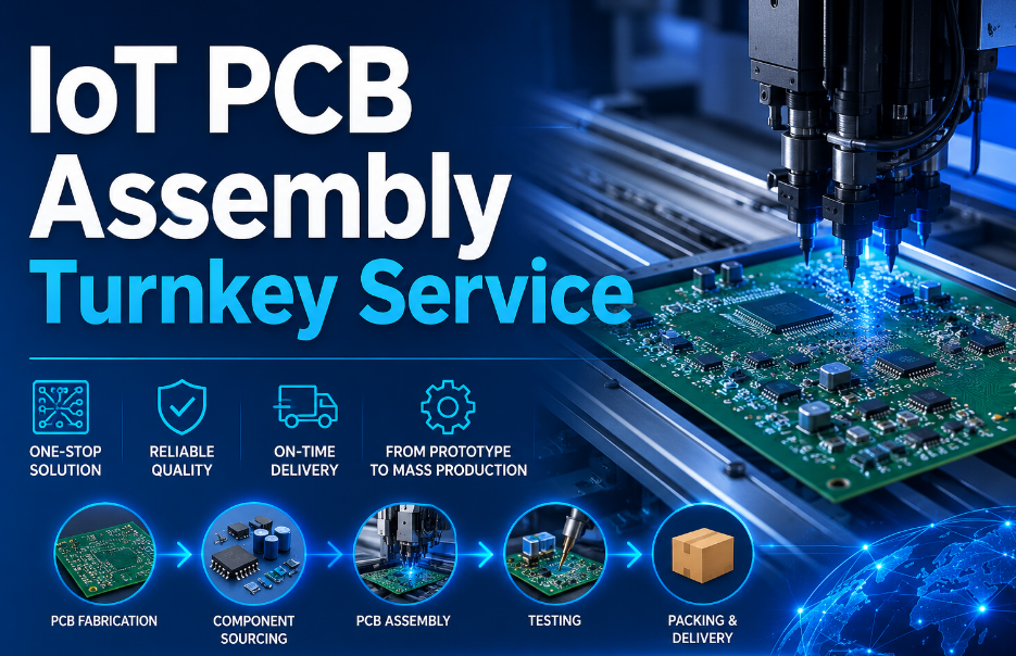
IoT PCB Assembly Turnkey Service, https://www.bestpcbs.com/blog/2026/06/iot-pcb-assembly-turnkey-service/

What Is IoT PCB Assembly Turnkey Service?

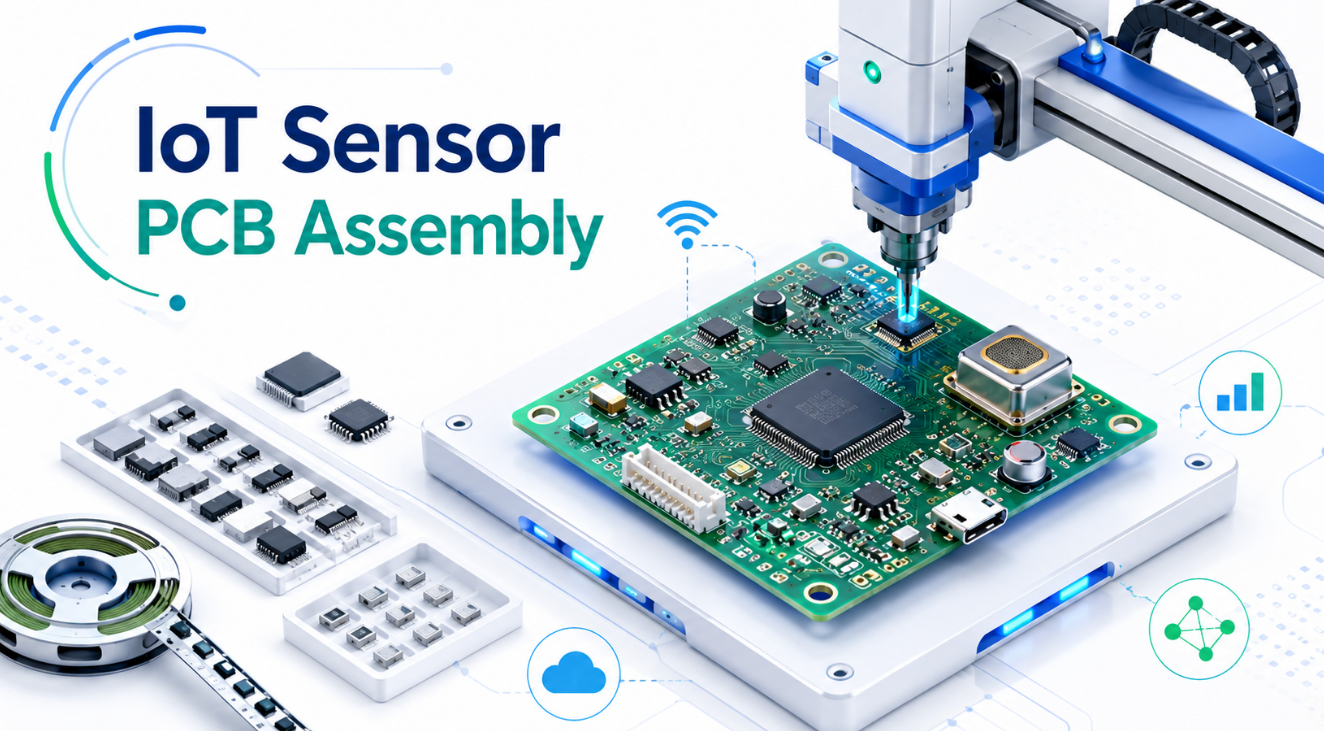
IoT PCB assembly turnkey service is a one-stop PCBA solution for connected electronic products. It covers PCB fabrication, component sourcing, SMT assembly, through-hole assembly, mixed assembly, inspection, testing support, and delivery through one coordinated production flow.

This service is widely used for smart home devices, IoT access control PCB products, wireless sensor boards, industrial IoT modules, gateways, monitoring equipment, and asset tracking devices. These products usually require stable wireless communication, reliable power control, compact placement, and consistent batch quality.

The main advantage of IoT PCB assembly turnkey service is easier project management. Instead of coordinating bare boards, components, soldering, and inspection through separate suppliers, the full PCBA process can be managed through one production partner. This reduces communication gaps and lowers the risk of mismatch between PCB layout, BOM data, component packages, and assembly requirements.

For connected devices, PCBA quality directly affects signal stability, power reliability, operating life, and field performance. A weak assembly process can turn a promising product into a delayed or unreliable launch. That is why choosing a reliable IoT PCBA turnkey solution matters from sample validation to repeat production.

What Does an IoT PCB Assembly Turnkey Service Include?

An IoT PCB assembly turnkey service usually includes everything required to turn approved PCB files and component data into finished IoT PCB assemblies. The goal is to keep PCB production, component preparation, assembly, inspection, and delivery under one organized workflow instead of splitting the project across several separate vendors.

A typical IoT PCB assembly turnkey service project may include:

  • PCB manufacturing preparation
    The process starts with production files, board specifications, stack-up requirements, surface finish, copper weight, solder mask details, and panel requirements. For IoT products, this step helps confirm whether the board is suitable for compact components, RF sections, connectors, and power circuits.
  • BOM review and component preparation
    The BOM is checked for part numbers, package types, values, quantities, polarity, and approved alternatives. This helps reduce the risk of wrong parts, unavailable components, and last-minute sourcing issues before assembly starts.
  • Component sourcing and kitting
    Components can be prepared according to the approved BOM, including ICs, passive components, connectors, modules, sensors, relays, and power devices. Proper kitting helps keep the SMT and through-hole assembly process more stable.
  • SMT assembly
    Surface-mounted components are assembled through solder paste printing, placement, reflow soldering, and inspection. This step is important for IoT boards with dense layouts, fine-pitch packages, wireless modules, and small passive components.
  • Through-hole and mixed assembly
    Connectors, terminals, relays, switches, transformers, and other plug-in components may require through-hole soldering. Many IoT boards use mixed assembly, combining SMT parts with stronger mechanical or power-related components.
  • BGA, QFN, and fine-pitch assembly support
    IoT control boards, gateways, and wireless modules may include BGA, QFN, QFP, or other fine-pitch packages. These components require accurate placement, controlled soldering, and suitable inspection methods.
  • Inspection and testing support
    Inspection may include visual checking, AOI, X-ray inspection for hidden joints, continuity checks, power-on testing, and functional test support. Testing requirements should be confirmed before production so the finished PCBA matches the intended application.
  • Final checking, packing, and delivery
    Finished boards are checked for appearance, quantity, labels, packing method, and order consistency before shipment. This helps protect the assembled boards during transport and reduces problems after arrival.

For IoT access control PCB, smart sensor boards, wireless gateways, and monitoring devices, this full-service model helps reduce project handoff risk. It also makes the path from prototype builds to repeat production easier to manage.

What Types of IoT Products Use Turnkey PCB Assembly?

IoT PCB assembly turnkey service is suitable for IoT products that require stable hardware performance, reliable component sourcing, compact assembly, and repeatable production quality. These products often collect data, control equipment, connect to cloud platforms, or communicate with other smart devices.

Common product types include:

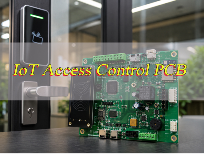
  • IoT access control PCB for smart locks, access terminals, card readers, relay control boards, and smart entry systems.
  • Smart home devices such as thermostats, lighting controllers, security sensors, smart switches, and home gateways.
  • Wireless sensor modules for temperature, humidity, motion, pressure, vibration, gas detection, and environmental monitoring.
  • Industrial IoT devices for machine monitoring, automation control, remote diagnostics, and equipment data collection.
  • Asset tracking devices using GNSS, Bluetooth, LTE, NB-IoT, LoRa, UWB, or other wireless technologies.
  • Smart monitoring systems for energy systems, agriculture, logistics, healthcare equipment, and building control.
  • Gateway and communication modules that connect sensors, edge devices, local networks, and cloud platforms.

These products require more than basic soldering. They require package matching, RF awareness, power stability, inspection discipline, and consistent production records. A well-managed turnkey IoT PCB assembly process helps reduce uncertainty across prototype builds, pilot runs, and repeat production.

What Is the IoT PCB Assembly Turnkey Process?

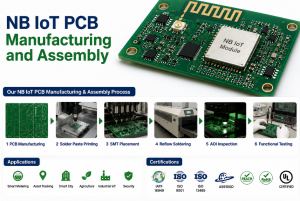
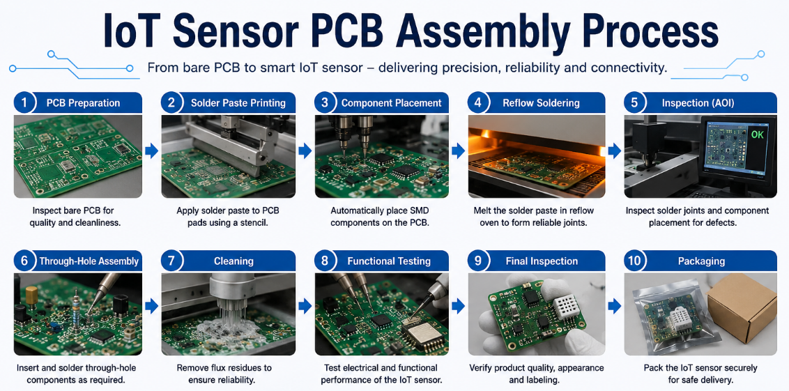
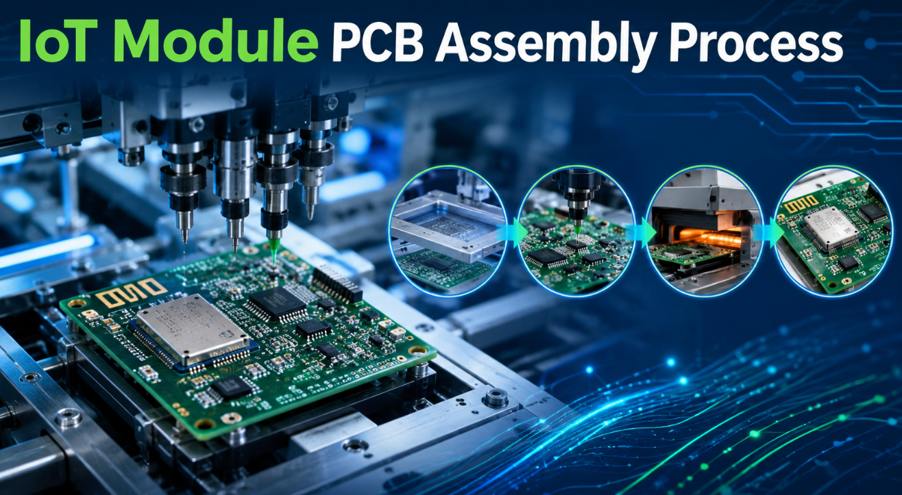
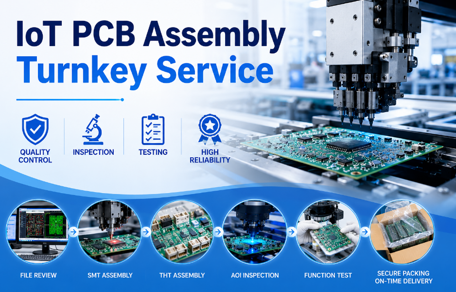
The IoT PCB assembly turnkey service process should be clear, traceable, and easy to manage. A structured process reduces file errors, component mismatches, soldering defects, inspection gaps, and delivery uncertainty. It also helps the project move smoothly from prototype validation to mass production.

1. Project file review
Gerber files, BOM, CPL, assembly drawings, testing notes, and special requirements are reviewed before production starts.

2. DFM and assembly risk check
Footprint matching, component polarity, spacing, fiducials, panel format, soldering risk, and placement direction are checked.

3. PCB fabrication
Bare boards are produced according to material, layer count, copper weight, board thickness, surface finish, solder mask, and tolerance requirements.

4. Component sourcing
Components are prepared based on approved BOM data, manufacturer part numbers, package details, quantities, and substitute rules.

5. SMT assembly
Solder paste printing, component placement, reflow soldering, and AOI inspection are completed for surface-mounted components.

6. Through-hole assembly
Connectors, terminals, relays, switches, transformers, and other plug-in components are assembled with suitable soldering methods.

7. Inspection and testing
AOI, visual inspection, X-ray inspection for hidden joints, and functional testing support are arranged based on project requirements.

8. Final checking and packing
Finished IoT PCB assemblies are checked, labeled, protected with proper packing, and prepared for delivery.

    This process applies to IoT sensor PCB assembly, IoT module PCB assembly, IoT access control PCB assembly, smart device PCBA, and industrial IoT PCB assembly projects. Each step should be confirmed before the next stage begins, especially when the board includes RF modules, power control, or safety-related functions.
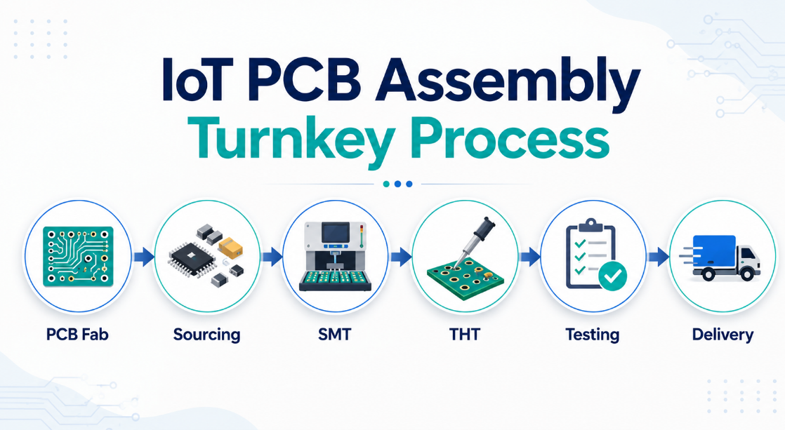
    IoT PCB Assembly Turnkey Process, https://www.bestpcbs.com/blog/2026/06/iot-pcb-assembly-turnkey-service/

    What Files Are Required for an IoT PCB Assembly Turnkey Quote?

    Complete files help the project review move faster and more accurately. For an IoT PCB assembly turnkey service quote, unclear files can cause wrong component selection, assembly delays, polarity mistakes, testing gaps, or repeated confirmation before production.

    The main files include:

    • Gerber files for PCB fabrication.
    • BOM file with reference designator, value, package, quantity, manufacturer part number, and approved alternatives.
    • CPL or pick-and-place file for SMT component position and rotation.
    • Assembly drawing showing polarity, connector direction, special components, and placement notes.
    • PCB specification including material, board thickness, copper weight, surface finish, solder mask color, and impedance requirements.
    • Testing instructions for power-on checks, communication verification, programming, or functional testing.
    • Panel requirements for assembly panel size, breakaway tabs, tooling holes, fiducials, and handling rules.
    • Sample photos or previous version files when the project is based on an existing IoT PCBA.

    For IoT access control PCB projects, extra details can make the review more accurate. These may include relay control requirements, power input range, lock control notes, connector details, communication interfaces, and test procedures. Clear files give production teams a stronger starting point and help reduce avoidable production risk.

    What Should Be Checked Before IoT PCB Assembly Starts?

    Before IoT PCB assembly starts, key production details should be confirmed carefully. IoT boards are often compact and function-heavy, so a small error in polarity, package selection, RF clearance, or connector direction can affect the final device.

    Important checks include:

    • BOM accuracy: part number, value, package, tolerance, voltage rating, and substitute rules.
    • Component polarity: diode, LED, IC, capacitor, connector, module, and relay direction.
    • Footprint matching: PCB pad size and actual component package compatibility.
    • RF section clearance: antenna keep-out area, shielding area, grounding, and impedance-sensitive sections.
    • Power circuit reliability: regulator rating, fuse selection, surge protection, current load, and thermal behavior.
    • Connector alignment: housing fit, cable direction, terminal position, and mechanical clearance.
    • Testing access: test points, programming pads, power input points, and communication interfaces.
    • Panel requirements: board spacing, tooling holes, fiducials, breakaway tabs, and assembly handling.

    These checks are especially important for IoT access control PCB assembly because the same board may manage locks, readers, relays, power modules, and wireless communication. When these details are confirmed early, the PCBA process becomes more predictable and easier to scale.

    What Are Common Challenges in IoT PCB Assembly Turnkey Projects?

    IoT PCB assembly turnkey service projects often involve more variables than standard PCBA orders. Wireless modules, sensors, fine-pitch ICs, connectors, battery circuits, PoE circuits, and mixed assembly components may all appear on one compact board. Without early review, these details can create performance and delivery risks.

    Common challenges include:

    • Component availability changes
      IoT products often use MCUs, wireless modules, sensors, memory chips, and power ICs. Approved substitutes should be discussed early so production can continue smoothly if the original part becomes unavailable.
    • RF signal instability
      Wi-Fi, Bluetooth, GNSS, LoRa, NB-IoT, LTE, and UWB modules may be affected by poor antenna clearance, weak grounding, shielding problems, or contamination near RF sections.
    • Fine-pitch soldering defects
      BGA, QFN, QFP, 01005 components, and dense SMT layouts require accurate placement, stable solder paste printing, controlled reflow, AOI, and X-ray inspection when hidden joints are involved.
    • Power and thermal concerns
      Battery-powered IoT devices, PoE boards, access control systems, and relay-control circuits may face voltage drop, current surge, heat buildup, or connector overload.
    • Testing gaps
      Some IoT PCBA projects require firmware programming, power-on testing, communication checks, relay action checks, and sensor response verification before delivery.
    • Prototype-to-production differences
      A prototype may pass basic validation, but larger production can expose sourcing, panelization, soldering, packing, or testing consistency issues.

    A reliable IoT PCB assembly turnkey service should not only assemble the board but also help identify production risks before they become repeated problems. This is where early file review, component confirmation, inspection control, and clear testing instructions become valuable.

    How Does EBest Control Quality for IoT PCB Assembly Orders?

    EBest controls IoT PCB assembly quality from file review to final shipment, helping reduce assembly errors, rework, delivery risk, and batch inconsistency for IoT products.

    • File review before production
      EBest reviews Gerber files, BOM, CPL, assembly drawings, polarity marks, panel requirements, and testing notes before production starts. This helps identify missing data, footprint mismatches, unclear placement direction, and assembly risks before they affect production.
    • PCB fabrication control
      EBest checks PCB material, board thickness, copper thickness, solder mask, surface finish, hole quality, and board appearance. For IoT access control PCB and wireless IoT boards, stable PCB quality supports reliable power, signal, and mechanical performance.
    • Component verification
      EBest checks component package, value, quantity, polarity, and approved substitute status before assembly. This reduces the risk of wrong parts, unavailable components, or package mismatch in turnkey PCBA projects.
    • SMT process control
      EBest controls solder paste printing, placement accuracy, reflow soldering, and AOI inspection during SMT assembly. This helps reduce solder bridging, tombstoning, shifted components, missing parts, and poor solder joints on compact IoT PCBA.
    • BGA and fine-pitch inspection
      For BGA, QFN, QFP, and fine-pitch components, EBest can arrange X-ray inspection when required. This helps check hidden solder joints that cannot be confirmed by visual inspection alone.
    • Through-hole assembly inspection
      Connectors, relays, terminals, switches, and plug-in parts are checked for solder fill, alignment, pin trimming, and mechanical strength. This is important for IoT access control PCB projects with lock control, relay output, and external wiring.
    • Final inspection before shipment
      EBest checks board appearance, quantity, labels, packing condition, and order consistency before delivery. This helps reduce receiving-side problems and gives the finished PCBA a more reliable delivery condition.
    • Certified quality system support
      EBest holds ISO 9001:2015, ISO 13485:2016, IATF 16949, AS9100D, REACH, RoHS, and UL certifications. These certifications support controlled production for IoT access control PCB, smart sensor PCBA, wireless module PCBA, and industrial IoT PCB assembly projects.

    EBest supports SMT, THT, mixed assembly, BGA assembly, prototype PCB assembly, quick turn PCB assembly, and full turnkey PCB assembly. Its assembly capability includes 01005 minimum SMD components, 0.25 mm minimum BGA pitch, and component handling for reels, cut tape, tube, tray, and loose parts.
    IoT PCB Assembly Turnkey Service, https://www.bestpcbs.com/blog/2026/06/iot-pcb-assembly-turnkey-service/

    How Does EBest Support IoT PCB Prototyping and Mass Production?

    EBest supports IoT PCB projects from early sample builds to repeat production, helping projects verify function, improve assembly details, and scale with better production consistency.

    • Prototype PCB assembly for early validation
      EBest supports small-batch prototype PCB assembly for checking board function, soldering quality, connector fit, programming access, RF behavior, and power performance before larger production begins.
    • Quick turn support for urgent validation
      When an IoT project is under schedule pressure, EBest can support quick turn PCB assembly based on file readiness, component availability, and production complexity. This helps shorten the sample testing cycle.
    • BOM and component review before scaling
      EBest checks BOM details, package matching, substitute options, and sourcing risks before production volume increases. This helps prevent last-minute component problems during batch production.
    • Assembly feedback during prototype builds
      EBest can identify practical risks such as tight component spacing, difficult soldering areas, unclear polarity marks, weak panel format, or limited testing access. These findings help improve the next production version.
    • Stable production records for repeat orders
      Once the prototype is approved, EBest can keep production notes, component information, inspection requirements, and packing standards consistent. This helps reduce variation across different production batches.
    • Mass production workflow control
      For larger orders, EBest focuses on stable sourcing, SMT process control, through-hole assembly quality, inspection discipline, final checking, and delivery coordination. This supports long-term IoT PCBA production with fewer unexpected interruptions.
    • Broad IoT product coverage
      EBest can support IoT access control PCB, wireless sensor PCBA, smart home PCBA, gateway modules, asset tracking boards, industrial IoT PCBA, and smart monitoring device assemblies.

    This support helps an IoT PCB assembly turnkey service project move from sample approval to mass production without changing suppliers, rebuilding communication, or losing key production details.

    How Does EBest Ensure On-Time Delivery for IoT PCBA Projects?

    EBest improves delivery control by managing PCB fabrication, component sourcing, SMT assembly, through-hole assembly, inspection, and packing through one coordinated workflow. This makes IoT PCB assembly turnkey service projects easier to schedule and easier to track.

    • Early file confirmation
      EBest checks Gerber files, BOM, CPL, assembly drawings, panel requirements, and testing notes before production scheduling. This helps prevent delays caused by missing files or unclear instructions.
    • Component sourcing coordination
      EBest reviews component availability, package details, approved substitutes, and sourcing risks. For IoT PCBA orders, this helps reduce the chance of production being delayed by one missing MCU, module, connector, or power IC.
    • PCB and PCBA schedule planning
      EBest coordinates PCB fabrication, component preparation, SMT assembly, through-hole assembly, inspection, and packing based on project complexity. This keeps each stage better aligned.
    • Quick turn assembly support
      For prototype and low-volume IoT PCBA projects, EBest can support quick turn assembly depending on material readiness and production requirements. This helps speed up urgent validation and early project stages.
    • Production tracking across key stages
      EBest follows the order from PCB fabrication to SMT, THT, inspection, packing, and delivery preparation. Clear tracking helps reduce uncertainty during production.
    • Final checking before shipment
      EBest checks appearance, quantity, labels, packing, and order consistency before shipment. This helps avoid preventable delivery-side issues.
    • Capacity support for prototype and repeat orders
      EBest has monthly PCB capability of about 260,000 square feet / 28,900 square meters. Assembly lead time can reach 1–5 days, depending on project conditions, material readiness, and production complexity.

    For IoT access control PCB, sensor boards, wireless modules, and smart device PCBA projects, this delivery approach helps improve schedule predictability and reduce production interruptions.

    Why Choose EBest for IoT PCB Assembly Turnkey Service?

    EBest provides IoT PCB assembly turnkey service for smart devices, IoT access control PCB, wireless modules, sensor boards, gateways, and industrial connected equipment.

    • One-stop service reduces project complexity
      EBest covers PCB fabrication, component sourcing, SMT assembly, through-hole assembly, mixed assembly, inspection, testing support, and box assembly. This helps reduce the effort of coordinating several separate production links.
    • Strong PCBA capability for compact IoT products
      EBest supports 01005 SMD components, 0.25 mm BGA pitch, BGA assembly, QFN/QFP packages, mixed assembly, and multiple component supply formats. This is suitable for compact IoT boards with dense layouts and fine-pitch components.
    • Prototype-to-mass-production support
      EBest supports prototype PCB assembly, quick turn PCB assembly, and full turnkey PCB assembly. This helps projects verify samples, improve assembly details, and move into repeat orders more smoothly.
    • Wide PCB fabrication capability
      EBest can support FR4 PCB, multilayer PCB, flexible PCB, rigid-flex PCB, ceramic PCB, metal-based PCB, and high-frequency PCB. This gives IoT projects more flexibility when board structure, thermal performance, signal requirements, or size constraints change.
    • Quality certifications support production confidence
      EBest holds ISO 9001:2015, ISO 13485:2016, IATF 16949, AS9100D, REACH, RoHS, and UL. These certifications support controlled production for projects that require stable quality and documented manufacturing standards.
    • More than 19 years of PCB and PCBA experience
      EBest understands common production risks in IoT PCB assembly projects, including BOM issues, component sourcing risk, SMT defects, connector reliability, RF-sensitive areas, and batch consistency.
    • Value-added services support complete product delivery
      In addition to PCBA, EBest can support box assembly, injection molding, CNC machining, sheet metal, cable connection, labeling, and final assembly options. This is useful when an IoT project requires more than bare PCBA delivery.
    • Clear communication improves project efficiency
      EBest helps review files, confirm production details, coordinate sourcing, manage assembly, and arrange inspection. This gives the project a more organized path from technical files to finished IoT PCB assemblies.

    Choosing EBest means the project can get PCB fabrication, sourcing, assembly, inspection, delivery coordination, and value-added support from one experienced PCBA partner.
    IoT PCB Assembly Turnkey Service, https://www.bestpcbs.com/blog/2026/06/iot-pcb-assembly-turnkey-service/

    FAQs About IoT PCB Assembly Turnkey Service

    Q1: Can EBest assemble IoT PCBA with small-size components and fine-pitch packages?
    A1: Yes. EBest supports compact IoT PCBA with 01005 minimum SMD components and 0.25 mm minimum BGA pitch. This is suitable for wireless modules, sensor boards, smart control boards, and IoT access control PCB projects with limited PCB space.

    Q2: Can EBest handle both SMT and through-hole parts on the same IoT board?
    A2: Yes. EBest supports SMT, THT, and mixed assembly for IoT PCBA projects. This is useful when one board includes ICs, wireless modules, sensors, connectors, terminals, relays, and other plug-in components.

    Q3: What component package formats can EBest work with?
    A3: EBest can handle components supplied in reels, cut tape, tube, tray, and loose parts. This gives turnkey IoT PCB assembly projects more flexibility when different component types are used in one BOM.

    Q4: Can EBest support urgent IoT prototype assembly?
    A4: Yes. EBest supports quick turn PCB assembly, and assembly lead time can reach 1–5 days, depending on file readiness, component availability, quantity, testing requirements, and production complexity.

    Q5: What PCB materials or board types can be used for IoT products?
    A5: EBest supports FR4 PCB, multilayer PCB, flexible PCB, rigid-flex PCB, ceramic PCB, metal-based PCB, and high-frequency PCB. These options help match different IoT requirements such as compact structure, RF performance, thermal control, and mechanical flexibility.

    Q6: Can EBest help if the IoT product requires enclosure or final assembly support?
    A6: Yes. Besides PCBA, EBest can support box assembly, injection molding, CNC machining, sheet metal, cable connection, labeling, and final assembly. This is helpful when the project requires more than bare PCBA delivery.

    Q7: What certifications support EBest’s IoT PCB assembly service?
    A7: EBest holds ISO 9001:2015, ISO 13485:2016, IATF 16949, AS9100D, REACH, RoHS, and UL. These certifications support controlled production for IoT access control PCB, wireless module PCBA, sensor board PCBA, and industrial IoT PCB assembly projects.

    Q8: Can EBest support repeat IoT PCBA orders after the prototype is approved?
    A8: Yes. EBest supports prototype PCB assembly, quick turn PCB assembly, full turnkey PCB assembly, and repeat production. With monthly PCB capability of about 260,000 square feet / 28,900 square meters, EBest can support both sample validation and long-term IoT PCBA production.

    Request a Fast Quote for Your IoT PCB Assembly Turnkey Project

    EBest provides IoT PCB assembly turnkey service for IoT access control PCB, wireless modules, smart sensor boards, gateways, tracking devices, and industrial connected equipment. From PCB fabrication and component sourcing to SMT assembly, through-hole assembly, mixed assembly, inspection, and delivery support, EBest helps turn your IoT PCB project into reliable finished PCBA.

    Send your Gerber files, BOM, CPL, assembly notes, testing requirements, and quantity plan to sales@bestpcbs.com. EBest will review your project and provide a customized IoT PCBA turnkey solution with reliable quality, professional communication, and dependable production support.
    You may also like

    IoT Sensor PCB Assembly Services for Smart Monitoring and Wireless Devices

    June 4th, 2026

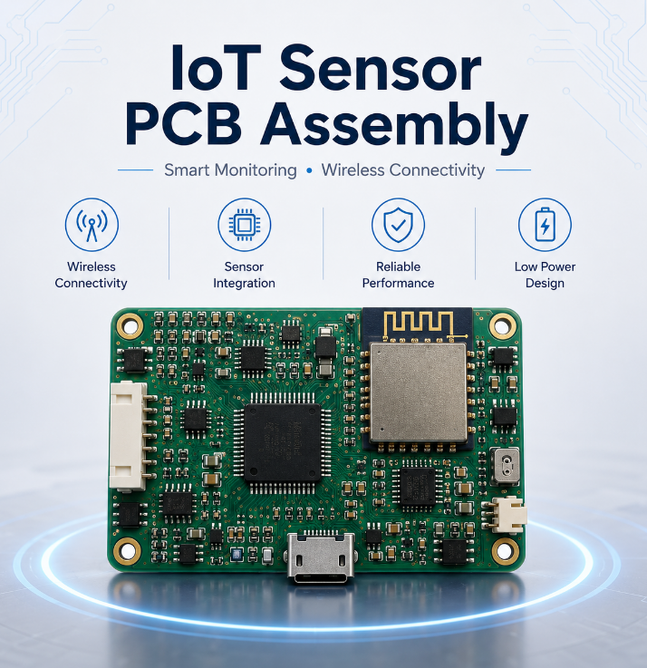
    Looking for reliable IoT sensor PCB assembly for smart monitoring and wireless devices? A qualified IoT sensor PCBA must support accurate sensing, stable wireless transmission, low power consumption, and long-term field reliability. It is commonly used in smart buildings, industrial monitoring, asset tracking, agriculture, security devices, energy systems, and wearable electronics.

    In real production, small assembly issues can quickly affect the whole device. Poor soldering, wrong sensor placement, weak RF control, unstable power supply, or missing test points may cause data errors, short battery life, weak signal, or delivery delays. This article explains the key components, assembly process, quality control, testing requirements, common problems, and supplier selection points for IoT sensor PCB assembly.

    IoT Sensor PCB Assembly, https://www.bestpcbs.com/blog/2026/06/iot-sensor-pcb-assembly/

    What Is IoT Sensor PCB Assembly?

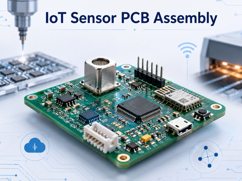
    IoT sensor PCB assembly is the process of mounting and soldering sensors, wireless modules, MCUs, power circuits, connectors, and protection components onto a printed circuit board. After assembly, the board can collect data, process signals, transmit information, and work as the electronic core of a smart monitoring device.

    Unlike standard PCB assembly, IoT sensor PCB assembly must consider sensor accuracy, RF performance, power consumption, firmware loading, and functional testing at the same time. A small error in sensor placement, antenna area, soldering quality, or power circuit control can affect data stability and wireless communication.

    A complete IoT sensor PCBA project usually includes PCB fabrication, component sourcing, SMT assembly, through-hole assembly if required, inspection, programming, testing, and final packaging. For smart monitoring and wireless devices, the goal is not only to assemble components correctly, but also to make the board stable, testable, and ready for real application use.

    Where Is IoT Sensor PCB Assembly Used in Smart Monitoring Devices?

    IoT sensor PCB assembly is used in products that collect real-world data and send it to a gateway, cloud platform, mobile app, or control system. These products are common in smart buildings, industrial monitoring, logistics, agriculture, medical electronics, energy systems, and security devices.

    Main application areas include:

    • Smart buildings: air quality monitoring, occupancy detection, lighting control, HVAC monitoring
    • Industrial monitoring: vibration monitoring, machine status detection, energy tracking
    • Logistics: cold chain monitoring, GPS tracking, shock detection, humidity tracking
    • Agriculture: soil monitoring, weather stations, irrigation control
    • Security devices: motion detection, door sensors, smart alarms
    • Medical and wearable devices: portable monitoring, body temperature, motion sensing

    Each application has different requirements for sensor accuracy, wireless range, power consumption, board size, and environmental protection. Therefore, the assembly plan should match the final working environment before production starts.

    What Components Are Used in IoT Sensor PCB Assembly?

    An IoT sensor PCBA usually combines sensing, control, communication, power, storage, connection, and protection circuits. Each part affects final device performance, so BOM accuracy and component quality should be reviewed before production.

    CategoryExamplesFunction
    Sensor UnitTemperature, humidity, vibration, gas, pressureData collection
    MCUSTM32, ESP32, Nordic, NXP, TISignal processing
    Wireless ModuleWi-Fi, BLE, LoRa, NB-IoT, LTE-M, ZigbeeData transmission
    Power CircuitLDO, DC-DC, PMIC, charger ICVoltage control
    MemoryFlash, EEPROMData storage
    ConnectorUSB-C, FPC, board-to-board, pin headerExternal connection
    ProtectionTVS, ESD diode, fuse, surge protectorCircuit safety

    Many IoT sensor boards use compact packages such as 0201, 0402, QFN, LGA, BGA, and fine-pitch ICs. Because of this, solder paste volume, SMT placement accuracy, and reflow profile control directly affect assembly quality.

    Before batch production, component lifecycle and supply stability should also be reviewed. If a sensor IC, wireless module, or MCU has a long lead time, an approved alternative can help protect the production schedule.

    Which Sensors Are Commonly Used in Smart Monitoring Devices?

    Smart monitoring devices use different sensors according to the data they collect. The sensor choice depends on the application, working environment, accuracy level, power consumption, and enclosure structure.

    Common sensor types include:

    • Environmental sensors: temperature, humidity, air quality, CO2, PM2.5, VOC, light, pressure
    • Industrial sensors: vibration, current, proximity, flow, tilt, magnetic, acceleration
    • Security sensors: PIR motion sensor, reed switch, light sensor, sound sensor
    • Wearable sensors: pressure, motion, body temperature, pulse-related sensing
    • Agriculture sensors: soil moisture, pH, light, water level, outdoor temperature

    Sensor placement must be handled carefully during IoT sensor PCB assembly. Heat sources, blocked airflow, vibration direction, RF circuits, and enclosure openings can all affect measurement accuracy.

    What Wireless Functions Should an IoT Sensor PCB Support?

    Wireless function allows the IoT sensor board to send collected data to another device or platform. Common wireless options include Wi-Fi, BLE, LoRa, NB-IoT, LTE-M, Zigbee, Sub-GHz, and proprietary RF communication.

    Wireless TypeCommon UseKey Concern
    Wi-FiSmart home, gateway devicesHigher power use
    BLEWearables, short-range sensorsBattery life
    LoRaOutdoor and remote monitoringAntenna tuning
    NB-IoT / LTE-MAsset tracking, smart metersPeak current
    ZigbeeSmart building systemsNetwork stability
    Sub-GHzIndustrial and security devicesRF range

    For wireless IoT sensor PCB assembly, antenna clearance and RF layout are critical. The antenna area should avoid metal parts, batteries, screws, dense copper, and enclosure blockage.

    Poor RF control can cause weak signal, unstable connection, higher retry rate, and shorter battery life. Therefore, wireless module placement, RF matching, shielding, and enclosure influence should be reviewed before production.

    What Should Be Checked Before IoT Sensor PCB Assembly?

    Before IoT sensor PCB assembly starts, production files and key requirements should be checked clearly. This helps reduce wrong parts, soldering errors, testing delays, and unstable device performance.

    Key items to confirm include:

    • Gerber files: PCB layers, drill files, solder mask, silkscreen, outline, and surface finish
    • BOM: part number, package, value, tolerance, quantity, and replacement options
    • Pick-and-place file: component position, rotation, polarity, and reference designator
    • Assembly drawing: connector direction, special parts, manual soldering notes, and label position
    • Sensor area: heat source distance, airflow path, exposure window, and mounting direction
    • Wireless area: antenna keep-out, RF matching circuit, grounding, and enclosure influence
    • Test points: power rails, programming port, communication interface, and sensor signals

    For compact sensor boards, small file errors can cause major production problems. Polarity, footprint, antenna clearance, and test access should be checked before assembly begins.

    IoT Sensor PCB Assembly, https://www.bestpcbs.com/blog/2026/06/iot-sensor-pcb-assembly/

    What Is the IoT Sensor PCB Assembly Process?

    The IoT sensor PCB assembly process should be controlled from file review to final testing. Sensor boards often combine small components, wireless modules, low-power circuits, and sensitive sensor areas, so each step must be clear and traceable.

    Step 1: Review files and BOM
    Gerber files, BOM, pick-and-place files, and assembly drawings are checked before production. This step helps find wrong footprints, missing polarity marks, unavailable components, unclear connector directions, and possible soldering risks.

    Step 2: Prepare PCB and components
    The bare PCB is fabricated according to board thickness, surface finish, solder mask, and stack-up requirements. Components are checked by part number, package, quantity, moisture level, and storage condition before SMT production.

    Step 3: Print solder paste
    Solder paste is printed onto PCB pads through a stencil. For compact IoT sensor boards, paste volume and alignment must be controlled carefully because fine-pitch ICs and small passive parts are sensitive to excess or insufficient solder.

    Step 4: Place SMT components
    SMT machines place sensors, MCUs, wireless modules, power ICs, resistors, capacitors, and connectors onto the PCB. Accurate placement is important for 0201, 0402, QFN, LGA, BGA, and fine-pitch components.

    Step 5: Complete reflow soldering
    The board passes through a controlled reflow oven to form solder joints. A proper reflow profile helps reduce solder bridges, tombstoning, poor wetting, component shifting, and thermal damage to sensitive parts.

    Step 6: Add secondary assembly
    If the board includes through-hole connectors, terminals, battery holders, shield cans, or special mechanical parts, secondary assembly is arranged. This may include manual soldering, selective soldering, or fixture-assisted assembly.

    Step 7: Inspect, program, and test
    After soldering, the board goes through AOI, visual inspection, X-ray if required, firmware loading, functional testing, wireless testing, sensor response checking, and final inspection before shipment.

    IoT Sensor PCB Assembly process, https://www.bestpcbs.com/blog/2026/06/iot-sensor-pcb-assembly/

    What Quality Controls Are Needed During IoT Sensor PCB Assembly?

    Quality control for IoT sensor PCB assembly should focus on soldering quality, component direction, RF area, sensor position, and powered performance. These are the areas most likely to affect final device reliability.

    Incoming material inspection
    PCBs and components should be checked before production. This includes part number, package, quantity, appearance, moisture status, and storage condition. This step helps avoid wrong parts, damaged components, and moisture-related soldering issues.

    Solder paste inspection
    SPI checks solder paste height, area, volume, and position before placement. This is useful for fine-pitch ICs, QFN packages, small passive components, and dense layouts where paste defects can quickly cause solder bridges or open joints.

    SMT placement control
    Placement control checks position, rotation, polarity, and package matching. Sensors, LEDs, diodes, ICs, wireless modules, and connectors must be mounted in the correct direction because one polarity error can cause board failure.

    Reflow profile control
    The reflow profile should match solder paste type, PCB thickness, component size, and thermal sensitivity. Good profile control improves solder joint consistency and reduces tombstoning, voids, poor wetting, and heat damage.

    AOI and X-ray inspection
    AOI checks visible defects such as missing parts, wrong polarity, offset parts, and solder bridges. X-ray is useful for QFN, BGA, LGA, and hidden solder joints where surface inspection cannot show the full solder condition.

    Process traceability
    For batch production, component lot records, inspection results, testing data, and production feedback should be traceable. This makes quality control clearer and helps locate the root cause quickly if an issue appears later.

    What Testing Is Required for IoT Sensor PCB Assembly?

    Testing is important because many problems in IoT sensor PCB assembly only appear after the board is powered, programmed, and connected. A clear test plan helps verify sensor response, wireless communication, power stability, and product function.

    Basic electrical test
    Electrical testing checks shorts, opens, power rails, voltage output, resistance values, and current draw. It helps find solder bridges, wrong components, missing parts, and power circuit problems before full function testing.

    Power consumption test
    Many IoT sensor devices are battery-powered, so current should be measured in different states. Standby current, sleep current, wake-up current, peak current, and wireless transmission current can directly affect battery life.

    Firmware loading test
    Firmware loading confirms that the MCU or wireless module can be programmed correctly. Programming pads, boot mode, reset pin, communication interface, and flash memory should be checked during this step.

    Sensor function test
    Sensor testing verifies whether the board can collect correct data. Depending on the product, this may include temperature response, humidity response, pressure signal, motion detection, vibration response, gas output, or light sensing.

    Wireless communication test
    Wireless testing checks pairing, signal strength, transmission response, antenna performance, and connection stability. This is important for Wi-Fi, BLE, LoRa, NB-IoT, LTE-M, Zigbee, and Sub-GHz sensor boards.

    Calibration test
    Some sensors require calibration after assembly to improve accuracy. This is common for gas sensors, pressure sensors, humidity sensors, temperature sensors, and current sensors. Calibration standards and acceptance ranges should be clear before production.

    Final functional test
    Final testing should simulate basic product operation. It may include power-on test, data upload test, LED or button test, connector test, relay output test, wireless response test, and sensor reading verification.

    What Common Problems Occur in IoT Sensor PCB Assembly Projects?

    IoT sensor PCB assembly projects often face issues in sensor accuracy, wireless signal, power stability, soldering quality, firmware loading, and field reliability. These problems should be reviewed before batch production to reduce rework and delivery risk.

    Unstable sensor data
    Unstable data is often caused by poor grounding, heat interference, blocked airflow, wrong sensor direction, or nearby noisy circuits. Temperature sensors should stay away from heat sources, and gas or humidity sensors should have proper exposure to airflow.

    Weak wireless signal
    Weak signal may happen when the antenna area is blocked by copper, batteries, screws, metal housings, shield cans, or dense components. Antenna clearance, RF matching, module placement, and enclosure influence should be checked before production.

    Short battery life
    Battery-powered sensor devices may drain quickly if sleep current is high, the regulator is inefficient, or wireless transmission consumes too much current. Standby current, peak current, charger circuit, and wake-up timing should be tested.

    Soldering defects
    Fine-pitch ICs, QFN packages, small passive parts, and compact layouts can increase the risk of solder bridges, open joints, tombstoning, voids, and poor wetting. Stencil design, paste printing, placement accuracy, and reflow control help reduce these problems.

    Sensor drift after assembly
    Sensor drift can appear when the sensor is too close to heat-generating components, airflow is blocked, or calibration is missing. Proper placement and calibration help improve consistency for temperature, humidity, gas, pressure, and current sensors.

    Programming or boot failure
    Programming failure may come from wrong firmware, unstable power rails, poor contact with programming pads, missing boot mode control, or unclear test instructions. Clear programming files and stable test access make production testing more reliable.

    Moisture and environmental damage
    Boards used outdoors, in factories, warehouses, agriculture, or humid environments may face moisture, dust, vibration, and corrosion. Conformal coating, clean soldering, stronger connector control, and reliability testing can improve field performance.

    How to Choose a Reliable IoT Sensor PCB Assembly Manufacturer?

    A reliable IoT sensor PCB assembly manufacturer should control more than SMT placement. The right partner should understand sensors, wireless modules, low-power circuits, compact layouts, and testing requirements.

    Check sensor assembly experience
    The manufacturer should understand how sensor position affects data accuracy. Temperature sensors should stay away from heat sources, while humidity, gas, and air quality sensors should have proper exposure to airflow.

    Confirm wireless module capability
    For Wi-Fi, BLE, LoRa, NB-IoT, LTE-M, Zigbee, or Sub-GHz boards, the manufacturer should check antenna clearance, RF area, module placement, and enclosure influence before production.

    Review SMT production ability
    IoT sensor PCBAs often use 0201, 0402, QFN, LGA, BGA, fine-pitch ICs, and compact connectors. The manufacturer should support accurate solder paste printing, SMT placement, reflow control, AOI, and X-ray inspection when required.

    Ask about BOM and sourcing review
    A good manufacturer should check part numbers, package types, lead time, lifecycle status, and possible alternatives before assembly. This helps reduce wrong parts, material delays, and risky substitutions.

    Confirm testing support
    The manufacturer should support firmware loading, power rail checking, functional testing, wireless communication testing, current measurement, and sensor response testing according to project requirements.

    Check prototype and batch support
    Prototype assembly helps verify function and assembly feasibility. Batch production requires stable process control, repeatable testing, material consistency, and clear inspection records.

    Evaluate communication quality
    Choose a manufacturer that gives clear feedback on missing files, unclear drawings, risky components, missing test points, and assembly concerns. Clear feedback helps avoid delays and rework.

    Prefer one-stop PCB and PCBA service
    For IoT sensor PCB assembly projects, one-stop support for PCB fabrication, SMT assembly, sourcing, inspection, programming, and testing can reduce communication gaps and make production easier to control.

    Why Choose EBest for IoT Sensor PCB Assembly Services?

    EBest provides IoT sensor PCB assembly services for smart monitoring devices, wireless modules, industrial sensing products, smart home devices, tracking systems, and connected electronic products. Our service covers PCB fabrication, SMT assembly, component sourcing, inspection, testing, and production support.

    One-stop PCB and PCBA support
    EBest can support PCB fabrication, SMT assembly, component sourcing, through-hole assembly, inspection, and testing in one workflow. This helps reduce separate communication steps and makes project coordination more efficient.

    Support for compact IoT sensor boards
    Many IoT sensor boards use fine-pitch ICs, small passive components, wireless modules, shield cans, compact connectors, and sensitive sensors. EBest focuses on stable SMT placement, accurate soldering, controlled reflow profiles, and reliable inspection.

    Practical review before assembly
    Before production, EBest can review assembly risk, BOM availability, test points, wireless module placement, sensor position, and quality requirements. This helps reduce preventable production issues and improves batch consistency.

    Testing support for connected devices
    EBest can provide AOI inspection, X-ray inspection, firmware loading support, functional testing, wireless testing support, visual inspection, and packaging control according to project requirements. These steps help improve delivery reliability for smart monitoring and wireless devices.

    Prototype to batch production support
    EBest supports both prototype samples and batch production. Early samples help verify function and assembly feasibility, while batch production focuses on repeatable process control, stable quality, and reliable delivery.

    IoT Sensor PCB Assembly Services, https://www.bestpcbs.com/blog/2026/06/iot-sensor-pcb-assembly/

    FAQs About IoT Sensor PCB Assembly

    Q1: Can I send only partial files first for an initial review?
    A1: Yes. You can send available files first, such as Gerber files, BOM, or sample photos. For a formal quotation, Gerber, BOM, pick-and-place file, quantity, and testing notes will make the quote more accurate.

    Q2: Can one project include several PCB revisions?
    A2: Yes. If your project has different versions, mark each revision clearly in the file name and BOM. This helps avoid mixing old and new files during production.

    Q3: Can assembled boards be packed for direct device integration?
    A3: Yes. EBest can arrange anti-static bags, trays, labels, barcode stickers, moisture protection, and export packaging according to the project requirements.

    Q4: Can EBest support repeat orders after the first batch?
    A4: Yes. Repeat orders can be supported with saved production data, BOM records, process notes, and inspection requirements. This helps make later batches more consistent.

    Q5: Can special labels or serial numbers be added?
    A5: Yes. Labels, serial numbers, QR codes, and batch tracking marks can be added when the label format and location are provided before production.

    Q6: Can EBest help with urgent project schedules?
    A6: Yes. Urgent schedules can be reviewed based on PCB complexity, component availability, testing scope, and quantity. Clear files and confirmed components help speed up production planning.

    Get a Fast Quote for Your IoT PCB Assembly Project

    Ready to move your IoT PCB assembly project forward? Send your Gerber files, BOM, pick-and-place file, quantity, and special requirements to sales@bestpcbs.com. If your board includes sensors, wireless modules, firmware loading, coating, calibration, or custom packaging, include these details so we can prepare a more accurate quote.

    EBest will review your project files and reply with practical production advice, clear cost information, and a suitable assembly plan. Whether your project is for smart monitoring devices, wireless sensor modules, industrial sensing products, or connected electronic boards, we can help you start production with fewer communication gaps and better quality control.

    Share your project details now, and our team will help you confirm the next production step quickly and professionally.

    You may also like

    IoT Module PCB Assembly Service for Smart Devices

    June 4th, 2026

    Is IoT module PCB assembly slowing your smart device project? A smart device may look simple from the outside, but the PCB inside must handle power control, wireless communication, signal stability, data processing, and long-term operation at the same time.

    That is why IoT module PCB assembly should be planned carefully from the first sample stage. A stable assembly process helps reduce production problems, improve product reliability, and make repeat orders easier to control.

    IoT Module PCB Assembly, https://www.bestpcbs.com/blog/2026/06/iot-module-pcb-assembly/

    What Is IoT Module PCB Assembly?

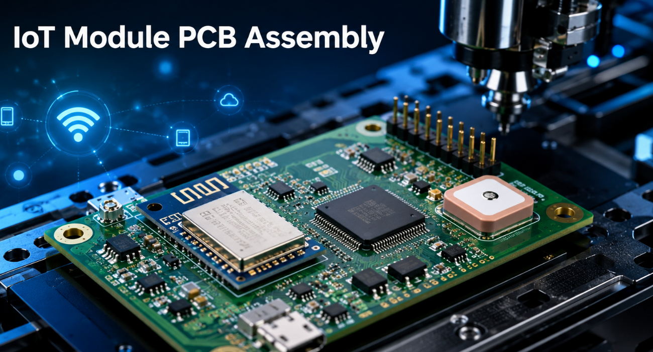
    IoT module PCB assembly is the process of mounting electronic components onto PCB boards used in smart connected devices. These boards usually include wireless modules, GPS modules, sensors, control chips, power circuits, connectors, antennas, shielding parts, and power interfaces.

    The PCB works as the main connection platform of the device. After components are assembled onto the board, the device can collect data, send signals, receive commands, track location, and work in real operating conditions.

    A complete IoT module PCB assembly service usually includes:

    • PCB fabrication for board structure, layer count, copper weight, solder mask, and surface finish
    • Component sourcing based on BOM, package, part number, and supply availability
    • SMT assembly for ICs, wireless modules, sensors, and passive components
    • Through-hole assembly for connectors, terminals, pin headers, and mechanical parts
    • Shielding assembly for GPS, RF, wireless, and EMI-sensitive areas
    • Inspection and functional testing before shipment
    • Cleaning, labeling, packaging, and delivery support

    For products using Bluetooth, WiFi, LoRa, NB-IoT, LTE-M, GPS, GNSS, or other wireless functions, assembly quality can affect signal strength, battery life, connection stability, and final product performance.

    What Smart Devices Use IoT Module PCB Assembly?

    Many smart devices use IoT module PCB assembly because they rely on wireless communication, sensing, tracking, or remote control. These devices are usually compact, but the PCB inside must support several functions at once.

    Common applications include:

    • GPS trackers: Used for vehicle tracking, asset tracking, fleet management, personal location devices, and anti-theft products.
    • Smart meters: Used in electricity meters, water meters, gas meters, and energy monitoring systems.
    • Industrial sensors: Used for temperature, pressure, vibration, humidity, motion, and equipment status monitoring.
    • Smart home controllers: Used in lighting control, door locks, HVAC systems, alarms, and appliance control.
    • Wearable devices: Used in health monitoring, sports tracking, portable electronics, and personal safety devices.
    • Wireless gateways: Used to collect data from sensors and send it to cloud platforms or control systems.
    • Medical monitoring terminals: Used in portable medical devices, remote monitoring equipment, and connected healthcare products.
    • Security devices: Used in access control systems, alarms, surveillance terminals, and smart entry devices.
    • Vehicle tracking units: Used in logistics, fleet systems, shared mobility, and transportation monitoring.

    In these products, the PCB board is more than a carrier for components. It manages power, sensors, wireless communication, signal transmission, and cloud connection.

    Why Do IoT Modules Require Reliable PCB Assembly?

    IoT modules require reliable PCB assembly because they often run continuously and communicate wirelessly in real environments. Some devices are installed outdoors, inside machines, in vehicles, or in locations where repair is difficult.

    Main reasons include:

    • Long working time: Many IoT devices run day and night, so weak solder joints or unstable components may cause failure over time.
    • Wireless dependence: Poor assembly may reduce signal strength, connection range, data transmission, or GPS positioning.
    • Compact board space: Small layouts make component placement, soldering, and inspection more sensitive.
    • Field operation: Devices may face vibration, heat, humidity, dust, unstable voltage, or battery power changes.
    • Repair difficulty: Once a device is installed, replacement or rework can cost more than proper assembly control.
    • Batch consistency: Repeat orders should perform the same as approved samples, especially when products are shipped in volume.

    Reliability starts from small production details. Solder paste printing, SMT placement, reflow temperature, polarity checking, board cleaning, inspection, and testing all influence the final result.

    What Components Are Commonly Used in IoT Module PCB Boards?

    IoT module PCB boards use many small and functional components. Each part has a clear job, and all parts must work together after assembly.

    Common components include:

    • MCU or processor: Controls data processing, system logic, device operation, and communication commands.
    • Wireless module: Supports Bluetooth, WiFi, Zigbee, LoRa, NB-IoT, LTE-M, 4G, or other communication functions.
    • GPS/GNSS module: Provides positioning, navigation, tracking, and location data.
    • SIM card slot or eSIM interface: Used for cellular IoT products with mobile network access.
    • Antenna connector: Connects internal or external antennas for GPS, cellular, WiFi, or LoRa functions.
    • Crystal oscillator: Supports stable timing for communication modules and control circuits.
    • Power IC: Manages voltage conversion, charging, protection, and stable power supply.
    • Sensors: Collect temperature, pressure, motion, humidity, light, vibration, or other data.
    • Passive components: Include resistors, capacitors, inductors, diodes, filters, and protection parts.
    • Connectors and terminals: Support power input, data connection, programming, debugging, and external interfaces.
    • Shielding cover: Helps reduce EMI and protect sensitive RF or wireless areas.
    • Battery interface: Supports portable, low-power, rechargeable, or backup-power IoT products.
    • LED indicator or buzzer: Provides basic status indication, alarm signals, or device feedback.

    Many IoT boards use fine-pitch packages such as QFN, BGA, LGA, DFN, and small passive components like 0201 or 0402. These parts require accurate SMT placement, proper stencil control, stable reflow soldering, and careful inspection.

    What Wireless Functions Should an IoT Module PCB Support?

    An IoT module PCB should support wireless functions based on working distance, power consumption, data rate, and application environment. Different wireless technologies bring different assembly and testing requirements.

    Common wireless functions include:

    • Bluetooth: Used for short-range connection in wearables, sensors, smart locks, and portable devices. It is often used when the device works close to a phone, gateway, or control terminal.
    • WiFi: Used for smart home devices, gateways, cameras, and control terminals. It supports higher data speed but requires stable power and a good antenna connection.
    • Zigbee: Used for low-power mesh networking in smart control systems, lighting, and home automation. It is suitable for devices that work together in a local network.
    • LoRa: Used for long-distance, low-power communication in remote sensors, meters, and outdoor IoT devices. It is useful when the device sends small amounts of data over a long distance.
    • NB-IoT: Used for smart meters, parking systems, and remote monitoring devices. It is suitable for low-data applications that require wide network coverage.
    • LTE-M: Used for tracking devices, wearables, and products that move between locations. It supports better mobility and faster response than many low-power cellular options.
    • GPS/GNSS: Used for positioning and navigation in tracking devices, fleet systems, and location-based equipment. It requires careful antenna placement, clean RF assembly, and stable power supply.
    • UWB: Used for high-accuracy location and distance measurement in indoor positioning and asset tracking. It is useful when precise location data is required.
    • RFID: Used for identification and short-distance data reading in access control, inventory, and tracking systems.

    Wireless sections are sensitive to assembly quality. Poor soldering, wrong module direction, weak shielding, poor antenna connection, or contamination around RF areas may reduce signal strength and make communication unstable.

    How Does GPS Affect IoT Module PCB Assembly?

    GPS affects IoT module PCB assembly because GPS signals are weak when they reach the device. The PCB must help receive, protect, and process these signals with as little interference as possible.

    For an IoT GPS module PCB assembly service, the following points should be controlled carefully:

    • Antenna placement: The GPS antenna area should avoid strong noise sources, metal blocking, and crowded component areas.
    • RF path stability: RF-related components should be placed accurately and kept clean to reduce signal loss.
    • Grounding quality: Good grounding helps reduce noise and improve GPS signal behavior.
    • Shielding control: Shielding covers should be assembled properly to protect sensitive GPS and RF areas.
    • Power stability: Stable voltage helps the GPS module start faster and locate more reliably.
    • Connector assembly: Antenna connectors must be soldered firmly and positioned correctly.
    • Module orientation: GPS modules should follow the assembly drawing to avoid placement errors.
    • Post-assembly testing: GPS signal response should be checked when location performance is important.

    Small assembly errors may cause slow positioning, unstable tracking, signal loss, or repeated module restart. That is why GPS-related IoT boards should not rely only on simple power-on checks.

     IoT Module PCB Assembly, https://www.bestpcbs.com/blog/2026/06/iot-module-pcb-assembly/

    What Should Be Confirmed Before IoT Module PCB Assembly Starts?

    Before IoT module PCB assembly starts, all production files and project requirements should be clear. Good preparation helps reduce quotation delays, material mistakes, assembly problems, and repeated communication.

    The basic file package should include:

    • Gerber files for PCB fabrication
    • BOM with clear part number, value, package, quantity, tolerance, and approved alternatives
    • Pick and place file for SMT component placement
    • Assembly drawing for orientation, polarity, connector direction, and special notes
    • PCB specification for material, thickness, copper weight, surface finish, solder mask, and layer count
    • Testing instructions for power, communication, GPS, sensor, and functional checks
    • Firmware notes if programming, startup testing, or firmware loading is required
    • Packaging requirements for labeling, anti-static packing, tray packing, or carton marks

    For wireless or GPS products, extra information is helpful:

    • Antenna type and antenna position
    • Wireless module model
    • RF test requirements
    • Shielding request
    • Power consumption target
    • Battery or charging requirements
    • Connector direction and mechanical clearance
    • Final working environment
    • Expected production volume and delivery schedule

    For repeat orders, approved sample records, test standards, material changes, and previous production notes should also be confirmed. This helps keep the new batch consistent with the earlier approved version.

    What Is the Standard IoT Module PCB Assembly Process?

    The standard IoT module PCB assembly process should be clear and controlled from file review to final shipment. Each step affects the next step, so missing details at the beginning may create problems later.

    1. File review
    Gerber files, BOM, placement data, assembly drawings, and test notes are checked first. This step helps find missing files, unclear polarity, footprint mismatches, special soldering notes, and possible production risks.

    2. PCB fabrication
    The PCB is produced according to the required material, layer count, board thickness, copper weight, solder mask, silkscreen, and surface finish. For compact IoT boards, pad quality and solder mask accuracy are important.

    3. Component sourcing
    Part number, package, quantity, lead time, and substitute options are checked carefully. Reliable sourcing helps avoid wrong parts, unstable supply, or last-minute delays before SMT production.

    4. Solder paste printing
    Solder paste is printed onto the PCB pads through a stencil. Paste thickness, opening size, and printing alignment affect solder joint quality, especially for QFN, BGA, LGA, and small passive components.

    5. SMT placement
    SMT machines place ICs, wireless modules, sensors, resistors, capacitors, connectors, and other surface-mounted parts onto the board. Accurate placement is important for fine-pitch components and RF-related parts.

    6. Reflow soldering
    The boards pass through reflow soldering, where solder paste melts and forms solder joints between the components and PCB pads. A proper reflow profile helps improve solder strength and reduce defects.

    7. Inspection after reflow
    AOI, X-ray, visual inspection, and functional checks may be used to check component position, polarity, solder bridges, missing parts, voids, and hidden soldering issues.

    8. Secondary assembly
    Through-hole parts, shielding covers, special connectors, mechanical parts, wires, or terminals are assembled after SMT when required. This step should follow clear assembly drawings and handling instructions.

    9. Testing and packing
    The boards go through functional testing, cleaning, labeling, anti-static packing, and shipment preparation based on project requirements. Test records and packing labels can also be arranged when required.

    IoT Module PCB Assembly Process, https://www.bestpcbs.com/blog/2026/06/iot-module-pcb-assembly/

    How Can Signal Stability Be Improved During PCB Assembly?

    Signal stability can be improved during PCB assembly by controlling component placement, soldering quality, RF areas, grounding points, shielding parts, and connector assembly. For IoT boards, these small details often decide real performance.

    Key control points include:

    • Accurate RF component placement: Antenna connectors, GPS modules, wireless modules, crystals, filters, and matching components should follow the placement file closely.
    • Stable soldering quality: Solder bridges, voids, cold joints, poor wetting, and weak solder points should be avoided because they may affect signal transmission.
    • Clean RF area: Flux residue, dust, contamination, or poor cleaning may affect sensitive signal areas.
    • Proper shielding assembly: Shielding covers should be placed firmly and correctly to reduce interference.
    • Reliable grounding: Weak ground connection may allow noise to enter wireless sections and lower signal stability.
    • Correct connector direction: Antenna, communication, and power connectors should match the assembly drawing.
    • Controlled power noise: Power circuits should be assembled and tested carefully because unstable voltage may affect wireless startup.
    • Functional signal testing: Communication testing, GPS signal testing, and RF-related checks help confirm real performance.

    For wireless products, power-on checks alone are not enough. A board can turn on normally but still have weak GPS reception, unstable Bluetooth pairing, poor WiFi response, or poor cellular startup.

    Signal stability should be checked according to the product function. For example, a GPS tracker should focus on positioning response, while a gateway board may focus more on communication range and stable data transmission.

    What Quality Tests Are Needed for IoT Module PCB Assembly?

    Quality tests for IoT module PCB assembly should confirm both assembly quality and product function. The goal is to find problems before the boards are shipped, not after they enter final products.

    Test MethodPurpose
    AOIChecks placement, polarity, missing parts, and visible solder defects
    Visual InspectionConfirms appearance, component direction, connectors, labels, and obvious defects
    X-rayChecks hidden joints under BGA, QFN, LGA, and similar packages
    ICTChecks basic electrical connection and component values
    Flying Probe TestSupports electrical testing for prototypes and low-volume boards
    Functional TestConfirms whether the board works under real operating conditions
    Power TestChecks voltage, current, startup behavior, charging behavior, and power stability
    Communication TestChecks WiFi, Bluetooth, LoRa, NB-IoT, LTE-M, cellular, or other wireless functions
    GPS Signal TestChecks positioning behavior, module response, and signal reception
    RF TestConfirms RF-related performance when required
    Firmware Programming TestConfirms whether the board can be programmed and started correctly
    Aging TestHelps find unstable faults before shipment

    For IoT devices, testing should match the final product function. A smart meter, GPS tracker, sensor board, and wireless gateway may require different test plans.

    A good test plan should be confirmed before assembly starts. This allows test fixtures, test firmware, power settings, and acceptance standards to be prepared in advance.

    What Problems Often Happen in IoT Module PCB Assembly Projects?

    Problems in IoT module PCB assembly often come from unclear files, wrong components, poor soldering, unstable signal behavior, and insufficient testing. These problems can delay production and increase rework cost.

    Common problems include:

    • Incomplete BOM information
      The BOM should include clear part number, value, package, tolerance, quantity, and approved alternatives. Missing information may lead to sourcing errors or wrong substitutes.
    • Wrong component package
      A part may have the correct value but the wrong footprint. This can stop SMT production or cause poor soldering results.
    • Poor soldering control
      Open joints, solder bridges, tombstoning, voids, and weak solder joints are common risks on fine-pitch ICs, QFN packages, and small passive components.
    • Unstable wireless or GPS performance
      Antenna interference, weak grounding, shielding problems, incorrect connector assembly, contamination, or poor soldering around RF parts may affect signal behavior.
    • Insufficient functional testing
      Hidden issues may pass into shipment if only appearance checks are performed. Wireless, GPS, power, and sensor functions should be checked according to the product.
    • Unclear assembly notes
      Connector direction, module orientation, shielding position, polarity marks, and special handling instructions should be shown clearly in the assembly drawing.
    • Material supply changes
      Unapproved substitute parts may change power behavior, signal performance, product stability, or certification-related requirements.
    • Weak packaging control
      Poor anti-static protection, loose packing, or unclear labels may cause damage, confusion, or extra checking after delivery.

    Most of these problems can be reduced before production starts. Clear files, BOM checking, sample confirmation, DFM review, and suitable testing can prevent many avoidable delays.

    How to Choose an IoT Module PCB Board Manufacturer?

    Choosing an IoT module PCB board manufacturer should focus on capability, communication, process control, testing support, and delivery stability. Basic PCB production is not enough for complex IoT products.

    Important selection points include:

    • One-stop service capability
      The manufacturer should support PCB fabrication, component sourcing, SMT assembly, through-hole assembly, inspection, testing, and packing. This reduces coordination risk.
    • IoT assembly experience
      Experience with GPS modules, RF parts, wireless modules, fine-pitch components, sensors, shielding covers, and compact PCB structures is important.
    • Component sourcing control
      The team should check part number, package, lead time, availability, approved alternatives, and material traceability before production.
    • SMT process capability
      Fine-pitch ICs, QFN, BGA, LGA, DFN, and 0201 or 0402 components require stable SMT placement and soldering control.
    • Testing support
      The manufacturer should support functional testing, communication testing, GPS testing, power testing, firmware programming, and other project-specific checks.
    • Prototype and batch support
      Support for samples, small batches, and repeat orders makes the project easier to scale without changing partners too often.
    • Clear communication
      Fast file review, risk feedback, practical suggestions, and stable delivery updates help reduce project uncertainty.
    • Delivery management
      Lead time, material schedule, production plan, and shipment preparation should be communicated clearly before order confirmation.

    A good manufacturer should review files before production, point out possible risks, and provide practical solutions. This type of support is more valuable than simply assembling boards without checking details.

    Why Choose EBest for IoT Module PCB Assembly Service?

    EBest provides IoT module PCB assembly service for smart devices, GPS tracking products, wireless modules, sensors, gateways, security terminals, and connected electronic equipment. Here are reasons why choose us for IoT module PCB assembly manufacturer:

    • PCB fabrication for different board structures and specifications
    • Component sourcing based on BOM and approved part numbers
    • SMT assembly for fine-pitch ICs, wireless modules, sensors, and compact components
    • Through-hole assembly for connectors, terminals, pin headers, and special parts
    • RF-related assembly support for GPS, GNSS, wireless module, and antenna-related boards
    • Shielding cover assembly for EMI-sensitive and RF-sensitive areas
    • Inspection and functional testing according to project requirements
    • Prototype, small batch, and repeat production
    • Delivery support with clear packing and shipment preparation

    For IoT projects, EBest focuses on accurate SMT placement, stable soldering, RF-related assembly support, flexible production volume, and clear project communication.

     IoT Module PCB Assembly Service, https://www.bestpcbs.com/blog/2026/06/iot-module-pcb-assembly/

    FAQs About IoT Module PCB Assembly

    Q1: Can EBest sign an NDA before reviewing project files?
    A1: Yes. EBest can support NDA review before file discussion. This helps protect product drawings, BOM details, firmware notes, test methods, and project-related business information.

    Q2: Can EBest help check whether a project is suitable for prototype or direct batch production?
    A2: Yes. EBest can review the project stage and suggest whether sample verification, pilot production, or batch production is more suitable based on board complexity and delivery goals.

    Q3: Can assembled IoT module PCB boards be packed by project or version number?
    A3: Yes. EBest can arrange labels, version marks, anti-static bags, trays, cartons, and shipment notes according to project requirements. Clear packing helps reduce mixing risk after delivery.

    Q4: Can EBest support partial turnkey and full turnkey cooperation?
    A4: Yes. EBest can support both options. For partial turnkey, some materials can be supplied by the project side. For full turnkey, EBest can handle PCB production, material sourcing, assembly, and delivery support.

    Q5: Can EBest handle urgent IoT module PCB assembly orders?
    A5: Urgent orders can be reviewed based on material availability, board complexity, testing requirements, and current production schedule. Early file sharing helps improve the chance of faster scheduling.

    Q6: Can EBest keep production records for future repeat orders?
    A6: Yes. EBest can keep important production references such as approved BOM, PCB version, assembly notes, packing method, and test requirements to support smoother repeat production.

    Q7: Can EBest support small design changes between two production batches?
    A7: Yes. If a new PCB version, BOM update, connector change, or module replacement is required, EBest can review the change before production to reduce version mismatch and assembly risk.

    How Can You Start an IoT Module PCB Assembly Project?

    Starting an IoT module PCB assembly project with EBest is simple. Prepare the Gerber files, BOM, pick and place file, assembly drawing, and test requirements, then send the project details for review.

    To start faster, prepare:

    • Gerber files
    • BOM
    • Pick and place file
    • Assembly drawing
    • Testing requirements
    • Target quantity
    • Expected delivery schedule
    • Special notes for GPS, wireless, RF, shielding, or firmware functions

    Send your files and project requirements to sales@bestpcbs.com. EBest will review your project, provide a practical assembly solution, and offer a fast quotation for your IoT PCB assembly project.

    You may also like

    IoT Positioning Module PCB Manufacturing for GPS, GNSS, UWB and Asset Tracking Devices

    June 3rd, 2026

    Is your IoT positioning module PCB ready to perform reliably after real deployment? In GPS trackers, GNSS devices, UWB positioning systems, and asset tracking terminals, weak RF performance, unstable power, poor assembly control, or limited testing can quickly turn into signal loss, short battery life, or unstable location data.

    A positioning module board connects location modules, wireless communication circuits, antennas, power management, sensors, and interfaces on one compact PCB. For logistics tracking, vehicle monitoring, industrial equipment, wearable devices, and smart terminals, stable PCB manufacturing and controlled assembly directly affect long-term product performance.

    IoT Positioning Module PCB, https://www.bestpcbs.com/blog/2026/06/iot-positioning-module-pcb/

    What Is an IoT Positioning Module PCB?

    An IoT positioning module PCB is a printed circuit board used in connected devices that collect, process, and transmit location data. It may support GPS, GNSS, UWB, BLE, Wi-Fi, NB-IoT, LTE-M, 4G, LoRa, or several technologies in one product.

    This board usually carries the positioning module, wireless module, antenna interface, MCU, memory, power management IC, SIM or eSIM section, sensors, connectors, and test points. Since tracking devices are often compact, the PCB must provide stable RF performance, reliable solder joints, low power operation, and consistent production quality.

    IoT tracking PCB products are widely used in asset trackers, vehicle tracking units, smart logistics devices, wearable location products, pet trackers, safety terminals, and industrial IoT equipment. These products may work outdoors, indoors, in motion, or under changing temperatures, so PCB reliability must be considered from prototype to repeated production.

    How Does a IoT Positioning Module PCB Work in Tracking Devices?

    A positioning module board receives location signals, processes location data, and sends the information to a platform, gateway, or control system. The positioning section collects satellite, wireless, or ranging signals, while the communication section uploads data through the selected network.

    For example, a GPS or GNSS tracking unit receives satellite signals through an antenna, calculates position information, and sends the data through NB-IoT, LTE-M, BLE, LoRa, 4G, or another wireless channel. For indoor tracking, UWB or BLE is often used when satellite signals are weak or unavailable.

    The PCB supports the signal and power paths behind this process. It connects RF circuits, power rails, interfaces, sensors, and control components, allowing the final device to locate, transmit, and operate reliably. In practice, the board must keep signal loss low, power delivery stable, and assembly accuracy high.

    Which Positioning Technologies Are Used in Tracking PCB Products?

    Different positioning technologies create different PCB requirements. Some systems focus on wide outdoor coverage, while others focus on indoor accuracy, low power consumption, or long-range data transmission. The right PCB structure depends on the final working environment.

    TechnologyMain UsePCB Focus
    GPSOutdoor trackingAntenna access, RF path, power stability
    GNSSMulti-satellite positioningRF sensitivity, shielding, grounding
    UWBIndoor high-accuracy positioningHigh-frequency signal quality, timing stability
    BLEBeacon and short-range trackingCompact structure, low power operation
    Wi-FiIndoor positioning assistanceRF isolation, module integration
    NB-IoTWide-area low-power trackingCellular module support, power control
    LTE-MMobile IoT trackingAntenna matching, SIM or eSIM interface
    LoRaLong-range low-data trackingRF output, low power operation

    For outdoor asset tracking, GPS, GNSS, NB-IoT, and LTE-M are common choices. For indoor positioning, UWB, BLE, and Wi-Fi assistance are more common. A wireless positioning PCB should be built around the selected technology instead of being treated as a general wireless board.

    What Components Are Commonly Used in a Wireless Positioning PCB?

    A wireless positioning PCB often combines positioning modules, wireless modules, antennas, MCU units, memory, power management parts, protection components, sensors, and connectors. Each component can affect product stability, assembly yield, and long-term reliability.

    Common components include:

    • GPS or GNSS module
    • UWB transceiver module
    • BLE, Wi-Fi, NB-IoT, LTE-M, 4G, or LoRa module
    • MCU or application processor
    • Ceramic antenna, FPC antenna, PCB antenna, or external antenna connector
    • Crystal oscillator or TCXO
    • PMIC, LDO, DC-DC converter, and battery charging IC
    • SIM card holder or eSIM area
    • Accelerometer, gyroscope, temperature sensor, or vibration sensor
    • ESD diode, TVS diode, fuse, and surge protection part
    • USB, battery, programming, and test connectors

    Before assembly starts, footprints, pad sizes, polarity marks, connector orientation, module packages, and test points should be checked carefully. This reduces placement errors and improves production consistency, especially when the PCB includes fine-pitch modules, RF connectors, or compact antenna sections.

    How Does RF Performance Affect Tracking Accuracy and Stability?

    RF performance directly affects signal reception, communication range, positioning speed, and tracking stability. If the RF path has high loss, poor impedance control, weak grounding, or nearby noise interference, the device may locate slowly, disconnect often, or show unstable position data.

    A high-quality tracking PCB should support controlled impedance, short RF paths, clean grounding, proper antenna clearance, and effective EMI control. GPS and GNSS modules work with weak satellite signals, so RF loss and power noise can seriously affect performance. UWB systems also require stable high-frequency behavior because timing accuracy is critical.

    RF performance also affects repeatability in production. A board may pass a simple power-on test but still fail in real tracking conditions. That is why RF-related checks, antenna connection verification, and functional testing should be included before shipment.

    How Do GPS, GNSS, UWB, BLE and NB-IoT Affect PCB Performance?

    GPS and GNSS need clean RF paths and stable antenna access. These systems rely on weak satellite signals, so grounding, shielding, antenna position, and power noise control all influence final performance. Poor production control can lead to slow signal acquisition or unstable tracking.

    UWB focuses more on high-frequency signal quality and timing consistency. It is often used in indoor positioning, warehouse tracking, personnel location, smart access systems, and industrial location products. For UWB positioning PCB products, signal timing, module stability, and RF consistency are key concerns.

    BLE and NB-IoT affect the PCB in different ways. BLE supports short-range communication with low power operation, while NB-IoT supports wide-area coverage with low-data transmission. Both require stable power, reliable antenna connection, and clean RF behavior for long-term operation.

    What Power Supply Requirements Apply to GPS Tracker PCB Assembly?

    Power stability is critical because many positioning devices run on batteries, backup power, solar input, or low-power standby modes. If voltage drops during wireless transmission, the positioning module or communication module may reset, disconnect, or fail to upload data.

    A reliable power section should support:

    • Stable voltage output for positioning and wireless modules
    • Low ripple power rails for RF-sensitive circuits
    • Battery charging protection for portable devices
    • Sleep and wake-up control for longer operating time
    • Surge and ESD protection for external interfaces
    • Power path management for battery and external input

    For IoT asset tracking PCB assembly, power testing should cover startup behavior, active current, standby current, charging function, and wireless transmission stability. This helps confirm that the finished device remains stable after deployment.

    What Materials Are Suitable for Positioning Module PCB Manufacturing?

    Material selection affects RF stability, soldering quality, heat resistance, and product reliability. For positioning module PCB manufacturing, materials should match the working frequency, operating environment, product size, and assembly requirements.

    • Standard FR-4 Material
      FR-4 is suitable for common GPS trackers, BLE tags, logistics trackers, and basic IoT terminals. It offers stable insulation, good mechanical strength, and mature production compatibility.
    • High-Tg FR-4 Material
      High-Tg FR-4 is used for vehicle trackers, outdoor devices, and industrial positioning products. It provides better heat resistance and helps reduce board deformation during assembly and long-term operation.
    • Halogen-Free FR-4 Material
      Halogen-free FR-4 is suitable for products with stricter environmental requirements. It is commonly used in export electronics, wearable devices, and smart hardware.
    • RF Laminate Material
      RF laminate is used for UWB, GNSS, and high-frequency wireless sections. It offers lower signal loss and more stable dielectric performance than standard FR-4.
    • Rigid-Flex Material
      Rigid-flex material is suitable for compact or irregular products. It is often used in wearable trackers, small asset tracking devices, and portable positioning terminals.
    • Polyimide Flexible Material
      Polyimide is used for flexible circuits, antenna connections, and tight internal structures. It provides good flexibility, heat resistance, and mechanical durability.
    • Copper Foil Material
      Copper foil affects current capacity, signal transmission, and heat dissipation. Thicker copper can be used in power, charging, or higher-current sections.
    • Solder Mask Material
      Solder mask protects copper traces from oxidation, moisture, and solder bridging. High-quality solder mask is important for fine-pitch components and module assembly.
    • Prepreg and Core Material
      Prepreg and core materials affect board thickness, insulation, layer bonding, and impedance control. They are important for multilayer tracking PCB production.

    For standard tracking products, FR-4 or High-Tg FR-4 is usually enough. For UWB, GNSS, compact wearable, or high-frequency products, RF laminate, rigid-flex material, or polyimide material may be more suitable.

    What Surface Finishes Work Best for Tracking PCB Assembly?

    Surface finish affects solderability, pad flatness, oxidation resistance, shelf life, and assembly reliability. For tracking PCB assembly, the finish should match the component package, RF requirement, storage condition, and soldering process.

    • ENIG Surface Finish
      ENIG is commonly used for fine-pitch modules, QFN packages, RF components, antenna connectors, and compact layouts. It provides flat pads, stable solderability, and good oxidation resistance, making it suitable for GPS, GNSS, UWB, and other wireless tracking products.
    • OSP Surface Finish
      OSP is suitable for standard SMT assembly and products with a short storage cycle. It offers a clean copper surface for soldering, but handling and storage should be well controlled because the protective layer is thin.
    • Immersion Silver Surface Finish
      Immersion silver provides good conductivity and can be used for RF-related applications. It is suitable for wireless modules, antenna areas, and communication sections, but proper packaging is important to protect the surface.
    • Lead-Free HASL Surface Finish
      Lead-free HASL offers strong solderability and is suitable for general PCB production with larger pads. For compact tracking products with small packages, it is less common because the surface is not as flat as ENIG.
    • Immersion Tin Surface Finish
      Immersion tin provides a flat surface and can be used for selected connector areas or specific soldering requirements. It requires good storage control to maintain solderability.
    • Hard Gold Surface Finish
      Hard gold is used for contact pads, edge connectors, test points, or repeated mating areas. It is mainly selected for wear-resistant contact surfaces rather than full-board SMT assembly.

    For most tracking PCB assembly projects, ENIG is often the preferred option because it supports fine-pitch components, compact structures, RF modules, and stable soldering. OSP, immersion silver, immersion tin, lead-free HASL, or hard gold can be selected based on actual product requirements.

    What Should Be Confirmed Before Asset Tracking PCB Assembly?

    Clear file preparation helps prevent assembly delays, incorrect placement, and functional failures. Before production, the file package should be reviewed to confirm component orientation, soldering requirements, RF areas, test access, and programming needs.

    Key items include:

    • Gerber files
    • BOM with complete part numbers
    • Pick and place file
    • Assembly drawing
    • Component polarity and orientation notes
    • Module footprint confirmation
    • RF connector and antenna interface details
    • Test points and programming interface
    • Firmware loading requirement
    • Functional test plan
    • Packaging requirement

    For IoT module PCB assembly, special attention should be given to RF modules, QFN packages, crystal components, SIM card areas, antenna connectors, battery interfaces, and test points. These areas often determine whether the final tracking device performs consistently.

    What Assembly Process Is Used for Tracking PCB Production?

    Tracking PCB production requires more than standard SMT mounting. Because the board may include RF modules, fine-pitch ICs, sensors, antenna connectors, power circuits, and SIM/eSIM areas, the process should control solder quality, RF stability, power reliability, and final function.

    1. File Review
    Review Gerber files, BOM, pick and place files, assembly drawings, and module datasheets. Confirm component polarity, footprint accuracy, RF connector position, antenna interface, test points, and programming method before production.

    2. Bare PCB Inspection
    Inspect the bare PCB before assembly. Key checks include board thickness, solder mask opening, pad quality, hole accuracy, surface finish, board warpage, copper defects, and impedance requirements for RF-related areas.

    3. Component Preparation
    Prepare GPS/GNSS modules, UWB modules, BLE or NB-IoT modules, MCU, sensors, connectors, crystals, power ICs, and protection parts. Check part numbers, package types, polarity, moisture sensitivity, and storage condition.

    4. Solder Paste Printing
    Use a suitable stencil to print solder paste onto PCB pads. Accurate paste control is important for QFN packages, small passive parts, RF components, and module pads to reduce bridging, insufficient solder, and weak joints.

    5. SMT Placement
    Place resistors, capacitors, ICs, wireless modules, positioning modules, sensors, and connectors by SMT machine. Fine-pitch ICs, RF matching parts, crystal oscillators, antenna connectors, and SIM/eSIM areas require high placement accuracy.

    6. Reflow Soldering
    Run the PCB through a controlled reflow oven. The temperature profile should match the solder paste, PCB material, and component requirements to reduce tombstoning, solder balls, cold solder, voids, and component shift.

    7. AOI and Visual Inspection
    Use AOI to check missing parts, wrong parts, polarity errors, solder bridges, insufficient solder, and component offset. Visual inspection is useful for antenna connectors, module edges, SIM areas, battery terminals, and cable interfaces.

    8. X-Ray Inspection When Required
    Use X-ray inspection for QFN, BGA, LGA, or shielded modules. It helps check hidden solder joints, voids, bridging, insufficient solder, and poor wetting that cannot be seen from the surface.

    9. Connector and Cable Assembly
    Assemble through-hole connectors, battery holders, antenna cables, USB ports, switches, or external wires if required. Selective soldering, wave soldering, or manual soldering can be used according to the product structure.

    10. Cleaning and Surface Check
    Check flux residue, solder balls, particles, fingerprints, and surface contamination after soldering. Cleaning is important around fine-pitch parts, RF sections, and high-impedance areas.

    11. Programming and Firmware Loading
    Load firmware through test pads, USB, UART, SWD, or a custom fixture when required. After programming, confirm that the MCU or communication module starts and communicates correctly.

    12. Functional Testing
    Test power-on status, current consumption, charging behavior, GNSS response, UWB communication, BLE or NB-IoT connection, sensor output, SIM/eSIM recognition, data transmission, and sleep/wake-up function.

    13. RF and Antenna Verification
    Check antenna connection, wireless signal response, GNSS reception, UWB ranging, BLE broadcast, or NB-IoT network connection when required. This confirms that the board can support stable tracking performance.

    14. Aging Test and Final Inspection
    Use aging or burn-in testing to check operating stability when required. Final inspection confirms appearance, labels, connector condition, firmware version, packaging, and test records before shipment.

    IoT Positioning Module PCB, https://www.bestpcbs.com/blog/2026/06/iot-positioning-module-pcb/

    What Quality Control Supports Wireless Positioning PCB Production?

    Quality control should cover incoming materials, PCB fabrication, SMT assembly, soldering quality, electrical function, wireless behavior, and final inspection. For tracking devices, basic electrical testing is not enough because the product must also maintain stable wireless performance.

    Important quality controls include:

    • IQC inspection for PCB, components, modules, and connectors
    • Solder paste inspection for paste volume and print quality
    • AOI inspection for placement accuracy and solder defects
    • X-ray inspection for QFN, BGA, and hidden solder joints
    • ICT testing for short circuits and open circuits
    • FCT testing for complete product function
    • RF-related checks for wireless signal behavior
    • Power testing for voltage, current, charging, and standby mode
    • Aging test for long-term operation stability
    • Final inspection for appearance, labeling, and packaging

    These controls help reduce field failure risk and improve reliability for GPS tracking PCB, GNSS module PCB, UWB positioning PCB, and IoT asset tracking PCB assembly projects.

    What Testing Methods Verify Tracking PCB Reliability?

    Testing should reflect the final product environment. A wearable tracker, vehicle tracker, logistics tracker, or industrial positioning device may face different operating conditions, so the test plan should match the actual application.

    Typical tests include:

    • Power-on test
    • Current consumption test
    • Charging and battery test
    • GNSS signal test
    • UWB communication test
    • BLE or NB-IoT connectivity test
    • Firmware programming verification
    • Sensor function test
    • Antenna connection test
    • Temperature cycling test
    • Vibration test
    • Burn-in or aging test
    • Final function test

    Outdoor and mobile devices usually require stronger reliability checks. Temperature changes, vibration, battery behavior, connector durability, and wireless stability should be verified before larger production begins.

    IoT Positioning Module PCB, https://www.bestpcbs.com/blog/2026/06/iot-positioning-module-pcb/

    Where Are IoT Tracking PCB Products Commonly Used?

    IoT tracking PCB products are used in location-based devices that collect position data, send status information, and support remote monitoring. These products are common in logistics, mobility, industrial equipment, smart city systems, and personal tracking devices.

    Common applications include:

    • Asset tracking devices
    • Smart logistics trackers
    • Vehicle tracking systems
    • Fleet management terminals
    • Wearable location devices
    • Pet tracking devices
    • Industrial personnel location systems
    • Warehouse UWB positioning products
    • Smart city monitoring equipment
    • Cold chain tracking devices
    • Container and cargo monitoring systems
    • Construction equipment tracking units

    These applications usually require stable communication, low power operation, compact structure, and reliable PCB assembly. As a result, PCB manufacturing quality and test coverage are just as important as the positioning module itself.

    IoT Positioning Module PCB application, https://www.bestpcbs.com/blog/2026/06/iot-positioning-module-pcb/

    What Problems Affect Tracking PCB Performance and Reliability?

    Tracking PCB projects often fail because of small details in RF performance, power stability, antenna connection, soldering quality, or testing coverage. These issues may not appear during a simple power-on check, but they can affect tracking accuracy, communication stability, and field reliability after deployment.

    • Weak GPS or GNSS signal reception
      Weak signal reception is usually related to antenna connection, RF path loss, poor grounding, nearby noise, or improper shielding. To reduce this risk, the RF path should be kept stable, the antenna interface should be checked, and the GNSS signal response should be tested before shipment.
    • Slow positioning startup
      Some tracking devices take too long to locate because the GNSS module receives poor satellite signals or the antenna area is affected by nearby components. The solution is to review antenna clearance, module power supply, crystal stability, and RF connection.
    • Unstable BLE, UWB, or NB-IoT connection
      Wireless connection may become unstable when the module has weak solder joints, poor antenna matching, power noise, or interference from nearby circuits. The practical solution is to verify module placement, antenna connection, power rail stability, and communication function during assembly testing.
    • High standby current and short battery life
      High power consumption often comes from leakage current, wrong component status, incomplete sleep mode, or unstable firmware settings. To solve this, current should be measured in startup, working, transmission, sleep, and charging modes.
    • Module reset during wireless transmission
      Positioning or communication modules may reset when current peaks occur during data transmission. The solution is to check voltage drop, capacitor selection, battery input, charging circuit behavior, and peak current support under real communication conditions.
    • Poor soldering on fine-pitch parts
      QFN packages, small passive components, RF matching parts, and module pads may suffer from bridging, insufficient solder, voids, or placement offset. This can be reduced by controlling stencil opening, solder paste printing, SMT placement accuracy, reflow profile, AOI inspection, and X-ray inspection.
    • SIM, eSIM, antenna, or connector failure
      SIM holders, antenna connectors, USB ports, battery terminals, and cable interfaces may fail because of weak soldering, wrong orientation, or mechanical stress. The solution is to confirm connector direction, pad strength, solder fullness, plug-in force, and final appearance before shipment.
    • Inconsistent performance between samples and batch production
      A sample may work well, but batch production may show different RF performance, soldering quality, or current consumption. To avoid this, the project should use confirmed materials, stable process settings, inspection records, and repeatable functional tests.

    How to Choose a Reliable IoT Positioning Module PCB Manufacturer?

    Choosing a reliable tracking PCB manufacturer should focus on production control, assembly capability, RF awareness, testing support, and communication efficiency. A good manufacturer should not only make the bare PCB, but also help reduce risks in module assembly and product verification.

    • Check experience with wireless and positioning products
      The manufacturer should have experience with GPS, GNSS, UWB, BLE, NB-IoT, LTE-M, LoRa, and other wireless module PCB projects. This experience helps with RF areas, antenna connectors, module soldering, SIM/eSIM interfaces, and wireless function testing.
    • Confirm complete PCB manufacturing and assembly support
      A reliable partner should support PCB fabrication, SMT assembly, component preparation, soldering inspection, programming, functional testing, and final inspection. This helps keep production details in one controlled process and reduces mistakes between different suppliers.
    • Review material and surface finish options
      Tracking products may use FR-4, High-Tg FR-4, RF laminate, rigid-flex material, ENIG, OSP, immersion silver, or other options. The manufacturer should recommend suitable materials and finishes based on RF performance, soldering quality, operating environment, and product structure.
    • Check fine-pitch and module assembly capability
      Many positioning boards include QFN packages, LGA modules, small passive components, RF matching parts, antenna connectors, and compact sensor areas. The manufacturer should have controlled solder paste printing, accurate SMT placement, stable reflow soldering, AOI inspection, and X-ray inspection when required.
    • Ask about power and RF-related testing
      Basic electrical testing is not enough for wireless positioning PCB production. Useful tests may include current consumption, charging behavior, GNSS response, UWB communication, BLE broadcast, NB-IoT connection, antenna check, sleep/wake-up mode, and functional data transmission.
    • Evaluate file review before production
      Gerber files, BOM, pick and place files, assembly drawings, module datasheets, polarity notes, and test requirements should be reviewed before production starts. A reliable manufacturer will confirm unclear details early to avoid wrong components, wrong orientation, missing test points, or poor assembly results.
    • Look for stable repeat production control
      For repeated orders, the manufacturer should maintain material consistency, process parameters, soldering standards, inspection records, and test results. This is important for GPS tracking PCB, GNSS module PCB, UWB positioning PCB, and asset tracking PCB assembly projects.

    Why Choose EBest for IoT Positioning Module PCB Manufacturing?

    EBest supports IoT positioning module PCB manufacturing and assembly for GPS trackers, GNSS devices, UWB positioning systems, BLE beacons, NB-IoT trackers, asset tracking terminals, and wireless location products. The service focuses on stable quality, reliable assembly, practical testing, and smooth project coordination.

    • One-stop PCB manufacturing and assembly support
      EBest supports PCB fabrication, SMT assembly, component preparation, soldering inspection, programming, functional testing, and final delivery support. This helps keep the full production process easier to manage and reduces avoidable communication gaps.
    • Experience with tracking and wireless module products
      EBest works with communication PCB, wireless module PCB, tracking device PCB, IoT PCB assembly, and asset tracking PCB projects. This experience is useful for products that include GPS/GNSS modules, UWB modules, BLE modules, NB-IoT modules, antennas, sensors, power circuits, and compact connectors.
    • Controlled assembly for compact modules
      IoT positioning module PCB products often include QFN packages, RF matching components, crystal oscillators, antenna connectors, SIM/eSIM sections, and small module areas. EBest supports controlled SMT placement, reflow soldering, AOI inspection, visual inspection, and X-ray inspection when required.
    • Testing support for real operating functions
      EBest can support power-on checks, current consumption testing, charging function checks, firmware programming, functional testing, antenna connection checks, RF-related verification, and aging tests based on project requirements. This helps confirm that the assembled PCB is ready for real tracking use.
    • Flexible material and finish selection
      EBest can support common materials and surface finishes such as FR-4, High-Tg FR-4, RF-related materials, rigid-flex structures, ENIG, OSP, immersion silver, and other options. This makes it easier to match different tracking applications and production requirements.
    • Clear communication from sample to batch production
      EBest helps review files, confirm component details, check assembly requirements, and support testing before production. This reduces preventable errors and supports smoother production for IoT positioning module PCB projects.
    • Customized support for different tracking applications
      Whether the product is used for asset tracking, vehicle tracking, smart logistics, indoor UWB positioning, wearable tracking, cold chain monitoring, or industrial IoT equipment, EBest can provide customized PCB manufacturing and assembly support based on the actual project requirements.

    FAQs About IoT Positioning Module PCB

    Q1: What should be checked first when a tracking device has weak positioning performance?

    A1: Start with the antenna connection, RF path, grounding, module power supply, and GNSS signal response. Weak positioning is often caused by RF loss, unstable power, poor antenna contact, or interference near the wireless section.

    Q2: Why does a tracking PCB consume too much power?

    A2: High power consumption may come from leakage current, incomplete sleep mode, wrong component status, unstable firmware, or excessive transmission current. Current testing should cover startup, active tracking, wireless transmission, charging, standby, and sleep modes.

    Q3: How can batch quality remain stable after the sample is approved?

    A3: Stable batch quality depends on confirmed materials, fixed surface finish, controlled SMT parameters, clear inspection standards, and repeatable functional testing. Test records should also be kept for production traceability.

    Q4: Which parts of a GPS tracker PCB require extra assembly attention?

    A4: RF modules, GNSS modules, UWB modules, QFN packages, antenna connectors, crystal oscillators, SIM/eSIM areas, battery terminals, and test pads require extra attention. These areas often affect signal stability, soldering reliability, and final function.

    Q5: Is a power-on test enough for asset tracking PCB assembly?

    A5: No. A power-on test only confirms that the board can start. A stronger test plan should include current consumption, charging behavior, GNSS response, wireless connection, antenna status, sensor output, firmware function, and sleep/wake-up behavior.

    Q6: What files make production review faster?

    A6: Gerber files, BOM, pick and place file, assembly drawing, module datasheets, polarity notes, test plan, firmware instructions, and packaging requirements help speed up review and reduce production mistakes.

    How Can You Start Your IoT Positioning Module PCB Project with EBest?

    Ready to start your IoT positioning module PCB project? EBest provides IoT PCB manufacturing, PCB assembly, component support, functional testing, and delivery coordination for GPS, GNSS, UWB, BLE, NB-IoT, and asset tracking applications.

    Send your Gerber files, BOM, placement file, assembly drawing, module datasheets, and test requirements to sales@bestpcbs.com. EBest will review your project and support you with customized manufacturing, stable assembly quality, reliable testing, and professional follow-up from sample build to repeated production.

    You may also like

    High Quality IoT Access Control PCB Manufacturer for Smart Entry Systems

    June 3rd, 2026

    Is IoT access control PCB quality affecting the reliability of your smart entry system? In smart locks, RFID terminals, biometric access devices, and networked door controllers, the PCB directly controls signal input, lock output, power stability, and communication performance.

    A reliable smart access control PCB helps reduce access failure, unstable unlocking, connection drops, and production risk. For smart entry projects, the right PCB manufacturing partner should support fabrication, assembly, component sourcing, DFM review, and functional testing.

    IoT Access Control PCB, https://www.bestpcbs.com/blog/2026/06/iot-access-control-pcb/

    What Is an IoT Access Control PCB?

    An IoT access control PCB is the main circuit board used in smart entry systems. It connects identity verification, door lock control, sensor feedback, power management, and network communication.

    It is commonly used in:

    • Smart door controllers
    • RFID access control PCB systems
    • Biometric access control PCB terminals
    • PoE access control PCB systems
    • Wireless smart lock PCB products
    • Industrial access control equipment

    Unlike a basic access control board, a networked access control PCB supports connected functions such as remote monitoring, access logs, device status reporting, and system integration.

    How Does an IoT Access Control PCB Work in Smart Entry Systems?

    An IoT access control PCB receives an access signal, verifies permission, drives the lock, checks door status, and sends data to the management system.

    Basic working flow:

    1. The user presents a card, fingerprint, PIN, QR code, or mobile credential.
    2. The reader module sends the signal to the PCB.
    3. The MCU processes the access rule.
    4. The board controls the relay, MOSFET, or lock driver circuit.
    5. The door sensor reports open or closed status.
    6. The system records and uploads the access event.

    The door access control PCB must respond quickly and remain stable during lock activation, network communication, and repeated daily operation.

    What Components Are Used in an IoT Access Control PCB?

    An IoT access control PCB usually includes control, power, communication, protection, and interface components.

    ComponentFunctionFocus
    MCU / ProcessorMain control logicMemory, GPIO, security
    Power ICVoltage conversionEfficiency, heat, ripple
    Relay / MOSFETLock controlLoad current, protection
    Ethernet / Wi-Fi ModuleNetwork connectionSignal stability
    RFID / Biometric InterfaceIdentity inputModule compatibility
    MemoryAccess logsData retention
    TVS / ESD PartsPort protectionSurge resistance
    Terminal BlockExternal wiringStrength, current rating
    Sensor Input CircuitDoor statusFiltering, protection

    The most critical parts are power circuits, lock drivers, connectors, communication modules, and protection components. These parts directly affect field reliability.

    Which Communication Interfaces Are Common in IoT Access Control PCB?

    Common interfaces include Ethernet, PoE, RS485, Wiegand, UART, Wi-Fi, Bluetooth, and CAN. The right choice depends on distance, installation environment, system structure, and communication stability requirements.

    InterfaceApplicationFocus
    EthernetNetworked access controllerImpedance, ESD
    PoEPower and data cableIsolation, heat
    RS485Long-distance wiringNoise control
    WiegandCard reader connectionTiming stability
    UARTModule communicationVoltage matching
    Wi-FiWireless access deviceRF layout
    BluetoothMobile credentialLow power
    CANIndustrial systemBus protection

    For commercial and industrial systems, Ethernet, PoE, and RS485 are common. For compact smart locks, Wi-Fi, Bluetooth, and UART are often used.

    What Should Be Checked Before IoT Access Control PCB Assembly?

    Before IoT Access Control PCB assembly, the production files, components, soldering risks, programming steps, and testing requirements should be checked clearly. This helps reduce assembly mistakes and improves the stability of access control PCB production.

    Key points to confirm before assembly include:

    • Gerber and PCB fabrication files
      Gerber files, drill files, copper layers, solder mask, silkscreen, board outline, and panel requirements should be complete. Clear files help avoid wrong board size, missing openings, incorrect holes, or production delays.
    • BOM accuracy
      The BOM should include correct part numbers, values, package types, quantities, polarity, and approved alternatives. Key components such as MCU, relays, PoE ICs, Ethernet transformers, connectors, TVS diodes, and power ICs should be reviewed carefully.
    • Pick-and-place file
      The pick-and-place file should match the PCB layout and BOM. Component coordinates, rotation, side placement, and reference designators should be correct before SMT assembly starts.
    • Connector and terminal block direction
      Access control boards often use field wiring. Terminal blocks, Ethernet ports, pin headers, relays, and lock output connectors should face the correct direction for enclosure installation and cable connection.
    • Polarity and orientation checking
      Diodes, electrolytic capacitors, ICs, LEDs, relays, connectors, and modules must have correct polarity or orientation. Wrong orientation may cause power failure, communication failure, or board damage.
    • SMT and through-hole process planning
      Most access control PCB projects include both SMD parts and through-hole components. The assembly process should confirm reflow soldering, wave soldering, manual soldering, fixture support, and post-solder inspection requirements.
    • PoE and communication module assembly
      If the board includes PoE, Ethernet, RS485, RFID, Wi-Fi, Bluetooth, or Wiegand interfaces, the related components should be checked for package compatibility, soldering quality, and interface protection.
    • Relay and lock output circuit checking
      Relay, MOSFET, flyback diode, fuse, TVS diode, and lock output terminal should match the required load. This is important because lock circuits often handle current peaks during switching.
    • Programming and firmware requirements
      If the board requires firmware, the programming file, programming port, verification method, and label requirement should be confirmed before assembly. This helps avoid shipping boards with incomplete or wrong firmware.
    • Functional test procedure
      The test procedure should include power-on test, communication test, reader input test, relay output test, lock load simulation, sensor input test, and final visual inspection. Functional testing is especially important for access control PCBA because visual inspection cannot confirm real system performance.
    • Conformal coating or special process requirements
      If the board is used in outdoor, humid, dusty, or industrial environments, coating requirements should be confirmed before assembly. Connectors, test points, switches, and programming areas should be masked if coating is required.
    • Packaging and labeling requirements
      Finished boards should be packed to protect connectors, relays, terminals, and exposed solder joints. Labels, batch numbers, firmware version, and inspection records can also be confirmed if traceability is required.

    A complete pre-assembly check helps improve IoT Access Control PCB assembly consistency. It also helps EBest detect file problems, component risks, soldering risks, and testing gaps before production.

    How to Improve Security and Reliability in IoT Access Control PCB?

    To improve security and reliability, an IoT access control PCB should protect both the electronic circuit and the access control function. The board must keep stable operation during power fluctuation, repeated lock switching, long cable connection, and external interference.

    Practical methods include:

    • Protect access data and device identity
      For connected access control systems, the board may store user data, device ID, access logs, or communication keys. Secure MCU, protected memory, or secure element options can be used when the project requires higher data protection.
    • Control firmware access
      Debug ports and programming interfaces should not be exposed without control. Production programming points can be reserved, but access should be managed through layout position, enclosure protection, firmware lock settings, or controlled programming process.
    • Use stable communication protection
      Ethernet, RS485, Wiegand, UART, Wi-Fi, and Bluetooth circuits should be protected against noise and abnormal voltage. Wired ports should place TVS diodes and filters close to connectors. Ethernet and PoE layouts should also follow proper impedance and isolation requirements.
    • Add tamper detection circuits
      For higher-security door systems, the PCB can reserve tamper switch inputs, enclosure open detection, forced-door detection, and abnormal door status signals. These inputs help the system identify unauthorized opening or installation damage.
    • Define safe lock status during failure
      The board should define what happens during power loss, MCU reset, firmware update, communication failure, or abnormal voltage. The lock output should not enter an uncontrolled state. This point is very important for smart entry reliability.
    • Prevent system reset during lock activation
      Lock activation often causes voltage drop or electrical noise. To reduce reset risk, separate lock power from logic power, increase local capacitance, use proper grounding, and protect relay or MOSFET output circuits.
    • Use proper relay and MOSFET protection
      Electric locks and relay coils are inductive loads. They can create voltage spikes when switching. Flyback diodes, TVS diodes, snubber circuits, suitable relay ratings, and enough trace width help protect the output circuit.
    • Strengthen ESD and surge protection
      Access control devices are connected to long cables and external modules. Static discharge or surge can enter through reader lines, lock cables, power input, Ethernet, RS485, and sensor inputs. Good protection design reduces field failure.
    • Improve connector and terminal reliability
      Loose wiring is a common cause of access control failure. Use terminal blocks with suitable current rating, wire range, pitch, and mechanical strength. For vibration or industrial use, stronger connector locking or screw terminals may be required.
    • Separate outdoor reader circuits from main control circuits
      In some systems, the reader is installed outside while the controller is placed inside a protected area. Separating exposed reader circuits from the main control board can reduce tampering risk and improve system security.
    • Use coating or surface protection when needed
      Outdoor, humid, dusty, or industrial environments may require conformal coating. Coating helps protect the PCB from moisture, dust, corrosion, and contamination. However, connectors, switches, test points, and programming areas should be masked correctly before coating.
    • Verify reliability with real functional tests
      The board should not only pass visual inspection. It should be tested with power-on checks, communication checks, reader input checks, relay output simulation, lock load testing, sensor input testing, and firmware programming verification.
    • Check long cable and real installation conditions
      Some failures only appear with long cables, noisy environments, or repeated lock activation. Before larger production, the board should be tested under conditions close to the final installation environment.
    • Control assembly quality
      Reliable hardware also depends on stable access control PCBA assembly. AOI, solder joint inspection, through-hole solder checking, component verification, connector inspection, and final function testing help reduce production variation.
    • Keep production records traceable
      For repeated production, material batch, component batch, test results, and process records should be traceable. This helps maintain stable quality and makes problem analysis easier if an issue occurs later.

    What Power Supply Options Are Used in IoT Access Control PCB?

    Power supply design affects unlocking stability, communication performance, and product lifespan. Common options include DC input, PoE, battery backup, hybrid power, and bus power.

    Power OptionSuitable UseFocus
    DC InputStandard controllerInput protection
    PoENetworked controllerIsolation, heat
    Battery BackupSmart lockLow power
    Hybrid PowerHigh-reliability systemSwitching stability
    Bus PowerMulti-device systemVoltage drop

    Lock activation can create current peaks. The PCB should include enough power margin, bulk capacitance, and proper load protection.

    For wireless smart entry devices, low-power design is also important. Sleep mode, wake-up logic, and efficient voltage regulation help extend operating time.

     IoT Access Control PCB, https://www.bestpcbs.com/blog/2026/06/iot-access-control-pcb/

    How Does PoE Affect IoT Access Control PCB Performance?

    PoE can improve an IoT access control PCB by combining power and data through one Ethernet cable. It is especially useful for smart entry systems installed in offices, buildings, campuses, hospitals, factories, and secured facilities where clean wiring and centralized power management are important.

    Key effects of PoE include:

    • Simpler wiring structure
      PoE reduces separate power wiring because the Ethernet cable can carry both power and data. This makes installation cleaner and helps reduce wiring complexity in multi-door access control systems.
    • Better centralized power management
      A PoE access control system can connect to a PoE switch or centralized power source. This makes device management easier and supports more organized power distribution across multiple entry points.
    • Stable network communication
      Since PoE is based on Ethernet infrastructure, it supports stable data transmission for access logs, door status, remote control, and system monitoring. For commercial smart entry systems, this is often more reliable than unstable wireless communication.
    • Higher PCB power design requirements
      A PoE door controller PCB must include a proper PD controller, Ethernet transformer, surge protection, and DC-DC power conversion circuit. If the power design is weak, the board may show overheating, unstable voltage, or random reboot issues.
    • More attention to thermal control
      PoE circuits, DC-DC converters, regulators, and lock output circuits may generate heat during long operation. The PCB should reserve enough copper area, thermal vias, and spacing around power components.
    • Stronger surge and ESD protection
      Ethernet cables may bring surge or electrostatic discharge into the board. Therefore, Ethernet ports and PoE input areas should include suitable TVS protection, isolation design, and grounding control.
    • Controlled impedance routing
      Ethernet differential pairs should follow impedance requirements and avoid sharp routing, long stubs, and strong noise areas. Poor routing may cause packet loss, unstable communication, or failed network connection.
    • Clear separation between power and signal areas
      PoE power conversion circuits should not interfere with MCU, RF, reader, or Ethernet signal lines. Layout separation helps reduce noise and improves system reliability.
    • Correct lock power budget
      The board should calculate whether PoE power is enough for the MCU, reader module, communication module, sensors, and lock output. Some electric locks require higher current, so the total power budget must be confirmed before production.
    • Better suitability for smart building projects
      PoE is a strong choice for networked door controllers and smart building access control systems. It supports neat wiring, remote management, and scalable deployment.

    For IoT access control PCB manufacturing, PoE should be reviewed at schematic, layout, fabrication, assembly, and testing stages. EBest can help check PoE-related production risks, including transformer placement, thermal area, Ethernet routing, connector direction, and final functional testing.

    What Are Common Problems in IoT Access Control PCB Projects?

    Common IoT access control PCB problems usually come from unstable power, poor interface protection, weak lock output design, communication errors, connector issues, and incomplete testing. These problems may not appear during a short sample test, but they can appear after real installation.

    Typical problems include:

    • System reset during lock activation
      Electric strikes, magnetic locks, solenoids, and motor locks can create current peaks. If the logic power and lock power are not separated well, the MCU may reset when the lock is triggered.
    • Unstable power supply
      Voltage drop, weak DC-DC conversion, insufficient capacitance, or poor power trace width may cause random reboot, failed unlocking, or unstable communication. Power design should be checked under real load conditions.
    • Relay or MOSFET output failure
      Lock loads are often inductive. Without proper flyback diode, TVS diode, snubber circuit, current margin, or trace width, relay contacts or MOSFETs may fail after repeated switching.
    • RFID or biometric module compatibility issues
      Reader modules may use different signal levels, communication interfaces, or timing requirements. The PCB should confirm module interface, voltage, connector pinout, and firmware communication before production.
    • Ethernet or RS485 communication errors
      Long cables, poor grounding, missing termination, weak ESD protection, or incorrect routing can cause unstable data transmission. Communication lines should be protected and routed away from high-current areas.
    • PoE overheating
      PoE controller circuits and DC-DC converters can generate heat. If the board has poor copper area, compact component spacing, or limited enclosure ventilation, overheating may reduce reliability.
    • Weak ESD and surge protection
      Door access systems connect to external readers, sensors, locks, exit buttons, and cables. These external lines can bring static discharge or surge into the PCB, damaging sensitive components.
    • Loose terminal block or connector failure
      Access control boards often use field wiring. If terminal blocks do not match wire size, current rating, or installation force, loose contact may cause intermittent lock control or signal failure.
    • Poor mechanical fit
      PCB size, mounting holes, connector height, cable direction, antenna position, and enclosure clearance must match the final product structure. A board can pass electrical testing but still cause installation problems if mechanical fit is ignored.
    • No proper test points
      Without test points for power rails, programming, communication, relay output, and sensor input, production inspection becomes harder. This increases debugging time and may allow hidden defects to pass.
    • Firmware programming not verified
      If programming steps and verification methods are not included in the assembly process, boards may ship with wrong firmware, incomplete configuration, or untested communication functions.
    • Incomplete functional testing
      Visual inspection alone is not enough. Access control boards should be tested for power-on status, reader input, communication, relay output, lock load simulation, and sensor input response.

    To reduce these problems, production should begin with a clear Gerber file, BOM, pick-and-place file, assembly drawing, firmware instruction, and test procedure. EBest can review these files before custom PCB assembly for access control systems to improve production stability.

    How Does EBest Control Quality for IoT Access Control PCB Production?

    EBest controls custom access control PCB production through file review, PCB fabrication inspection, component checking, assembly process control, and functional testing support. The goal is to reduce production risk and improve consistency from prototype to repeated production.

    Main quality control steps include:

    • Production file review
      EBest checks Gerber files, drill files, BOM, pick-and-place files, assembly drawings, and special process notes before production. This helps find pad issues, missing files, wrong component orientation, unclear connector direction, and assembly risks.
    • DFM review before manufacturing
      Pad size, trace spacing, hole size, solder mask clearance, panel design, copper balance, and component spacing are reviewed before fabrication. This improves IoT access control PCB manufacturing consistency.
    • PCB material and stack-up confirmation
      Board material, layer structure, copper thickness, board thickness, solder mask, and surface finish are confirmed according to project requirements. This helps ensure the bare PCB matches electrical and mechanical needs.
    • Bare board electrical testing
      PCB open and short tests help verify circuit continuity before assembly. This step reduces the risk of assembling components onto defective bare boards.
    • Component verification
      BOM parts are checked before assembly, especially MCU, relays, connectors, PoE ICs, Ethernet transformers, communication modules, protection components, and terminal blocks. Key components should match the approved specification.
    • SMT assembly process control
      Solder paste printing, component placement, and reflow soldering are controlled during IoT Access Control PCB assembly. SPI and AOI can be used to check solder paste quality and placement accuracy.
    • Through-hole assembly inspection
      Access control boards often include relays, terminal blocks, pin headers, switches, and connectors. These parts require stable through-hole soldering and strong mechanical inspection.
    • PoE and communication circuit attention
      For PoE boards, EBest pays attention to Ethernet transformer placement, PoE input protection, DC-DC power section, heat area, and network interface assembly quality.
    • Connector and terminal block inspection
      Since door access systems rely heavily on field wiring, connector alignment, solder strength, terminal block direction, and mechanical stability are carefully checked.
    • Power-on and functional testing support
      Boards can be tested for power rails, current behavior, communication status, relay output, sensor input, and lock simulation based on project requirements.
    • Firmware programming and verification
      If firmware programming is required, EBest can follow provided programming files and verification steps. This helps confirm that the board is not only assembled, but also functionally ready for use.
    • Final inspection and packaging
      Final visual inspection checks solder joints, component position, board cleanliness, connector condition, label information, and packaging protection before shipment.

    For access control PCB fabrication and assembly, EBest focuses on practical risk areas: power stability, lock output, communication circuits, PoE design, terminal blocks, and functional testing. This quality control flow helps improve delivery consistency and reduce avoidable production issues.

    IoT Access Control PCB, https://www.bestpcbs.com/blog/2026/06/iot-access-control-pcb/

    How to Choose a Reliable IoT Access Control PCB Manufacturer?

    A reliable IoT access control PCB manufacturer should provide more than basic PCB fabrication. The right partner should support manufacturing, assembly, component sourcing, DFM review, test planning, and clear project communication.

    Key selection points include:

    • Experience with access control electronics
      Access control boards include power circuits, lock drivers, reader interfaces, communication modules, relays, connectors, and protection components. A manufacturer familiar with these circuits can better understand production risks.
    • PCB fabrication and assembly capability
      The supplier should support both IoT access control PCB manufacturing and access control PCBA service. This makes the project flow smoother from bare board production to assembled board delivery.
    • Support for SMT and through-hole assembly
      Access control boards often include both small SMD components and larger through-hole parts such as relays, terminal blocks, connectors, and pin headers. Both assembly capabilities are important.
    • Ability to review design files before production
      DFM review helps detect issues before manufacturing, such as small pads, tight spacing, unclear polarity, difficult soldering areas, weak panel design, and connector layout risks.
    • Understanding of PoE and communication circuits
      If the board uses PoE, Ethernet, RS485, Wiegand, Wi-Fi, Bluetooth, or CAN, the manufacturer should understand related layout, protection, and assembly requirements.
    • Component sourcing support
      A strong manufacturer can help check BOM availability, part alternatives, packaging type, lead time risk, and component consistency. This is important for stable production planning.
    • Functional testing support
      The manufacturer should support power-on testing, communication testing, relay output testing, reader interface testing, and customized test steps when required.
    • Quality control transparency
      Production quality should be supported by inspection steps such as electrical testing, SPI, AOI, X-ray when required, through-hole inspection, and final visual checking.
    • Clear communication during production
      File questions, BOM substitutions, test requirements, packaging requirements, and production changes should be communicated clearly before action is taken.
    • Stable production scalability
      The manufacturer should support prototype builds, small batches, and repeated production. This helps maintain product consistency after the project moves forward.

    Before choosing a supplier, prepare Gerber files, BOM, pick-and-place file, assembly drawing, and testing requirements. Complete files allow the manufacturer to provide more accurate production review and avoid unnecessary delays.

    Why Choose EBest as Your IoT Access Control PCB Manufacturer?

    EBest provides IoT access control PCB fabrication and assembly for smart entry systems, RFID access devices, biometric terminals, PoE door controllers, smart locks, and industrial access control equipment.

    EBest is suitable for access control PCB projects because:

    • One-stop PCB manufacturing and assembly support
      EBest supports PCB fabrication, SMT assembly, through-hole assembly, mixed assembly, component sourcing, and functional test support. This helps simplify project coordination.
    • Support for custom access control PCB requirements
      EBest can support custom boards for RFID access control, biometric access control, PoE door controllers, smart locks, industrial entry devices, and networked smart entry systems.
    • DFM review before production
      EBest can review production files before manufacturing to help identify risks related to pad design, component spacing, connector direction, panel layout, and assembly process.
    • Assembly support for key access control components
      Access control boards often include relays, terminal blocks, PoE parts, Ethernet ports, connectors, protection components, MCU circuits, and communication modules. EBest can support SMT and through-hole assembly for these components.
    • Component sourcing support
      EBest can help source components based on the BOM, including power ICs, relays, connectors, communication parts, protection devices, and passive components.
    • Production quality control
      EBest supports process inspection such as bare board testing, component checking, SPI, AOI, through-hole inspection, power-on testing, communication testing, and final visual inspection.
    • Support for PoE and smart entry applications
      For PoE access control boards, EBest can help review production risks around Ethernet layout, PoE power section, thermal area, connector placement, and assembly quality.
    • Functional test coordination
      If test instructions are provided, EBest can support power, communication, reader interface, relay output, sensor input, and firmware verification testing.
    • Flexible project support
      EBest supports prototype production, small-batch production, and repeated production for IoT access control PCB projects.
    • Professional project communication
      EBest helps confirm files, components, assembly notes, test requirements, and delivery details before production. This reduces misunderstanding and improves project control.

    Choosing EBest means working with a PCB partner that understands both manufacturing and access control application requirements. For smart entry systems, EBest helps turn PCB files into reliable assembled boards ready for project use.

     IoT Access Control PCB, https://www.bestpcbs.com/blog/2026/06/iot-access-control-pcb/

    FAQs About IoT Access Control PCB

    Q1: Can an IoT access control PCB be customized for different smart entry systems?

    A1: Yes. An access control controller PCB can be customized for RFID access terminals, biometric devices, smart locks, PoE door controllers, wireless entry systems, and industrial access equipment. The customization usually includes board size, connector position, communication interface, lock output circuit, power input, and sensor input design.

    Q2: What files are required for IoT access control PCB production?

    A2: The common files include Gerber files, drill files, BOM, pick-and-place file, assembly drawing, and testing instructions. If the board requires firmware programming, the programming file and verification steps should also be provided.

    Q3: Can a smart access control PCB support PoE, Ethernet, RS485, and RFID interfaces at the same time?

    A3: Yes. A smart access control PCB can support multiple interfaces, including PoE, Ethernet, RS485, Wiegand, UART, RFID, Wi-Fi, Bluetooth, and sensor inputs, if the circuit design and layout are planned correctly.

    Q4: How can IoT access control PCB reliability be improved before mass production?

    A4: Reliability can be improved through DFM review, component verification, proper protection design, power-on testing, communication testing, relay output simulation, and lock load testing.

    It is also useful to check long cable operation, PoE heat performance, reader compatibility, sensor input response, and firmware programming verification before larger production.

    Q5: What are the most common failure risks in access control PCB projects?

    A5: Common risks include unstable power supply, relay output failure, PoE overheating, RS485 communication errors, weak ESD protection, loose terminal blocks, poor mechanical fit, and incomplete functional testing.

    These problems can usually be reduced by confirming the power input, lock load, communication interface, connector type, protection circuit, and test procedure before production.

    Q6: Can EBest support both prototype and repeated production for IoT access control PCB projects?

    A6: Yes. EBest supports prototype production, PCB assembly, component sourcing, DFM review, and repeated production support.
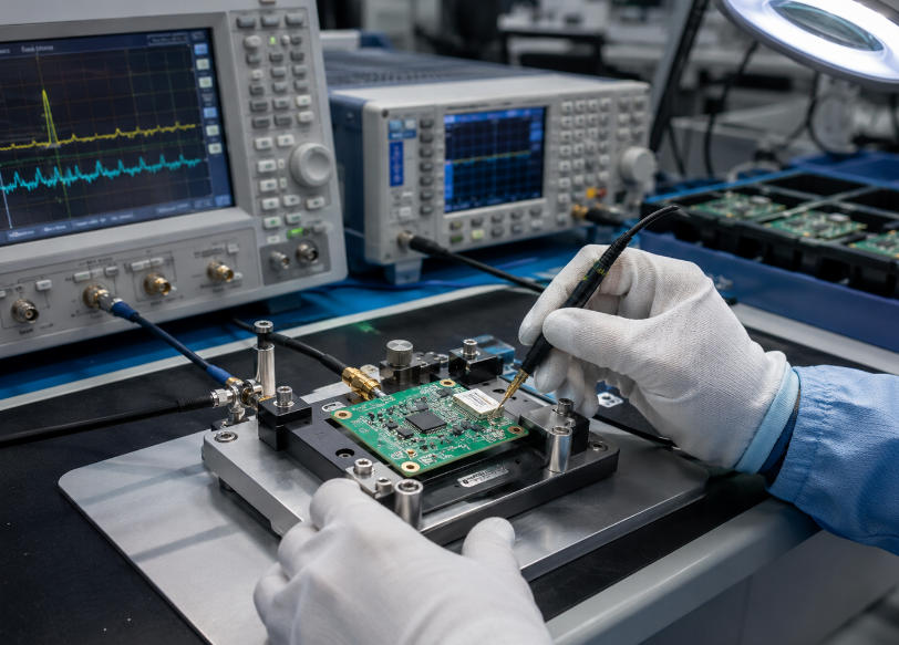
    Q7: Why should custom PCB assembly for access control systems include functional testing?

    A7: Functional testing confirms that the assembled board can actually work in the access control system. Visual inspection alone cannot verify reader input, relay output, network communication, sensor response, firmware status, or lock control performance.

    How Can You Start an IoT Access Control PCB Project with EBest?

    To start an IoT access control PCB project with EBest, send your Gerber files, BOM, pick-and-place file, assembly drawing, and testing requirements. If your board includes PoE, Ethernet, RS485, RFID, biometric modules, relays, or lock output circuits, EBest can review the production details before manufacturing.

    EBest provides IoT access control PCB manufacturing and assembly, component sourcing, DFM review, and functional test support for smart entry systems. For high-quality custom production and reliable project coordination, contact EBest at sales@bestpcbs.com and send your project files for quotation and technical review.

    You may also like

    Automotive PCB Fabrication | 20-Year Engineering-Driven PCB Manufacturer

    June 2nd, 2026

    Automotive PCB fabrication is more than producing a circuit board for a vehicle. It is about building a reliable electrical foundation for control modules, lighting systems, sensors, power electronics, battery systems, and connected automotive devices where heat, vibration, current load, impedance stability, and long service life all matter. This article explains how automotive PCB projects should be approached from materials, certifications, manufacturing control, case experience, and supplier selection.

    EBest Circuit (Best Technology) provides automotive PCB fabrication with 20 years of engineering-driven manufacturing experience. We support PCB fabrication, DFM review, material selection, impedance control, surface finish control, testing reports, traceability, and PCBA assembly as an extended service when customers need a complete build. For automotive PCB projects, pls feel free to send Gerber files, stack-up, specifications, and testing requirements to sales@bestpcbs.com for engineering review.

    Automotive PCB Fabrication

    Automotive PCB Fabrication Services by EBest Circuit (Best Technology)

    Automotive PCB fabrication requires stable production, controlled materials, accurate stack-up, and reliable inspection. For automotive electronics, the board is not just a carrier for components; it directly affects electrical safety, thermal behavior, signal quality, and long-term reliability.

    EBest Circuit (Best Technology) supports automotive PCB fabrication for different vehicle electronic applications, including:

    • Automotive lighting PCBs
      Used in LED headlights, tail lights, daytime running lights, interior lighting, and signal lamps. These boards often need metal core, heavy copper, or high-thermal materials to manage heat.
    • Control module PCBs
      Used in body control modules, motor control units, sensor controllers, and power control boards. These projects often require multilayer FR4, impedance control, and stable copper thickness.
    • Battery and power electronics PCBs
      Used in battery management systems, charging units, power conversion, and high-current circuits. Heavy copper, high-Tg FR4, copper substrate, or ceramic PCB may be required depending on current and temperature.
    • Sensor and communication PCBs
      Used in radar support boards, camera modules, signal processing boards, and communication-related vehicle electronics. These boards often require controlled impedance, stable dielectric performance, and precise fabrication tolerance.
    • Rigid-flex automotive PCBs
      Used where space is limited and connector reduction is important. Rigid-flex structures help improve mechanical integration and reduce assembly complexity.

    Our automotive PCB fabrication service can support prototype builds, engineering validation, small-batch production, and volume manufacturing. When required, EBest Circuit (Best Technology) can also extend support to PCBA assembly, including SMT assembly, through-hole assembly, X-ray inspection, AOI, functional testing, and box-build support. The main focus remains PCB fabrication, while assembly is available as a project extension.
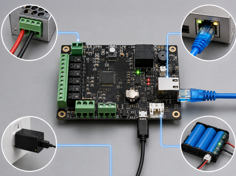
    Automotive PCB Fabrication

    PCB Material Solutions for Automotive Electronics

    Material selection is one of the first decisions in automotive PCB fabrication. The right board material helps the PCB handle heat, current, vibration, soldering cycles, and long operating time.

    EBest Circuit (Best Technology) helps customers choose PCB materials based on the actual electrical, mechanical, and thermal requirements of the automotive product.

    Common material options include:

    • High-Tg FR4 PCB
      High-Tg FR4 is suitable for multilayer automotive control boards, BMS boards, sensor boards, and power management circuits. It provides better thermal stability than standard FR4 and is often selected for products exposed to higher operating temperatures.
    • Heavy copper PCB
      Heavy copper is used for high-current automotive circuits, power conversion boards, relay control boards, and battery-related electronics. It improves current-carrying capacity and supports better heat spreading.
    • Metal core PCB
      Aluminum PCB and copper substrate PCB are widely used in automotive LED lighting and heat-dissipation applications. These boards help move heat away from power components and LED chips.
    • Ceramic PCB
      Ceramic PCB is used where high thermal conductivity, dimensional stability, and electrical insulation are important. It can be considered for high-power modules, LED systems, sensors, and advanced automotive electronics.
    • AMB ceramic PCB
      AMB ceramic PCB is suitable for high-power automotive applications such as power modules, IGBT modules, SiC devices, MOSFET circuits, and EV-related power electronics. It offers strong bonding and excellent heat transfer performance.
    • Rigid-flex PCB
      Rigid-flex boards are useful for compact automotive systems, camera modules, sensors, lighting assemblies, and space-limited electronic units. They can reduce connectors and improve mechanical reliability.
    • HDI PCB
      HDI PCB is suitable for dense automotive electronics that require fine lines, microvias, and compact routing. It is often used in modules where board space is limited but circuit density is high.

    A simple material selection view:

    PCB MaterialTypical Automotive Use
    High-Tg FR4Control modules, BMS, sensors
    Heavy CopperHigh-current and power circuits
    Aluminum PCBLED lighting and thermal boards
    Copper Substrate PCBHigh-power heat dissipation
    Ceramic PCBHigh-thermal and stable circuits
    AMB Ceramic PCBEV power modules and power devices
    Rigid-Flex PCBCompact automotive modules
    HDI PCBDense signal and control boards

    For automotive PCB fabrication, EBest Circuit (Best Technology) does not recommend materials only by name. We review the stack-up, copper weight, thermal load, dielectric requirement, soldering process, and end-use environment before suggesting the most suitable material direction.

    Automotive PCB Certifications and Compliance Support

    Automotive PCB customers usually care about more than price and lead time. They also need production consistency, documentation, traceability, and compliance support. This is especially important when the PCB will be used in vehicle lighting, control systems, power electronics, or regulated electronic modules.
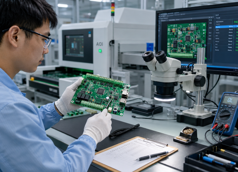
    EBest Circuit (Best Technology) supports automotive PCB projects with quality systems and documentation practices that help customers manage project risk.

    Key compliance and quality support may include:

    • IATF16949 support
      Important for automotive-related production management, process control, and continuous improvement.
    • ISO9001 quality management
      Supports stable manufacturing processes, documented procedures, and consistent product quality.
    • ISO13485 support
      Useful when customers also need medical-grade documentation discipline or cross-industry reliability control.
    • AS9100D support
      Relevant for high-reliability projects that need strong traceability and controlled production management.
    • UL support
      Important for material recognition, production flow control, and PCB safety-related requirements.
    • RoHS compliance
      Supports environmental compliance for electronic products sold into international markets.
    • IPC standard manufacturing
      Automotive PCB projects commonly reference IPC standards such as IPC-6012 for rigid PCB fabrication requirements and IPC-A-600 for board acceptance criteria.

    For documentation, automotive PCB buyers may request:

    • Certificate of Conformance
    • Electrical test report
    • Microsection report
    • Copper thickness report
    • Impedance test report
    • Solderability test report
    • Material compliance document
    • First Article Inspection report when needed
    • Production traceability record
    • Packaging and shipment inspection record

    For automotive PCB fabrication, documentation should not be treated as an afterthought. EBest Circuit (Best Technology) can provide controlled production records and inspection reports based on the customer’s project requirements, helping engineering and purchasing teams verify that the boards match the approved specification.

    Automotive PCB Fabrication Case Studies

    A real automotive PCB fabrication case is often more useful than a long capability list. It shows how the manufacturer controls material, impedance, documentation, and final testing in an actual automotive electronics project.

    The following case is based on a multilayer automotive control PCB. The customer background is generalized, while the key board requirements are kept to show the manufacturing focus.

    Project Overview

    • The project required a 12-layer FR4 PCB for an automotive electronic control application. The board used high-Tg ISOLA 408HR material and needed controlled impedance, ENIG surface finish, RoHS-compliant material, and complete outgoing quality reports.
    • For this automotive PCB fabrication project, the customer cared most about stable stack-up, electrical performance, production discipline, and shipment verification.

    Customer Requirements

    The main requirements included:

    • 12-layer FR4 multi-layer PCB
    • ISOLA 408HR High-Tg 170 material
    • Single-ended and differential impedance control
    • ENIG surface finish with controlled nickel and gold thickness
    • IPC-6012 Class 2 fabrication standard
    • RoHS-compliant PCB material
    • UL-compliant production flow
    • 100% continuity test before shipment
    • COC, microsection, E-test, solderability, copper thickness, and impedance reports

    Manufacturing Focus

    This automotive PCB fabrication case required careful control in several key areas:

    • Material and stack-up control
      The 12-layer structure needed stable lamination, controlled dielectric thickness, and verified high-Tg material selection.
    • Impedance control
      The board included both single-ended and differential impedance. Trace geometry, dielectric thickness, and copper thickness had to stay within the approved tolerance.
    • Surface finish control
      ENIG thickness was controlled to support solderability, surface stability, and assembly reliability.
    • Fabrication note control
      The project did not allow additional copper stealing. All unspecified holes followed N.C. drill data, and all slots were plated unless clearly marked as unplated.
    • Final verification
      Each board required 100% continuity testing before shipment, with outgoing reports prepared for customer review.

    EBest Circuit (Best Technology)’s Support

    EBest Circuit (Best Technology) reviewed the Gerber files, stack-up, fabrication notes, impedance requirements, and report requirements before production.

    Our engineering and production team supported the project through:

    • DFM review before fabrication
    • Material and stack-up confirmation
    • Controlled impedance manufacturing
    • ENIG thickness control
    • Drill and slot requirement review
    • 100% electrical continuity testing
    • Outgoing quality report preparation
    • Shipment inspection and traceability control

    Project Result

    • The automotive PCB fabrication project was completed with controlled material, impedance, surface finish, and final testing. The customer received boards with the required outgoing reports, helping their engineering team move forward with internal validation.

    Case Board Specifications

    ItemKey Specification
    Board Type12-layer FR4 multilayer PCB
    Board Thickness2.3 mm ±10%
    MaterialISOLA 408HR High-Tg 170
    Electrical PerformanceDk max. 3.7 @ 2GHz, Df max. 0.01 @ 10GHz
    Copper Thickness1 oz on selected layers, 0.5 oz on other layers
    Surface FinishENIG with controlled nickel and gold thickness
    Impedance ControlSingle-ended and differential impedance, ±10% tolerance
    ComplianceRoHS material, UL production flow
    Fabrication StandardIPC-6012 Class 2
    Testing100% continuity test before shipment
    Outgoing ReportsCOC, microsection, E-test, solderability, copper thickness, and impedance reports

    This case shows how EBest Circuit (Best Technology) supports automotive PCB fabrication projects that require more than basic board production. For automotive electronics, the value is not only making the PCB, but controlling the material, process, testing, and documentation behind it.

    How EBest Circuit (Best Technology) Supports Automotive PCB Projects from Prototype to Production

    Automotive PCB projects usually move through several stages before stable production. A good PCB fabrication supplier should support the customer from early design review to production delivery, not only quote the board after the files are finished.

    EBest Circuit (Best Technology) supports automotive PCB customers through each project stage.

    1. Design and DFM Review

    Before production, our engineering team reviews key PCB fabrication details:

    • Layer stack-up
    • Copper weight
    • Minimum trace and spacing
    • Drill size and aspect ratio
    • Annular ring
    • Controlled impedance
    • Material selection
    • Surface finish
    • Slot and routing requirements
    • Warpage risk
    • Panelization
    • Test point and inspection requirements

    This helps reduce manufacturing risk before the board enters production.

    2. Prototype Fabrication

    Prototype fabrication helps customers verify electrical design, mechanical fit, thermal performance, and assembly compatibility.

    For automotive PCB prototypes, common review points include:

    • Whether the selected material can support the operating temperature
    • Whether the copper weight matches the current requirement
    • Whether impedance can be held within tolerance
    • Whether the solder mask, finish, and hole design match assembly needs
    • Whether the board structure can be scaled to small-batch or volume production

    3. Small-Batch Validation

    Small-batch production is useful before mass production. It gives the customer a practical view of process stability, yield, and test performance.

    EBest Circuit (Best Technology) can support small-batch automotive PCB fabrication for:

    • Engineering validation
    • Pilot production
    • Pre-production builds
    • Customer sample approval
    • Assembly trial runs
    • Reliability test preparation

    4. Volume Manufacturing

    When the project moves into volume production, process consistency becomes more important than speed alone.

    Key production controls include:

    • Confirmed material source
    • Stable stack-up
    • Controlled lamination
    • Copper thickness verification
    • Impedance testing
    • Electrical testing
    • Lot traceability
    • Outgoing quality reports
    • Packaging and shipment control

    5. Optional PCBA Extension

    Some automotive customers need more than bare PCB fabrication. In that case, EBest Circuit (Best Technology) can also support PCBA assembly for FR4 PCB, high-Tg PCB, metal core PCB, rigid-flex PCB, heavy copper PCB, ceramic PCB, and HDI PCB projects.

    PCBA support may include:

    • SMT assembly
    • Through-hole assembly
    • Component sourcing
    • AOI inspection
    • X-ray inspection
    • Functional testing
    • Conformal coating when required
    • Box-build assembly for selected projects

    The core value remains clear: customers can start with automotive PCB fabrication and extend to assembly and testing when the project requires a more complete manufacturing route.

    Quality Control for Automotive PCB Fabrication

    Quality control in automotive PCB fabrication must be built into the process, not only checked at the end. A board may look acceptable visually but still fail because of impedance drift, weak solderability, insufficient copper thickness, plating issues, or hidden manufacturing defects.

    EBest Circuit (Best Technology) applies quality control across the full PCB manufacturing process.

    Important quality control points include:

    • Incoming material inspection
      PCB laminate, copper foil, solder mask, and process materials are checked according to project requirements.
    • DFM and engineering review
      Manufacturing risks are reviewed before production, especially for multilayer boards, controlled impedance boards, heavy copper boards, and special material boards.
    • Inner layer inspection
      Inner layers are checked before lamination to reduce the risk of hidden defects in multilayer PCBs.
    • Lamination control
      Lamination parameters are controlled to maintain board thickness, dielectric structure, and layer alignment.
    • Drilling and plating control
      Hole quality, copper plating, via reliability, and slot requirements are monitored during fabrication.
    • Impedance control
      Controlled impedance coupons or test methods are used when required by the customer specification.
    • Solder mask and surface finish inspection
      Solder mask coverage, legend quality, ENIG thickness, HASL, OSP, or other finishes are inspected based on the approved requirement.
    • Electrical testing
      100% electrical testing can be performed to check open and short circuits before shipment.
    • Final inspection and reporting
      Outgoing quality control verifies appearance, dimensions, reports, packing, and customer-specific requirements.

    Common inspection and test methods include:

    Quality ItemPurpose
    AOIChecks circuit pattern defects
    Electrical TestConfirms continuity and isolation
    MicrosectionVerifies plating and internal structure
    Impedance TestConfirms signal control
    Copper Thickness TestChecks copper build-up
    Solderability TestConfirms surface finish performance
    Visual InspectionChecks appearance and workmanship
    Final QCConfirms shipment readiness

    EBest Circuit (Best Technology) also uses MES traceability to support production tracking. This helps customers trace key production information, batch status, process flow, and inspection records more efficiently. For automotive PCB fabrication, this type of traceability is important because buyers need confidence not only in one shipment, but also in repeat production consistency.

    Why Choose EBest Circuit (Best Technology) for Automotive PCB Fabrication?

    Choosing an automotive PCB fabrication supplier is not only about finding a board factory. The better question is whether the supplier can understand the project requirement, prevent avoidable manufacturing problems, and support the customer from engineering review to stable delivery.

    EBest Circuit (Best Technology) is suitable for automotive PCB customers who need more than a basic PCB quotation.

    Key reasons to work with us include:

    • 20 years of PCB manufacturing experience
      We have long-term experience with PCB fabrication for industrial, automotive, medical, communication, lighting, power, and high-reliability electronics.
    • Engineering-driven project support
      Our team can review Gerber files, stack-up, materials, impedance requirements, copper thickness, fabrication notes, and assembly needs before production.
    • Wide PCB material capability
      We support FR4, high-Tg FR4, heavy copper, aluminum PCB, copper substrate PCB, ceramic PCB, AMB ceramic PCB, rigid-flex PCB, HDI PCB, and high-frequency PCB projects.
    • Automotive-related quality system support
      We can support automotive PCB projects with IATF16949, ISO9001, UL, and related quality documentation requirements.
    • DFM support before production
      DFM review helps customers avoid problems related to hole design, spacing, stack-up, impedance, solder mask, edge clearance, panelization, and manufacturability.
    • Controlled testing and reporting
      We can provide electrical test reports, microsection reports, impedance reports, copper thickness reports, solderability reports, COC, and other outgoing documents based on customer requirements.
    • MES traceability
      Production traceability helps customers track manufacturing status and batch information more clearly.
    • Prototype to production capability
      We support engineering samples, small-batch production, and mass production, helping customers move through the project lifecycle with one manufacturing partner.
    • Optional PCBA assembly support
      When customers need assembly after bare board fabrication, we can support component sourcing, SMT assembly, through-hole assembly, AOI, X-ray, functional testing, and box-build service.

    For automotive PCB fabrication, EBest Circuit (Best Technology) combines board manufacturing, engineering review, quality control, reporting, and delivery support. Customers who need a reliable PCB partner can send project files and requirements to sales@bestpcbs.com for review.
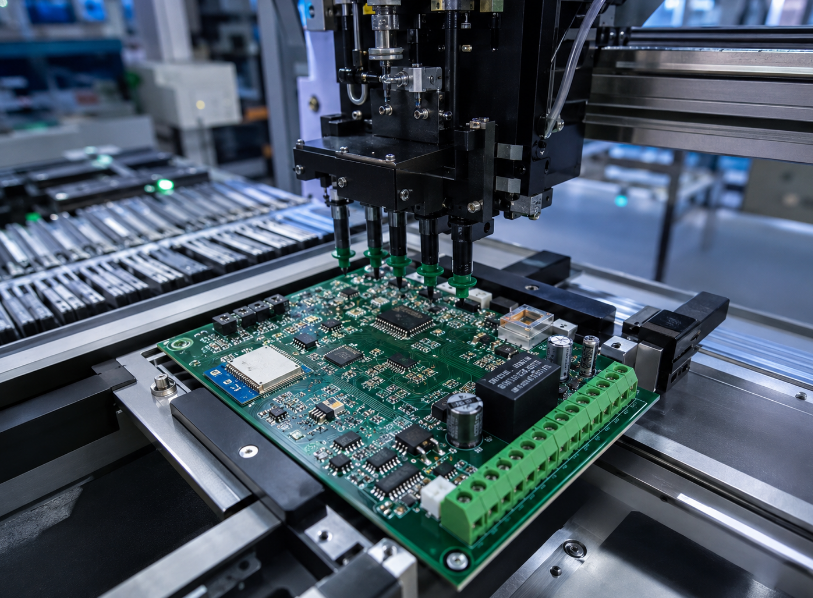
    Automotive PCB Fabrication

    FAQs About Automotive PCB Fabrication

    What is automotive PCB fabrication?

    • Automotive PCB fabrication is the manufacturing process for printed circuit boards used in vehicle electronic systems. These boards may be used in lighting, power control, sensors, battery systems, control modules, radar support circuits, and other automotive electronics.

    How is automotive PCB fabrication different from standard PCB fabrication?

    • Automotive PCB fabrication usually requires stronger control over materials, heat resistance, copper thickness, dimensional tolerance, impedance, testing, documentation, and traceability. The board must support stable performance in demanding vehicle environments.

    What materials are commonly used for automotive PCB fabrication?

    • Common materials include high-Tg FR4, heavy copper, aluminum substrate, copper substrate, ceramic, AMB ceramic, rigid-flex materials, and HDI structures. The right choice depends on thermal load, current, signal speed, space, and reliability requirements.

    Is High-Tg FR4 suitable for automotive PCBs?

    • Yes. High-Tg FR4 is commonly used for automotive control boards, BMS boards, sensor boards, and multilayer electronics where better thermal stability is required. It is often a practical choice when the project does not require metal core or ceramic material.

    When should metal core PCB be used in automotive electronics?

    • Metal core PCB is suitable when heat dissipation is a major concern. It is commonly used in automotive LED lighting, power LED modules, and some high-thermal control applications.

    When is ceramic PCB used in automotive PCB fabrication?

    • Ceramic PCB is used when high thermal conductivity, stable insulation, and dimensional stability are important. It may be selected for power modules, LED systems, sensors, and advanced automotive electronics.

    What is AMB ceramic PCB used for in automotive applications?

    • AMB ceramic PCB is often used in high-power applications such as EV power modules, IGBT modules, SiC devices, MOSFET circuits, and other power electronics that require strong thermal performance and reliable copper bonding.

    Do automotive PCBs require controlled impedance?

    • Many automotive PCBs require controlled impedance, especially boards used for communication, sensors, signal processing, radar support, and high-speed control circuits. The impedance tolerance should be confirmed during stack-up design and fabrication review.

    What documents can be provided for automotive PCB fabrication?

    • Depending on the project requirement, EBest Circuit (Best Technology) can provide COC, electrical test report, microsection report, solderability report, copper thickness report, impedance report, material compliance document, and other outgoing quality records.

    Can EBest Circuit (Best Technology) support automotive PCB assembly after fabrication?

    • Yes. Although automotive PCB fabrication is the main focus, we can also support PCBA assembly when customers need a complete manufacturing solution. This may include component sourcing, SMT assembly, through-hole assembly, AOI, X-ray inspection, functional testing, and box-build support.
    How do I choose an automotive PCB fabrication manufacturer?

    • Look for a supplier with automotive project experience, material selection capability, DFM support, controlled testing, quality documentation, traceability, and stable production capacity. Price is important, but engineering support and repeatable quality are more important for automotive electronics.

    How can I request a quotation for automotive PCB fabrication?

    • You can send Gerber files, stack-up, BOM, assembly drawing, material requirements, impedance requirements, testing requirements, and expected quantity to sales@bestpcbs.com. EBest Circuit (Best Technology) will review the files and provide feedback for your automotive PCB fabrication project.

    You may also like

    Certified Medical Electronics PCB Supplier with DFM Support

    June 2nd, 2026

    Medical electronics PCB supplier selection affects the reliability, manufacturability, documentation, and long-term stability of medical device electronics. This blog explains how to evaluate a qualified PCB supplier for medical projects, what PCB manufacturing capabilities matter, and why DFM support should be checked before prototype or batch production.

    As a medical electronics PCB supplier, EBest Circuit (Best Technology) supports medical PCB fabrication, PCBA assembly, component sourcing, DFM review, testing, and traceability-focused production. Our engineering team helps customers review PCB structure, materials, panelization, assembly risks, and documentation needs before manufacturing. For a professional project review, please send your Gerber files, BOM, and requirements to sales@bestpcbs.com.

    Medical Electronics PCB Supplier

    Top 10 Medical Electronics PCB Suppliers in China

    The following list is for supplier reference, not an official ranking. Each company has its own market focus, so buyers should compare PCB fabrication capability, DFM support, PCBA experience, quality control, testing, traceability, and communication efficiency before choosing a medical electronics PCB supplier.

    No.CompanyCompany Positioning
    1EBest Circuit (Best Technology)Engineer-oriented one-stop PCBA service provider
    2Venture ElectronicsDesign-to-turnkey PCB solution provider
    3Grandtop GroupCustomized medical PCBA manufacturer
    4ChinaPCBACompliance-focused medical PCB assembly supplier
    5GNS PCBAMedical-grade EMS manufacturing partner
    6JHYPCBQuick-turn PCB prototype and assembly supplier
    7ViasionLow-to-medium volume custom PCB manufacturer
    8Rich Full JoyPCB design and manufacturing integration provider
    9KKPCBShenzhen-based medical PCB prototyping supplier
    10WellPCBOnline one-stop PCB and PCBA service provider

    For medical electronics buyers, the best supplier is not always the largest factory. A stronger choice is often the supplier that can understand the PCB design, review manufacturability risks early, control production records, and support repeatable quality from prototype to batch production.

    Medical Electronics PCB Supplier

    Why Are Medical PCB Assemblies Critical in Modern Medical Devices?

    Medical PCB assemblies are critical because they carry the electronic functions inside medical devices. A PCB or PCBA may support sensing, power management, signal processing, communication, display control, battery charging, or safety-related monitoring.

    For customers, the key points are:

    • They affect device accuracy.
      In diagnostic and monitoring equipment, signal quality depends on PCB layout, grounding, routing, material choice, and assembly stability.
    • They support long-term reliability.
      Medical devices often need stable performance over repeated use. Solder joints, vias, copper layers, surface finish, and component quality all matter.
    • They influence production consistency.
      A medical PCB should be designed and manufactured for repeatable production, not only one successful prototype build.
    • They require stronger documentation.
      Medical customers may need COC, inspection records, test data, material information, and production traceability.
    • They connect design quality with real manufacturing.
      A good design still needs correct stack-up, copper balance, panelization, solderability, and inspection planning.

    In short, medical PCB assemblies are not ordinary circuit boards. They are controlled electronic modules that need engineering review, stable PCB manufacturing, reliable assembly, quality inspection, and traceability.

    Why Is DFM Important for Medical PCB Assemblies?

    DFM, or Design for Manufacturing, helps find manufacturing risks before the PCB enters fabrication or assembly. For medical PCB assemblies, this step is valuable because late design changes can delay validation, increase cost, and affect delivery plans.

    The main value of DFM is simple:

    • Find risks before production starts.
    • Improve PCB manufacturability.
    • Reduce assembly defects.
    • Improve yield and consistency.
    • Support smoother prototype-to-production transfer.
    • Help customers avoid unnecessary manufacturing cost.

    For medical PCB projects, a useful DFM review should check:

    • Trace width and spacing.
    • Via size and annular ring.
    • Layer stack-up and copper balance.
    • Board thickness and warpage risk.
    • Solder mask clearance.
    • Pad design for fine-pitch components.
    • BGA and IC assembly risk.
    • Fiducial marks and tooling holes.
    • Panelization and process edge design.
    • Test point accessibility.
    • Surface finish suitability.
    • Component spacing and polarity marking.

    For example, if a medical PCB uses fine-pitch ICs or BGA packages, pad design and solder paste control become very important. If the panel lacks proper fiducial marks, SMT placement accuracy may be affected. If the copper balance is poor, the board may have higher warpage risk during reflow.

    That is why a medical device PCB assembly manufacturer should not only quote the board. It should also review the files and give practical engineering feedback before production.

    What Specialized PCB Technologies Are Used in Medical Applications?

    Different medical devices need different PCB technologies. A reliable medical electronics PCB supplier should recommend the board structure based on application, signal requirement, thermal load, size limit, reliability target, and assembly complexity.

    Common PCB technologies used in medical electronics include:

    • Multilayer FR4 PCB
      • Used in control boards, diagnostic equipment, monitoring systems, and communication modules.
      • Supports compact routing, stable power planes, and better signal separation.
    • High-Tg FR4 PCB
      • Suitable for medical boards that need better thermal stability.
      • Tg170 FR4 is often selected for multilayer boards that go through SMT reflow and long-term operation.
    • HDI PCB
      • Used in compact medical devices, handheld instruments, wearable electronics, and dense BGA layouts.
      • Supports microvias, fine lines, and higher routing density.
    • Flexible PCB
      • Used in wearable sensors, portable medical products, and lightweight electronic modules.
      • Helps reduce space and improve mechanical flexibility.
    • Rigid-Flex PCB
      • Used when the product has limited internal space or moving sections.
      • Reduces connectors and cable assembly, which can improve internal reliability.
    • Metal Core PCB
      • Used in medical lighting, power modules, and thermal management applications.
      • Helps transfer heat away from power components or LEDs.
    • Ceramic PCB
      • Used in high-power, high-thermal, laser-related, or special sensor applications.
      • Offers excellent thermal conductivity and dimensional stability.
    • High-Frequency PCB
      • Used in wireless medical devices, RF modules, antenna boards, and communication-related medical equipment.
      • Helps control signal loss and impedance stability.
    • ENIG Surface Finish
      • Common in medical PCB assemblies with fine-pitch components or BGA packages.
      • Provides a flat pad surface and stable solderability.

    The right technology is not always the most expensive one. The best choice is the PCB structure that matches the device’s electrical, mechanical, thermal, and quality requirements.

    As a medical electronics PCB supplier, EBest Circuit (Best Technology) supports a wide range of medical circuit board technologies, including multilayer boards, High-Tg FR4 boards, HDI circuits, flexible circuits, rigid-flex boards, metal-based boards, ceramic substrates, RF circuit boards, and ENIG-finished PCBs. Our engineering team helps customers select the right board structure based on thermal demand, signal performance, assembly complexity, and production reliability. This allows medical electronics projects to move from design review to stable manufacturing with better technical control.

    What Certifications Should a Medical Device PCB Assembly Manufacturer Have?

    A medical device PCB assembly manufacturer should have a quality system that supports controlled production, traceability, documentation, and stable process management. For medical electronics, certifications are useful because they show whether the supplier has a structured way to manage quality, production records, and customer requirements.

    A buyer should not only ask, “Do you have certificates?”
    A better question is, “How do you apply these standards during real production?”

    Certification / StandardWhat Buyers Should Check
    ISO 13485Medical quality system and documentation control
    ISO 9001General quality management foundation
    IPC-A-610Assembly workmanship acceptance standard
    IPC Class 2 / Class 3Required reliability level for the product
    ULMaterial or product safety recognition when required
    RoHS / REACHEnvironmental compliance for restricted substances
    IATF 16949Useful for automotive-grade quality systems
    AS9100DUseful for aerospace or high-reliability projects

    For medical PCB assemblies, certifications are only part of the evaluation. The supplier should also show:

    • Clear incoming material control.
    • Stable PCB fabrication process control.
    • SMT process control.
    • AOI and X-ray inspection capability.
    • Functional testing support when needed.
    • Batch traceability.
    • Documented quality records.
    • Engineering communication before production.

    A certificate gives confidence. A controlled process gives real reliability. EBest Circuit (Best Technology) supports medical PCB and PCBA projects with ISO 13485, ISO 9001, IATF 16949, and AS9100D certified quality systems, along with UL recognition, RoHS, and REACH compliance support. Beyond certificates, our focus is controlled material sourcing, stable PCB fabrication, SMT inspection, testing support, traceability, and complete shipment records.
    How Does a Medical PCB Manufacturer Control Quality and Traceability?

    A medical PCB manufacturer should control quality from engineering review to final shipment. The process should be layered, not dependent on one final inspection.

    Engineering Review

    • Check Gerber, drill, BOM, pick-and-place, assembly drawing, and special notes.
    • Review stack-up, copper thickness, board thickness, surface finish, and panel design.
    • Confirm DFM issues before fabrication and assembly.

    Material Control

    • Verify base material, copper foil, solder mask, surface finish, and components.
    • Check approved sources for critical parts.
    • Confirm substitutions with the customer before use.
    • Keep batch and lot information when required.

    PCB Fabrication Control

    • Inspect inner layers before lamination.
    • Control drilling, plating, imaging, etching, solder mask, and surface finish.
    • Use electrical testing to check open and short circuits.
    • Check dimensions, appearance, and finished thickness.

    SMT Assembly Control

    • Control solder paste printing.
    • Use SPI to inspect solder paste volume and alignment.
    • Use AOI to check placement, polarity, solder joints, and missing parts.
    • Use X-ray for BGA, QFN, and hidden solder joints when needed.
    • Control reflow profile according to board and component requirements.

    Testing Control

    • Support flying probe, ICT, functional testing, or custom test fixtures when required.
    • Confirm test method before production.
    • Record test results for quality review.

    Traceability Control

    • Link finished boards to material batches, production records, inspection data, and shipment information.
    • Keep records available for repeat orders, quality audits, and failure analysis.
    • Provide documents such as COC, inspection reports, or test records when required.

    For medical electronics, traceability is not just paperwork. It helps customers understand what was built, when it was built, which materials were used, and how the product was inspected.

    At EBest Circuit (Best Technology), quality and traceability are supported by our ISO 13485 quality management system and MES-based production tracking. From material receiving, PCB fabrication, SMT assembly, inspection, testing, to final shipment, key production data can be recorded and traced through the manufacturing process. This helps medical electronics customers gain clearer control over batch records, process status, inspection results, and shipment documentation, making each medical PCB project more transparent and reliable.

    What Types of Medical PCB Assemblies Can Be Manufactured?

    Medical PCB assemblies can be simple, compact, high-density, power-related, signal-sensitive, or thermally demanding. The supplier should match the board type to the actual device requirement.

    Common medical PCB assembly types include:

    • Medical Control Board Assembly
      • Used in equipment control systems, operation panels, and embedded control modules.
    • Sensor PCB Assembly
      • Used in monitoring devices, diagnostic instruments, and signal acquisition modules.
    • Power Management PCBA
      • Used in battery charging, power conversion, protection circuits, and portable medical devices.
    • Display and Interface PCBA
      • Used in screens, keypads, control panels, and user operation modules.
    • Communication PCB Assembly
      • Used in Bluetooth, Wi-Fi, RF, and data transmission modules for connected medical devices.
    • Wearable Medical PCBA
      • Used in health monitoring devices, portable sensors, and compact patient-care electronics.
    • Diagnostic Equipment PCBA
      • Used in analyzers, laboratory instruments, measurement systems, and test equipment.
    • Imaging-Related PCBA
      • Used in signal processing, power control, and communication boards for imaging systems.
    • Medical Lighting PCBA
      • Used in LED light source boards, control boards, and thermal management modules.
    • Rigid-Flex Medical PCBA
      • Used in compact devices where flexible interconnection can reduce connectors and save space.

    The best solution depends on board size, component density, operating environment, signal type, production volume, and testing requirements.

    EBest Circuit (Best Technology) supports a wide range of medical PCB and PCBA projects, including multilayer FR4 boards, rigid-flex PCBs, HDI boards, sensor PCB assemblies, control boards, power management PCBAs, and communication-related medical electronics. With PCB fabrication, component sourcing, PCBA assembly, DFM review, testing, and traceability support under one workflow, we help customers move from prototype verification to stable production with fewer manufacturing risks.

    Case Study: How EBest Circuit (Best Technology) Supports a Medical Electronics PCB Project

    This case is based on an 8-layer FR4 PCB used in a medical electronics project. To protect customer confidentiality, the device details are described in a general way. The board was designed for a compact medical electronic module that required stable multilayer PCB manufacturing, multilayer PCB assembly, good solderability, controlled panelization, and shipment documentation.

    Project Overview

    • The customer needed a thin 8-layer medical PCB with Tg170 FR4 material, ENIG surface finish, and 1.0mm ±10% finished thickness. The board had limited layout space, so the stack-up, copper balance, surface finish, and panel design all needed careful review before production.

    Customer Requirements

    The main requirements included:

    • 8-layer FR4 PCB structure.
    • Tg170 high-Tg material.
    • 1.0mm ±10% finished thickness.
    • 0.5oz inner copper and 1oz outer copper.
    • ENIG surface finish with Au 2u”.
    • Green solder mask and white silkscreen.
    • Maximum panel size of 45 × 40cm.
    • Process edges and fiducial marks for production.
    • Electronic COC provided with shipment.

    Manufacturing Focus

    This project required attention to several key points:

    • Stack-up control: The 8-layer structure had to meet the 1.0mm thickness requirement.
    • Thermal stability: Tg170 FR4 helped improve dimensional stability during fabrication and later assembly.
    • Copper balance: 0.5oz inner copper and 1oz outer copper supported both routing and soldering reliability.
    • Solderability: ENIG with Au 2u” provided a flat surface for fine-pitch assembly.
    • Panelization: Process edges and fiducial marks helped support accurate SMT handling.
    • Documentation: Electronic COC supported the customer’s internal quality records.

    EBest Circuit’s Support

    • EBest Circuit reviewed the project from both PCB manufacturing and assembly-readiness perspectives. Our engineering team checked the stack-up, copper balance, material selection, ENIG requirement, panel design, fiducial mark placement, and shipment documentation before production.

    Project Result

    • The PCB was manufactured according to the customer’s technical requirements and delivered with the required electronic COC. The project showed how a medical electronics PCB supplier can help reduce manufacturing risk through early engineering review, controlled fabrication, panelization support, and documentation readiness.

    Case Board Specifications

    ItemSpecification
    ApplicationMedical electronics PCB project
    PCB TypeMultilayer FR4 PCB
    Layer Count8 layers
    Base MaterialFR4
    Tg ValueTg170
    Inner Copper Thickness0.5oz
    Outer Copper Thickness1oz
    Finished Board Thickness1.0mm ±10%
    Surface FinishENIG
    Gold ThicknessAu 2u”
    Solder MaskGreen
    SilkscreenWhite
    Maximum Panel Size45 × 40cm
    Panel RequirementProcess edge included with fiducial mark points
    Shipment DocumentElectronic COC provided

    How to Get a Quote from a Medical Electronics PCB Supplier?

    To get an accurate quote from a medical electronics PCB supplier, customers should provide complete manufacturing and assembly information. A medical PCB quote is not only based on board size and quantity. It also depends on material, layer count, copper thickness, surface finish, tolerance, test requirements, component availability, assembly complexity, and documentation needs.

    For bare PCB fabrication, the basic files and information should include:

    • Gerber files
    • Drill files
    • Stack-up requirement
    • Board thickness
    • Copper thickness
    • Surface finish
    • Solder mask color
    • Silkscreen color
    • Material requirement
    • Impedance requirement, if any
    • Finished copper or hole wall requirement, if any
    • Panelization requirement
    • Quantity and delivery schedule
    • Required certificates or reports
    Medical Electronics PCB Supplier

    For PCBA quotation, the customer should also provide:

    • BOM with manufacturer part numbers
    • Pick-and-place file
    • Assembly drawing
    • Testing method
    • Programming requirement, if any
    • Functional test instructions, if any
    • Special soldering or cleaning requirement
    • Conformal coating requirement, if any
    • Packaging requirement
    • Approved vendor list, if required
    • Substitute component rules

    For medical projects, it is also helpful to share the end-use category. The supplier does not always need confidential product details, but basic application information helps engineering teams understand the reliability level. For example, a board used in a laboratory instrument may have different requirements from a wearable device, medical lighting board, or diagnostic control module.

    Customers should also state documentation needs at the quotation stage. If the project requires COC, RoHS report, material declaration, first article inspection, test report, production photos, or traceability records, these should be confirmed before production. This avoids confusion near shipment.

    When you request a quote from EBest Circuit (Best Technology), our team will not only calculate the PCB or PCBA cost. We will also review your Gerber files, BOM, stack-up, material requirements, panelization, test needs, and any potential manufacturing risks before production. This helps customers receive a more accurate quotation and practical engineering feedback at the same time. If you are working on a medical PCB or medical PCBA project, please send your files and requirements to sales@bestpcbs.com. Our engineering team will review your project and support you from quotation to manufacturing.

    FAQs About Choosing a Medical Electronics PCB Supplier

    What is a medical electronics PCB supplier?
    A medical electronics PCB supplier provides PCB fabrication, PCBA assembly, component sourcing, testing, documentation, and manufacturing support for medical electronics projects.

    Is a medical electronics PCB supplier different from a normal PCB factory?
    Yes. A normal PCB factory may only focus on board fabrication. A medical electronics PCB supplier should also support DFM review, process control, inspection, traceability, and medical-grade documentation.

    What files are needed for medical PCB assemblies?
    For PCB fabrication, Gerber files, drill files, stack-up, and specifications are needed. For PCBA, the supplier also needs BOM, pick-and-place file, assembly drawing, and testing instructions.

    Is ISO 13485 required for medical PCB assembly?
    It depends on the product and customer requirement. However, ISO 13485 is highly relevant for medical device supply chains because it focuses on medical device quality management and documentation control.

    What surface finish is suitable for medical PCB assemblies?
    ENIG is commonly used because it provides good flatness and stable solderability. It is suitable for fine-pitch components, BGA packages, and many medical electronics boards.

    Why is traceability important in medical PCB manufacturing?
    Traceability connects the finished PCB or PCBA with material batches, production records, inspection data, and shipment documents. This helps with audits, repeat orders, and quality review.

    Can medical PCBs use standard FR4 material?
    Yes. Many medical PCBs use FR4. For higher thermal stability, High-Tg FR4 such as Tg170 may be selected.

    What is the benefit of DFM for medical PCB assemblies?
    DFM helps find design and manufacturing risks before production. It can reduce delays, improve yield, and make the board easier to manufacture consistently.

    How should I compare medical electronics PCB suppliers?
    Compare PCB fabrication capability, engineering support, certification status, PCBA experience, component sourcing, inspection process, testing support, documentation ability, and traceability system.

    What should I provide when requesting a quote?
    Please provide Gerber files, BOM, pick-and-place file, assembly drawing, quantity, delivery requirement, test method, and documentation needs. For medical PCB or PCBA projects, you can send your files to sales@bestpcbs.com. Our engineering team will review the project and provide practical feedback before quotation.

    You may also like

    Top 10 Flexible Circuit Board Suppliers for Medical Devices

    May 29th, 2026

    Finding the right flexible circuit board suppliers for medical devices is not only about price. Medical electronics usually require compact design, stable quality, clean documentation, and reliable assembly support.
    Flexible circuits are used in wearable monitors, hearing aids, diagnostic tools, imaging systems, catheter systems, and portable medical devices. This guide helps you quickly compare board types, design points, manufacturing capabilities, certifications, and supplier options. For project review or medical PCB assembly quotes, you can also send your Gerber files and BOM to sales@bestpcbs.com.

    Flexible Circuit Board Suppliers for Medical Devices

    What Are Flexible Circuit Boards for Medical Devices?

    Flexible circuit boards are PCBs made with bendable materials, usually polyimide. They can fold, bend, or fit into small spaces where standard rigid PCBs are not practical.

    For medical devices, flexible circuits help reduce wiring, save space, and improve internal structure. They are often used to connect sensors, displays, batteries, buttons, antennas, and control modules.

    TypeTypical Use
    Single-sided flex circuitsSimple medical interconnection
    Double-sided flex circuitsMore routing space
    Multilayer flex circuitsHigher signal density
    Rigid flex circuit boardsCompact medical device structures
    Custom etched flex circuitsSensor and special connection designs

    Why Medical Flex Circuits Are Used in Medical Electronics?

    Medical flex circuits are used because medical products are becoming smaller, lighter, and more integrated.

    They help engineers:

    • Reduce cables and connectors
    • Save internal space
    • Improve assembly layout
    • Support curved or compact housings
    • Connect multiple functional areas
    • Build lightweight medical electronics

    In many medical devices, the circuit must fit the product shape. That is where flex circuits and rigid-flex boards become practical.

    What Types of Flexible Circuit Boards Are Used in Medical Devices?

    EBest Circuit (Best Technology) supports several flexible PCB types for medical electronics projects.

    Board TypeApplication Fit
    Single-sided flexible circuitsSimple signal connection
    Double-sided flexible circuitsMedium-density routing
    Multilayer flexible circuitsCompact medical modules
    Rigid flex circuit boardsIntegrated rigid + flexible structure
    Custom flexible PCBDevice-specific mechanical design
    Custom etched flex circuitsSensor, electrode, and special circuit paths
    Flexible PCB with stiffenerConnector or SMT support
    Medical PCB assembliesFabrication + component assembly

    These board types are suitable for wearable devices, portable diagnostic equipment, handheld instruments, monitoring devices, and compact medical control modules.

    Medical Device PCB Design: PCB Layout Guidelines for Flexible Circuits

    Medical device PCB design should start from the product structure, not only the schematic.

    Design AreaWhat to Check
    Bend radiusAvoid sharp bending in flex areas
    Trace routingUse smooth routing in bending zones
    Component placementKeep parts away from active flex areas
    ViasAvoid vias in repeated bending areas
    Stiffener locationSupport connectors and SMT areas
    GroundingImprove signal stability
    ShieldingProtect sensitive medical signals
    DFM reviewCheck manufacturability before production

    For rigid flex circuit boards, the transition area between rigid and flex sections is especially important. Poor layout in this area can affect yield and reliability.

    Custom Flexible PCB and Medical PCB Assembly Manufacturing Capabilities

    EBest Circuit (Best Technology) provides comprehensive end-to-end solutions, from custom flexible PCB​ fabrication and rigid flex circuit boards​ integration to precision medical device PCB assembly services. Our operations are engineered specifically to meet the stringent reliability, miniaturization, and regulatory demands of the healthcare industry.

    Core Capabilities in Medical-Grde Flex Circuits

    As experts in medical flex circuits, we utilize advanced custom etched flex circuits​ technology to ensure superior performance:

    • Material Mastery:​ We utilize medical-grade polyimide (PI) and LCP substrates, ensuring full compliance with ISO 13485 and RoHS standards.
    • Precision Fabrication:​ Our capabilities include fine-line trace routing and micro-via technology, perfect for the compact medical device PCB design​ required in modern implants and wearables.
    • Rigid-Flex Solutions:​ We seamlessly integrate flex circuits​ with rigid sections, providing 3D packaging solutions that reduce weight and improve signal integrity for critical medical electronics.

    Excellence in Medical PCB Assembly

    Being a trusted medical PCB manufacturer​ means we never compromise on quality. Our medical PCB assembly​ processes are designed for zero-defect outcomes:

    • Advanced Assembly:​ We offer high-precision SMT, BGA/CSP placement, and medical electronics assembly​ with sterilization-resistant coatings.
    • Quality Assurance:​ Our medical PCB assembly services​ include 100% AOI/X-ray inspection and functional testing, aligning with FDA and GMP requirements.
    • Full-System Integration:​ From prototype to volume production of medical PCB assemblies, we manage the entire lifecycle, including box-build integration.

    Ready to start your next medical electronic assembly project? Just feel free to contact EBest Circuit (Best Technology)​ at sales@bestpcbs.com​ for expert support with your custom flexible PCB​ and medical PCB assemblies.

    Certifications for Medical PCB Manufacturing and Assembly

    Certifications help customers screen medical PCB suppliers faster.

    Certification / StandardWhy It Matters
    ISO 9001General quality management
    ISO 13485Medical device quality management
    IPC standardsPCB fabrication and assembly workmanship
    RoHS / REACHMaterial compliance for global markets
    UL materialsRequired for some product designs

    For high-reliability medical electronics, IPC Class 3 is often discussed during flex PCB manufacturing review.

    Medical Applications Using Rigid Flex Circuit Boards

    Rigid flex circuit boards are used when a medical device needs both mechanical support and flexible connection.

    ApplicationWhy Rigid-Flex Helps
    Wearable monitorsThin, light, body-friendly structure
    Hearing aidsCompact curved internal layout
    EndoscopesNarrow and flexible circuit path
    Catheter systemsLong, thin, flexible connection
    Portable diagnostic toolsReduced cables and smaller housing
    Imaging equipmentStable signal routing
    Surgical instrumentsCompact and durable internal design
    Patient monitoring devicesIntegrated sensor and control connection

    Case Study: EBest Circuit (Best Technology) Manufacturing Medical Flex Circuits

    Project Type:
    2-layer medical FPC for compact medical electronics.

    Customer Requirement:
    The customer needed a thin, flexible circuit with steel stiffeners on both sides for better assembly support.
    EBest Circuit (Best Technology) Support:

    • Reviewed FPC stack-up and material structure
    • Checked coverlay opening and solder mask design
    • Controlled steel stiffener alignment
    • Used ENIG finish for stable solderability
    • Added white silkscreen markings for UL 94 V-0 and RoHS
    • Controlled bonding with 0.025mm pure thermal adhesive

    Manufacturing Focus:
    Thin FPC structure, stiffener bonding, flatness control, coverlay registration, and final surface quality.

    Board Parameters

    ItemSpecification
    Board Type2-layer FPC
    Board Thickness0.16mm ±0.03mm
    Copper Type1/2 oz ED Cu
    Base Material1 mil adhesive PI
    Coverlay1 mil yellow coverlay
    Surface FinishENIG 2U”
    Solder MaskGreen solder mask
    SilkscreenWhite silkscreen
    Compliance MarkingUL 94 V-0, RoHS
    Top Stiffener0.2mm steel stiffener
    Bottom Stiffener0.2mm steel stiffener
    Stiffener Adhesive0.025mm pure thermal adhesive
    Key Control PointsStiffener alignment, bonding strength, flatness, coverlay registration

    Top 10 Flexible Circuit Board Suppliers for Medical Devices

    Below are 10 suppliers commonly found when researching medical flex circuits, rigid-flex PCBs, and medical PCB assembly services.

    Company NameCertificationsKey Capabilities
    EBest Circuit (Best Technology)ISO 9001, ISO 13485, UL, RoHSMedical flex circuits, rigid-flex PCB, medical PCB assembly, DFM review
    Epec Engineered TechnologiesISO, UL, IPCMedical flex PCB, rigid-flex PCB, reliability testing
    FralockISO 13485, ISO 9001, AS9100D, FDA registeredFlex circuits, rigid-flex, stiffeners, shielding, turnkey builds
    BENCORISO 9001, ULFlexible PCB, rigid-flex PCB, design, fabrication, assembly
    Rush PCBISO 9001, ISO 13485, UL, RoHS/REACHFlex PCB, rigid-flex PCB, medical PCB assembly, quick-turn service
    All Flex SolutionsAS9100, ISO 9001, ESD S20.20Flexible circuits, CatheterFlex, rigid-flex, medical device PCBs
    MincoISO 9001, AS9100D, NadcapHigh-reliability flex circuits, rigid-flex, multilayer flex
    Cirexx InternationalISO 9001, AS9100, ITAR, IPCFlex PCB, rigid-flex PCB, layout, fabrication, assembly
    Flex Plus FPCISO 9001, ISO 13485, IATF 16949, ULMedical FPC, hearing aid FPC, portable monitor FPC
    HT Medical DevicesISO 13485, FDA registered product buildsFlexible circuits, rigid-flex, catheter flex, endoscope flex

    Before choosing a supplier, compare certifications, flex PCB capability, assembly support, traceability, quote speed, and engineering communication.

    How to Choose Flexible Circuit Board Suppliers for Medical Devices

    Use this checklist before sending a medical PCB project to a supplier:

    CheckpointWhy It Matters
    Medical PCB experienceReduces communication risk
    Flex and rigid-flex capabilitySupports more device structures
    ISO 13485Important for medical supply chains
    DFM supportFinds layout issues early
    SMT assemblySaves supplier coordination time
    Component sourcingSupports one-stop medical electronics assembly
    Testing capabilityImproves delivery confidence
    TraceabilityHelps audits and production records
    Fast RFQ responseSpeeds up project evaluation

    A strong supplier should not only quote. They should review your files and point out manufacturing risks.

    Future Trends of Custom Flexible PCB for Medical Devices

    Custom flexible PCB will continue to grow in medical electronics because devices are getting smaller and more wearable.

    Key trends include:

    • More wearable medical monitors
    • More rigid-flex designs in compact devices
    • Smaller sensor modules
    • Higher-density routing
    • Better signal shielding
    • Stronger traceability requirements
    • More demand for one-stop PCB + assembly service
    • Earlier DFM review before production

    For medical device developers, this means the PCB supplier should join the project earlier, not only after the design is finished.

    FAQs About Flexible Circuit Board Suppliers for Medical Devices

    Q1. What are flexible circuit board suppliers for medical devices?
    They are PCB manufacturers that provide flex circuits, rigid-flex boards, and sometimes medical PCB assembly for medical electronics.

    Q2. What are medical flex circuits used for?
    They are used in wearable monitors, hearing aids, diagnostic devices, imaging systems, catheter systems, and compact medical electronics.

    Q3. What is the difference between flex circuits and rigid flex circuit boards?
    Flex circuits are bendable boards. Rigid flex circuit boards combine rigid PCB areas and flexible connection areas in one design.

    Q4. Can custom flexible PCB be used in wearable medical devices?
    Yes. It helps reduce size, weight, and wiring inside wearable medical products.

    Q5. What files are needed for medical PCB assembly quotes?
    Usually Gerber files, BOM, pick-and-place file, assembly drawing, testing requirements, quantity, and material requirements.

    Q6. What should be checked in medical device PCB design?
    Bend radius, trace routing, stiffener position, connector support, component placement, surface finish, and DFM feedback.

    Q7. Why is ISO 13485 important?
    It shows the supplier has a medical device quality management system.

    Q8. Can flexible circuits support SMT assembly?
    Yes. Components are usually mounted on rigid or reinforced areas to improve assembly stability.

    Q9. What affects medical PCB assembly cost?
    Layer count, material, size, copper thickness, surface finish, components, assembly difficulty, testing, and order quantity.

    Q10. Does EBest Circuit (Best Technology) provide medical PCB assembly services?
    Yes. EBest Circuit (Best Technology) supports flex PCB fabrication, rigid-flex PCB manufacturing, component sourcing, SMT assembly, DFM review, testing, and medical PCB assembly services.

    In conclusion, choosing flexible circuit board suppliers for medical devices should be based on capability, quality control, medical experience, and engineering support.

    EBest Circuit (Best Technology) provides custom flexible PCB, rigid flex circuit boards, medical flex circuits, medical PCB assembly, DFM review, component sourcing, and testing support. Pls feel free to send your Gerber files, BOM, drawings, and project requirements to sales@bestpcbs.com for a medical PCB assembly quote.
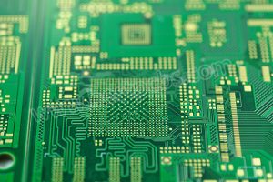
    You may also like