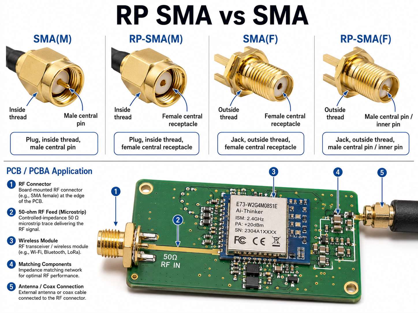
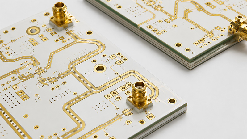
Searching for RP SMA vs SMA usually means one thing: you are trying to confirm whether an antenna, RF cable, module, or PCB connector will fit.
The difference looks small, but it can affect antenna matching, enclosure design, RF testing, and PCBA assembly. The key is simple: do not judge only by the outer thread. Check the center contact.
What Are SMA and RP-SMA Connectors?
SMA is a common RF coaxial connector used in GPS, cellular, RF test equipment, antennas, and many wireless products.
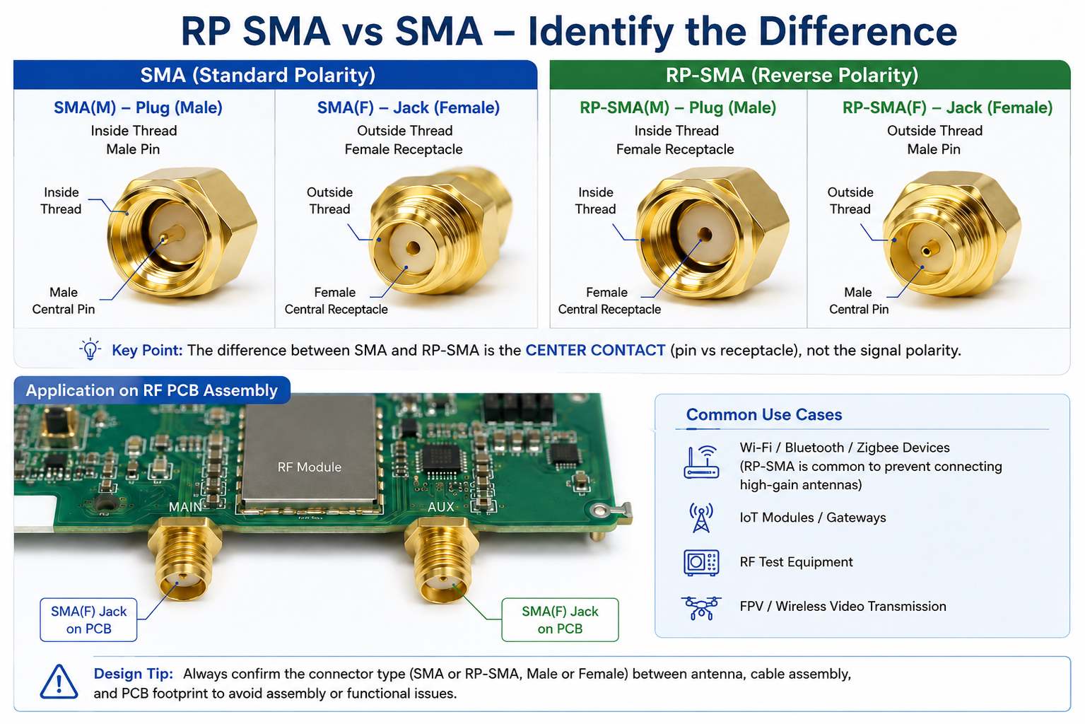
RP-SMA means Reverse Polarity SMA. It is a variation of SMA, but the center contact gender is reversed.
One important point: reverse polarity does not mean signal polarity is reversed. It only refers to the gender of the connector’s contact pin.
Why Was RP-SMA Created for Wireless Equipment?
RP-SMA was introduced to separate professional equipment from commercial wireless equipment.
The original purpose was to make it harder for users to connect high-gain professional antennas to consumer wireless devices and exceed regulatory limits.
That is why RP-SMA is widely seen in 2.4GHz wireless equipment, such as:
Wi-Fi
Bluetooth
Zigbee
IoT gateways
Some FPV devices
It is also linked with antenna compliance rules such as FCC Section 15.203 antenna requirements.
RP SMA vs SMA: What Is the Main Difference?
The main difference is the center contact.
Connector Type
Thread Type
Center Contact
SMA(M)
Plug, inside thread
Male central pin
SMA(F)
Jack, outside thread
Female central receptacle
RP-SMA(M)
Plug, inside thread
Female central receptacle
RP-SMA(F)
Jack, outside thread
Male central pin / inner pin
So the quick rule is:
SMA uses the standard center contact arrangement. RP-SMA reverses the center contact arrangement.
The outer housing can look similar. The center pin or center receptacle tells you the real connector type.
How to Tell SMA and RP-SMA Apart Quickly?
Use this 3-step check.
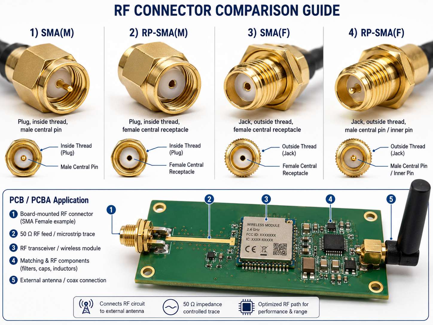
1. Check the thread
Plug = inside thread
Jack = outside thread
2. Check the center contact
A visible center pin = male central pin
A center hole = female central receptacle
3. Match the pattern
SMA(M): inside thread + male central pin
SMA(F): outside thread + female central receptacle
RP-SMA(M): inside thread + center receptacle
RP-SMA(F): outside thread + inner pin
This wording is important because many buyers only look at “male” or “female” in a product title. That is not enough for SMA and RP-SMA.
RP-SMA vs SMA Antenna: Which One Fits WiFi, Bluetooth, Zigbee, and FPV Devices?
RP-SMA is common in 2.4GHz wireless devices, especially Wi-Fi, Bluetooth, Zigbee, and consumer wireless equipment.
SMA is common in GPS, cellular, RF testing, industrial wireless, and many professional antenna systems.
For FPV systems, both SMA and RP-SMA may appear. Do not guess by frequency alone. Check the antenna connector and device connector.
Also, do not confuse connector type with antenna polarization.
SMA / RP-SMA = connector interface
RHCP / LHCP = antenna polarization
They are different specifications.
What Happens If You Choose the Wrong SMA or RP-SMA Connector?
A wrong connector choice can create several practical issues:
The antenna cannot be attached.
The RF cable does not mate with the board connector.
The test fixture needs an unexpected adapter.
The enclosure hole does not match the connector position.
The BOM causes purchasing confusion.
PCBA assembly may require rework.
Wireless testing gets delayed.
This is why connector details should be confirmed before PCB fabrication and PCBA assembly, not after samples arrive.
How Does SMA or RP-SMA Connector Choice Affect RF PCB and Wireless PCBA Design?
For an RF board project, SMA or RP-SMA is not just a purchasing item. It affects the board and assembly design.
Key design checks include:
50-ohm RF trace design
Connector footprint accuracy
Edge-launch or vertical mounting style
Ground pad and via placement
Antenna feed line length
Enclosure clearance
Connector solder joint strength
Cable and adapter compatibility
RF testing access
For wireless PCBA, the connector must match the antenna, cable, housing, and test plan. A small interface mistake can slow down the whole build.
This is where DFM review is useful. Before production, the PCB manufacturer should check the Gerber, BOM, connector datasheet, stackup, and RF layout together.
How to Choose the Right SMA or RP-SMA Connector for Your RF PCB Project?
Use this checklist before releasing files for production:
Confirm the wireless application: Wi-Fi, Bluetooth, Zigbee, GPS, cellular, FPV, or other RF use.
Check the antenna datasheet.
Confirm SMA or RP-SMA.
Confirm male central pin or female central receptacle.
Confirm plug inside thread or jack outside thread.
A clear BOM should not only say “SMA connector.” It should include the exact type, such as SMA(F), SMA(M), RP-SMA(F), or RP-SMA(M).
FAQs About RP SMA vs SMA
Q1. Is RP-SMA the same as SMA? No. RP-SMA is a variation of SMA, but the center contact gender is reversed.
Q2. What does reverse polarity SMA mean? It means the center contact gender is reversed. It does not mean the signal polarity is reversed.
Q3. How do I identify RP-SMA female? RP-SMA(F) is a Jack type with outside threads, but it has an inner pin.
Q4. How do I identify RP-SMA male? RP-SMA(M) has inside threads and a center receptacle.
Q5. Can SMA and RP-SMA connect directly? Usually not directly. If the center contacts do not match, you need the correct adapter.
Q6. Why is RP-SMA common on Wi-Fi equipment? It was widely used to support antenna compliance requirements and reduce casual connection of higher-gain antennas.
Q7. Is SMA common for GPS and cellular antennas? Yes. SMA connectors are generally used across GPS, cellular, RF testing, and industrial antenna systems.
Q8. Should I choose SMA or RP-SMA for my PCB? Choose based on the antenna, module, enclosure, regulatory needs, cable assembly, and test setup.
To sum up, the fastest way to understand RP SMA vs SMA is to check the center contact. SMA uses the standard center pin and receptacle arrangement. RP-SMA reverses that arrangement.
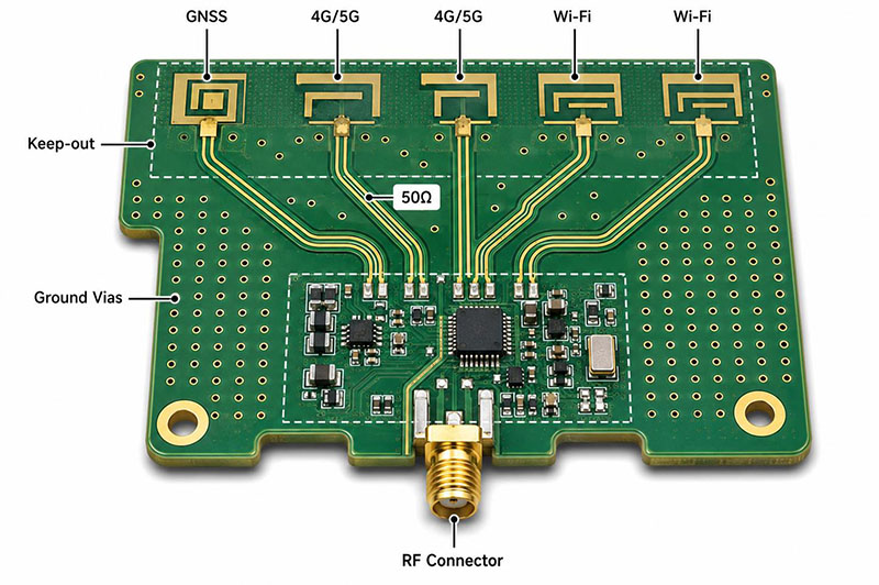
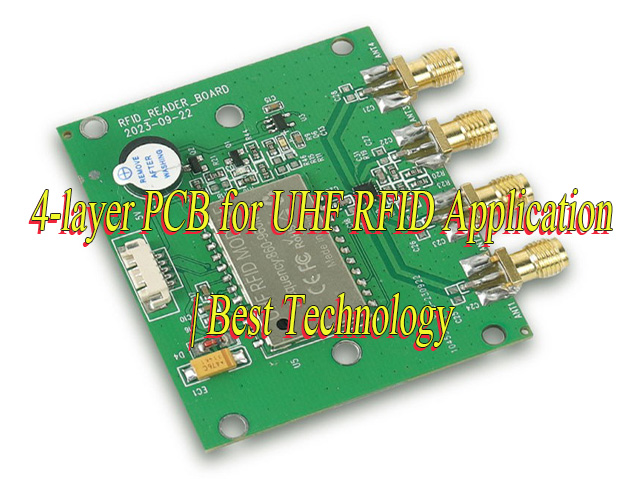
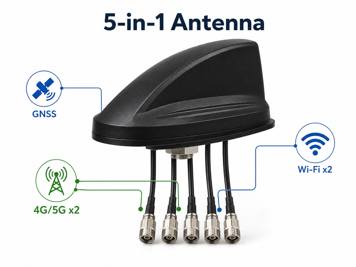
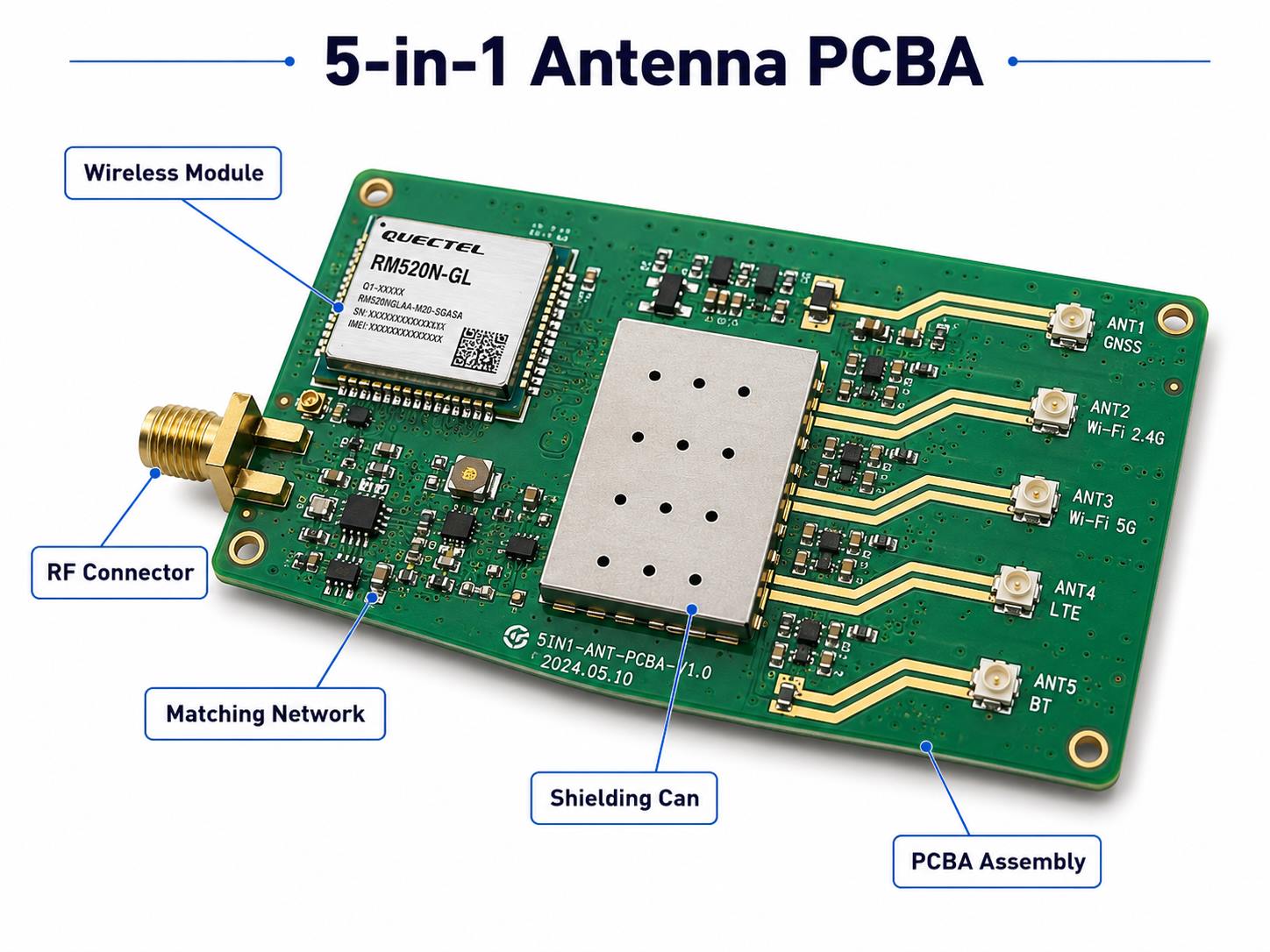
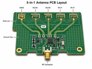
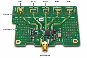
A 5-in-1 antenna usually combines GNSS, 4G/5G cellular, and Wi-Fi signal paths in one antenna unit. It is common in IoT gateways, vehicle trackers, industrial routers, smart transportation devices, and outdoor wireless terminals.
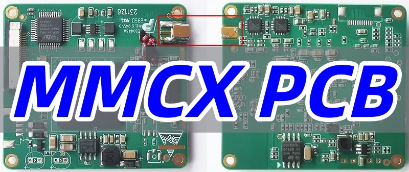
This guide focuses on the checks a PCB/PCBA manufacturer can realistically support before fabrication, assembly, and shipment. In many 5-in-1 antenna PCB and PCBA projects, the antenna is connected through RF interfaces such as SMA connector PCB, SMB PCB, UFL Connector PCB, BNC PCB, or MMCX PCB. If your wireless device requires RF connector assembly, controlled impedance PCB fabrication, or PCBA production review, you can send your Gerber files, BOM, and assembly requirements to sales@bestpcbs.com.
What Is a 5-in-1 Antenna?
A 5-in-1 antenna is an integrated antenna solution with five wireless signal paths. A common structure includes:
1x GNSS antenna
2x 4G/5G cellular MIMO antennas
2x Wi-Fi MIMO antennas
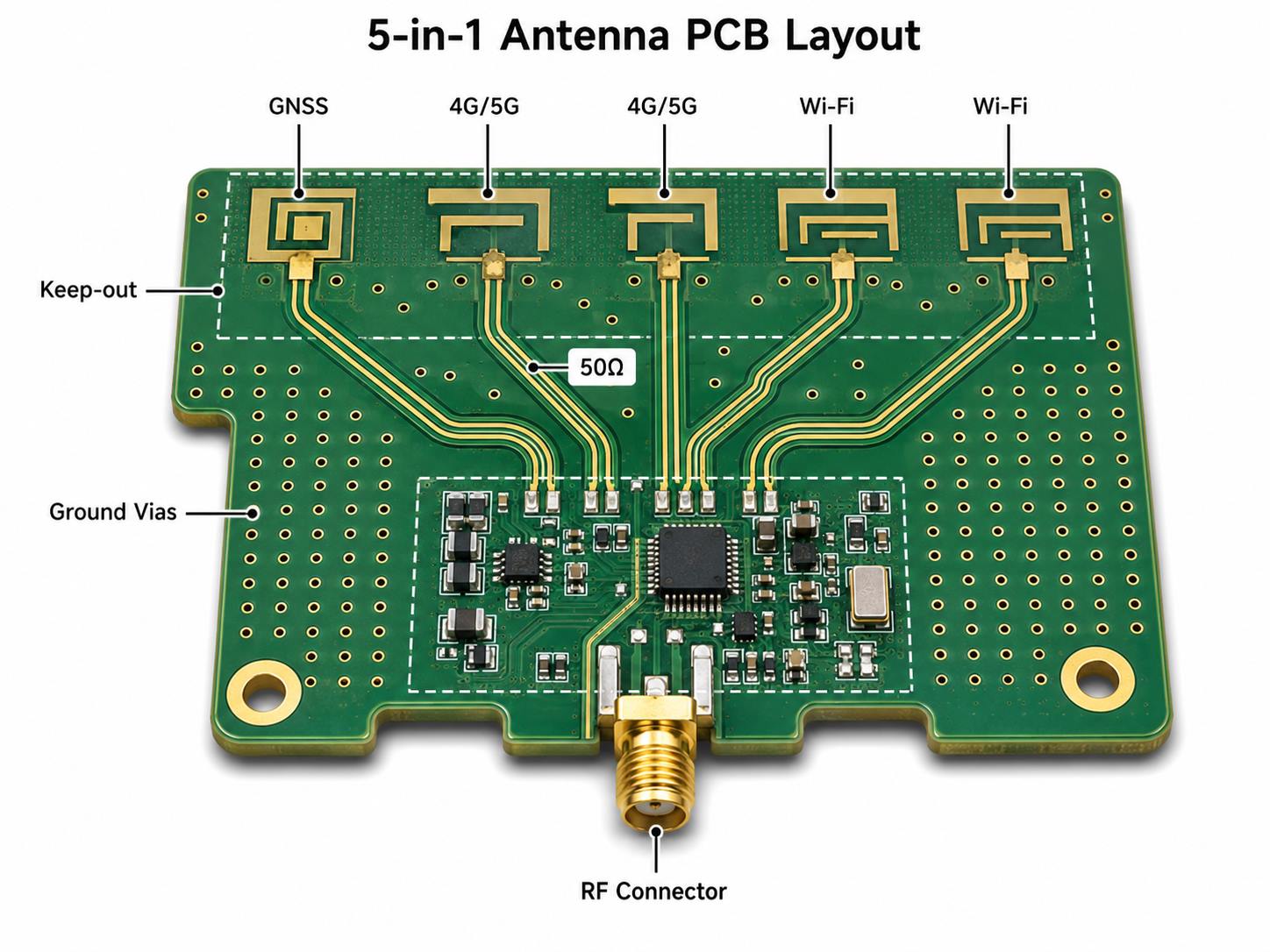
In a real device, the antenna connects to the PCB assembly through RF connectors, coaxial cables, wireless modules, matching circuits, ESD protection parts, and controlled impedance traces.
A PCB/PCBA manufacturer does not replace the antenna engineer. Its value is to check whether the PCB files, stackup, impedance notes, RF connector footprint, BOM, assembly drawing, and test requirements are ready for production.
Common PCB and PCBA Risks in 5-in-1 Antenna Projects
Connector datasheet, pad size, solder mask opening
RF matching issue
Wrong value or misplaced small components
BOM, placement file, first article inspection
Shielding issue
Poor soldering or incomplete grounding
Shielding can footprint, solderability, ground pads
These problems are expensive because they often appear after SMT assembly or final testing. Early manufacturing review is much cheaper than redesign, rework, or repeated debugging.
What Should Be Checked Before PCB Fabrication?
Before PCB fabrication, the main task is to confirm whether the board data can support stable RF-related production.
1. Stackup
Stackup affects impedance, trace width, return path, and signal loss. For antenna-related products, stackup should be confirmed before production.
Check:
Layer count
Dielectric thickness
Copper thickness
RF reference layer
Solder mask condition
Material availability
Impedance tolerance
2. 50Ω RF Trace Requirement
Most GNSS, cellular, and Wi-Fi feed lines use 50Ω controlled impedance. This requirement should be clearly marked in the fabrication notes.
Customers should provide:
Target impedance
Controlled impedance layer
Trace width and spacing
Stackup drawing
Impedance tolerance
Test coupon requirement
Without clear impedance notes, the board may be treated as a normal PCB instead of an RF-controlled board.
3. RF Connector Footprint
RF connector problems are common in antenna-related PCBA projects. SMA, U.FL, IPEX, MMCX, and board-to-board RF connectors all have specific footprint requirements.
Check:
Pad size
Ground pad connection
Solder mask opening
Connector orientation
Edge clearance
Cable direction
Rework space
A small footprint error can cause soldering defects, weak contact, or unstable field performance.
RF Connector Area and Assembly Clearance
The RF connector area should be reviewed before PCB fabrication and PCBA assembly. For a 5-in-1 antenna product, connector placement and nearby PCB details can affect soldering quality, cable installation, inspection, rework access, and production consistency.
A PCB/PCBA manufacturer can help check whether the connector footprint, solder mask opening, ground pads, board edge clearance, and cable direction match the assembly requirement. If the customer provides a wireless module layout guide or antenna reference design, the manufacturer can also review whether the board files follow the key manufacturing notes.
Check before production:
RF connector footprint against the datasheet
Pad size and solder mask opening
Ground pad connection around the connector
Board edge clearance
Cable plugging direction
Space for manual inspection and rework
Coaxial cable bend radius
Shielding can footprint and solderability, if used
Keep-out notes provided by the module or antenna supplier
This review does not replace antenna tuning, OTA testing, or RF chamber testing. Its purpose is to reduce assembly risk, connector failure, soldering defects, and avoidable layout-to-production problems.
What Types of PCBs Are Used in 5-in-1 Antenna Products?
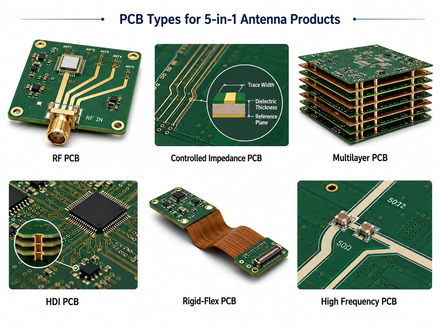
Different products need different PCB structures. The PCB type should match the RF requirement, space limit, assembly method, and working environment.
Smart LED or power products with wireless function
Helps thermal management
For many projects, the practical choice is a multilayer controlled impedance PCB. Compact products may use HDI PCB or rigid-flex PCB. Higher-frequency paths may require RF PCB or high frequency PCB.
What Should Be Checked During PCBA Assembly?
5-in-1 antenna PCBA assembly usually includes RF connectors, wireless modules, small matching components, shielding parts, and coaxial cables. These areas need tighter process control.
RF Connectors
Check connector position, solder quality, grounding, mechanical strength, and cable plugging direction. U.FL and IPEX connectors are small and can be damaged by poor soldering or repeated rework.
Wireless Modules
Check solder paste volume, stencil opening, reflow profile, placement accuracy, and inspection method. LGA, BGA, castellated, and fine-pitch wireless modules need stable SMT control.
Matching Network Components
Small capacitors and inductors near RF paths must match the BOM and placement file. Wrong values or wrong positions can change RF behavior.
Shielding Cans
Shielding only works well when grounding and soldering are reliable. Shielding can footprints, solder paste openings, and inspection standards should be confirmed before assembly.
Coaxial Cables and Wire Harnesses
Cable direction, bend radius, connector locking, strain relief, and final assembly sequence should be checked before batch production.
First Article Inspection
For the first build, inspect connector placement, module alignment, component value, polarity, solder joints, shielding position, and test results before moving to larger quantities.
What Testing Should Be Planned Before Shipment?
Testing should be defined before assembly, not after production is finished.
Test
Purpose
Bare PCB electrical test
Check opens and shorts
Impedance test
Confirm RF trace impedance on test coupon
AOI
Check solder joints, polarity, missing parts
X-ray
Inspect BGA/LGA or hidden solder joints
Functional test
Confirm power, module boot, interface communication
RF path continuity check
Find connector or soldering issues
GNSS/Wi-Fi/cellular function check
Verify product-level wireless function
Final assembly inspection
Check cable, connector, enclosure, label, and package
A PCB/PCBA factory can support production-level tests such as electrical test, impedance test, AOI, X-ray, visual inspection, and functional testing based on customer procedures.
Advanced antenna tests such as OTA, radiation pattern, antenna efficiency, and certification-level RF performance usually require customer fixtures, RF chambers, or third-party labs.
What Files Are Needed for a Faster Quote?
Complete files help the manufacturer review the project faster and quote more accurately.
Send:
Gerber or ODB++ files
Drill files
PCB stackup
Controlled impedance requirement
BOM with manufacturer part numbers
Pick-and-place file
Assembly drawing
RF connector datasheets
Wireless module datasheets
Antenna specification
Testing requirements
Cable or wire harness requirements
Order quantity
Target delivery schedule
For PCBA projects, BOM quality matters. RF connectors, wireless modules, EOL parts, and alternative components should be checked before batch production.
FAQs About 5-in-1 Antenna PCB and PCBA Manufacturing
Q1: Can a PCB/PCBA manufacturer design the 5-in-1 antenna? Usually no. A PCB/PCBA manufacturer supports layout review, DFM, impedance control, fabrication, assembly, and testing. Full antenna electromagnetic design should be handled by RF antenna specialists.
Q2: Does a 5-in-1 antenna PCB need controlled impedance? In most cases, yes. GNSS, cellular, and Wi-Fi RF feed lines commonly require 50Ω controlled impedance.
Q3: Can FR4 be used for 5-in-1 antenna products? Yes, FR4 can be used when the frequency, loss requirement, and layout structure are suitable. For higher-frequency or lower-loss paths, high frequency PCB materials may be needed.
Q4: What is the most common manufacturing issue? Common issues include unclear impedance notes, incorrect RF connector footprints, poor grounding, missing assembly clearance, wrong matching components, and poor cable routing.
Q5: What PCB type is commonly used? Many projects use multilayer controlled impedance PCB. Compact wireless products may use HDI PCB or rigid-flex PCB.
Q6: Can the factory test RF performance? The factory can support production-level tests. Advanced RF performance testing may require customer fixtures, RF chambers, or third-party RF labs.
In summary, a 5-in-1 antenna product is not difficult only because it uses several wireless functions. The real production challenge is making the PCB and PCBA stable, repeatable, and testable.
Before production, customers should confirm RF trace impedance, stackup, connector footprint, assembly clearance, shielding parts, cable routing, BOM accuracy, and test method. These checks help reduce rework, shorten debugging time, and improve batch consistency.
Best Technology supports RF PCB, high frequency PCB, controlled impedance PCB, multilayer PCB, HDI PCB, rigid-flex PCB, ceramic PCB, metal core PCB, PCB fabrication, PCBA assembly, SMT stencil, wire harness, component sourcing, DFM review, and production testing.
Send your Gerber files, BOM, antenna specification, and project requirements to sales@bestpcbs.com. Our engineering team can review your 5-in-1 antenna PCB and PCBA project before production and help you move from prototype to a more stable manufacturing build.
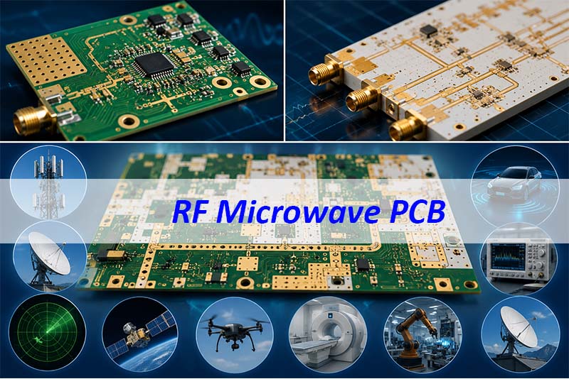
How can an RF microwave PCB keep high-frequency signals stable when small design and fabrication changes may affect the final result? This guide explains how RF microwave PCB boards work, how to choose suitable materials, how to control impedance and signal loss, and how to select the right manufacturer for prototype and production projects.
EBest Circuit (Best Technology) is an engineering-driven PCB and PCBA manufacturer with over 20 years of experience supporting high-frequency, RF, microwave, automotive, medical, industrial, communication, and aerospace/UAV projects. With self-owned PCB and PCBA factories, EBest provides DFM review, material selection support, controlled impedance PCB fabrication, component sourcing, assembly, testing, and production-quality support from prototype to mass production.
If you are evaluating an RF microwave PCB project and need practical manufacturing feedback, you can send your Gerber files, stackup, material requirements, and quantity to sales@bestpcbs.com for a technical review and quotation.
What Is an RF Microwave PCB Board?
An RF microwave PCB board is a printed circuit board made for radio frequency and microwave signals. It is a high-frequency circuit board designed for RF and microwave signal transmission, usually covering applications from MHz-level RF circuits to GHz and millimeter-wave systems.
In simple terms, RF board PCB is a broader category for radio-frequency circuits, microwave PCB usually refers to higher-frequency GHz-range circuits, and RF microwave PCB board is often used to describe a low-loss, impedance-controlled PCB built for both RF and microwave performance.
Unlike a standard FR4 PCB, an RF microwave PCB is part of the signal path. Therefore, the board does more than connect components. It also affects signal speed, loss, phase, reflection, and radiation.
In many low-speed PCB designs, small material changes may not create serious issues. However, RF and microwave circuits are more sensitive. A small shift in dielectric thickness, copper roughness, or trace width can change the final electrical behavior.
RF microwave PCB boards are commonly used in:
5G communication modules
RF antennas
Radar systems
Satellite communication equipment
Aerospace and UAV electronics
Industrial RF systems
Medical RF devices
Automotive radar and sensing modules
High-frequency test instruments
As a result, RF microwave PCB design must start with clear electrical goals. These goals may include low insertion loss, stable impedance, low return loss, strong grounding, and repeatable batch performance.
A well-built RF microwave PCB helps engineers reduce signal loss and improve circuit stability. It also makes the product easier to move from prototype to mass production.
How Does an RF Microwave High-Frequency PCB Work?
An RF microwave high-frequency PCB works by guiding electromagnetic energy through controlled signal paths. These paths may include microstrip lines, stripline traces, coplanar waveguides, grounded coplanar waveguides, and antenna feed lines.
At high frequencies, a copper trace is not just a simple wire. Instead, it works as a transmission line. The signal travels through both the copper and the surrounding dielectric field. Because of this, the material, trace width, spacing, ground plane, and via structure all affect performance.
Several factors matter most.
Impedance control is one of the first concerns. Many RF circuits use 50 ohm impedance, although some designs use other values. The final impedance depends on trace width, copper thickness, dielectric thickness, and dielectric constant.
Insertion loss is also important. It shows how much signal power is lost as the signal moves through the board. Loss can come from the dielectric material, copper surface, radiation, and poor transitions.
Return loss shows how much signal reflects back. Poor layout, sudden trace width changes, bad via design, or weak connector launch design may increase reflection.
Phase stability matters in radar, antenna, and communication systems. If the material or process changes too much, phase behavior may shift. This can affect signal timing and accuracy.
Ground return path is another key factor. RF current needs a clean return path. Therefore, a continuous ground plane and proper via stitching can help reduce noise, coupling, and radiation.
In short, an RF microwave PCB works well when the signal sees a stable path from the source to the load. Good design creates that path. Good fabrication keeps it consistent.
Where Are RF Microwave PCB Boards Used in 24GHz, 5G, and High-Power Applications?
RF microwave PCB boards are used in products where frequency, bandwidth, signal loss, and stability matter. Some boards are small antenna modules. Others are complex multilayer boards for communication systems.
Thermal control, material consistency, multilayer control
Aerospace and UAV
Lightweight and stable RF performance
Traceability, process control, vibration resistance
Industrial RF equipment
Reliable field operation
Strong structure, thermal reliability, test control
High-power RF modules
Heat control and signal stability
Metal-backed structure, thermal path, copper control
For a 24GHz RF microwave PCB, material choice and layout precision are already important. As the frequency rises, small geometry changes become more visible in actual RF performance.
For 5G-ready RF microwave high-frequency PCB fabrication, engineers often need low transmission loss, stable dielectric properties, and repeatable production. In many cases, they also need hybrid stackups. These stackups combine RF materials with FR4 or other support layers.
Meanwhile, high-power RF applications add another challenge: heat. These boards may need metal-backed structures, thermal vias, heavy copper areas, or a dedicated heat path.
Therefore, the best RF microwave PCB is not always the most complex board. It is the board that fits the signal, thermal, mechanical, and production needs of the product.
How to Do PCB Material Selection for RF Microwave Millimeter-Wave Design?
Material selection is one of the most important steps in RF microwave PCB design. The laminate affects signal loss, impedance, phase stability, heat control, and long-term reliability.
For PCB material selection for RF microwave millimeter-wave design, engineers usually check several material properties.
Material Factor
Why It Matters
Dielectric constant, Dk
Affects trace width, impedance, wavelength, and phase speed
Dissipation factor, Df
Affects dielectric loss, especially at high frequency
Copper roughness
Affects conductor loss and signal attenuation
Thermal conductivity
Helps move heat away from RF power areas
CTE
Affects dimensional stability and via reliability
Moisture absorption
Affects dielectric stability and long-term use
Process compatibility
Affects drilling, lamination, routing, and yield
Common RF microwave PCB materials include Rogers high-frequency laminates, PTFE-based laminates, ceramic-filled hydrocarbon materials, Taconic materials, and other low-loss substrates.
However, the lowest-loss material is not always the best choice. The project may also need cost control, easy sourcing, stable production, and strong mechanical performance. Therefore, engineers should choose the material based on frequency, loss target, thermal need, stackup, volume, and budget.
In some projects, a hybrid stackup is a practical choice. For example, the RF layer may use a low-loss material, while the support layers use FR4. This helps reduce cost while keeping the high-frequency path stable.
Before production, the material choice should be reviewed with the manufacturer. This can help avoid problems with drilling, lamination, copper control, and dimensional stability.
What Are the Main RF Microwave PCB Board Design and Layout Rules?
Good RF microwave PCB board design and layout starts with a clean signal path. The layout should reduce loss, avoid sudden impedance changes, and give RF signals a stable return path.
Here are the main design rules.
Keep RF traces short and direct.
Shorter traces reduce loss and lower the risk of unwanted coupling. Also, avoid unnecessary stubs, long detours, and sharp changes in direction.
Control impedance from the start.
The stackup, copper thickness, dielectric thickness, and trace width should be planned before layout. This helps avoid later redesign.
Use a continuous ground plane.
A broken ground plane can disturb the return path. As a result, it may increase radiation and impedance mismatch.
Add ground via stitching where needed.
Ground vias near RF traces can help control the electromagnetic field. They can also reduce coupling between nearby circuits.
Pay attention to via transitions.
At high frequency, a via can create unwanted inductance and capacitance. Therefore, via size, pad size, anti-pad size, and via depth should be reviewed.
Separate noisy circuits from RF areas.
Power converters, digital clocks, and fast switching signals should stay away from sensitive RF paths. In addition, proper shielding and layer planning can reduce noise.
Review solder mask over RF traces.
Solder mask can change impedance because it adds material above the copper. Some RF designs need solder mask clearance over controlled traces.
Design connector launches carefully.
A poor RF connector launch can create reflection and loss. Therefore, the launch area should match the connector type, stackup, and target impedance.
Overall, RF layout is not only about routing traces. It is about building a stable electrical environment around each signal path.
What Pain Points Come With RF Microwave PCB, and How Does EBest Solve Them?
RF microwave PCB projects often face issues that are not obvious at first. A board may look correct, but still fail RF testing. Therefore, early review and stable fabrication control are important.
Customer Challenge
What Usually Happens
How EBest Supports the Project
Material choice is unclear
The customer knows the frequency, but not the best laminate
EBest reviews frequency, Dk/Df, stackup, heat, cost, and production volume before giving material suggestions
Impedance is hard to control
Small trace or dielectric changes may cause reflection
EBest supports controlled impedance fabrication and checks stackup, trace width, copper thickness, and impedance targets before production
Prototype results are hard to repeat
The first sample may work, but later batches may shift
EBest helps control material batches, etching, lamination, inspection, and process records
Hybrid stackups create process risk
RF material and FR4 may behave differently during lamination
EBest reviews hybrid stackup feasibility and gives DFM suggestions before fabrication
RF designs need PCB and assembly support
Customers may need bare boards, components, assembly, and testing
EBest provides PCB fabrication, component sourcing, PCBA assembly, and testing support under one workflow
Design files are not production-ready
Small layout issues may lead to delay or rework
EBest provides DFM pre-review to help customers find risks before the board enters production
This structure keeps the problem and solution clear. It also helps buyers quickly see whether the manufacturer can support real project risks.
For RF microwave PCB projects, EBest does not only build boards from files. Instead, the engineering team can help review the practical manufacturing side of the design. This includes material selection, stackup, impedance control, trace tolerance, via design, and assembly needs.
As a result, customers can reduce trial-and-error during prototyping. They can also move more smoothly from sample builds to volume production.
How Does RF Microwave PCB Fabrication Control Impedance, Loss, and Tolerance?
RF microwave PCB fabrication requires stable process control. The goal is to keep the finished board close to the original electrical design.
Several fabrication steps affect RF performance.
Material handling
High-frequency materials may need special storage, drilling, lamination, and routing control. Good handling helps keep the material stable.
Stackup control
Dielectric thickness affects impedance. Therefore, prepreg flow, lamination pressure, and material selection must stay consistent.
Etching control
Trace width affects impedance and signal loss. The manufacturer must understand copper thickness and etching behavior. Then, it can apply proper compensation.
Copper thickness control
Uneven copper can change impedance. It can also affect conductor loss. Stable plating helps improve consistency.
Drilling and via quality
Vias affect RF transitions and board reliability. Clean drilling, proper desmear, and stable copper plating are important.
Surface finish selection
ENIG, immersion silver, OSP, and other finishes may affect solderability and surface behavior. The right finish depends on RF needs, assembly process, storage time, and customer standards.
Impedance testing
TDR testing and impedance coupons help confirm whether the board meets the target. This is especially important for controlled impedance RF circuits.
AOI and electrical testing
AOI checks trace quality and pattern accuracy. Electrical testing checks opens and shorts before shipment.
Because of these factors, a low-loss material alone cannot ensure good RF performance. The fabrication process must also be stable. In addition, the manufacturer must understand how each process step affects the final signal path.
How to Choose the Right RF Microwave PCB Manufacturer?
Choosing the right RF microwave PCB manufacturer is both a purchasing decision and an engineering decision. The supplier’s skill can affect signal performance, production yield, and delivery stability.
A reliable RF microwave PCB supplier should provide:
Experience with high-frequency materials
Controlled impedance fabrication
DFM review before production
Stackup and material support
Stable material sourcing
Prototype and small-batch support
Repeatable production control
AOI, electrical testing, and impedance testing
Clear communication about tolerance and process limits
Support for overseas customers
When requesting RF microwave PCB production quotes, customers should prepare clear data.
Required Information
Why It Matters
Gerber files
Allows the manufacturer to review the board accurately
Stackup
Helps confirm impedance and lamination structure
Material type
Affects cost, lead time, and RF performance
Copper thickness
Affects impedance and current capacity
Board thickness
Affects mechanics and signal structure
Surface finish
Affects assembly and solderability
Impedance target
Supports controlled impedance fabrication
Quantity
Affects pricing and delivery plan
Testing needs
Helps define inspection scope
Assembly needs
Helps plan PCB and PCBA together
A good manufacturer should not only quote the lowest price. It should also find material, design, process, or assembly risks before production. For RF microwave projects, this early review can save time and reduce avoidable cost.
Why EBest Is the Trusted RF Microwave PCB Partner for Global Brands?
EBest Circuit (Best Technology) supports customers that need reliable RF microwave PCB manufacturing from prototype to production. The company provides PCB fabrication, component sourcing, PCBA assembly, testing, and turnkey electronics manufacturing.
For RF microwave PCB projects, EBest’s value is not only in board production. It also comes from engineering support before production starts.
Engineering-driven review
EBest provides DFM pre-review for material choice, stackup, impedance, copper thickness, trace width, via structure, and manufacturability.
High-frequency material experience
The team supports Rogers and other low-loss laminates. It can also support hybrid stackups when customers need a balance of RF performance and cost.
PCB and PCBA support
Many RF products need more than bare PCB fabrication. Therefore, EBest can support component sourcing, SMT assembly, testing, and final production coordination.
Quality system support
EBest works with quality systems suitable for demanding industries, including ISO9001, ISO13485, IATF16949, AS9100D, and UL-related PCB manufacturing support depending on project needs.
Prototype to mass production
RF products often move through several validation stages. EBest supports quick prototyping, small-batch builds, and production orders. This helps customers keep the same manufacturing logic across the project.
Industry experience
EBest serves communication, medical device, industrial control, automotive electronics, aerospace/UAV, lighting, robotics, new energy, and instrument applications.
For customers looking for a reliable RF microwave PCB manufacturer, EBest can review design files, support material selection, provide fabrication suggestions, and offer production quotes based on real project needs.
To discuss an RF microwave PCB project, customers can contact sales@bestpcbs.com with Gerber files, stackup, material requirements, quantity, and assembly needs.
FAQs About RF Microwave PCB
What is the difference between RF PCB and microwave PCB? RF PCB is a broad term for boards that carry radio frequency signals. Microwave PCB usually refers to boards that work at higher frequencies. In many searches, the term RF microwave PCB covers both types.
What materials are commonly used for RF microwave PCB fabrication? Common materials include Rogers laminates, PTFE-based laminates, ceramic-filled hydrocarbon materials, low-loss RF substrates, and hybrid RF plus FR4 stackups.
Can RF microwave PCB be used for 24GHz and 5G applications? Yes. RF microwave PCB boards can be used in 24GHz radar, 5G RF modules, antennas, communication systems, and high-frequency sensing products. Here, 24GHz usually refers to radar applications, while 2.4GHz is more commonly used for WiFi, Bluetooth, Zigbee, and other ISM-band wireless devices.
Where can I get metal-backed RF microwave PCB boards? You can get metal-backed RF microwave PCB boards from manufacturers with both RF material experience and thermal management capability.
EBest Circuit (Best Technology) can provide metal-backed RF microwave PCB boards using aluminum or copper base structures to support heat dissipation in high-power RF and microwave applications. For projects that need low-loss materials, controlled impedance, and stable thermal performance, EBest can also support DFM review, material selection, PCB fabrication, assembly, and testing.
Does RF microwave PCB require controlled impedance? In most cases, yes. Controlled impedance helps reduce reflection and signal loss. Many RF traces use 50 ohm impedance, but the final value depends on the circuit design.
Can EBest support RF microwave PCB assembly? Yes. EBest supports RF microwave PCB fabrication, component sourcing, SMT assembly, testing, and turnkey electronics manufacturing.
How do I request RF microwave PCB production quotes? Prepare Gerber files, stackup, material type, copper thickness, board thickness, surface finish, impedance target, quantity, and assembly needs. Clear data helps the manufacturer quote faster and more accurately.
If you are not sure whether your RF microwave PCB design is ready for production, EBest Circuit (Best Technology) can review your files and provide practical manufacturing feedback. You can send your Gerber files and project requirements to sales@bestpcbs.com for a technical review and quotation.
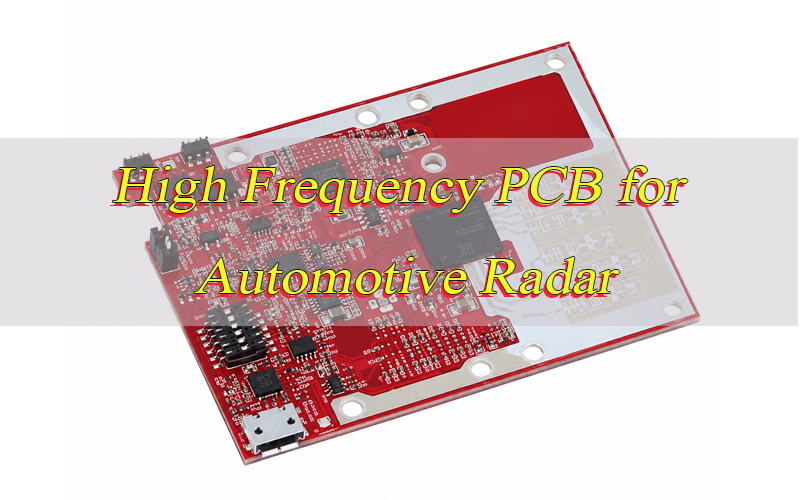
How can high frequency PCB for automotive radar help reduce signal loss and improve 77GHz ADAS module stability? In automotive radar design, small changes in material, stackup, antenna geometry, or impedance can affect detection range and signal consistency. This guide explains the practical PCB factors that influence radar performance, from material selection and DFM review to surface finish, reliability control, and mass production support.
How Does a High Frequency PCB for Automotive Radar Work in a 77GHz Radar Module?
A high frequency PCB inside a 77GHz radar module is not only used to connect components. It also supports RF signal transmission, antenna behavior, grounding, power distribution, and mechanical integration inside the radar housing. Because the radar signal works at millimeter-wave frequency, the PCB structure becomes part of the signal path.
It transfers RF signals from the radar IC to the antenna area The radar transceiver generates high-frequency signals. These signals move through microstrip lines, stripline structures, feedlines, vias, and antenna networks on the PCB. At 77GHz, even a small change in line width, dielectric thickness, or copper surface condition may affect insertion loss and impedance.
It may form the antenna directly on the board Many automotive radar modules use PCB antenna arrays. In this design, antenna patches or antenna feed networks are created by copper patterns. The PCB manufacturer is not just fabricating copper traces. It is producing a functional RF structure.
It helps receive reflected signals Radar signals are transmitted outward and reflected by vehicles, pedestrians, road barriers, or nearby objects. The receiving antenna collects the reflected signal and routes it back to the radar IC. The radar system then calculates distance, speed, angle, and movement.
It provides a stable ground reference Ground layers are critical in radar PCB design. A continuous ground plane helps reduce unwanted radiation, signal reflection, and noise coupling. If the ground path is broken or poorly connected, the RF path may become unstable.
It supports power, digital, and interface circuits A radar PCB may also include power management circuits, MCU or DSP control sections, CAN interface, Ethernet interface, shielding contacts, and connectors. These areas should be arranged carefully to avoid interference with sensitive RF sections.
It must fit the radar enclosure The PCB must match the radar housing, radome, connector position, screw holes, thermal path, and shielding cover. Poor mechanical matching may create stress, warpage, or assembly difficulty.
In short, the board is part of the radar system. Good PCB design helps the radar module perform more consistently during testing, assembly, and long-term vehicle operation.
Where Is High Frequency PCB Used in Automotive Radar Applications?
High frequency PCB is used in different radar positions around the vehicle. Each position has different requirements for detection range, field of view, module size, antenna arrangement, and environmental reliability. That is why one radar PCB design may not be suitable for all automotive radar applications.
Front long-range radar Front radar is commonly used for adaptive cruise control, forward collision warning, and automatic emergency braking. These modules need stable long-distance signal transmission. The PCB should offer low RF loss, accurate antenna geometry, and good phase consistency.
Corner radar Corner radar is used for blind spot detection, lane change assistance, and cross-traffic alert. These modules are usually compact, so the PCB needs efficient antenna layout and controlled RF routing in a limited space.
Rear radar Rear radar supports reverse warning, rear collision detection, and parking assistance. The PCB must maintain stable performance in environments where moisture, vibration, dust, and temperature changes may occur.
Short-range radar Short-range radar is often used for parking systems and nearby object detection. The PCB may require dense antenna structures and precise copper pattern control because the module needs accurate short-distance sensing.
In-cabin radar In-cabin radar can be used for occupant sensing, child presence detection, and gesture recognition. These boards often need compact layout, controlled radiation behavior, and good compatibility with plastic housings.
Advanced imaging radar Imaging radar requires more channels and higher signal processing capability. The PCB may need tighter phase control, more complex routing, and better production repeatability.
For all these applications, the PCB must do more than meet basic electrical continuity. It must support stable radar sensing under real vehicle conditions.
What PCB Material Should Be Used for 77GHz Automotive Radar?
Material selection is one of the most important decisions in a high frequency PCB for automotive radar. The substrate controls dielectric loss, signal speed, antenna resonance, impedance behavior, and long-term stability. A material that works well for ordinary control circuits may not be suitable for 77GHz RF transmission.
Low-loss high-frequency laminate is usually required for the RF area At 77GHz, dielectric loss becomes a major concern. A low-loss material helps reduce signal attenuation from the radar IC to the antenna. This is especially important for front radar and long-range sensing.
Stable Dk helps maintain predictable antenna behavior Dk means dielectric constant. If Dk changes too much with frequency, temperature, or production batch, the antenna and RF traces may behave differently from the design model. Stable Dk helps keep the radar frequency response more predictable.
Low Df helps reduce energy loss Df means dissipation factor. Lower Df usually means lower dielectric loss. For millimeter-wave radar, this helps preserve signal strength and improve RF efficiency.
Copper foil type should be reviewed Copper roughness matters at high frequency. Rougher copper may increase conductor loss. For sensitive RF feedlines and antenna areas, smoother copper can support more consistent signal transmission.
FR4 can be used only in non-critical areas FR4 may be suitable for digital control, power circuits, or mechanical support layers. However, it is usually not a good choice for 77GHz antenna and RF feedline areas because its dielectric properties are not stable enough for high-performance millimeter-wave transmission.
Hybrid stackup is common in radar modules Many radar boards combine high-frequency laminate for the RF layer with FR4 for digital or power layers. This can reduce total cost while keeping the RF area stable.
Material availability matters for mass production A material may perform well in prototype, but if it is difficult to source consistently, it may create problems later. Engineers should confirm material availability before approving the design for production.
A practical material choice should balance RF performance, cost, manufacturability, reliability, and supply stability.
How Should the PCB Stackup Be Designed for Automotive Radar?
Stackup design controls how copper layers, dielectric materials, ground planes, and signal paths work together. For automotive radar, stackup is not just a mechanical layer arrangement. It directly affects RF performance, antenna behavior, impedance control, warpage, and assembly quality.
Place the RF antenna layer carefully Many radar modules place the antenna on the top layer. This makes copper geometry, surface finish, and solder mask control very important. If the antenna layer is changed later, the radar performance may need to be revalidated.
Control dielectric thickness tightly The distance between the antenna copper and ground plane affects antenna resonance and impedance. Loose dielectric thickness tolerance may cause frequency shift or inconsistent signal behavior.
Use a continuous ground reference layer A stable ground plane helps control RF return current and reduce unwanted coupling. Ground voids, splits, or poorly connected areas may create unpredictable RF results.
Review hybrid lamination carefully If the board combines high-frequency laminate and FR4, the manufacturer must check bonding strength, thermal expansion difference, lamination pressure, and warpage risk.
Keep the structure balanced A symmetrical or well-balanced stackup helps reduce board bending. This is important for SMT assembly, radar IC mounting, shielding installation, and final module assembly.
Manage RF vias and transitions Poor via transitions can create impedance discontinuity. Long via stubs, weak grounding, or uncontrolled launch structures may reduce signal quality.
Separate RF, digital, and power areas Switching power circuits and digital signals should be kept away from sensitive RF paths. Proper layer planning helps reduce coupling and noise.
Keep the approved stackup unchanged after validation Once a radar board passes RF validation, changes to material, dielectric thickness, copper type, or layer sequence should be controlled carefully.
A good stackup design reduces the gap between simulation, prototype testing, and real production results.
Why Is Antenna Area Control Critical in Automotive Radar PCB Manufacturing?
The antenna area is one of the most sensitive regions on a high frequency PCB for automotive radar. When the antenna is formed directly by copper patterns, the PCB manufacturer is effectively producing the radar’s transmitting and receiving structure. This area needs much tighter control than ordinary signal routing.
Antenna dimensions affect frequency response If the antenna patch is slightly larger or smaller than designed, the antenna response may shift. Over-etching or under-etching can change the effective antenna size.
Feedline accuracy affects matching The feedline connects the radar IC to the antenna. If the line width or spacing changes, impedance may shift and signal reflection may increase.
Element spacing affects phase consistency Radar antenna arrays depend on consistent spacing between antenna elements. Uneven spacing may affect angle detection and beam behavior.
Solder mask can change the dielectric environment If solder mask covers an area that should remain open, it may change local capacitance and dielectric loading. This can affect antenna performance.
Surface finish may influence RF behavior Different finishes have different metal layers and thicknesses. In sensitive antenna regions, the finish should be selected and controlled carefully.
Layer alignment must be controlled The antenna layer and reference ground layer need proper alignment. Misregistration may affect the RF field and antenna behavior.
Panelization can influence consistency The position of the board inside the production panel may affect etching uniformity. For radar antenna arrays, the manufacturer should consider whether the panel layout creates dimensional variation.
Before production, the drawing should clearly define antenna tolerance, solder mask opening, copper thickness, surface finish, inspection points, and RF keep-out areas.
How Does Controlled Impedance Affect Radar Signal Transmission?
Controlled impedance helps RF signals travel through the PCB with predictable behavior. If impedance changes along the signal path, part of the signal may reflect back. In radar modules, this can increase loss, reduce signal quality, and make calibration more difficult.
Trace width must match the stackup A 50-ohm RF line depends on trace width, dielectric thickness, copper thickness, and material Dk. The manufacturer should calculate the line width based on real material data.
Etching tolerance affects impedance If the finished trace is narrower or wider than expected, impedance changes. For 77GHz designs, this variation can be significant.
Reference plane distance must be stable The distance between RF trace and ground layer controls impedance. If dielectric thickness varies, impedance may drift.
Solder mask condition should be confirmed Whether the RF trace is covered by solder mask or exposed can affect impedance. This should be defined before production.
Vias and bends need special attention RF vias, bends, launch structures, and transitions may create discontinuity. Smooth transitions help reduce reflection.
Impedance coupons may be required Test coupons help verify whether the fabricated board meets impedance requirements. They are useful for production control.
Repeat orders must follow the approved process Material substitution, copper thickness change, or stackup change may alter impedance. Such changes should not be made without engineering review.
Controlled impedance is not a decoration on the drawing. It is a manufacturing requirement that directly affects radar signal stability.
What Are the Main Manufacturing Challenges of Automotive Radar PCB?
Automotive radar PCB manufacturing is difficult because it combines millimeter-wave RF requirements with automotive-level consistency. The manufacturer must control fine copper features, hybrid materials, surface finish, flatness, and inspection records at the same time.
Fine RF trace etching Small RF lines and gaps need precise etching compensation. If the etching process is unstable, impedance and antenna geometry may shift.
Antenna copper accuracy Antenna patterns must match the design closely. Small copper deviations can affect resonance, gain, and phase response.
Hybrid material lamination High-frequency materials and FR4 may expand differently during lamination. This can create warpage, bonding stress, or registration issues.
Copper roughness control At 77GHz, the copper surface becomes important. The manufacturer should understand how copper foil type affects conductor loss.
Via plating quality Radar boards may include dense grounding vias and signal transitions. Poor via plating can reduce reliability and affect electrical performance.
Solder mask registration Mask shift near antenna or RF traces may change the local RF environment. Mask opening requirements must be followed accurately.
Board flatness Warpage can affect SMT assembly and module housing installation. A warped PCB may also create stress on radar ICs or connectors.
Surface finish consistency The finish must support both soldering and RF requirements. Inconsistent finish thickness may create assembly or performance concerns.
Batch repeatability Automotive customers need stable quality over time. The same material, process, and inspection method should be used from prototype to mass production.
The real challenge is not producing one good sample. It is producing stable boards again and again.
How Should DFM Review Be Done Before Automotive Radar PCB Production?
DFM review is a key step before producing a high frequency PCB for automotive radar. Many RF problems are hard to fix after the board has been fabricated. A good DFM review can identify risks before they become expensive prototype failures.
Check the material specification The manufacturer should confirm laminate brand, grade, thickness, copper type, and material availability. Any unclear material description should be clarified before quotation or production.
Review the stackup carefully Stackup review should include dielectric thickness, copper thickness, layer sequence, ground reference, and hybrid lamination feasibility.
Confirm impedance requirements The target impedance, tolerance, trace width, and test method should be confirmed. If the drawing only says “controlled impedance” without details, the manufacturer should ask for clarification.
Inspect the antenna area The antenna pattern should be reviewed for copper tolerance, solder mask opening, surface finish, and dimensional inspection needs.
Check solder mask rules RF traces and antenna patches may need larger solder mask clearance or complete mask opening. This should not be left to default factory rules.
Review via structures The manufacturer should check via placement, grounding vias, via stubs, via-in-pad risk, and plating requirements.
Confirm surface finish The finish should support both SMT assembly and RF performance. For sensitive RF areas, the finish selection may need extra review.
Evaluate copper balance and warpage risk Uneven copper distribution may cause board bending. Copper balancing should be reviewed without disturbing RF areas.
Review panelization Panel design should support stable etching, assembly handling, and antenna consistency.
Define inspection requirements AOI, impedance testing, electrical testing, microsection, dimensional inspection, and final inspection should be specified clearly.
A strong DFM review helps customers reduce avoidable errors and prepare the design for repeatable production.
What Surface Finish Is Suitable for Automotive Radar PCB?
Surface finish protects exposed copper and supports soldering. In automotive radar PCB, it may also affect RF performance, especially when antenna patterns or RF feedlines are exposed. The best finish depends on the antenna design, assembly process, storage time, and reliability requirements.
ENIG ENIG offers good solderability, flatness, and storage stability. It is commonly used in many PCB applications. However, the nickel layer should be reviewed when it appears in RF-sensitive areas.
Immersion silver Immersion silver provides a flat and conductive surface. It can be suitable for RF applications, but storage and handling conditions should be controlled to avoid tarnish or contamination.
OSP OSP is flat and simple. It avoids extra metal layers, which may be useful in some RF designs. However, it has shorter shelf life and requires careful assembly planning.
Immersion tin Immersion tin provides a flat solderable surface. It may be used in some designs, but process control and whisker risk should be considered.
Selective finish Some radar boards may need different treatment for antenna areas and component soldering pads. This should be clearly marked in the fabrication notes.
When selecting surface finish, we should consider:
Whether the antenna area needs exposed copper
Whether nickel is acceptable in RF areas
Whether the radar IC requires fine-pitch assembly
How long the boards will be stored before SMT
Whether the finish meets automotive reliability requirements
Whether drawing notes clearly separate RF and soldering areas
Surface finish should not be selected only for solderability. For radar boards, RF behavior and assembly reliability must be reviewed together.
How to Ensure Reliability for High Frequency PCB for Automotive Radar in Harsh Environments?
Automotive radar modules work in demanding environments. They may face high temperature, low temperature, vibration, humidity, dust, road salt, and long service life. The PCB must remain stable both electrically and mechanically.
Material traceability Material batch records should be kept for laminate, prepreg, copper foil, surface finish chemistry, and other key production materials.
Lamination process control Temperature, pressure, time, and bonding quality should be controlled during lamination. This is especially important for hybrid stackups.
Copper plating inspection Hole wall copper thickness and plating quality affect long-term reliability. Poor plating can create failures under thermal cycling or vibration.
AOI inspection AOI helps detect open circuits, shorts, under-etching, over-etching, and copper pattern issues in RF and antenna areas.
Electrical testing Electrical testing confirms continuity and isolation. It is a basic but important step before shipment.
Impedance verification Impedance testing helps confirm that the RF transmission path matches design requirements.
Dimensional inspection Critical antenna dimensions should be inspected when required. This helps control RF consistency.
Solderability testing Surface finish quality should support reliable SMT assembly.
Ionic contamination control Cleanliness matters for long-term reliability. Residue on the board may create leakage or corrosion risk.
Warpage inspection Board flatness should be checked, especially when radar ICs, shields, or connectors require precise assembly.
Documentation control Inspection reports, material records, and shipment traceability should be available for customer review.
Reliability is not created by one final test. It comes from stable material, controlled process, careful inspection, and complete documentation.
How Can a Manufacturer Support High Frequency PCB for Automotive Radar Projects?
A qualified PCB manufacturer should support the project before production begins. For 77GHz radar PCB, early communication can help customers reduce design risk, control cost, and improve the chance of successful validation.
Material selection support The manufacturer can help compare high-frequency laminates based on Dk, Df, copper type, thickness, availability, and cost.
Stackup review The manufacturer can check whether the stackup supports impedance, antenna behavior, lamination, and board flatness.
Controlled impedance calculation Trace width should be calculated using real laminate data and finished copper thickness. This helps reduce mismatch between design and production.
DFM pre-check The manufacturer can review antenna areas, RF traces, solder mask openings, vias, surface finish, panelization, and assembly risks.
Prototype fabrication Prototype boards should be made with production-aware methods. This helps make later small-batch production smoother.
Small-batch production support After prototype validation, the manufacturer should keep the approved material, stackup, and process conditions stable.
Mass production consistency For automotive projects, consistency matters as much as capability. The manufacturer should maintain clear process records and inspection standards.
Inspection and testing support AOI, electrical testing, impedance testing, microsection, X-ray when required, and dimensional inspection help improve quality confidence.
Traceability support Material and production records help customers manage automotive quality requirements and future audits.
Assembly coordination Radar modules often require fine-pitch components, shields, connectors, and thermal structures. PCB fabrication should be reviewed together with SMT assembly needs.
EBest Circuit supports high-frequency PCB fabrication, controlled impedance production, hybrid stackup review, DFM pre-check, prototype manufacturing, and batch production for automotive electronics, RF modules, radar boards, communication equipment, and advanced sensing applications.
Application Case: Solving a 77GHz Radar PCB Prototype Issue
Customer Background
A customer was developing a compact 77GHz automotive radar module for ADAS testing. The PCB included radar IC pads, RF feedlines, PCB antenna patterns, digital control circuits, and power management sections. The customer needed prototype boards for functional testing before moving to a pilot run.
Project Challenge
During the initial engineering review, several risks were found:
The RF layer material was not clearly specified.
Dielectric thickness tolerance was missing.
Antenna solder mask opening was not defined.
Some RF feedlines required impedance confirmation.
Hybrid stackup created possible warpage risk.
Critical antenna dimensions were not marked for inspection.
Surface finish notes did not separate RF and soldering requirements.
Panelization had not been reviewed for antenna consistency.
These issues could affect both prototype testing and future repeat production. Even if the board passed basic electrical testing, the radar module might still show unstable RF performance.
Our Solution
The engineering team reviewed the Gerber files, stackup, material options, antenna layout, RF traces, and fabrication notes. Then several practical improvements were suggested:
Confirmed a suitable high-frequency laminate for the RF antenna layer.
Clarified dielectric thickness and finished copper requirements.
Defined solder mask opening for antenna and RF-sensitive areas.
Reviewed controlled impedance traces before production.
Checked copper balance to reduce warpage risk.
Added inspection points for antenna dimensions.
Confirmed surface finish requirements for assembly and RF areas.
Reviewed panelization to improve production consistency.
Prepared clearer production notes for repeat orders.
Result
The revised prototype was easier to fabricate and more suitable for radar module validation. The customer completed SMT assembly and used the boards for functional testing. After design confirmation, the project moved toward small-batch production with clearer manufacturing requirements.
This case shows a practical point: in 77GHz radar PCB projects, small details can affect both RF performance and production repeatability. Early DFM review helps reduce avoidable delays and supports smoother project transfer.
FAQs About High Frequency PCB for Automotive Radar
Q1: What frequency range is commonly used in modern automotive radar? A1:Many modern automotive radar modules operate around 77GHz, often within the 76GHz to 81GHz range. This range supports distance detection, speed measurement, and object tracking for ADAS functions.
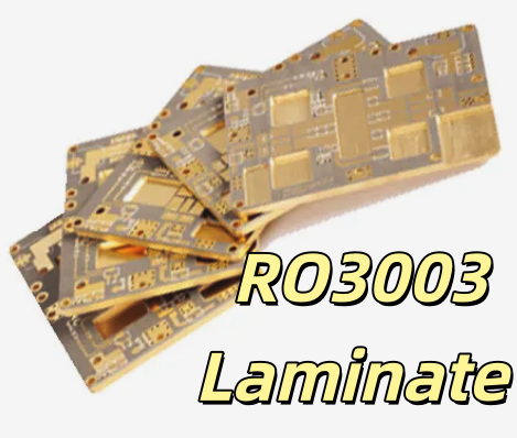
Q2: Is RO3003 the only material choice for 77GHz radar PCB? A2:No. RO3003 is a common option, but other low-loss high-frequency laminates may also be suitable. The final choice depends on antenna design, loss target, stackup, cost, and production stability.
Q3: Can FR4 be used anywhere in a radar PCB? A3:Yes. FR4 can be used in digital, power, or mechanical support areas. However, the 77GHz RF feedline and antenna areas usually need low-loss high-frequency material.
Q4: Why is copper roughness important in millimeter-wave PCB design? A4:At high frequency, current flows close to the copper surface. Rough copper can increase conductor loss. Smoother copper helps improve RF consistency.
Q5: Should solder mask be removed from radar antenna areas? A5:It depends on the antenna design. Some antenna areas require solder mask opening to avoid changing the local dielectric environment. This should be clearly defined in the fabrication drawing.
Q6: Why can a radar PCB prototype pass once but fail in later production? A6:Possible reasons include material substitution, dielectric thickness drift, copper tolerance variation, surface finish change, panelization difference, or unclear production notes.
Q7: What files should customers provide for radar PCB quotation? A7:Customers should provide Gerber files, stackup, material requirement, copper thickness, impedance data, surface finish, solder mask notes, antenna tolerance, inspection requirements, and expected quantity.
Q8: What is the biggest mistake in 77GHz radar PCB preparation? A8:A common mistake is treating the antenna area like normal copper artwork. In reality, antenna geometry, solder mask, surface finish, and dielectric thickness all affect radar performance.
Q9: Does surface finish affect automotive radar PCB performance? A9:It may affect sensitive RF areas, especially when antenna patterns or feedlines are exposed. The finish should be selected based on both soldering needs and RF behavior.
Q10: Why is DFM review important before radar PCB production? A10:DFM review helps identify risks before fabrication. It can prevent issues related to material choice, stackup, impedance, antenna copper, solder mask, via design, warpage, and surface finish.
Conclusion
A high frequency PCB for automotive radar must support stable 77GHz signal transmission, accurate antenna behavior, controlled impedance, and reliable operation in harsh vehicle environments. It is part of the radar module’s RF performance, not only a carrier for electronic components.
For successful development, customers should review material selection, stackup design, antenna area control, impedance management, solder mask strategy, surface finish, DFM feedback, inspection plan, and traceability records before production starts.
A professional high-frequency PCB manufacturer can help reduce prototype risk and improve production consistency. With early engineering review and controlled manufacturing, automotive radar PCB projects can move more smoothly from design validation to mass production.
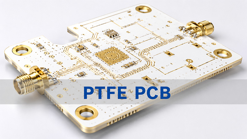
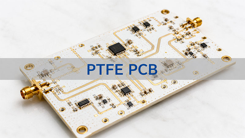
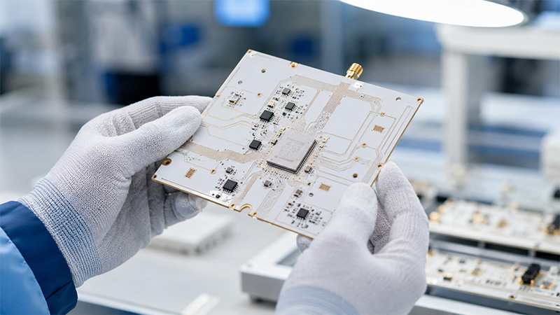
PTFE PCB projects usually come with clear business goals: stable RF performance, reliable fabrication, smooth assembly, and fewer delays before production. For buyers, the key question is not only “What is PTFE?” It is also “Can this manufacturer support my material, stack-up, impedance, RF connector assembly, and delivery needs?”
This guide helps you compare PTFE PCB materials, manufacturing capabilities, application fit, DFM support, and supplier selection factors.
What Is a PTFE PCB and Is It Right for Your Project?
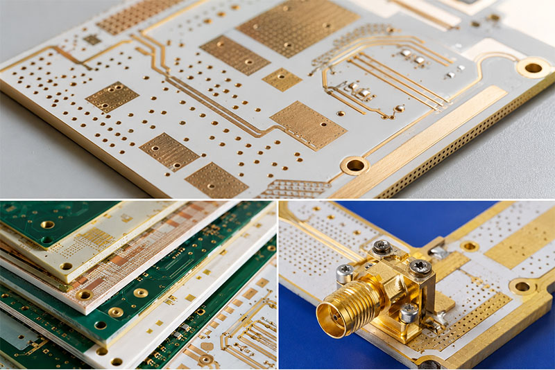
A PTFE PCB is a printed circuit board made with PTFE-based dielectric material. Engineers often choose it for RF, microwave, antenna, radar, and high-frequency communication products.
Can the supplier control material, impedance, drilling, and assembly?
When PTFE PCB Is a Good Fit
Your Project Need
Why PTFE Helps
RF signal transmission
Supports lower dielectric loss
Microwave circuit design
Helps keep signal behavior stable
Antenna board development
Supports controlled impedance and phase stability
Radar or communication module
Works well in high-frequency environments
Low-loss signal path
Reduces signal attenuation compared with standard FR4
When FR4 May Still Be Enough
Project Condition
Better Choice
Low-frequency control board
FR4
Cost-sensitive general electronics
FR4
Simple power or LED board
FR4 or MCPCB
RF, microwave, radar, or antenna product
PTFE or other high-frequency laminate
Quick takeaway: Choose PTFE when signal quality matters more than material cost.
What PTFE PCB Materials and Laminates Can You Choose?
Material choice affects loss, impedance, lead time, cost, and long-term reliability. Buyers should not choose a laminate only by brand name. The material should match the frequency, stack-up, copper weight, and production plan.
Material / Laminate Type
Common Use
Buyer Benefit
PTFE Laminate
RF and microwave boards
Low loss and stable electrical behavior
Rogers PTFE-Based Materials
Antenna, radar, telecom, aerospace electronics
Strong RF performance and trusted material data
Taconic Materials
RF modules, microwave circuits, antennas
Good high-frequency options for different budgets
Arlon Materials
RF, military, aerospace, and communication boards
Good fit for demanding high-frequency circuits
Nelco Materials
High-speed and RF-related boards
Useful for signal integrity and stable fabrication
Hybrid PTFE + FR4 Stack-Up
Mixed RF and control circuits
Balances cost, strength, and RF performance
Key Material Properties to Check
Property
Why Buyers Should Care
Dielectric Constant
Affects impedance and signal speed
Dissipation Factor
Affects signal loss
Laminate Thickness
Impacts controlled impedance
Copper Roughness
Influences high-frequency conductor loss
Thermal Stability
Supports reliable soldering and use
Moisture Absorption
Helps keep RF performance stable
Dimensional Stability
Supports drilling, routing, and layer alignment
Practical Material Selection Guide
If Your Product Is…
Consider This Material Direction
Antenna PCB
Low-loss PTFE or Rogers-based laminate
RF module
PTFE laminate with controlled impedance
Microwave board
Low dissipation factor laminate
Radar board
Stable dielectric and tight thickness tolerance
Mixed RF + digital board
Hybrid stack-up may reduce cost
Prototype stage
Choose available materials to shorten lead time
Buyer note: The best material is not always the most expensive one. The best material is the one that matches your RF target, budget, and delivery plan.
PTFE PCB Manufacturing Capabilities at EBest Circuit (Best Technology)
PTFE materials need tighter process control than standard FR4. Drilling, plating, lamination, impedance control, and assembly must work together.
PTFE, Rogers, Taconic, Arlon, Nelco, and other RF laminates
More choices for RF, microwave, antenna, and radar boards
Manufacturing Precision
1–50 layers, 0.4–6.0 mm board thickness, 0.10 mm laser drilling, controlled impedance support
Better signal stability and lower production risk
Quality Certifications
ISO9001, ISO13485, IATF16949, AS9100D quality system support
Suitable for industrial and regulated projects
Turnaround Time
Prototype, small-batch, and volume production support
Faster validation and smoother production planning
Global Sourcing & Delivery
PCB fabrication, component sourcing, PCBA assembly, testing, and delivery
Less supplier coordination and easier project management
What Customers Can Send for Review
File / Information
Why It Helps
Gerber files
Checks circuit pattern and fabrication details
Drill files
Confirms hole size, via design, and plating needs
Stack-up
Confirms layer structure and impedance feasibility
Material request
Checks laminate availability and alternatives
Impedance requirement
Supports controlled RF performance
BOM
Helps with component sourcing and assembly
Pick-and-Place file
Supports SMT assembly preparation
Drawing or special notes
Clarifies tolerance, marking, finish, and testing needs
Manufacturing Items Worth Confirming Early
Laminate brand and grade
Board thickness and tolerance
Copper weight
Controlled impedance target
Minimum trace width and spacing
Minimum hole size
Via structure
Surface finish
RF connector type
Testing requirement
Short takeaway: Good PTFE PCB manufacturing starts before production. Early review helps avoid cost, schedule, and performance issues.
PTFE PCB Solutions for RF, Microwave, Antenna, and Communication Applications
PTFE-based boards serve projects where signal loss, impedance, and frequency stability matter. Buyers often search for a supplier because the product has moved beyond simple FR4 capability.
Application
Common Requirement
How PTFE PCB Helps
RF Modules
Low-loss signal path
Supports stable RF transmission
Microwave Circuits
Controlled signal behavior
Helps reduce dielectric loss
Antenna Boards
Stable impedance and phase
Supports consistent radiation performance
Radar Systems
High-frequency accuracy
Helps with signal stability
Satellite Communication
Reliable RF path
Supports low-loss designs
Wireless Infrastructure
Stable high-frequency operation
Fits RF front-end and antenna systems
Test Equipment
Repeatable signal performance
Supports accurate measurement circuits
Industrial Communication
Reliable signal transfer
Helps in harsh or demanding environments
Application-Based Buying Checklist
Question
Why It Matters
What is the operating frequency?
Helps select the right laminate
What impedance do you need?
Guides stack-up and trace width
Does the board need assembly?
Affects footprint, finish, and PCBA plan
Will the board use RF connectors?
Requires connector launch review
Is the product for prototype or volume?
Affects material choice and lead time
Does the product need special testing?
Impacts cost and delivery schedule
Common RF Board Features
50-ohm transmission lines
Microstrip or stripline structure
Ground via stitching
RF connector launch area
Shielding area
Tight trace control
Low-loss laminate
Stable reference plane
Project note: For RF and microwave boards, the PCB is not only a carrier. It becomes part of the signal path.
PTFE Multilayer PCB Solutions for Complex High-Frequency Projects
Complex RF products often need more than a simple double-sided board. A multilayer PTFE structure can combine RF signal layers, ground planes, power layers, and control circuits.
Multilayer Need
What It Supports
RF Signal Layer
Controlled high-frequency routing
Ground Plane
Better return path and shielding
Power Layer
Stable power distribution
Digital Control Layer
Supports mixed RF and control functions
Via Stitching
Improves grounding around RF areas
Hybrid Stack-Up
Balances cost, RF performance, and strength
Commercial Benefits of PTFE Multilayer Support
Buyer Concern
Multilayer Solution
Board size is too large
More routing layers reduce area
RF and digital circuits need separation
Layer planning improves isolation
Signal path needs stable reference
Ground planes support impedance
Product needs compact design
Multilayer structure supports integration
Cost must stay controlled
Hybrid stack-up can help
Manufacturing Risks to Review
Risk Area
What the Manufacturer Should Check
Layer alignment
Registration between RF and ground layers
Lamination
Bonding material and pressure control
Drilling
Hole quality in PTFE material
Plating
Reliable copper in vias and holes
Impedance
Trace width, dielectric height, and copper thickness
Hybrid structure
CTE difference between PTFE and FR4
Best-Fit Projects
RF modules with dense routing
Antenna control boards
Radar electronics
Microwave communication boards
Mixed RF and digital products
Compact high-frequency assemblies
Buyer note: A multilayer PTFE PCB needs strong front-end engineering review. It should not move directly from file upload to production without stack-up confirmation.
RF Connector Assembly Support for PTFE PCB Projects
RF connectors affect both assembly quality and signal performance. For many high-frequency boards, the connector launch area decides how smoothly the signal enters or leaves the PCB.
RF Connector Item
What to Check
Why It Matters
Connector Type
SMA, SMB, MMCX, U.FL, coaxial connector
Matches frequency, size, and cable interface
Footprint
Pad size, hole size, ground pad, solder mask opening
Supports accurate assembly
Impedance Transition
Connector pin to RF trace
Reduces signal reflection
Ground Via Stitching
Vias near connector ground pads
Improves return path
Mechanical Support
Mounting holes, solder area, board edge
Improves connector strength
Soldering Control
Temperature, alignment, solder volume
Supports stable electrical and mechanical quality
Inspection
Visual check, X-ray, continuity, RF test if required
Short takeaway: RF connector assembly is not a small detail. It directly affects signal quality, board strength, and customer testing results.
DFM Review Support Before PTFE PCB Production
DFM review helps customers find production risks before fabrication starts. For PTFE PCB projects, this step is especially useful because high-frequency boards often have tight material and impedance requirements.
DFM Review Item
What EBest Circuit Checks
Customer Benefit
Material Match
Laminate type, thickness, copper weight
Avoids wrong material selection
Stack-Up
Layer order, dielectric height, bonding material
Supports impedance and reliability
Trace Width / Spacing
Manufacturability and RF routing limits
Reduces production risk
Impedance Target
50-ohm or custom impedance requirements
Improves RF consistency
Via Design
Hole size, annular ring, via placement
Supports plating reliability
Copper Balance
Copper distribution across layers
Helps board flatness
Surface Finish
ENIG or other finish options
Supports soldering and contact quality
RF Connector Area
Footprint, launch, grounding, mechanical support
Improves assembly and signal transition
Panelization
Panel size, breakaway, handling
Supports smoother production
Typical Problems DFM Can Catch
Problem
Possible Impact
Trace width does not match impedance model
RF performance may shift
Via too close to RF trace
Signal path may suffer
Connector pad does not match datasheet
Assembly issue or weak solder joint
Copper area is uneven
Board flatness risk
Stack-up lacks clear reference plane
Poor signal return path
Material is hard to source
Longer lead time
Files Needed for DFM Review
Gerber files
Drill files
Stack-up drawing
Impedance table
Material preference
BOM, if assembly is required
Connector datasheet
Special tolerance notes
Buyer note: DFM review does not replace circuit design. It helps turn your design into a board that the factory can build with better control.
Why Choose EBest Circuit (Best Technology) for PTFE PCB Manufacturing?
Choosing a PTFE PCB supplier should not depend only on price. High-frequency boards need material knowledge, process control, engineering support, and assembly experience.
Customer Need
EBest Circuit Support
High-frequency PCB fabrication
Supports PTFE and RF laminate projects
Material selection help
Reviews Rogers, Taconic, Arlon, Nelco, and other options
Stack-up review
Checks layer structure and impedance feasibility
Controlled impedance
Supports RF and high-speed requirements
DFM before production
Helps reduce manufacturing risks
RF connector assembly
Supports footprint, grounding, soldering, and inspection review
PCBA assembly
Supports SMT, through-hole, sourcing, and testing
Project stages
Supports prototype, small batch, and volume production
Global delivery
Supports overseas customers with one-stop service
Why This Matters for Buyers
Buying Concern
How One-Stop Support Helps
Too many suppliers
PCB, sourcing, assembly, and testing can stay together
Send Gerber files, drill files, stack-up, material request, impedance requirement, quantity, and drawings. For assembly, send BOM and Pick-and-Place files.
Can PTFE PCB use RF connectors?
Yes. RF connectors such as SMA, SMB, MMCX, U.FL, and coaxial types can be assembled when the footprint and grounding design match the connector requirement.
Why does PTFE PCB cost more than FR4?
PTFE laminate costs more. The manufacturing process also needs tighter drilling, plating, lamination, and impedance control.
Can I use Rogers material for PTFE PCB?
Yes. Rogers offers high-frequency materials for RF and microwave products. The right choice depends on frequency, loss target, stack-up, and budget.
Does DFM review help before production?
Yes. It can catch stack-up, impedance, via, connector, copper balance, and manufacturability issues before fabrication.
Can PTFE PCB support prototype and batch production?
Yes. A capable manufacturer can support samples first, then help move the project to small-batch or volume production.
Final Takeaway
If You Need…
Focus On…
Stable RF signal
PTFE laminate, impedance, copper control
Reliable production
DFM review, drilling, plating, lamination
Compact RF design
Multilayer or hybrid stack-up
Complete assembly
RF connector support, SMT, testing
Fewer supplier issues
One-stop PCB + PCBA service
Faster quotation
Complete Gerber, stack-up, BOM, and requirement files
PTFE PCB manufacturing is a project-level decision, not just a material choice. Buyers should check the laminate, stack-up, impedance, RF connector design, DFM support, assembly plan, and supplier capability before production.
EBest Circuit (Best Technology) helps customers move from RF board design files to reliable PCB fabrication and PCBA assembly with practical engineering support.
PTFE PCB plays an important role in RF, microwave, antenna, radar, and high-frequency communication products. Engineers choose PTFE-based circuit boards when they need low signal loss, stable impedance, and reliable high-frequency performance. Compared with standard FR4, PTFE materials offer better electrical stability at higher frequencies. However, material choice alone does not decide the final result. The stack-up, copper design, layout, drilling, plating, surface finish, and manufacturing control also matter. This guide explains what a PTFE PCB is, how PTFE laminate works, what layout factors need attention, and how to choose the right PTFE PCB manufacturer for your project.
What Is a PTFE PCB?
A PTFE PCB is a printed circuit board made with PTFE-based dielectric material. PTFE stands for polytetrafluoroethylene. It has low signal loss, low moisture absorption, strong chemical resistance, and stable electrical behavior.
Engineers often use PTFE boards in RF and microwave circuits. These circuits need better signal control than standard electronic boards. For example, antenna modules, radar boards, satellite communication products, RF amplifiers, and microwave devices often need PTFE materials.
A PTFE board may have one layer, two layers, or many layers. Some projects use pure PTFE laminate. Others combine PTFE with FR4 or other high-frequency materials. This hybrid structure can balance performance, cost, and strength.
PTFE behaves differently from FR4 during fabrication. It needs careful drilling, hole treatment, plating, lamination, and surface preparation. For this reason, a PTFE board requires more process control than a common FR4 board.
In simple terms, PTFE PCB is not just a board with a special material. It is a high-frequency circuit platform. Material, layout, stack-up, and manufacturing process must work together.
Why Do Engineers Use PTFE PCB Material in High-Frequency Circuits?
Engineers use PTFE PCB material because it helps high-frequency signals travel with less loss. At RF and microwave frequencies, the PCB trace acts like a transmission line. Small changes in material or trace shape can affect the signal.
PTFE material offers several key benefits:
Low dielectric constant
Low dissipation factor
Stable signal speed
Low moisture absorption
Good chemical resistance
Strong RF and microwave performance
These features help reduce signal loss. They also help keep impedance more stable. This matters in RF modules, antennas, filters, couplers, radar systems, and communication products.
FR4 works well for many standard electronic products. But it has higher loss at high frequencies. When a product needs cleaner signal transfer, PTFE becomes a better option.
Still, the material does not solve every problem. The layout must match the target impedance. The stack-up must match the design model. The copper thickness, dielectric thickness, via design, and surface finish also affect the final result.
That is why engineers should confirm the material and stack-up before production. Early review can save time and reduce design changes later.
PTFE PCB Laminate: Which Properties Matter Most?
A PTFE PCB laminate should match both electrical and production needs. Many buyers only check the dielectric constant. That is not enough. A good material choice needs a wider review.
Property
Why It Matters
Dielectric Constant
Affects impedance and signal speed
Dissipation Factor
Affects signal loss
Laminate Thickness
Helps control impedance
Copper Roughness
Affects conductor loss at high frequency
Thermal Conductivity
Helps manage heat
Dimensional Stability
Supports accurate layer alignment
Peel Strength
Helps copper stay bonded
Moisture Absorption
Helps keep electrical values stable
Copper Weight
Affects current, loss, and etching control
For RF circuits, dielectric constant and dissipation factor matter most. But copper roughness also plays a big role. At high frequencies, the signal travels near the copper surface. Rough copper can increase loss.
Laminate thickness also needs attention. If the thickness changes too much, impedance can shift. This may affect RF performance.
Before production, customers should confirm the laminate brand, thickness, copper weight, surface finish, and tolerance requirements. For multilayer boards, bonding material also matters.
A good PTFE PCB manufacturer should help review these details. The goal is simple: match the material with the real design and the real production process.
PTFE Teflon PCB vs FR4 PCB: What Is the Difference?
Many people use the term PTFE Teflon PCB when they talk about PTFE-based boards. Teflon is a well-known trade name. PTFE is the material name. In PCB projects, both terms often point to the same type of high-frequency board.
The main difference between PTFE and FR4 is electrical performance. FR4 works well for many common circuit boards. It offers good strength and a lower cost. PTFE offers better signal performance at high frequencies.
Item
PTFE Teflon PCB
FR4 PCB
Main Use
RF and microwave circuits
General electronics
Signal Loss
Lower
Higher at high frequency
Impedance Stability
Better for RF designs
Good for standard boards
Cost
Higher
Lower
Processing Difficulty
Higher
Lower
Typical Products
Antenna, radar, RF module, microwave board
Control board, power board, consumer electronics
You do not need PTFE for every board. If the product works at low speed or low frequency, FR4 may perform well. If the product works in RF or microwave bands, PTFE can give better results.
Some projects use both materials in one board. For example, the RF layer may use PTFE. Other layers may use FR4. This design can reduce cost while keeping RF performance where it matters.
The right choice depends on the frequency, signal loss target, cost target, board structure, and production volume.
How Does a High Frequency PCB with PTFE Improve Signal Performance?
A high frequency PCB with PTFE can improve signal performance by reducing loss and supporting stable impedance. In RF circuits, the board material becomes part of the circuit. The signal does not only travel through copper. It also interacts with the dielectric material around the trace.
PTFE helps in several ways.
First, it has a low dissipation factor. This reduces signal loss. It helps RF signals travel farther with less drop.
Second, it offers stable dielectric behavior. This helps engineers design accurate microstrip, stripline, and coplanar waveguide structures.
Third, it supports better phase stability. This matters in antennas, radar systems, and microwave communication products.
Fourth, it absorbs little moisture. This helps the board keep stable electrical behavior in changing environments.
However, PTFE does not work alone. The manufacturer must also control the board structure. Trace width, copper thickness, dielectric thickness, via position, solder mask, and plating thickness all affect the final result.
For example, a 50-ohm RF trace needs the right width and dielectric height. If the board thickness changes, impedance may shift. If copper plating becomes too thick, the trace shape may also change.
So, high-frequency PCB performance needs both good material and good manufacturing control.
How Should PTFE PCB Layout Be Designed for Stable High-Frequency Performance?
PTFE PCB layout should focus on signal path control, impedance stability, return path quality, and manufacturing feasibility. In many projects, the customer already has the circuit design. The PCB manufacturer mainly helps review the layout from a fabrication and DFM view.
Here are the key layout points.
Controlled Impedance
RF traces often need a clear impedance target, such as 50 ohms. The trace width, copper thickness, dielectric thickness, and ground plane all affect impedance. Before fabrication, the manufacturer should check whether the stack-up can meet the required value.
Short and Clean RF Paths
RF paths should stay as short and direct as possible. Sharp corners, sudden width changes, and long detours can affect signal quality. Smooth trace transitions help support stable performance.
Good Ground Reference
A stable ground plane helps the signal return path. RF layouts often need via stitching near signal paths, connectors, shielding areas, and ground edges. This helps reduce noise and improve RF behavior.
Proper Via Design
Vias affect high-frequency signals. Layout engineers should place RF vias carefully. Ground vias should support the return current path. Signal vias should avoid unnecessary length where possible.
Trace Width and Spacing
PTFE material needs careful process control. Very fine traces and tight spacing should match the manufacturer’s capability. A DFM review can confirm whether the design fits real production limits.
Copper Balance
Copper balance helps control board flatness and lamination behavior. This matters more in PTFE multilayer boards. Uneven copper can make production harder.
RF Connector Footprints
RF connectors need accurate pad size, ground pads, and solder mask clearance. A small footprint issue can affect both assembly and RF performance.
DFM Review Before Fabrication
A strong DFM review can check trace width, spacing, annular ring, via size, impedance stack-up, copper balance, panel design, and surface finish. This step helps turn layout data into a stable physical board.
For EBest Circuit, layout support mainly focuses on manufacturability, stack-up review, impedance feasibility, and production optimization. This helps customers improve the board before fabrication starts.
Rogers PTFE PCB: When Should You Choose Rogers-Based Materials?
A Rogers PTFE PCB can support RF and microwave products that need stable material quality. Rogers offers many high-frequency laminates. Some use PTFE-based systems, while others use different advanced resin systems.
Engineers often choose Rogers materials for:
RF modules
Microwave boards
Antenna circuits
Radar systems
Satellite communication products
Wireless infrastructure
High-speed test equipment
Rogers materials can offer low loss, stable dielectric values, and strong documentation. These features help engineers build more predictable RF products.
But Rogers is not the only option. Some projects may use Taconic, Isola, Panasonic, or other high-frequency materials. The best choice depends on the real application.
Before choosing a Rogers material, check these points:
Operating frequency
Target impedance
Board thickness
Copper weight
Loss requirement
Thermal demand
Layer count
Surface finish
Prototype or mass production plan
A good supplier should not simply suggest the most expensive material. Instead, the supplier should help match the material with performance, cost, and delivery needs.
For many projects, the best material is not the highest-grade material. It is the material that fits the design target and production plan.
Can PTFE Multilayer PCB Support Complex RF Designs?
Yes, PTFE multilayer PCB can support complex RF designs. It can combine RF signal layers, ground planes, power layers, control circuits, and shielding structures in one board.
This structure helps reduce board size. It also improves grounding and signal routing. Many RF modules, antenna systems, radar boards, and communication products use multilayer structures.
A typical PTFE multilayer board may include:
RF signal layers
Solid ground planes
Power layers
Digital control layers
Shielding areas
Via stitching
Hybrid PTFE and FR4 layers
Multilayer PTFE boards need strong process control. PTFE is softer than FR4. It also behaves differently during drilling and lamination. The manufacturer must control drilling, hole treatment, plating, bonding, and layer alignment carefully.
Hybrid stack-ups also need extra review. PTFE and FR4 do not expand in the same way under heat. The stack-up should account for this difference.
For RF products, the layer structure must also support impedance control. The distance between signal trace and reference plane must stay consistent. Copper thickness and dielectric thickness must match the design target.
Before production, customers should share the Gerber files, stack-up, impedance requirements, material choice, and special tolerance needs. This helps the manufacturer review the project clearly.
A PTFE multilayer PCB can work very well when design and production teams align early.
What Should Be Considered for RF Connector Assembly on PTFE PCB?
RF connectors play an important role in PTFE PCB performance. In many RF and microwave boards, the connector is not just a mechanical part. It is also the starting point of the signal path. If the connector footprint, soldering, grounding, or impedance transition is not well controlled, the board may lose part of its high-frequency advantage.
Connector Footprint Accuracy
The RF connector footprint should match the connector datasheet. Pad size, hole size, mounting position, solder mask opening, and ground pad layout all need careful review. For SMA, SMB, MMCX, or other coaxial connectors, even a small footprint error may affect assembly strength and RF performance.
50-Ohm Impedance Transition
Many RF connectors work with a 50-ohm transmission line. The transition from the connector pin to the PCB trace should stay smooth and controlled. Sudden trace width changes, long stubs, or poor pad geometry can create signal reflection. For PTFE PCB, the trace width should match the material thickness, copper thickness, and dielectric constant.
Ground Via Stitching
Good grounding helps the connector perform well. Ground vias should be placed close to the connector ground pads and around the RF launch area. This creates a shorter return path and helps reduce noise, radiation, and signal leakage.
Mechanical Stability
RF connectors often face repeated mating, cable pulling, and vibration. The PCB layout should provide enough copper area, mounting holes, and solder support. For heavier connectors, mechanical reinforcement may be needed to protect the solder joints and board edge.
Soldering Quality
PTFE PCB materials behave differently from FR4 during heating. The assembly process should control the soldering temperature, dwell time, and connector alignment. Clean solder joints help maintain both electrical performance and mechanical strength.
Board Edge and Connector Alignment
Many RF connectors mount at the board edge. The board outline, edge plating, connector position, and panel design should match the assembly requirement. Good alignment helps the cable connect smoothly and reduces mechanical stress.
Inspection After Assembly
After RF connector assembly, the board should be checked for solder quality, connector position, grounding, and mechanical strength. For high-frequency products, visual inspection, X-ray inspection, continuity testing, and RF-related testing may also be required based on the project.
In short, RF connector assembly on PTFE PCB requires close control of both layout and manufacturing details. A good PTFE PCB manufacturer should review the connector footprint, impedance transition, grounding method, soldering process, and inspection plan before production. This helps the final board keep stable RF performance after assembly.
PTFE PCB Manufacturing Capabilities at EBest Circuit (Best Technology)
PTFE PCB manufacturing needs stable material control, precise drilling, reliable plating, and strong impedance management. EBest Circuit (Best Technology) supports PTFE PCB fabrication, DFM review, PCBA assembly, component sourcing, testing, and turnkey electronics manufacturing for RF, microwave, antenna, radar, and communication applications.
Capability
Technical Specification
Business Benefit
Material Coverage
PTFE, Rogers, Taconic, Arlon, Nelco, and other RF laminates
More choices for RF, microwave, antenna, and radar boards
Manufacturing Precision
1–50 layers, 0.4–6.0 mm board thickness, 0.10 mm laser drilling, controlled impedance support
Better signal stability and lower production risk
Quality Certifications
ISO9001, ISO13485, IATF16949, AS9100D quality system support
Suitable for demanding industrial and regulated projects
Turnaround Time
Prototype, small-batch, and volume production support
Faster project validation and smoother production planning
Global Sourcing & Delivery
PCB fabrication, component sourcing, PCBA assembly, testing, and delivery
Less supplier coordination and easier project management
Before production, EBest Circuit can review the material, stack-up, impedance target, trace width, via design, copper thickness, surface finish, and assembly needs. This helps customers reduce design-to-production risks and keep RF performance more stable.
For PTFE PCB projects, the goal is not only to manufacture the board. The goal is to keep the RF signal path stable from layout to final assembly. With DFM support, high-frequency PCB experience, and one-stop PCB/PCBA service, EBest Circuit helps customers move from prototype to reliable production.
Why Choose EBest Circuit (Best Technology) as Your PTFE PCB Manufacturer?
Choosing the right PTFE PCB manufacturer matters because PTFE boards need tighter process control than standard FR4 boards. The supplier should understand high-frequency materials, stack-up control, impedance, drilling, plating, and DFM review.
EBest Circuit (Best Technology) supports PCB fabrication, PCBA assembly, component sourcing, DFM review, testing, and turnkey electronics manufacturing. For PTFE and high-frequency PCB projects, the team can help review material choice, stack-up, impedance targets, layout feasibility, and production details.
Here are the main advantages.
High-Frequency PCB Experience
EBest Circuit works with high-frequency PCB materials for RF, microwave, antenna, communication, industrial control, automotive electronics, aerospace/UAV, and other electronic products.
DFM Review Before Production
The engineering team can review Gerber files, stack-up, trace width, spacing, via design, copper balance, impedance needs, and panel layout. This helps customers find possible issues before fabrication.
Controlled Impedance Support
Many PTFE boards need controlled impedance. EBest Circuit can help check the stack-up and production feasibility based on the target impedance.
PCB Fabrication and PCBA Assembly
Some customers need bare boards only. Others need complete assembly. EBest Circuit can support PCB fabrication, component sourcing, SMT assembly, through-hole assembly, testing, and box-build assembly.
Prototype to Batch Production
Many high-frequency projects start with samples. After testing, they move to small batch or volume production. EBest Circuit can support different stages with stable process control.
Quality and Traceability
EBest Circuit focuses on quality control, process records, and production traceability. This helps customers in industries that need stable documentation and reliable manufacturing support.
Clear Engineering Communication
High-frequency boards need clear communication. Small details can affect the final result. The team can discuss material, stack-up, tolerance, surface finish, assembly needs, and delivery plan with customers before production.
If you need PTFE PCB fabrication or turnkey assembly support, you can send Gerber files, stack-up, BOM, drawings, and technical requirements to sales@bestpcbs.com for review and quotation.
To summarize, a PTFE PCB is a strong choice for RF, microwave, antenna, radar, and high-frequency communication products. It helps reduce signal loss and supports stable electrical performance.
Still, the final result depends on more than material. The layout, stack-up, copper design, drilling, plating, surface finish, and assembly process all matter.
For high-frequency projects, an experienced PTFE PCB manufacturer can help make the process smoother. With early material review, layout checking, DFM support, and controlled fabrication, customers can move from prototype to production with more confidence.
FAQs About PTFE PCB
Q1: Is PTFE PCB only for RF circuits? A1: PTFE PCB mainly serves RF, microwave, antenna, radar, and communication circuits. Some high-speed or low-loss products also use PTFE materials.
Q2: Is PTFE always better than FR4? A2: No. PTFE works better for high-frequency and low-loss circuits. FR4 still works well for many standard electronic products. The best choice depends on frequency, cost, structure, and performance goals.
Q3: What files should I send for a PTFE PCB quote? A3: You can send Gerber files, drill files, stack-up, board thickness, copper weight, surface finish, impedance needs, quantity, and special tolerance requirements. If you need assembly, also send the BOM and Pick-and-Place files.
Q4: Can PTFE PCB support SMT assembly? A4: Yes. PTFE boards can support SMT assembly. The process should consider board thickness, material behavior, component type, soldering profile, and panel handling.
Q5: Which surface finish works well for PTFE PCB? A5: ENIG often works well because it gives a flat and solderable surface. Other finishes may also fit some projects, depending on soldering, bonding, cost, and product needs.
Q6: Why does PTFE PCB cost more than FR4 PCB? A6: PTFE materials cost more. The production process also needs tighter control. Drilling, hole treatment, plating, lamination, and impedance control all require more care.
Q7: Can PTFE work with FR4 in one board? A7: Yes. Many designs use PTFE and FR4 together. This hybrid stack-up can balance RF performance, strength, board thickness, and cost.
Q8: How can I reduce risk before production? A8: Confirm the material, stack-up, impedance target, copper thickness, via design, surface finish, and layout details early. A DFM review can help find issues before fabrication.
Need HDMI modulation RF products to send stable video signals through coaxial cable? A reliable HDMI RF modulator needs more than a good product design. It also needs a well-made PCB and a stable PCBA process. These devices convert HDMI video into RF signals. Then, the signal can travel through coaxial cable to TVs or receivers. They are often used in hotels, schools, CCTV systems, CATV networks, and commercial AV systems. However, the circuit board inside the product is not simple. It may include HDMI circuits, RF circuits, power parts, shielding parts, and many connectors. Therefore, good PCB fabrication and PCBA assembly can help improve signal quality, product life, and production stability.
What Is HDMI Modulation RF in Video Transmission Equipment?
HDMI modulation RF means changing an HDMI signal into an RF signal. After that, the RF signal can move through coaxial cable. This makes video distribution easier in many buildings and systems.
For example, a hotel may need to send the same video source to many rooms. A school may need to send video to different classrooms. A CCTV system may need to send camera video through an existing coaxial line. In these cases, HDMI to RF modulation can be a practical choice.
The product may be called an HDMI RF modulator, HDMI to RF modulator, HDMI RF modulator box, or HDMI to coax RF modulator. These names are different. Still, the main job is similar.
Inside the device, there is usually a PCB assembly. It may include HDMI input parts, RF output parts, tuners, filters, oscillators, power circuits, HDMI connectors, and RF connectors. Because of this, the board needs careful design and stable production.
Why Does HDMI RF Modulator Performance Depend on PCB and PCBA Quality?
An HDMI RF modulator handles two types of signals. One is a high-speed HDMI signal. The other is an RF output signal. Both signals need a stable PCB structure.
If the PCB is poorly made, the product may have weak signal output. It may also show noise, heat issues, or unstable video. In some cases, connector problems may appear after repeated cable use.
Good PCB and PCBA quality help control these risks.
Area
Why It Matters
HDMI signal lines
Help keep video input stable
RF traces
Help send clean RF output
Ground planes
Help reduce noise and EMI
Power circuits
Give stable power to key chips
HDMI connectors
Support strong cable connection
RF connectors
Help keep output signal stable
Shielding parts
Reduce signal interference
Solder joints
Improve long-term reliability
In short, a strong design still needs good production. Therefore, HDMI modulation RF products need a PCB assembly partner with high-speed and RF experience.
What PCB Types Are Used in HDMI to RF Modulator Devices?
Different HDMI to RF modulator devices may use different PCBs. The choice depends on signal speed, RF output, product size, cost, and quality needs. However, many products need multilayer PCBs.
Multilayer FR4 PCB
Many HDMI RF modulator products use 4-layer or 6-layer FR4 PCBs. This gives more room for signal lines, power layers, and ground layers. As a result, the board can support cleaner routing.
High-Speed PCB
The HDMI input section needs controlled routing. The signal pairs should be balanced. Also, the trace length and spacing should be checked. This helps protect the HDMI signal.
RF PCB
The RF section needs a clean signal path. It may also need controlled impedance. Therefore, the PCB factory must control copper thickness, trace width, and layer spacing.
Mixed-Signal PCB
Many boards include digital, RF, analog, and power circuits. These areas should be arranged well. Otherwise, noise may move from one area to another.
Impedance-Controlled PCB
HDMI lines and RF traces often need impedance control. So, the PCB stackup should match the design needs.
PCBA with Shielding Parts
Some products use metal shielding covers. These covers help reduce EMI. They also protect sensitive RF sections. During assembly, the shielding parts must fit well and solder properly.
Overall, the PCB type should match the product’s real use. A simple product may use a cost-friendly PCB. However, a commercial RF video device often needs better control.
How Does PCB Stackup Affect HDMI Modulation RF Signal Stability?
PCB stackup is very important in HDMI modulation RF products. It decides where the signal, ground, and power layers are placed. It also affects impedance, noise, and heat.
Controlled Impedance
HDMI signal lines often need controlled impedance. RF traces may also need a set impedance value, such as 50 ohms. To reach this value, the PCB factory must control trace width, copper thickness, and dielectric thickness.
Stable Ground Plane
A solid ground plane helps signals return cleanly. It also helps reduce EMI. If the ground under key traces is broken, the signal may become less stable.
Better Layer Separation
The PCB may include digital circuits, RF circuits, and power circuits. These areas can affect each other. A good stackup helps separate noisy circuits from sensitive circuits.
Heat Support
Some chips and power parts can become hot during use. Copper planes and thermal vias can help move heat away from these parts.
Stackup Factor
Why It Matters
Layer count
Gives more space for routing
Ground layer
Helps reduce signal noise
Dielectric thickness
Affects impedance
Copper thickness
Affects signal and current flow
Via design
Helps grounding and signal transfer
Layer balance
Helps reduce board warpage
Because of this, stackup review should happen before production. It helps avoid signal and manufacturing issues later.
What Are the Key PCBA Challenges in HDMI RF Modulator Manufacturing?
HDMI RF modulator PCBAs may include many small and sensitive parts. Therefore, the assembly process must be controlled well.
HDMI Connector Assembly
HDMI connectors have many pins. They also face cable stress during use. So, soldering quality is very important. Good solder joints help the connector stay stable.
RF Connector Soldering
RF connectors must align well with the PCB. The signal path from the PCB trace to the connector should be smooth. This helps reduce signal loss.
Fine-Pitch IC Placement
Many products use QFN, QFP, BGA, or other small packages. These parts need accurate placement. They also need a proper reflow process.
Shielding Cover Assembly
RF products often use shielding covers. These parts must be placed correctly. Also, the soldering process should avoid bridges or poor contact.
Mixed SMT and Through-Hole Assembly
Some boards use both SMT parts and through-hole parts. For example, HDMI ports, RF ports, switches, or DC jacks may need different soldering steps. A clear process flow helps keep quality stable.
For these reasons, DFM review is useful. It can find many risks before production starts.
How to Control EMI, Crosstalk, and Heat in HDMI Modulation RF PCB Assembly?
HDMI modulation RF products are sensitive to noise. They may work in hotels, AV racks, CCTV systems, or industrial rooms. Therefore, EMI, crosstalk, and heat need careful control.
EMI Control
EMI control starts with good PCB layout. Ground planes, shielding covers, via stitching, and connector grounding can help. In addition, proper assembly makes the shielding design work better.
Crosstalk Control
HDMI lines and RF traces should keep a safe distance from noisy circuits. Long parallel routes should be avoided when possible. Also, a strong ground reference helps reduce unwanted coupling.
Power Noise Control
HDMI chips and RF ICs need clean power. Decoupling capacitors should be placed close to the power pins. In addition, switching power parts should stay away from sensitive RF areas.
Heat Control
Some chips, regulators, and RF parts can create heat. Thermal vias and copper areas help move heat away. As a result, the product can work more steadily.
A good production review should check:
HDMI signal routing
RF trace path
Ground stitching
Shielding cover design
Connector pad strength
Thermal via placement
Power filtering
Component spacing
Test point position
Moreover, the assembly process should match the product design. Good solder paste printing, accurate placement, and correct reflow settings all help improve quality.
What Testing Is Needed for HDMI RF Modulator PCB Assembly?
Testing helps confirm PCBA quality before shipment. For HDMI RF modulator PCB assembly, testing may include standard inspection and product-specific tests.
AOI Inspection
AOI checks visible solder joints and component placement. It can find missing parts, wrong polarity, skewed parts, and solder bridges.
X-Ray Inspection
X-ray inspection is useful for BGA, QFN, and hidden solder joints. It helps find problems that cannot be seen by eye.
Electrical Testing
Electrical testing checks for shorts, opens, and basic circuit issues. For bare PCB production, e-test can confirm the circuit before assembly.
First Article Inspection
First article inspection checks the first finished board. It confirms the BOM, component direction, placement, and soldering quality. After that, the full batch can move forward.
Functional Testing Support
Functional testing depends on the customer’s product. It may include HDMI input test, RF output test, power-on test, channel setting, or firmware check. In many cases, customers provide test steps, fixtures, or software.
Impedance Testing
For impedance-controlled PCBs, impedance testing can confirm whether the board meets the required value. This is useful for HDMI and RF signal paths.
Testing should be planned early. Then, the factory can prepare test points, fixtures, labels, and packing steps more smoothly.
How to Choose a PCB Assembly Manufacturer for HDMI Modulation RF Products?
Choosing a PCB assembly manufacturer should not depend only on price. HDMI modulation RF products include high-speed signals, RF circuits, connectors, shielding, and power circuits. So, the supplier needs both PCB and PCBA experience.
RF and High-Speed PCB Experience
The supplier should understand impedance control, RF traces, HDMI signal pairs, grounding, and multilayer stackup. This helps reduce production risks.
DFM Review Ability
Before production, the factory should review Gerber files, BOM, stackup, pick-and-place files, and assembly drawings. As a result, many risks can be found early.
Component Sourcing Support
HDMI RF modulator PCBAs may use HDMI chips, RF ICs, filters, oscillators, connectors, and shielding parts. A strong sourcing team can help check lead time and part availability.
Stable SMT Process
Fine-pitch ICs, QFN, BGA, connectors, and shielding covers need stable SMT assembly. The factory should control solder paste, placement, reflow, and inspection.
Testing Support
A good PCBA partner should support AOI, X-ray, e-test, first article inspection, and functional testing. This helps improve production confidence.
Prototype to Mass Production Support
Many projects start with prototypes. Then, they move to small batches and mass production. Therefore, the supplier should support every stage.
In the end, the right supplier is not only an assembly vendor. It should help make the product easier to build, test, and scale.
EBest Circuit (Best Technology) provides PCB fabrication, PCBA assembly, component sourcing, DFM review, BOM optimization, testing support, and production support. For HDMI modulation RF products, we focus on the PCB and PCBA inside the device. We support manufacturers of HDMI RF modulators, RF video distribution devices, CATV equipment, QAM/ATSC systems, CCTV transmission products, and related RF electronics.
RF and High-Speed PCB Manufacturing Support
HDMI RF modulator boards need good control of HDMI signal lines, RF paths, grounding, shielding, and power circuits. Therefore, EBest Circuit supports multilayer PCB manufacturing, impedance-controlled PCB production, high-speed PCB fabrication, RF PCB manufacturing, and mixed-signal PCB production.
One-Stop PCB and PCBA Service
Customers can work with us for PCB manufacturing, component sourcing, SMT assembly, through-hole assembly, testing, and packaging support. As a result, they can reduce supplier management work and move projects forward faster.
DFM Review Before Production
Before production, our team can review Gerber files, BOM, pick-and-place files, assembly drawings, stackup, panelization, connector areas, shielding cover design, and soldering risks. This is helpful for HDMI RF modulator PCBAs because they often include fine-pitch ICs, HDMI connectors, RF connectors, oscillators, and sensitive grounding areas.
Component Sourcing and BOM Optimization
HDMI modulation RF products may use HDMI chips, RF ICs, tuners, filters, oscillators, power parts, connectors, and shielding parts. Some parts may also have long lead times. Therefore, EBest Circuit can help check sourcing options and support BOM optimization based on customer approval.
SMT Assembly for Complex Boards
Our PCBA service supports fine-pitch parts, QFN, BGA, connectors, shielding covers, and mixed SMT/THT processes. In addition, we support prototype, small-batch, and volume assembly for RF video equipment.
Testing and Quality Control Support
EBest Circuit supports AOI inspection, X-ray inspection, electrical testing, first article inspection, visual inspection, and functional testing support when customers provide test steps or fixtures. This helps customers build HDMI modulation RF products with better process control.
With engineering support and one-stop manufacturing service, EBest Circuit helps customers reduce production risk and improve assembly consistency.
To conclude, HDMI modulation RF products are used to convert HDMI video into RF signals for coaxial cable distribution. However, their performance depends greatly on the PCB and PCBA inside the device. HDMI circuits, RF paths, grounding, shielding, connectors, power circuits, and heat control all need careful production.
Therefore, HDMI RF modulator manufacturers need a PCB assembly partner with RF, high-speed, sourcing, assembly, and testing support. EBest Circuit (Best Technology) helps customers move from prototype to mass production with PCB fabrication, PCBA assembly, component sourcing, DFM review, and quality control support.
To request a quotation for HDMI modulation RF PCB or PCBA manufacturing, please send your project files to sales@bestpcbs.com.
FAQs About HDMI Modulation RF
1. Can EBest Circuit manufacture PCBs for HDMI RF modulator devices?
Yes. EBest Circuit supports PCB fabrication for HDMI RF modulator devices, HDMI to RF converter products, CATV equipment, QAM/ATSC systems, CCTV transmission products, and RF video distribution electronics.
2. Do HDMI modulation RF products need impedance-controlled PCB?
In many cases, yes. HDMI signal lines and RF output traces often need controlled impedance. The exact value depends on the customer’s design.
3. Can you support SMT assembly for HDMI RF modulator PCBAs?
Yes. We support SMT assembly, through-hole assembly, connector assembly, fine-pitch IC placement, QFN, BGA, shielding cover assembly, and mixed assembly processes.
4. What files are needed for an HDMI modulation RF PCB assembly quote?
Please provide Gerber files, BOM, pick-and-place files, PCB stackup, assembly drawings, testing needs, quantity, and special notes. These notes may include connectors, shielding parts, firmware, programming, or packaging.
5. Can EBest Circuit help with DFM review before production?
Yes. Our team can review PCB structure, component placement, soldering risks, connector areas, panelization, stackup, and assembly details before production.
6. Does EBest Circuit sell finished HDMI RF modulator products?
No. EBest Circuit focuses on PCB fabrication, PCBA assembly, component sourcing, DFM support, testing support, and production-quality manufacturing. We support companies that develop HDMI RF modulator products.
7. Can you support prototype and small-batch production?
Yes. We support prototype, small-batch, and volume production. This helps customers test the design first and then scale production later.
8. Can you help source components for HDMI RF modulator PCB assembly?
Yes. We can source parts according to the customer’s BOM. We can also help check lead time, availability, and possible alternatives for customer approval.
9. How do I request a quote for HDMI modulation RF PCB assembly?
You can send Gerber files, BOM, pick-and-place files, quantity, and testing needs to sales@bestpcbs.com. Our team will review your files and provide PCB fabrication and PCBA assembly support.
How to achieve optimal high-frequency performance and PCB power integrity through RF PCB materials selection while balancing performance, cost and practicality? This guide clarifies core material factors, resolves related selection issues, and delivers actionable solutions for stable signal integrity and reliable power delivery.
Why Is RF PCB Materials Selection Critical for High-Frequency Signal Integrity?
RF PCB materials directly determine how well high-frequency signals travel through the board, and their impact on PCB power integrity cannot be overstated. High-frequency signals, typically above 1 GHz, are extremely sensitive to substrate properties. Even minor inconsistencies in material composition can cause signal attenuation, reflection, or crosstalk. All of these issues disrupt both signal integrity and PCB power integrity.
Poor material selection leads to increased signal loss. This forces devices to consume more power to maintain performance, reducing energy efficiency and straining power delivery systems. Ultimately, this compromises PCB power integrity. For example, a substrate with unstable dielectric properties can cause impedance mismatches. These mismatches lead to signal reflections that distort data transmission and create power fluctuations across the PCB.
In high-frequency applications like 5G, aerospace, and microwave systems, PCB power integrity is non-negotiable. These systems rely on consistent power delivery to support high data rates and reliable operation. Choosing the wrong material can result in costly rework, product failures, and reduced device lifespan. These issues are avoidable with informed material selection focused on both signal integrity and PCB power integrity.
What Factors Matter in RF PCB Materials Selection for High-Frequency Stability?
Selecting materials for RF PCBs requires balancing multiple interconnected factors. These factors directly influence high-frequency stability and PCB power integrity. No single factor stands alone. Each contributes to overall performance, and overlooking any can lead to systemic issues. Below are the most critical considerations, explained clearly for practical use.
Dielectric Constant (Dk): A stable, low dielectric constant is essential for high-frequency stability. Dk values must remain consistent across temperature, frequency, and humidity to prevent impedance drift. Impedance drift disrupts both signal flow and PCB power integrity. Materials with erratic Dk values cause signal reflections and power inconsistencies.
Dielectric Loss (Df): Also known as loss tangent, Df measures energy dissipation in the substrate. Lower Df values minimize signal attenuation and reduce power waste. This directly supports PCB power integrity. High Df materials convert signal energy to heat, straining power systems and degrading performance.
Thermal Conductivity: High-frequency RF PCBs generate significant heat that must be dissipated efficiently. Materials with high thermal conductivity prevent overheating. Overheating can damage components and destabilize power delivery, undermining PCB power integrity. Thermal management directly impacts long-term stability.
Copper Foil Quality: Copper foil roughness and thickness affect signal propagation and power distribution. Smooth, low-profile copper reduces signal loss and ensures uniform power delivery. This is critical for maintaining PCB power integrity. Thicker copper improves current-carrying capacity, supporting stable power flow.
Moisture Absorption: Materials that absorb moisture experience degraded dielectric properties and reduced thermal stability. Moisture absorption increases Dk and Df values, disrupts signal integrity, and weakens PCB power integrity. This is especially true in harsh environments like aerospace or industrial settings.
How Does Dielectric Constant Impact RF PCB Materials Selection?
Dielectric constant (Dk) measures a material’s ability to store electrical energy. It has a direct, measurable impact on RF PCB performance and PCB power integrity. For high-frequency applications, Dk stability and value are non-negotiable. Even small variations can render a design ineffective. Below is a breakdown of how Dk influences material selection and practical considerations for each scenario.
Dk Value and Signal Speed: Signal speed in a PCB is inversely proportional to the square root of Dk. Lower Dk values (2.2–3.5) enable faster signal propagation. This is critical for high-data-rate applications like 5G and microwave systems. Higher Dk materials slow signals, increasing latency and disrupting timing. This strains PCB power integrity by requiring more power to compensate.
Dk Stability Across Conditions: The most reliable RF PCB materials maintain consistent Dk values across temperature (–40°C to 125°C), frequency, and humidity. Materials with unstable Dk cause impedance mismatches. These mismatches lead to signal reflections and power fluctuations that harm PCB power integrity. For example, a material with Dk that shifts by 0.5 over operating temperatures can cause a 10% impedance change.
Dk Matching for Impedance Control: Impedance control (typically 50Ω or 75Ω for RF applications) relies on precise Dk values. Material selection must align with design impedance requirements. Choosing a material with the wrong Dk forces designers to adjust trace width or dielectric thickness. This increases complexity and the risk of power distribution issues that affect PCB power integrity.
Application-Specific Dk Requirements: Low-frequency RF applications (1–2 GHz) can tolerate slightly higher Dk values (3.5–4.5). High-frequency (20+ GHz) and millimeter-wave applications require low Dk materials (2.2–3.0) to minimize signal loss and maintain PCB power integrity. Matching Dk to application frequency is key to avoiding performance failures.
How Does Thermal Conductivity Affect RF PCB Materials Selection?
Thermal conductivity measures a material’s ability to transfer heat. It is a critical factor in RF PCB materials selection, directly linked to component longevity, signal stability, and PCB power integrity. High-frequency RF circuits generate significant heat from signal dissipation and component operation. Poor thermal conductivity traps heat, causing component damage and performance degradation. This section details how thermal conductivity influences material choices and practical selection solutions.
Heat Dissipation and Component Reliability: Materials with high thermal conductivity (≥1 W/m·K) efficiently transfer heat from hot components to heat sinks or the PCB edge. This prevents component overheating, which can degrade performance, shorten lifespan, and cause power delivery instability. All of these issues harm PCB power integrity. Low thermal conductivity materials (≤0.3 W/m·K) trap heat, leading to thermal runaway.
Thermal Expansion Matching: Thermal conductivity is closely tied to the coefficient of thermal expansion (CTE). Materials with mismatched CTE to copper foil or components cause mechanical stress. This stress leads to cracks, delamination, and broken connections. It disrupts signal flow and breaks power paths, severely compromising PCB power integrity.
Application-Specific Thermal Needs: High-power RF applications (e.g., aerospace transmitters, 5G base stations) require materials with high thermal conductivity (e.g., aluminum nitride, copper-clad laminates) to manage extreme heat. Low-power applications (e.g., consumer RF devices) can use lower thermal conductivity materials. Even so, they must still maintain enough heat transfer to protect PCB power integrity.
Balancing Thermal Conductivity and Cost: High thermal conductivity materials often cost more than standard options. Designers must balance thermal needs with budget. For example, using a mid-range thermal conductivity material (0.8–1.2 W/m·K) for moderate-power applications can maintain PCB power integrity without excessive cost.
How Do RF PCB Material Selection & Impedance Control Challenges Affect Signal Integrity?
Impedance control is critical for RF PCB signal integrity. Material selection directly impacts both impedance stability and PCB power integrity. Inconsistent material properties (e.g., Dk, thickness) cause impedance mismatches. These mismatches lead to signal reflections, attenuation, and power waste. This section explains their interaction and how to mitigate these issues.
Material Inconsistencies Cause Impedance Drift: Variations in Dk, dielectric thickness, or copper foil roughness across a PCB lead to uneven impedance. This causes signal reflections that distort data. It also forces power systems to work harder to maintain signal strength, undermining PCB power integrity. Consistent material properties are essential for stable impedance.
Dielectric Thickness and Impedance: Impedance is inversely proportional to dielectric thickness. Thicker dielectrics reduce impedance, while thinner dielectrics increase it. Material selection must account for dielectric thickness tolerance. Materials with poor thickness consistency create impedance hotspots. These hotspots disrupt signal flow and power distribution, which harms PCB power integrity.
Copper Foil Roughness and Signal Loss: Rough copper foil increases signal loss (skin effect) and can alter effective Dk. This leads to impedance mismatches. Smooth, low-profile copper foil minimizes these issues. It ensures consistent impedance and reduces power waste, directly supporting PCB power integrity. Material selection should prioritize copper quality for high-frequency designs.
Mitigating Impedance Challenges with Material Choice: Selecting materials with tight Dk and thickness tolerances reduces impedance drift. For example, polytetrafluoroethylene (PTFE) materials offer stable Dk and low loss. This makes them ideal for high-frequency designs requiring precise impedance control and reliable PCB power integrity.
How to Choose Substrates in RF PCB Materials Selection to Reduce Signal Loss?
Signal loss is the primary enemy of high-frequency RF PCBs. Substrate selection is the most effective way to minimize it while also supporting PCB power integrity. Signal loss occurs through dielectric absorption, conductor loss, and radiation. All of these are directly influenced by substrate properties. Below are actionable steps to choose substrates that reduce signal loss and maintain PCB power integrity.
Prioritize Low Dielectric Loss (Df): Substrates with low Df values (≤0.004) minimize dielectric absorption. This is the main source of signal loss in high-frequency applications. Materials like PTFE, hydrocarbon ceramics, and liquid crystal polymer (LCP) offer low Df. They reduce signal attenuation and power waste, which is critical for maintaining PCB power integrity.
Select Stable Dielectric Constant (Dk): Substrates with consistent Dk values across frequency and temperature prevent impedance mismatches. These mismatches cause signal reflections and loss. Avoid materials with Dk variations greater than ±0.1. These variations lead to unpredictable signal behavior and strain power delivery systems, harming PCB power integrity.
Opt for Smooth Copper Foil: Conductor loss increases with copper foil roughness due to the skin effect. Low-profile or ultra-low-profile copper foil (roughness ≤1.5 μm) reduces conductor loss. This ensures more signal reaches its destination and reduces power consumption, directly supporting PCB power integrity.
Choose Low Moisture Absorption Materials: Moisture increases Dk and Df values, leading to higher signal loss and degraded PCB power integrity. Substrates with moisture absorption ≤0.05% (e.g., PTFE, LCP) maintain performance in humid environments. They prevent signal loss and power instability.
Match Substrate to Frequency: Low-frequency RF (1–5 GHz) can use cost-effective substrates like modified FR4 with low Df. High-frequency (5+ GHz) and millimeter-wave applications require advanced substrates (PTFE, LCP) to minimize loss and protect PCB power integrity.
What to Consider for RF Microwave Millimeter-Wave PCB Material Selection?
RF microwave and millimeter-wave applications (24 GHz and above) demand the highest performance from PCB materials. Signal loss and impedance drift are amplified at these frequencies. Material selection for these applications must prioritize ultra-low loss, stable dielectric properties, thermal management, and PCB power integrity. Below are key selection considerations.
Ultra-Low Dielectric Loss (Df ≤ 0.002): Millimeter-wave signals are extremely sensitive to dielectric loss. Materials like PTFE and LCP with Df values ≤0.002 minimize signal attenuation. This ensures reliable communication and reduces power waste, which is critical for maintaining PCB power integrity in high-frequency systems.
Stable Dk Across Wide Frequency Ranges: Millimeter-wave applications span multiple frequency bands. Substrates must maintain consistent Dk (±0.05) across these ranges. Unstable Dk causes impedance mismatches, signal reflections, and power fluctuations that harm PCB power integrity.
Thermal Management for High Power Density: Millimeter-wave components often have high power density, generating significant heat. Substrates with high thermal conductivity (≥1.5 W/m·K) and low CTE (matched to copper) prevent overheating and mechanical stress. This protects both signal integrity and PCB power integrity.
Low Surface Roughness Copper: Ultra-low-profile copper foil (roughness ≤0.4 μm) is essential for millimeter-wave PCBs. Rough copper increases conductor loss and alters effective Dk. This leads to signal degradation and power inefficiency, undermining PCB power integrity.
Mechanical Stability: Millimeter-wave PCBs often have fine traces and tight tolerances. Substrates must have high mechanical strength to withstand manufacturing processes (e.g., drilling, etching) without warping or cracking. Warping or cracking would disrupt signal paths and power delivery, harming PCB power integrity.
How to Balance Cost & Performance in RF PCB Materials Selection?
Balancing cost and performance is a common challenge in RF PCB materials selection. High-performance materials often come with higher price tags. The goal is to select materials that meet performance requirements without overspending. This also means maintaining PCB power integrity and signal stability. Below are practical strategies to achieve this balance.
Match Material Performance to Application Requirements: Avoid over-specifying materials. For low-frequency RF applications (≤1 GHz), use cost-effective modified FR4 (low Df variant) instead of expensive PTFE. For high-frequency applications (5+ GHz), invest in RF-specific materials to ensure PCB power integrity and signal performance. Cut costs elsewhere (e.g., trace design) if needed.
Use Hybrid Substrate Designs: Hybrid PCBs combine high-performance materials (e.g., PTFE) for critical RF signal layers with lower-cost materials (e.g., FR4) for power and ground layers. This approach maintains PCB power integrity and signal quality where it matters most. It also reduces overall material costs by up to 30%.
Optimize Material Thickness and Copper Weight: Thicker dielectrics and copper foil increase costs. Select the minimum thickness and copper weight that meet performance requirements. For example, use 1 oz copper instead of 2 oz for low-power RF applications. This reduces material costs without compromising PCB power integrity or signal loss.
Work with Reliable Suppliers: Reputable suppliers offer consistent material quality. This reduces the risk of rework and waste. While some suppliers may offer lower prices, inconsistent material properties can lead to performance failures, increased costs, and compromised PCB power integrity. Reliable suppliers are a cost-effective choice long-term.
Consider Volume and Lead Time: Ordering materials in volume often reduces per-unit costs. For high-volume production, negotiate with suppliers for bulk discounts. For low-volume prototypes, use cost-effective alternatives (e.g., modified FR4) to test designs before investing in high-performance materials. This ensures PCB power integrity is maintained in final production.
What Mistakes to Avoid in RF PCB Board Material Selection?
Even experienced designers make mistakes in RF PCB materials selection. These mistakes often lead to poor performance, increased costs, and compromised PCB power integrity. They are avoidable with careful planning and attention to application requirements. Below are the most common mistakes and how to avoid them.
Choosing Materials Based on Cost Alone: Prioritizing low cost over performance leads to materials with unstable Dk, high Df, and poor thermal conductivity. This causes signal loss, impedance mismatches, and power instability. It harms PCB power integrity and requires costly rework. Always match material performance to application needs first.
Ignoring Moisture Absorption: Overlooking moisture absorption leads to degraded dielectric properties over time. This is especially true in humid environments. Materials with high moisture absorption (e.g., standard FR4) experience increased Dk and Df. This leads to signal loss and compromised PCB power integrity. Select materials with moisture absorption ≤0.05% for reliable performance.
Overlooking Thermal Conductivity: Failing to consider thermal conductivity leads to overheating, component damage, and power delivery instability. High-frequency RF PCBs generate significant heat. Materials with low thermal conductivity trap heat, undermining PCB power integrity and shortening device lifespan. Always match thermal conductivity to power requirements.
Neglecting Impedance Control Tolerances: Selecting materials with loose Dk or thickness tolerances causes impedance drift. This leads to signal reflections and power waste. It harms PCB power integrity and reduces signal quality. Choose materials with tight tolerances (Dk ±0.05, thickness ±5%) for precise impedance control.
Using FR4 for High-Frequency Applications: As discussed earlier, FR4 is unsuitable for frequencies above 1 GHz. Using FR4 in high-frequency designs leads to excessive signal loss, impedance mismatches, and unstable PCB power integrity. Always select RF-specific materials for applications above 1 GHz.
FAQs About RF PCB Material Selection
Q1: What is the best material for high-frequency RF PCBs that need to maintain PCB power integrity?
A1: The best material depends on frequency and application, but PTFE, hydrocarbon ceramics, and LCP are top choices. These materials offer low Dk, low Df, and stable properties. They minimize signal loss and support reliable PCB power integrity. PTFE is ideal for millimeter-wave applications, while hydrocarbon ceramics balance performance and cost for 5G systems.
Q2: Can modified FR4 be used for 5G RF PCBs without compromising PCB power integrity?
A2: Modified FR4 (low Df variant) can be used for low-frequency 5G applications (≤3 GHz) with minimal power requirements. For high-frequency 5G (≥3 GHz), modified FR4 lacks the stable dielectric properties needed to maintain PCB power integrity. RF-specific materials like PTFE or LCP are recommended instead.
Q3: How does copper foil roughness affect PCB power integrity in RF PCBs?
A3: Copper foil roughness increases conductor loss due to the skin effect, which wastes power and degrades signal quality. Smooth, low-profile copper foil reduces loss. It ensures more power reaches components and maintains stable PCB power integrity. Ultra-low-profile copper is essential for millimeter-wave applications.
Q4: What moisture absorption level is acceptable for RF PCB materials to protect PCB power integrity?
A4: Materials with moisture absorption ≤0.05% are ideal for RF PCBs. Higher moisture absorption increases Dk and Df, leading to signal loss and power instability. This harms PCB power integrity. PTFE and LCP have moisture absorption levels well below 0.05%, making them suitable for harsh environments.
Q5: How do I balance cost and PCB power integrity when selecting RF PCB materials?
A5: Use hybrid substrate designs, matching material performance to application needs. Use high-performance materials for critical RF layers and lower-cost materials for power/ground layers. Avoid over-specifying materials, optimize thickness/copper weight, and work with reliable suppliers. This reduces waste and maintains PCB power integrity without overspending.
mmWave PCB refers to the specialized printed circuit boards designed to operate at millimeter-wave frequencies, typically from 30 GHz to 300 GHz, which are fundamental to unlocking the high-speed, low-latency potential of 5G/6G, automotive radar, and satellite communications. This article serves as a comprehensive mmwave pcb design guide, delving into the unique challenges, material science, and best practices for successfully implementing these high-frequency circuits, with a focus on the industry-preferred Rogers RO4350B material system.
Pushing the boundaries of radio frequency design is exhilarating, yet the path from concept to a fully functional ro4350b high frequency board is fraught with specific hurdles.
Signal Integrity Loss: High insertion loss and unstable impedance can reduce range and sensitivity.
Material Instability: Standard FR4 or vague “RF materials” often cause Dk/Df variation.
Thermal Build-Up: High-power RF chips need efficient heat dissipation to stay reliable.
Supplier Capability Risk: Not every RO4350B PCB manufacturer can handle RF laminates well.
The solution lies in a synergistic approach combining informed design, the right materials, and a manufacturer with proven RF capabilities.
Controlled Impedance Design: Keep trace geometry and stackup tightly managed.
Low-Loss Material Selection: Use Rogers RO4350B for stable high-frequency performance.
Advanced HDI Fabrication: Support fine lines, microvias, and compact RF layouts.
Thermal-Ready Structure: Add thermal vias and copper paths for better heat flow.
Experienced RF Manufacturing Partner: Work with a supplier familiar with RO4350B processing.
At EBest Circuit (Best Technology), we are not just a PCB fab house; we are your specialized partner for high-frequency and mmWave PCB challenges. With 20 years of experience, we have honed our expertise in processing advanced materials like Rogers RO4350B/RO4450F, Isola, and Taconic. Our factory is equipped with dedicated processes for RF boards, from laser drilling for micro-vias to precise impedance control testing. We understand that your prototype is critical for validation, which is why we offer expedited mmWave PCB prototype services without compromising on the meticulous care these boards demand. For your next high-frequency project, pls feel free to contact our engineering sales team at sales@bestpcbs.com for a consultative review of your design and stackup.
What Are the Key Challenges in mmWave PCB Layout?
Designing the layout for a mmWave PCB is fundamentally different from lower-frequency RF or digital design. The tiny wavelengths introduce physical effects that dominate performance. Key challenges include:
Minimizing Transmission Loss: Conductor loss (skin effect) and dielectric loss become severe. Every millimeter of trace, every via transition, and the laminate material itself consumes precious signal power.
Maintaining Phase Consistency: At mmWave, the physical length of a trace directly corresponds to a significant phase shift. Unequal path lengths or inconsistent propagation speeds across the board can desynchronize phased arrays or corrupt modulated signals.
Managing Parasitic Effects: The inherent inductance of vias and capacitance of pads, which are negligible at lower frequencies, become significant discontinuities that cause reflections and resonances.
Ensuring Manufacturing Feasibility: The layout must be designed for manufacturability. This means defining trace/space rules (e.g., 3/3 mil or 4/4 mil) and via sizes that align with the manufacturer’s HDI and ro4350b pcb process capabilities, not just simulation ideals.
Success requires co-design between the electrical layout and the manufacturing process, ensuring the theoretical model can be built with high fidelity.
Why Is Rogers RO4350B a Common Choice for mmWave PCB Design?
When engineers look for a china ro4350b high frequency board manufacturer, it’s because RO4350B has become a benchmark material for good reason. Its popularity stems from a balanced set of properties ideal for high-volume, high-performance RF applications:
Stable Dielectric Constant (Dk=3.48 ±0.05): Its consistent Dk across the board and over frequency (up to 10 GHz and beyond) enables predictable impedance and phase response, which is critical for mmwave pcb design.
Low Loss Tangent (Df=0.0037 @ 10 GHz): This low dissipation factor directly translates to lower signal attenuation, preserving signal strength and system sensitivity.
Excellent Thermal Stability: The Dk variation over temperature is very low, ensuring circuit performance remains stable under different operating conditions.
FR-4 Compatible Processability: Unlike pure PTFE materials, RO4350B uses a ceramic-filled hydrocarbon thermoset system, allowing it to be processed using manufacturing methods similar to standard FR4. This makes it more accessible and cost-effective for China ro4350b 4layer pcb and multi-layer builds compared to exotic substrates.
In short, it offers a reliable, manufacturable platform with electrical characteristics specifically tailored for the demanding environment of mmWave circuits.
How to Optimize a 4-Layer mmWave PCB Stackup with RO4350B and RO4450F?
A 4-layer stackup is a common and efficient configuration for many mmWave modules, providing dedicated signal, ground, and power planes. Using RO4350B for the core and RO4450F as the prepreg is a standard and effective approach. The goal is to achieve target impedance (e.g., 50Ω) while ensuring good layer-to-layer coupling and shielding.
Layer
Material & Thickness
Description
Key Function
L1 (Top)
RO4350B Core
RF signal layer with ICs and transmission lines
RF routing & components
Prepreg
RO4450F
Bonds L1–L2; defines impedance
Dielectric & bonding
L2 (Inner 1)
RO4350B Core
Continuous ground plane under RF layer
Return path & shielding
Core
RO4350B
Controls spacing between planes
Dielectric spacer
L3 (Inner 2)
RO4350B Core
Power plane with decoupling to ground
Power distribution
Prepreg
RO4450F
Bonds L3–L4
Dielectric & bonding
L4 (Bottom)
RO4350B Core
Secondary signal or ground layer
Control signals / GND
Optimization Tips:
Impedance First: Use a field solver with the exact rogers ro4350b datasheet Dk value to calculate the required trace width on L1 for 50Ω, given the chosen RO4450F prepreg thickness.
Via Strategy: Use a dense array of grounding vias (stitching vias) around the perimeter of the RF section to connect the top ground pours to the L2 ground plane, suppressing cavity resonances.
Layer Pairing: The tight coupling between L1 (signal) and L2 (ground) is ideal for RF. The coupling between L3 (power) and L2 (ground) forms a good embedded capacitance for decoupling.
Why Does the RO4350B Datasheet Matter for mmWave PCB Performance at 10 GHz and Above?
Relying on generic “typical” values for a high-frequency laminate is a recipe for performance variation. The manufacturer’s datasheet, such as the rogers ro4350b datasheet dielectric constant loss tangent 10 ghz, is the contract that guarantees the material’s behavior. At mmWave frequencies, its importance is magnified:
Precision Modeling: The quoted Dk and Df values at your operating frequency (e.g., 10, 20, 77 GHz) must be input into your electromagnetic (EM) simulation software. A small error in Dk (e.g., using 3.66 instead of 3.48) will result in a miscalculated trace width and mistuned impedance, leading to real-world return loss.
Predicting Loss: The loss tangent (Df) value directly feeds into calculations for total link budget and insertion loss. Knowing the precise Df at your target frequency allows for accurate system gain planning.
Understanding Anisotropy: Some materials have different Dk values in the X-Y plane versus the Z-axis. The datasheet clarifies this, which is vital for designing structures like waveguide transitions or accurate via models.
Processing Guidance: It provides recommended lamination pressure, temperature cycles, and drill parameters specific to RO4350B, which a competent ro4350b pcb manufacturer will follow to prevent delamination or smear issues.
In essence, the datasheet transforms the laminate from a mysterious black box into a quantifiable, engineering-grade component that is as critical to your design as the active ICs.
How to Source a China-Based mmWave PCB Manufacturer with RO4350B Experience?
Sourcing a capable china rogers ro4350b high frequency board manufacturer involves due diligence beyond just comparing price. Here is a step-by-step guide:
Declare Your Technology Upfront: In your initial RFQ, explicitly state it’s a mmWave PCB using Rogers RO4350B/RO4450F. This immediately filters out suppliers without relevant experience.
Request a Capability Matrix: Ask for their official PCB technology capability table. Cross-reference their claimed “HDI” minimum line/space (e.g., 3/3 mil) and “RF Material” experience with your requirements.
Ask for Process Evidence: Inquire about their specific processes for RF materials: Do they have separate drilling parameters for ceramic-filled boards? What is their controlled impedance tolerance guarantee (e.g., ±10% or better)? Can they provide a report?
Evaluate Engineering Support: Gauge their responsiveness to technical questions. A good partner will ask for your stackup and discuss material choices, rather than just accepting Gerber files blindly.
Start with a Prototype: Place a small prototype order for your most critical ro4350b high frequency board. This is the ultimate test of their craftsmanship, quality control, and ability to deliver on their promises before committing to larger China ro4350b high frequency board wholesale volumes.
What Should Buyers Check When Procuring mmWave PCB Prototypes in RO4350B?
When you receive your mmWave PCB prototypes, a thorough check is crucial before system integration. Focus on these areas:
Visual Inspection:
Material Label: Verify the laminate marking on the board edge matches RO4350B.
Surface Quality: Check for any visible resin scratches, nicks on delicate transmission lines, or discoloration.
Dimensional Verification:
Trace Width/Spacing: Use a microscope or optical measurement tool to verify critical RF traces and gaps match your design, especially for sub-4 mil features.
Impedance Test Coupons: If included on the panel, measure the impedance of the test traces using a Time Domain Reflectometer (TDR). This is the most direct check of the manufacturer’s process control.
Physical Validation:
Microsection Report: Request a microsection (cross-section) report of critical vias (especially blind vias if used) to check for plating quality, hole wall thickness, and any resin smear.
Electrical Testing (if possible):
Continuity Test: Perform a basic flying probe or continuity test to ensure no open/short circuits.
Basic RF Test: For critical boards, perform a simple vector network analyzer (VNA) measurement of a thru-line to validate insertion loss and return loss trends against simulation.
Why Choose EBest Circuit (Best Technology) for Your mmWave PCB Projects?
Choosing EBest Circuit (Best Technology) as your mmWave PCB Manufacturer in China means partnering with a specialist who bridges the gap between advanced RF design and volume manufacturability. Our Rogers RO4350B/RO4450F Expertise is built on a foundation of specific actions:
Dedicated RF Process Line: We maintain optimized lamination, drilling, and plating parameters specifically for Rogers, Taconic, and other advanced RF materials, ensuring material integrity and consistent results.
Proven HDI Capability: Our advanced processes support the fine features required for mmWave, with capabilities for 3/3 mil line/space and micro-vias, as confirmed in our internal process controls.
Engineering Partnership: We don’t just build prints; we review them. Our engineers can provide valuable mmwave pcb design guide feedback on your stackup and layout for manufacturability and performance optimization.
Rapid, Reliable Prototyping: We understand the urgency of innovation. We offer expedited lead times for prototypes, getting functional boards into your hands quickly for testing and iteration.
Seamless Transition to Production: The processes and controls validated during your prototype phase are the same used for China ro4350b high frequency board wholesale production, ensuring a smooth, risk-free scale-up.
In conclusion, mmWave PCB technology is the critical enabler for the next leap in wireless communication, sensing, and imaging systems. Success in this domain hinges on a deep understanding of high-frequency effects, disciplined material selection guided by datasheets like the rogers ro4350b datasheet dielectric constant loss tangent 10 ghz, and, most importantly, a manufacturing partnership that can translate complex designs into reliable hardware.
At EBest Circuit (Best Technology), we combine specialized material expertise in Rogers RO4350B/RO4450F with precision manufacturing to turn your most demanding mmwave pcb design into reality. From initial prototype to volume production, we are committed to being your trusted mmWave PCB Manufacturer in China. Pls feel free to contact our team anytime at sales@bestpcbs.com to discuss your project.
FAQs About mmWave PCB
1. Q: Why can’t I use standard FR4 for my mmWave design, and what makes Rogers RO4350B a common recommendation?
A: Standard FR4 material suffers from inconsistent dielectric properties and high signal loss (loss tangent) at millimeter-wave frequencies, which would ruin the signal integrity, range, and phase consistency critical for applications like 5G or radar. As our RF product documentation states, for reliable high-frequency performance, you need materials specifically engineered for it. Rogers RO4350B is a popular choice because it offers a stable and known dielectric constant (Dk~3.48) and a very low dissipation factor (Df), ensuring predictable impedance control and minimal insertion loss. Furthermore, unlike pure PTFE, it can be processed using manufacturing methods similar to FR4, making it more accessible for multi-layer builds like a China ro4350b 4layer pcb.
2. Q: What are the biggest fabrication challenges for mmWave PCBs, and how does a capable manufacturer overcome them?
A: The primary challenges are achieving extreme precision and maintaining material integrity. This includes:
Ultra-Fine Features: Realizing the very small trace widths and spacings (e.g., 3/3 mil as per our HDI capability) required for mmWave layouts.
Tight Tolerances: Controlling impedance to within ±10%, and maintaining strict hole position and finished board thickness tolerances.
Specialized Material Handling: Advanced laminates like RO4350B require optimized drilling, plating, and lamination parameters to prevent issues like delamination or poor hole wall quality.
A capable China rogers ro4350b high frequency board manufacturer overcomes these with dedicated processes. This involves using state-of-the-art equipment (like CNC laser drills and automated optical inspection), having established protocols for RF materials, and performing rigorous testing, such as impedance coupon verification and microsection analysis, to ensure every board meets spec.
3. Q: The quote for my mmWave PCB prototype seems high. What drives the cost?
A: The cost reflects the high-value materials and the advanced, precision engineering required. There are two main drivers:
Material Cost: Laminates like Rogers RO4350B are significantly more expensive than standard FR4.
Process Cost: Fabrication involves more complex and controlled steps. As noted in our general PCB prototype explanation, even a single board undergoes the entire sophisticated process flow: specialized drilling for fine features, precise controlled-impedance layer stacking, exacting plating for reliable vias, and comprehensive electrical testing. This ensures your design’s performance is accurately translated into hardware, which is crucial for validating a high-frequency system. The value lies in obtaining a functional prototype that performs as simulated, mitigating the much higher risk and cost of a system failure due to an inferior board.
For a specific quote or to discuss your mmwave pcb design challenges, please contact our engineering team at sales@bestpcbs.com.
RF HDI circuit board is the critical foundation for high-frequency, high-speed electronics, merging the signal integrity of radio frequency designs with the dense interconnects of HDI technology. This article provides a comprehensive guide to RF HDI boards, addressing key design challenges and showcasing how a manufacturer with full turnkey capabilities ensures success from prototype to final assembly.
Engineers and procurement specialists often face significant hurdles when sourcing advanced RF HDI circuit boards. Common pain points include:
Struggling to find a manufacturer capable of handling ultra-fine features like 3.3-mil flip-chip pitch.
Experiencing inconsistent quality or outright rejection from suppliers lacking advanced HDI processes.
Facing long lead times and poor communication, especially with offshore suppliers that can’t support rapid iteration.
Dealing with the complexity of managing separate vendors for RF PCB fabrication and assembly.
Receiving inadequate DFM feedback, resulting in designs that are difficult or costly to manufacture.
At EBest Circuit (Best Technology), we resolve these challenges through our integrated, expert-driven approach. Our solutions are built on:
Proven Advanced Process Capability: Expertise in HDI PCB manufacturing with 3/3 mil line/space and 4 mil laser micro-drilling.
Full In-House Control: A true one-stop service encompassing design, advanced packaging substrate manufacturing, fabrication, and assembly under rigorous quality systems.
Rapid and Reliable Execution: Dedicated engineering support and a 24-hour rapid prototyping service to accelerate your development cycle.
Turnkey Simplification: A seamless supply chain from component sourcing to final box build, managed by a single point of contact.
Collaborative Engineering Partnership: Proactive Design for Manufacturability (DFM) analysis to optimize your fine-pitch flip-chip assembly and RF performance before production begins.
Founded in 2006, EBest Circuit (Best Technology) is a certified, full-service PCB and PCBA manufacturer with two decades of specialization in high-technology circuit boards. We operate a 28,900 sq. meter facility equipped with state-of-the-art machinery, from CNC laser drills for high-density via PCB creation to advanced SMT lines for precision assembly. Holding certifications like ISO 9001:2015, IATF 16949, and ISO 13485:2016, we serve over 1,700 clients across 40+ countries with a 97% on-time delivery rate. Our core strength lies in transforming complex RF and HDI designs into reliable, high-performance products. For a consultation on your next project, pls feel free to contact us at sales@bestpcbs.com.
What Is An RF HDI Circuit Board?
An RF HDI circuit board is a sophisticated printed circuit board designed to operate at high frequencies (typically from hundreds of MHz to several GHz) while incorporating High-Density Interconnect (HDI) technology. It combines the need for controlled impedance, low signal loss, and minimal electromagnetic interference of RF design with the space-saving, high-performance interconnects of HDI, which uses micro-vias, fine lines, and multiple via-in-pad structures. This convergence is essential for modern compact, high-speed devices like 5G infrastructure, advanced radar systems, and high-frequency test equipment.
Key characteristics include:
Advanced Materials: Use of low-loss, stable dielectric substrates like Rogers RO4350B or Taconic, rather than standard FR4.
Micro-Via Technology: Extensive use of blind, buried, and stacked micro-vias (as small as 4 mils in diameter) to facilitate dense routing.
Fine Features: Trace/space widths down to 3/3 mils to accommodate fine-pitch ICs and complex routing.
Impedance Control: Tightly controlled dielectric thickness and trace geometry to maintain specific impedance values (e.g., 50Ω, 100Ω differential).
Thermal Management: Strategic placement of thermal vias and use of materials with appropriate thermal conductivity to dissipate heat from active components.
In summary, an RF HDI board is the enabling platform for electronics where signal speed, integrity, and component density are all paramount, requiring a manufacturer with precise process control and material expertise.
What Is the Difference Between RF and HDI Circuit Boards?
While both RF and HDI PCBs represent advanced circuit board technologies, they prioritize different design and performance goals. Understanding their distinctions is crucial for selecting the right board for your application and the right manufacturer for your project.
Feature
RF Circuit Board
HDI Circuit Board
RF HDI Circuit Board
Primary Focus
High-frequency signal performance
High wiring density
High-frequency performance + high density
Typical Material
Low-loss laminates
FR4 / high-performance FR4
Low-loss laminates
Main Challenge
Impedance and dielectric loss control
Microvia and fine-line reliability
Impedance control + microvia reliability
Common Features
Controlled impedance, ground isolation
Blind/buried vias, via-in-pad
Fine-pitch layout, via-in-pad
Process Focus
Material consistency
Laser drilling, sequential lamination
Combined RF + HDI process control
RF Boards focus on the “quality” of the signal path, minimizing loss and distortion. HDI Boards focus on the “quantity” and efficiency of connections, packing more functionality into less space. An RF HDI Board, the subject of this article, demands expertise in both domains, making the choice of manufacturer—one like EBest Circuit with proven capability in both RF PCB manufacturing and HDI PCB manufacturing—critical to success.
How Many Ground Vias Can Fit Under a Component?
Maximizing ground vias under a component, especially an RF die or a BGA, is vital for providing a low-inductance path to ground, improving thermal dissipation, and shielding. The quantity is determined by a combination of your design rules and the manufacturer’s fabrication limits.
The number is primarily constrained by:
Via Diameter and Pitch: Our standard micro-drilling capabilities allow for laser-drilled micro-vias as small as 4 mils (0.1mm) in diameter. The minimum via-to-via spacing (pitch) is typically 8-10 mils for these micro-vias. A smaller diameter and tighter pitch allow for more vias.
Pad Size: The component pad size sets the available real estate. Using a via-in-pad design is most effective.
Aspect Ratio: For thicker boards, the aspect ratio (board thickness to hole diameter) of mechanically drilled vias becomes a limiting factor. Our advanced capability allows an aspect ratio of up to 10:1 for reliable plating.
Illustrative Example:
Under a 1mm x 1mm (40 mil x 40 mil) flip-chip bump pad, assuming a 4 mil via diameter and a 10 mil via pitch (center-to-center), you could theoretically fit a 3×3 array of vias, totaling 9 ground vias. Our engineers can work with you to model the optimal via pattern and quantity to meet both electrical and thermal goals without compromising pad integrity.
What Are the Micro-Drilling Capabilities for RF HDI Boards?
Our micro-drilling capabilities are foundational to producing reliable high-density via PCBs and are a key differentiator for RF HDI work. We employ both mechanical and laser drilling technologies to achieve the precise, small-diameter holes required.
Our key specifications include:
Drilling Type
Minimum Diameter
Primary Application
Notes
Mechanical Drilling
8 mils (0.2mm)
Through-holes, larger vias
Standard process for most PTH.
Advanced Mechanical Drilling
6 mils (0.15mm)
High-density through-holes
Used for more demanding designs.
Laser Drilling
4 mils (0.1mm)
HDI micro-vias (blind/buried)
Essential for fine-pitch flip-chip assembly and via-in-pad.
Supporting Infrastructure:
Equipment: We utilize advanced CNC laser drill machines to ensure clean, consistent micro-via formation.
Plating: Our automated plating lines (PTH & PPL) are calibrated to achieve excellent copper deposition in these high-aspect-ratio micro-vias, with a PTH wall thickness of 0.48 mils (12 µm) for HDI designs.
Inspection: Micro-section analysis is routinely used to verify the quality and plating integrity of micro-vias, ensuring reliability.
Copper Fill vs. Resin Fill: Which Is Better for Vias?
Choosing between copper-filled and resin-filled vias depends on the primary design objective: electrical/thermal performance or surface planarization.
Criteria
Copper-Filled Vias
Resin-Filled Vias
Main Purpose
Heat transfer and conductivity
Surface leveling
Thermal Performance
Excellent
Low
Electrical Conductivity
Conductive
Non-conductive
Surface Flatness
Good, may need extra planarization
Excellent
Typical Use
Power and RF thermal areas
Fine-pitch BGAs
Cost
Higher
Lower
Our Recommendation:
For RF HDI designs where thermal management under the die is a priority—exactly as highlighted in the client’s request—copper-filled vias are typically the better choice. We can efficiently fill laser micro-vias with copper to create effective thermal conduits. For designs where absolute surface flatness is the overriding concern for solder joint reliability, resin fill is the appropriate option. Our engineering team can advise on the best approach during the DFM review.
Can RO4350B Support High-Density RF Designs?
Yes, absolutely. Rogers RO4350B is an excellent laminate choice for high-density RF designs and is a material we routinely process. It strikes a optimal balance between RF performance and manufacturability, making it suitable for RF HDI circuit boards.
Why RO4350B is suitable for HDI:
Process Compatibility: Unlike pure PTFE materials, RO4350B is a ceramic-filled hydrocarbon laminate. It has a modifiable surface and can be processed using manufacturing methods similar to FR4, making it compatible with the sequential lamination and laser drilling processes required for HDI.
Dimensional Stability: It exhibits good dimensional stability, which is crucial for the layer-to-layer registration accuracy needed in multi-layer HDI stack-ups.
Consistent Dielectric Constant: Its stable Dk (3.48) and low dissipation factor (0.0037) across a wide frequency range ensure predictable impedance and low signal loss in dense designs.
Our Experience with RO4350B:
Our RF board capabilities explicitly list Rogers materials like RO4350B. We handle the specific challenges of these materials, such as ensuring proper hole wall preparation for reliable plating in PTHs. We can fabricate boards with RO4350B across a thickness range of 0.5mm to 3.0mm, supporting various advanced packaging substrate manufacturing needs.
How to Scale RF HDI Designs from Prototype to Production?
Scaling an RF HDI design from a few prototypes to volume production requires careful planning and a manufacturer with scalable processes and a robust supply chain. Here is a structured approach:
Prototype with Production in Mind: Engage with your manufacturer’s engineering team early. Our DFM analysis for prototypes will flag any features (e.g., ultra-tight tolerances, exotic materials) that may be costly or risky to scale.
Qualify the Manufacturing Process: Use the prototype phase to not just test the board’s function, but also to audit the manufacturer’s quality. We provide micro-section reports and test data, establishing a quality baseline for production.
Lock Down Materials and Parameters: Finalize the bill of materials (BOM) for the laminate, prepreg, and surface finish. Document all critical process parameters established during prototyping.
Plan for Test Fixturing: Prototypes are often tested with flying probes. For volume production, design and procure dedicated test fixtures (e.g., bed-of-nails) during the prototyping lead time to avoid delays.
Implement Statistical Process Control (SPC): In production, we monitor key parameters (e.g., impedance, copper thickness) using SPC charts to detect and correct process drift before it causes defects.
Leverage the Manufacturer’s Volume Capacity: Our monthly production capacity of 260,000 square feet is designed to absorb volume orders without sacrificing the lead time or quality standards set during prototyping.
How to Ensure Reliability in Advanced Packaging Substrates?
Ensuring reliability in advanced packaging substrates—a category that includes complex RF HDI boards—requires a holistic approach focused on material science, process control, and rigorous testing.
Our reliability assurance framework is built on four pillars:
Material Selection and Compatibility: We ensure all materials in the stack-up (core, prepreg, copper, solder mask) have matched coefficients of thermal expansion (CTE) as closely as possible to minimize stress during thermal cycling. We only source materials from qualified, certified suppliers.
Robust Process Engineering:
Desmear and Plating: For HDI micro-vias, we employ optimized plasma desmear and electrolytic plating processes to ensure a void-free, high-integrity copper connection, critical for thermal and electrical reliability.
Lamination Control: Precise control of lamination pressure, temperature, and vacuum is maintained to prevent delamination.
Comprehensive Inspection and Testing:
Electrical Testing: 100% electrical test (using flying probe or fixture) for continuity and isolation.
Automated Optical Inspection (AOI): For detecting surface defects on inner and outer layers.
Micro-sectional Analysis: Destructive cross-sectioning to verify via plating quality, layer alignment, and interlayer bonding.
Reliability Stress Testing: We can perform thermal shock, thermal cycling, and highly accelerated life testing (HALT) on samples to validate product lifetime under simulated operating conditions.
Certification and Standards Adherence: Our production follows IPC-6012 Class 2/3 standards for rigid boards and IPC-6013 for flex circuits. Our ISO 9001, ISO 13485, IATF 16949, AS9100D certifications mandates a process-focused approach to defect prevention and continuous improvement, inherently boosting long-term reliability.
To sum up, RF HDI circuit boards are the sophisticated engines powering the next generation of high-frequency, miniaturized electronics. This article has explored their defining characteristics, key manufacturing considerations, and the path from prototyping to reliable production.
Choosing the right partner is paramount. EBest Circuit (Best Technology) combines 20 years of precision manufacturing expertise with a full turnkey service model. From handling your 3.3-mil flip-chip pitch and high-density via PCB challenges to providing expert DFM on your advanced packaging substrate design, we ensure rigorous quality at every step—from the initial prototype to volume assembly.
Pls feel free to contact our engineering sales team anytime at sales@bestpcbs.com for a comprehensive quote and DFM analysis.
FAQs About RF HDI Circuit Board
Q: Can Your PCB Supplier Handle 3.3-mil Flip-Chip Pitch?
A: Yes, we can. Handling a 3.3-mil (approx. 0.084mm) flip-chip pitch is a demanding but achievable requirement that falls under our HDI and advanced packaging capabilities. It requires our most precise laser drilling for micro-vias (4 mil) and expert solder mask control to define such fine pad separations. Success depends on a collaborative DFM review to optimize the pad design, solder mask dam, and via-in-pad structure. We have the equipment and process expertise to support this level of fine-pitch flip-chip assembly.
Q: What is your minimum line width/space for HDI designs?
A: For our advanced HDI process, our standard minimum line width and space is 3/3 mils (0.075/0.075mm). This capability is clearly listed in our FR4 PCB capability table under the “HDI” specification and is essential for routing the escape patterns from fine-pitch components used in RF HDI circuit boards.
Q: What impedance control tolerance can you achieve?
A: We offer tight impedance control for RF designs. For impedance values greater than 50Ω, we maintain a tolerance of ±10%. For values of 50Ω or less, we control to within ±5Ω. This is achieved through precise control of dielectric thickness, etch profile, and material selection, such as Rogers RO4350B.
Q: What is your standard and fastest lead time for an RF HDI prototype?
A: Lead time depends on layer count and complexity. For a standard specification 4-layer FR4-based prototype, our normal service is 10 days, with a 48-hour fastest service. For RF boards using specialized materials like Rogers, the typical sample lead time is 7-9 days. We always recommend contacting us with your Gerber files for the most accurate quote and expedited options.
This website uses cookies to enhance your experience, remember your preferences, and help us understand how visitors use our site. You can accept all cookies, reject non-essential cookies, or manage your settings.
This website uses cookies to improve your experience while you navigate through the website. Out of these cookies, the cookies that are categorized as necessary are stored on your browser as they are essential for the working of basic functionalities of the website. We also use third-party cookies that help us analyze and understand how you use this website. These cookies will be stored in your browser only with your consent. You also have the option to opt-out of these cookies. But opting out of some of these cookies may have an effect on your browsing experience.
Necessary cookies are absolutely essential for the website to function properly. These cookies ensure basic functionalities and security features of the website, anonymously.
Cookie
Duration
Description
cookielawinfo-checkbox-analytics
11 months
This cookie is set by GDPR Cookie Consent plugin. The cookie is used to store the user consent for the cookies in the category "Analytics".
cookielawinfo-checkbox-functional
11 months
The cookie is set by GDPR cookie consent to record the user consent for the cookies in the category "Functional".
cookielawinfo-checkbox-necessary
11 months
This cookie is set by GDPR Cookie Consent plugin. The cookies is used to store the user consent for the cookies in the category "Necessary".
cookielawinfo-checkbox-others
11 months
This cookie is set by GDPR Cookie Consent plugin. The cookie is used to store the user consent for the cookies in the category "Other.
cookielawinfo-checkbox-performance
11 months
This cookie is set by GDPR Cookie Consent plugin. The cookie is used to store the user consent for the cookies in the category "Performance".
viewed_cookie_policy
11 months
The cookie is set by the GDPR Cookie Consent plugin and is used to store whether or not user has consented to the use of cookies. It does not store any personal data.
Functional cookies help to perform certain functionalities like sharing the content of the website on social media platforms, collect feedbacks, and other third-party features.
Performance cookies are used to understand and analyze the key performance indexes of the website which helps in delivering a better user experience for the visitors.
Analytical cookies are used to understand how visitors interact with the website. These cookies help provide information on metrics the number of visitors, bounce rate, traffic source, etc.
Advertisement cookies are used to provide visitors with relevant ads and marketing campaigns. These cookies track visitors across websites and collect information to provide customized ads.