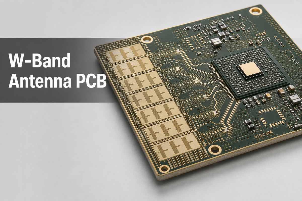
A W-band antenna PCB integrates, feeds, packages or interconnects an antenna system operating in the W-band, commonly treated as 75-110 GHz. At these frequencies, laminate behavior, copper geometry, registration, transitions, assembly and test fixtures can change electrical performance, so the board must be designed and manufactured as part of the RF system rather than as a conventional interconnect.
The right implementation may be an etched antenna, a phased array, a substrate-integrated waveguide (SIW) structure, an antenna-in-package interface or a hybrid PCB-to-waveguide assembly. There is no universal stackup or trace dimension for every project. Electrical models, mechanical interfaces, fabrication limits and validation methods must be agreed for the actual design.
What Is a W-Band Antenna PCB?
A W-band antenna PCB is a frequency-sensitive circuit structure in which the board participates directly in radiation, RF feeding, beamforming, packaging or transition to another transmission medium. Small dimensional changes that are harmless at lower frequencies can create measurable phase, loss or impedance differences in W-band channels.
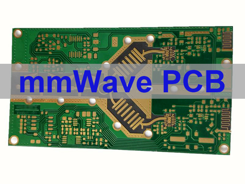
The term does not describe one fixed antenna shape. A PCB can carry a single radiating element, a corporate-feed network, a multi-channel array, SIW cavities, launch structures or the interface between a chipset and a waveguide antenna. A practical “mmwave pcb antenna” design therefore begins by defining which electromagnetic functions belong to the PCB and which belong to the package, connector, waveguide or surrounding enclosure.
W-band projects usually require closer coordination among antenna designers, package engineers, PCB fabricators, assemblers and test engineers. Their models must use compatible material assumptions, reference planes and mechanical dimensions; otherwise a board can meet its drawing yet miss the system target.
Where Are W-Band Antenna PCBs Commonly Used?
W-band antenna PCBs are used where compact antennas, short wavelengths, wide available bandwidth or fine angular resolution justify the added design and validation effort. The exact frequency allocation and product rules depend on the application and region, so the system specification should define the intended operating window.
Common engineering contexts include:
- short-range and multi-gigabit wireless links;
- imaging, sensing and research instruments;
- phased-array and beam-steering platforms;
- radar development above conventional automotive radar bands;
- frequency-extender, calibration and laboratory evaluation hardware;
- compact modules that transition between silicon, PCB and waveguide structures.
Which W-Band Antenna Type Is Best for Your PCB Project?
The best antenna type is the one that meets the radiation, bandwidth, packaging and manufacturing targets with a testable interface. A simple etched structure may reduce part count, while an array, SIW or antenna-in-package approach can better support gain, integration or feed control at the cost of added process sensitivity.
| Architecture | Typical fit | Main manufacturing concern |
| Etched patch or slot | Compact single element or small array | Etch geometry, copper profile, dielectric thickness and surrounding metal |
| Corporate-fed array | Higher gain or controlled beam pattern | Feed symmetry, cumulative phase error and registration across channels |
| SIW or PCB waveguide | Low-profile guided structures and transitions | Via placement, cavity dimensions, plating and launch repeatability |
| Antenna-in-package | Short chip-to-antenna path and dense integration | Package-to-board transition, assembly alignment and warpage |
| Hybrid PCB-to-waveguide | System connection to horn or metal waveguide | Mechanical datum, aperture alignment, surface contact and fixture repeatability |
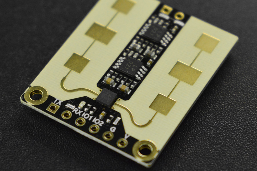
A “w band patch antenna” can be suitable when its bandwidth, gain and installation environment are compatible with a planar radiator. A “w-band antenna array” is more appropriate when the system needs higher effective aperture or beam steering, but the additional channels make material variation, conductor geometry and assembly alignment harder to control.
What Should Be Confirmed Before W-Band Antenna PCB Design?
Confirm the RF, mechanical, material and validation boundaries before committing the layout. The project should not begin with a generic 50-ohm trace assumption because the usable geometry depends on the transmission structure, laminate construction, copper profile and surrounding reference planes.
The design team should establish:
- operating frequency range, channel plan and required bandwidth;
- antenna architecture, polarization, gain and scan requirements;
- chipset, package, connector, waveguide and enclosure interfaces;
- material family, target dielectric properties and allowed construction options;
- stackup, copper profile, conductor definition and registration assumptions;
- simulation reference planes and de-embedding approach;
- acceptable amplitude, phase, impedance and radiation-pattern criteria;
- prototype quantity, assembly state and planned validation stages.
These inputs do not need to become a long document checklist. They need to be consistent. A model based on one dielectric thickness or copper treatment cannot reliably predict a board manufactured with another construction.
How Should a W-Band Antenna Be Placed and Routed on the PCB?
Place the antenna and its feed network as a controlled electromagnetic region, not as ordinary signal routing. Keep the layout consistent with the simulated stackup, reference planes, enclosure and launch geometry, and protect the antenna aperture from copper, components and mechanical features that were absent from the model.
Useful layout controls include:
- keeping feed paths short, geometrically consistent and free of unplanned neck-downs;
- preserving the intended ground return and avoiding reference-plane discontinuities;
- using symmetric routing where array channels require matched phase and amplitude;
- locating via fences and SIW rows from the electromagnetic design, not from a generic spacing rule;
- defining copper keepouts around radiating elements and transitions;
- placing mounting holes, shields, fasteners and enclosure walls in the simulation model;
- avoiding solder mask or surface treatments over critical RF regions unless the design explicitly includes them.
Via stitching can support ground continuity and field confinement, but more vias are not automatically better. Via diameter, pitch, antipad, plating and distance from the RF structure all affect the local field and manufacturability.
Which Materials and Stackups Affect W-Band Antenna Performance?
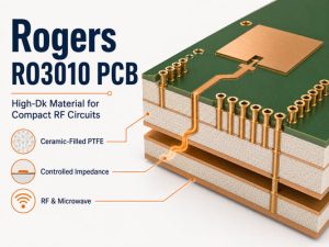
Materials and stackups affect W-band performance through dielectric constant, loss, thickness variation, moisture behavior, copper roughness, glass weave and construction repeatability. A material name alone is not enough; the design model should reflect the actual laminate, copper and fabrication construction being purchased.
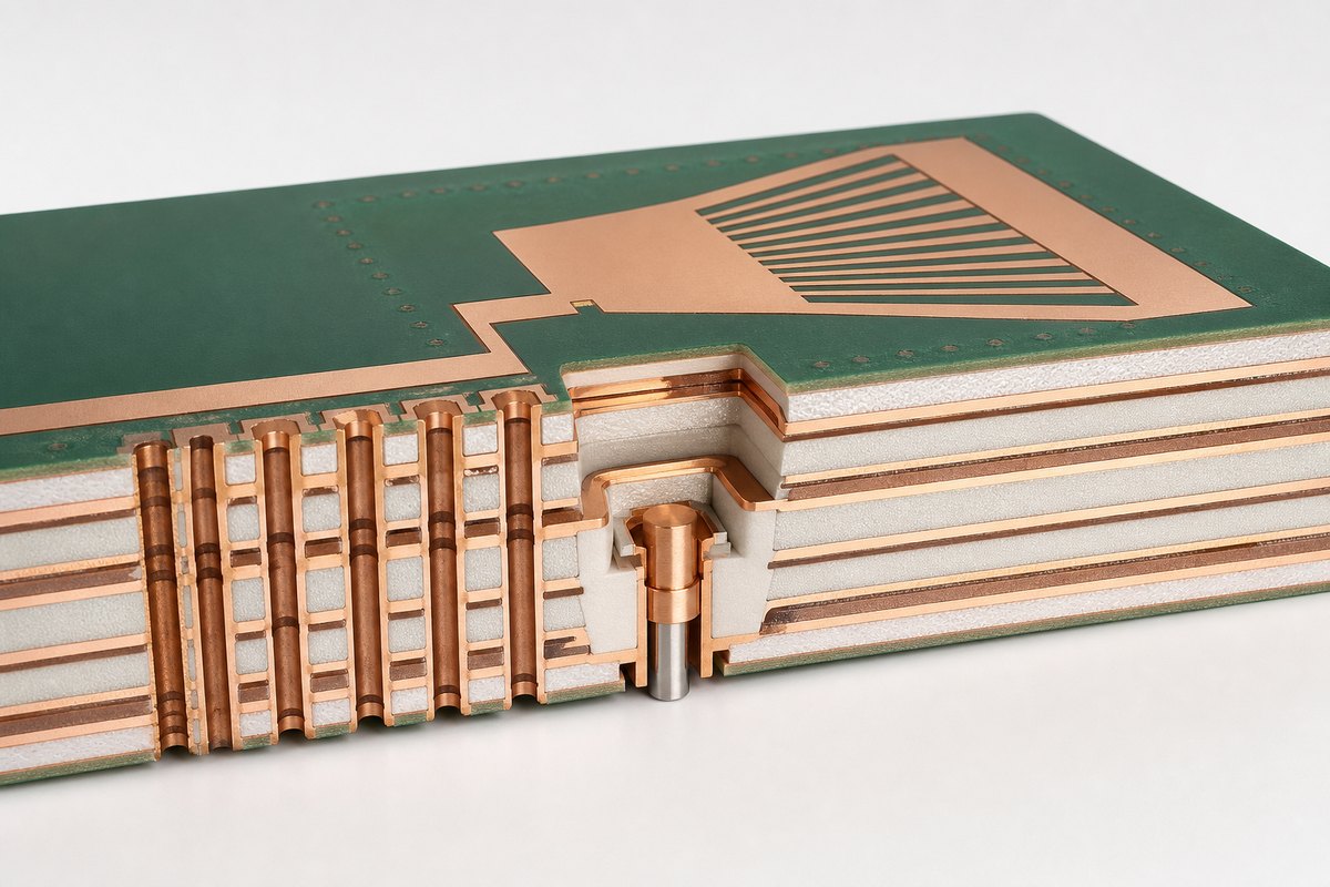
Review these variables together:
- design Dk and its test method at a relevant frequency;
- dissipation factor and conductor-loss assumptions;
- dielectric thickness and its manufacturing tolerance;
- copper foil type, profile and plated thickness;
- glass reinforcement or anisotropy when present;
- bondply, prepreg or adhesive behavior in a hybrid stackup;
- dimensional stability through lamination and subsequent thermal cycles;
- surface finish and solder mask interaction with exposed RF conductors.
Low nominal Df does not guarantee low insertion loss if rough copper, long feeds or poor transitions dominate. Likewise, two laminate constructions with similar datasheet Dk values may produce different effective impedance and phase when their reinforcement, resin content or copper profile differs. For a broader material context, see our RF Microwave PCB guide.
How Do Feed Lines, Impedance Matching, Vias and Transitions Affect Performance?
Feed lines and transitions determine how much of the generated W-band energy reaches the antenna with the intended amplitude and phase. The whole path must be modeled across launches, vias, package pads, cavities, connectors and waveguide interfaces; checking only a straight transmission-line coupon leaves the most sensitive discontinuities untested.
At W-band, a transition can add loss or resonance through a small pad, antipad, stub, air gap or registration shift. Channel-to-channel differences can also accumulate through small length and geometry variations. The design should therefore define the reference plane for every reported result and distinguish simulated antenna impedance from the impedance seen through the complete feed and fixture.
Impedance control PCB principles still apply, but a conventional coupon may not represent the antenna feed, via transition or package launch. Use dedicated test structures when the project needs to separate material, line, transition and fixture effects.
What Is the W-Band Antenna PCB Design and Manufacturing Process?
The process should connect electromagnetic design, fabrication engineering and staged verification so that production data preserve the modeled structure. The PCB fabricator should review the stackup and critical geometry before release, while the antenna designer retains responsibility for RF synthesis and system-level performance.

- Define the operating band, antenna architecture, interfaces and validation targets.
- Select a manufacturable material system and build the preliminary stackup.
- Simulate the antenna, feed network, transitions, package and nearby mechanical features.
- Add fabrication tolerances to sensitivity analysis instead of validating only nominal geometry.
- Complete PCB DFM review for conductor definition, registration, drilling, plating and lamination.
- Fabricate coupons or representative test structures with the prototype panel.
- Inspect the bare board before assembly and record actual stackup or dimensional results where required.
- Assemble with controlled alignment, reflow profile, flatness and handling conditions.
- Measure interconnect behavior and antenna performance using agreed reference planes.
- Correlate test results with the model before freezing the production build.
A useful “mmwave pcb design guide” must include this feedback loop. If the prototype fails, the team needs enough coupon, dimensional and fixture data to identify whether the cause is the antenna model, the feed path, fabrication variation, assembly or measurement setup.
Why Does a W-Band Antenna PCB Show High Loss, Weak Gain or Phase Error?
High loss, weak gain and phase error usually come from several interacting sources rather than one obvious defect. Diagnose the signal path in stages and compare nominally identical channels before changing the antenna geometry.
| Symptom | Likely cause group | First check |
| Higher insertion loss | Material loss, copper roughness, long feed or transition loss | Compare line and transition test structures before OTA testing |
| Resonance shifted | Dielectric thickness, effective Dk, etch geometry or nearby metal | Measure critical dimensions and confirm the built stackup |
| Weak or distorted pattern | Feed imbalance, enclosure interaction, assembly obstruction or fixture scattering | Repeat with the agreed mechanical configuration and calibration boundary |
| Channel phase spread | Line-length, weave, copper, registration or package variation | Compare matched channels through the same fixture and reference plane |
| Poor repeatability | Connector torque, waveguide alignment, contact, cable movement or calibration drift | Re-seat the fixture and run a repeatability study |
Do not tune the board from a single unverified measurement. First confirm calibration, fixture repeatability and reference-plane location. Then compare bare-board dimensions, material construction and assembly state against the model.
How Should a W-Band Antenna PCB Be Tested Before Production?
Test a W-band antenna PCB in layers: bare-board quality, RF interconnect behavior and over-the-air antenna performance answer different questions. A PCB supplier can verify fabrication features and agreed electrical structures, but antenna gain and radiation pattern require suitable W-band equipment, fixtures and an OTA method.
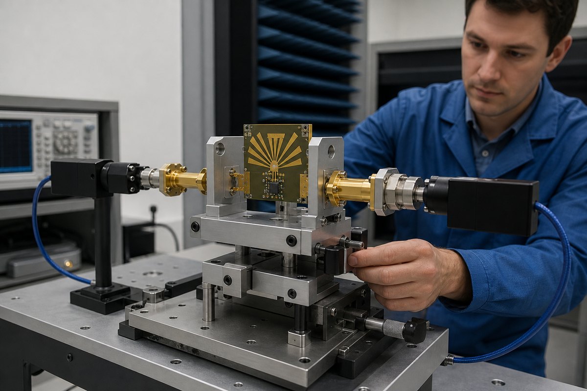
A practical validation sequence may include:
- visual and dimensional inspection of critical conductors, apertures and registration;
- microsection or construction verification for selected vias and layer relationships;
- continuity, isolation and agreed impedance or transmission-line coupons;
- line and transition measurements with defined calibration and de-embedding;
- channel-to-channel amplitude and phase comparison for arrays;
- assembled-module checks with the final package, connector or waveguide interface;
- OTA return loss, gain, pattern, polarization and scan testing when the responsible laboratory capability is confirmed.
W-band characterization commonly uses frequency extenders and waveguide hardware. Fixture design, flange alignment and calibration boundaries must be documented because a fixture error can look like a PCB or antenna defect.
How Do Assembly and Packaging Affect W-Band Antenna Performance?
Assembly and packaging affect W-band performance by changing alignment, standoff, flatness, local dielectric loading and transition geometry. A bare board that matches its drawing can still perform differently after a chipset, shield, radome, heat spreader or waveguide block is installed.
Control the assembly variables that are included in the RF model:
- package placement and rotation relative to feed structures;
- solder volume, collapse and standoff for flip-chip or fine-pitch interfaces;
- board and package warpage through reflow;
- underfill, adhesive or coating near active RF regions;
- connector or waveguide flange alignment and fastener sequence;
- shield, enclosure and absorber position;
- cleanliness and surface contamination around exposed conductors.
If assembly is outsourced separately from PCB fabrication, provide the assembler with the RF-sensitive keepouts and mechanical datums. Standard placement tolerances may not describe the relative alignment that the antenna transition actually needs.
What Factors Affect W-Band Antenna PCB Cost?
W-band antenna PCB cost is driven by material choice, stackup complexity, tolerance control, prototype learning and validation—not by board area alone. Early agreement on which characteristics are truly critical can prevent unnecessary controls while protecting RF performance.
The main cost drivers are:
- specialty laminate availability and minimum purchase quantities;
- hybrid or sequential lamination construction;
- thin dielectric layers and tight thickness control;
- fine conductor geometry, copper-profile requirements and etch compensation;
- registration demands across antenna, feed and via structures;
- small or dense plated holes, SIW rows and backdrilling when applicable;
- dedicated coupons, dimensional reports, microsections or RF test structures;
- assembly alignment, package complexity and special fixtures;
- prototype iterations needed to correlate simulation and measured results;
- production quantity, panel utilization and accepted yield window.
Cost should be reviewed against the validation plan. Removing a useful test structure may reduce initial panel cost but make a failed prototype harder to diagnose. Conversely, specifying a universal tight tolerance without sensitivity evidence can add cost without improving the antenna.
FAQ About W-Band Antenna PCB Projects
Is W-band always defined as 75-110 GHz?
75-110 GHz is a common engineering definition for the W-band, but applications, instruments and regulations may use narrower windows. State the exact operating range and channel plan in the project specification rather than relying only on the band name.
Can a w band patch antenna be fabricated as a conventional multilayer PCB?
It can use familiar PCB processes, but the construction may need tighter control of dielectric thickness, copper geometry, surface condition and registration than a conventional digital board. The antenna model must use the proposed stackup and manufacturing tolerances.
Which laminate properties matter most for a mmwave pcb antenna?
Design Dk, dissipation factor, thickness tolerance, copper roughness, reinforcement structure, moisture behavior and dimensional stability can all matter. Their relative importance depends on whether loss, phase consistency, resonance or mechanical stability dominates the design.
Does a PCB supplier validate antenna gain and radiation pattern?
Not automatically. A PCB supplier may inspect construction, dimensions and agreed RF coupons. Gain, radiation pattern, polarization and scan performance require suitable W-band fixtures and OTA equipment, so the responsible test party and acceptance method must be confirmed for each project.
What project information should be confirmed before production?
Confirm the operating range, antenna type, final stackup, named laminate, copper construction, critical geometry, mechanical interfaces, assembly state, quantity and acceptance method. Provide Gerber or ODB++ data plus relevant package or waveguide drawings when they are part of the manufactured interface.
Why can nominally identical antenna channels show different phase or gain?
Small differences in feed length, dielectric construction, glass weave, copper profile, registration, package alignment or fixture contact can accumulate across channels. Compare the channels through the same calibrated setup and inspect actual geometry before changing the design.
How Can EBest Circuit Support Your W-Band Antenna PCB Project?
EBest Circuit supports RF and high-frequency PCB manufacturing, impedance-controlled PCB work, impedance testing and engineering review for available high-frequency material systems. Because W-band performance depends on the exact stackup, copper construction, antenna topology, transitions and validation method, we review each design for manufacturability and sourcing feasibility rather than promise one universal process window.
Send the target frequency range, antenna architecture, Gerber or ODB++ data, stackup, material and copper requirements, critical tolerances, package or waveguide interface drawings, assembly information, quantity and RF acceptance plan to our engineering team at sales@bestpcbs.com. We can review the PCB manufacturing and assembly scope with your team. Antenna synthesis, W-band VNA measurement and OTA gain or pattern validation are included only when the responsible capability is confirmed for the specific project.