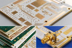
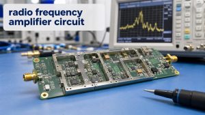
An RF transceiver PCB prototype may work perfectly in the lab but fail to deliver consistent performance in mass production. Small variations in trace impedance, RF matching components, solder joints, or grounding can affect transmission power and receiver sensitivity. These problems become more expensive to address once production begins.
Moving an RF transceiver PCB from prototype to mass production requires more than successful RF testing. Material selection, DFM review, precise SMT assembly, component availability, and repeatable inspection must all be considered. This guide covers the manufacturing and assembly requirements that help OEM teams reduce production risks, control costs, and prepare wireless products for volume manufacturing.
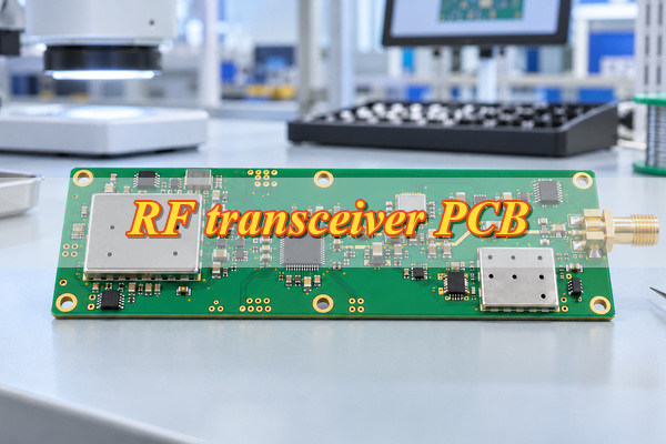
What Is an RF Transceiver PCB?
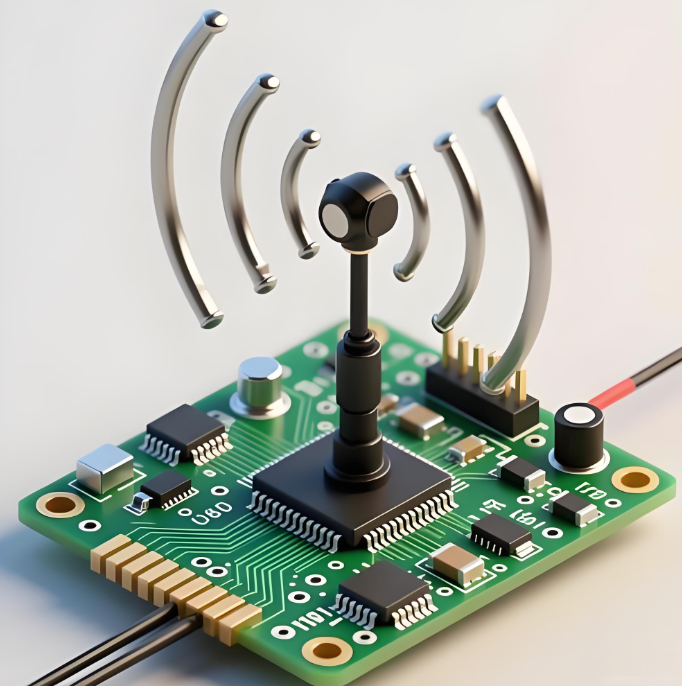
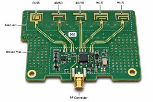
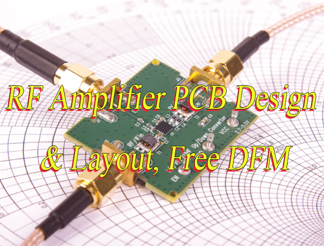
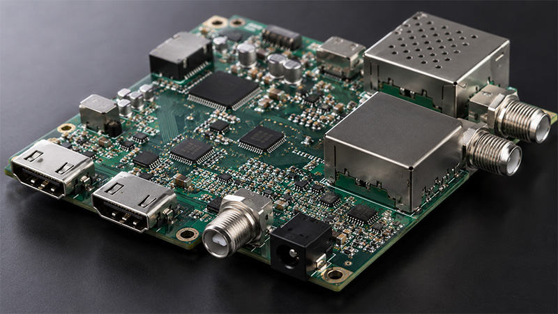
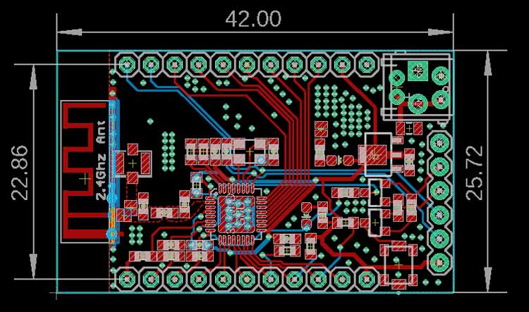
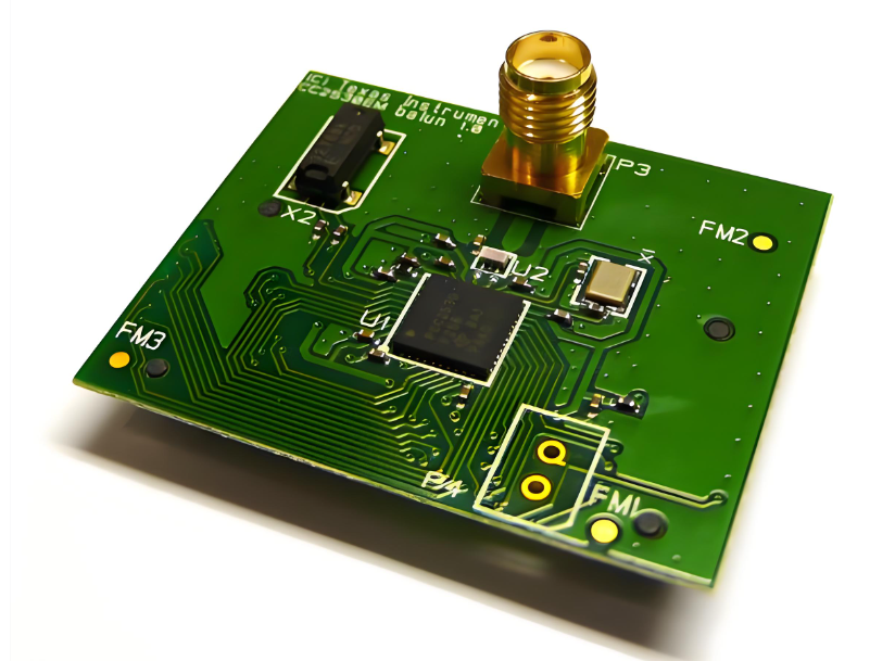
An RF transceiver PCB is a printed circuit board that integrates radio‑frequency transmitting and receiving circuits for wireless communication. It typically combines an RF transceiver IC, matching networks, filtering, power management, and antenna connections.
RF transceiver PCBs are used in industrial wireless controls, IoT gateways, telemetry equipment, wireless sensors, and communication terminals. Depending on the design, they may support frequencies such as 433 MHz, 868 MHz, 915 MHz, or 2.4 GHz.
An RF transceiver IC performs the core radio functions, while an RF module integrates the IC with supporting circuitry into a packaged subsystem. A complete RF transceiver PCB may also include processing, power regulation, external interfaces, and additional RF components.
Unlike an optical transceiver PCB, an RF transceiver PCB handles radio‑frequency electrical signals for wireless communication.
What Components Are Used on an RF Transceiver PCB?
The components on an RF transceiver PCB depend on its operating frequency, transmission power, receiver sensitivity, and wireless architecture. Some designs integrate most radio functions into one IC, while others use separate RF front‑end components.
| Component | Function | Assembly Consideration |
|---|---|---|
| RF Transceiver IC | Transmits and receives RF signals | QFN/BGA alignment, grounding |
| Power Amplifier (PA) | Increases transmit output power | Thermal pad soldering, heat dissipation |
| Low‑Noise Amplifier (LNA) | Amplifies weak received signals | Grounding, component placement |
| RF Filters | Suppress unwanted frequencies | Correct part number, solder quality |
| RF Switch | Routes transmit/receive signals | Placement and RF connections |
| Matching Components | Adjust RF impedance | Accurate L/C values, small SMT packages |
| Crystal Oscillator | Provides frequency reference | Placement, mechanical stability |
| Power Management IC | Regulates supply voltages | Decoupling, thermal performance |
| MCU / Processor | Manages communication and control | Digital signal isolation |
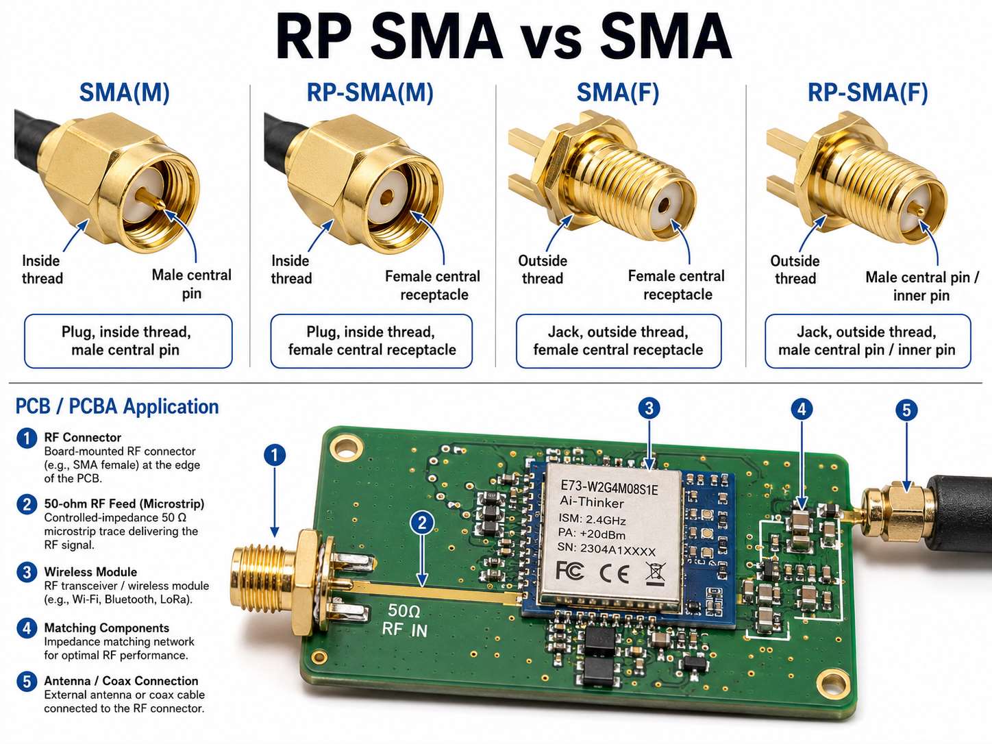
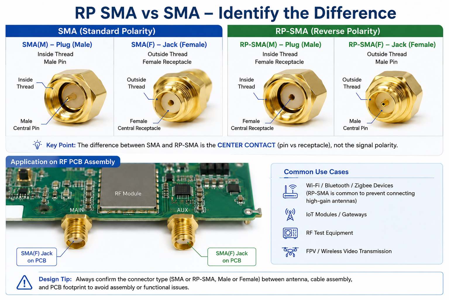
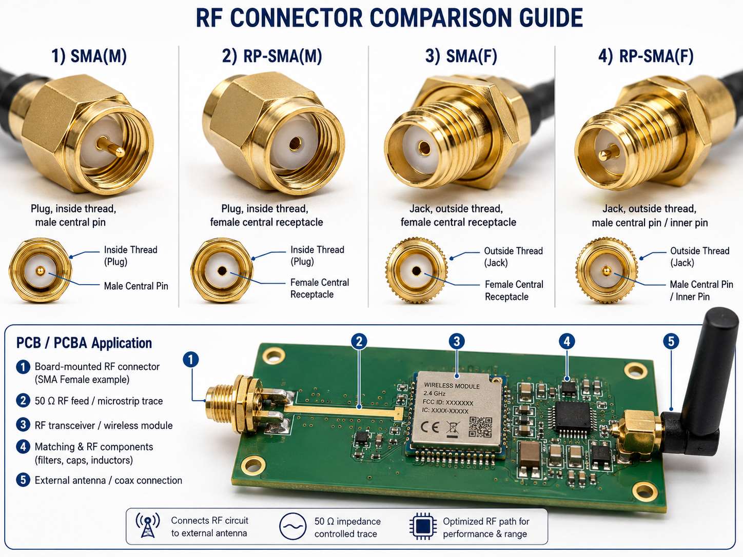
| RF Connector | Connects antennas or test equipment | Mechanical alignment, grounding |
Not every design requires separate PA, LNA, or RF switch components. These functions may be integrated into the transceiver IC or RF front‑end module.
For assembly, RF matching components, exposed thermal pads, fine‑pitch ICs, and antenna connectors deserve particular attention. Component substitutions or placement variations can change RF performance even when basic electrical tests pass.
What Should You Check in an RF Transceiver PCB Design?
Before manufacturing an RF transceiver PCB, check whether its stackup, RF routing, component footprints, and thermal structures can be produced consistently. A design that works in simulation may still require manufacturing adjustments to meet the specified tolerances.
The following areas should be reviewed before prototype fabrication:
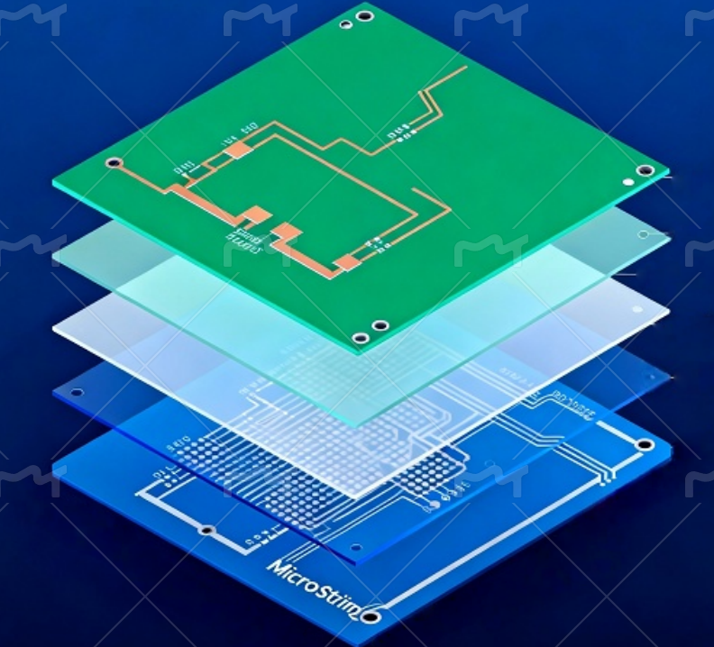
- PCB Materials and Stackup: Select FR-4 or low‑loss materials based on operating frequency, allowable insertion loss, and dielectric properties. Confirm dielectric thickness, copper weight, and reference‑plane locations.
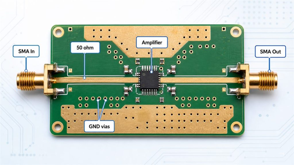
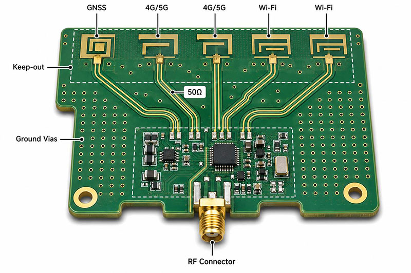
- RF Trace Impedance: Verify the specified transmission‑line impedance, commonly 50 ohms for many antenna‑feed structures. Review trace width, spacing, copper thickness, and manufacturing tolerances.
- Grounding and Shielding: Maintain suitable RF return paths, ground‑via connections, and shield‑can footprints. Follow antenna clearance and grounding requirements from the RF device reference design.
- RF Component Layout: Check matching‑network placement, QFN/BGA footprints, exposed pads, and nearby via structures. Unnecessary changes to a qualified RF reference layout may affect matching and harmonic performance.
- PA Thermal Management: Review thermal pad dimensions, heat‑transfer vias, and copper areas against the device’s thermal requirements.
- RF Connector Installation: Confirm connector footprint dimensions, edge clearances, ground connections, and mechanical support.
- SMT Manufacturability: Check small passive component spacing, solder‑mask clearances, assembly orientation, and test‑point accessibility.
FR-4 is not automatically unsuitable for RF transceivers. Its suitability depends on frequency, trace length, insertion‑loss limits, and material properties. Low‑loss laminates become more attractive when ordinary FR-4 cannot meet the RF performance budget.
A DFM review should identify fabrication and assembly concerns before tooling and material preparation. It does not replace the customer’s RF circuit design or performance validation.
How Are RF Transceiver PCB Prototypes Manufactured and Assembled?
RF transceiver PCB prototyping combines controlled PCB fabrication with accurate assembly of RF and digital components. The objective is to produce a prototype that represents the intended manufacturing specifications.
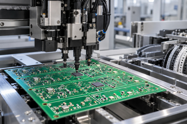
Step 1: PCB Fabrication
Fabrication includes material preparation, imaging, etching, lamination, drilling, copper plating, solder‑mask application, and surface finishing.
For RF transceiver PCBs, particular attention goes to controlled trace geometry, dielectric thickness, layer alignment, and plated‑through‑hole quality. These affect transmission‑line impedance and interconnect consistency.
Step 2: Solder Paste Printing and SMT Placement
Solder paste is applied through a stencil, followed by placement of RF ICs, matching components, filters, oscillators, and supporting circuitry.
Small inductors and capacitors require accurate placement and the correct component values. QFN and BGA packages also require suitable stencil apertures, placement accuracy, and thermal profiles.
Step 3: Reflow Soldering and Additional Assembly
Components are soldered using a controlled reflow process. Through‑hole components, coaxial connectors, and other mechanical parts are assembled as specified.
Shielding cans may be installed using a suitable soldering process, depending on their design and whether access is required for subsequent inspection or RF tuning.
Step 4: Assembly Inspection
The assembled prototype is inspected for solder defects, component alignment, polarity, and connector installation.
RF matching components and QFN ground connections deserve additional inspection attention, as defects in these areas can affect RF performance without necessarily causing a complete electrical failure.
How Are RF Transceiver PCB Prototypes Inspected and Tested?
RF transceiver PCB testing should separate manufacturing defects from actual radio‑performance problems. A board that powers on successfully has not necessarily passed RF verification.
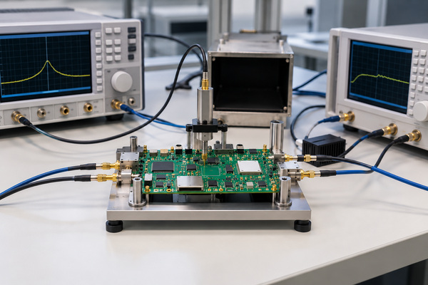
Testing is typically divided into three stages.
| Test Stage | Typical Checks | Purpose |
|---|---|---|
| Bare PCB | Electrical continuity, shorts, controlled impedance | Verify PCB fabrication |
| PCB Assembly | SPI, AOI, X‑Ray where applicable | Detect placement and solder defects |
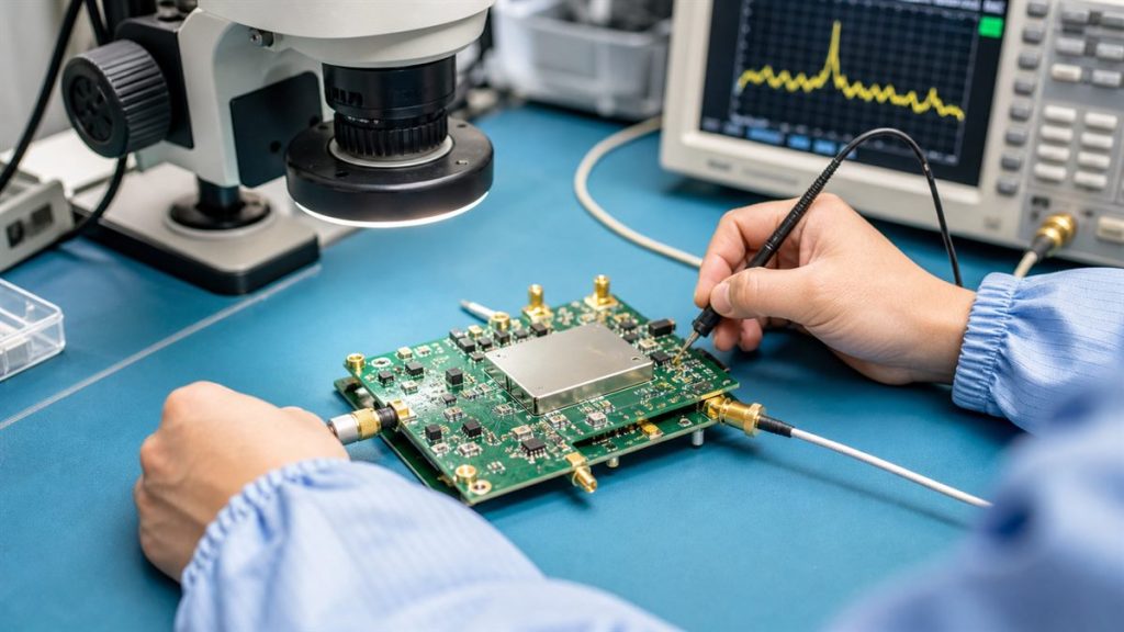
| RF Function | TX power, RX sensitivity, frequency accuracy, spectrum, communication | Verify radio performance |
The required inspections depend on the customer’s specifications, device architecture, and available test equipment.
For RF functional verification, common measurements include:
- Transmit Power: Check conducted output power against the specified operating conditions.
- Receiver Sensitivity: Confirm reception performance at defined input levels, data rates, and error‑rate limits.
- Frequency Accuracy: Verify oscillator‑related frequency error within the device requirements.
- Spectrum and Harmonics: Examine unwanted emissions and occupied signal characteristics.
- Communication Test: Confirm packet transmission and reception using the intended protocol and test setup.
RF testing should also consider the antenna configuration and whether measurements are conducted through a connector or performed over the air.
Antenna matching and enclosure effects may require validation on the completed product, not just the bare PCBA.
RF functional testing is not automatically included in every PCB assembly order. The customer and manufacturer should agree on test fixtures, firmware, procedures, measurement equipment, and acceptance criteria before production.
What Must Be Confirmed Before RF Transceiver PCB Mass Production?
A successful prototype does not automatically mean an RF transceiver PCB is ready for mass production. The next step is to confirm that the approved design, materials, assembly process, and inspection requirements can be reproduced at the required quantity.
Before releasing the project for volume manufacturing, confirm:
- Approved PCB Revision: Finalize fabrication files, stackup, impedance requirements, and material specifications. Any change affecting the RF path should be reviewed.
- BOM and Component Availability: Verify RF transceiver ICs, filters, oscillators, matching components, and approved sourcing channels. Restrict substitutions where electrical or RF characteristics must remain unchanged.
- Assembly Process: Confirm solder paste requirements, critical component placement, reflow profiles, shield installation, and connector assembly.
- RF Performance Limits: Establish approved transmit power, receiver sensitivity, frequency accuracy, and other applicable performance thresholds.
- Test Fixtures and Procedures: Confirm the required test equipment, test coverage, firmware version, sampling method, and acceptance criteria.
- Pilot Production: Use a pre‑production build to evaluate assembly yield, process stability, and manufacturing consistency before scaling up.
- Change Control: Maintain approved PCB, BOM, firmware, and test‑document revisions so that production changes remain traceable.
The most expensive production problems often come from changes that were not evaluated against the approved prototype.
A controlled pilot build helps reveal manufacturing variation before it affects a full production batch.
How Can You Maintain Consistent RF Performance in Mass Production?
Consistent RF performance depends on controlling fabrication, component sourcing, assembly, and inspection across production batches. Small changes in materials or component characteristics may affect wireless performance even when the PCB layout remains unchanged.
The main production controls include:
- PCB Fabrication Consistency: Control specified trace dimensions, dielectric thickness, copper plating, and layer registration to maintain the approved transmission‑line geometry.
- SMT Process Control: Monitor solder paste printing, component placement, and reflow conditions, particularly around RF ICs, small matching components, and thermal pads.
- Component Lot Control: Verify part numbers and approved substitutions for RF filters, amplifiers, oscillators, and matching components. Maintain the required lot records.
- Inspection and Test Consistency: Apply the approved inspection plan and relevant functional tests using controlled procedures and calibrated equipment.
- Production Traceability: Link PCB and component lots with assembly records, inspection results, test data, and approved revisions.
A common risk is assuming that two electrically compatible RF components will produce identical RF behavior. Differences in tolerance, parasitic characteristics, or frequency response can affect matching and filtering.
Where applicable, use agreed workmanship and soldering requirements such as IPC‑A-610 and IPC J‑STD-001, together with project‑specific RF acceptance criteria.
What Affects RF Transceiver PCB Cost and Lead Time?
RF transceiver PCB manufacturing cost and delivery time depend on PCB complexity, RF component availability, assembly requirements, testing scope, and order quantity.
| Cost Factor | Main Impact | Practical Consideration |
|---|---|---|
| PCB Material | Material price and availability | Select according to RF loss requirements |
| Layer Count and Stackup | Fabrication complexity | Avoid unnecessary layers |
| Impedance Tolerance | Process control and verification | Specify realistic tolerances |
| RF Component Supply | BOM cost and procurement time | Confirm availability before release |
| QFN/BGA Assembly | SMT process and inspection | Provide complete assembly data |
| RF Shielding and Connectors | Additional materials and operations | Finalize specifications early |
| RF Testing | Fixtures, equipment, test time | Define test scope before quotation |
| Order Quantity | Setup and unit economics | Plan prototype and production quantities |
Low‑loss laminates may increase material and fabrication costs, but using them where the design does not require their properties adds unnecessary expense.
Similarly, late BOM changes, unapproved component substitutions, and undefined RF test requirements can delay production.
For more reliable quotations, provide the expected prototype quantity, planned production volume, component sourcing requirements, and test specification together.
Why Choose EBest Circuit for RF Transceiver PCB Manufacturing and Assembly?
EBest Circuit provides PCB fabrication, component sourcing support, and PCB assembly services for RF transceiver projects, from initial prototypes to volume production. Our manufacturing reviews focus on producing customer‑provided designs to agreed specifications while identifying potential production risks.
Our services help customers in the following areas:
- Reduce Supplier Coordination: Combine custom PCB manufacturing, SMT assembly, through‑hole assembly, and relevant inspection requirements with one manufacturing partner.
- Identify Manufacturing Risks Early: Receive DFM guidance on stackups, tolerances, component footprints, thermal pads, and assembly feasibility before production.
- Support RF Component Procurement: Review BOM availability and sourcing requirements to reduce disruption from shortages or unapproved substitutions.
- Simplify Prototype‑to‑Production Transfer: Coordinate approved PCB revisions, component specifications, and assembly requirements across different production stages.
- Maintain Quality Visibility: Support agreed inspection requirements, material records, and up to 15 years of production traceability.
- Access Dedicated Technical Support: Every EBest PCBA project is supported by a 1+3 technical team consisting of PE, DFM, Process, and Quality personnel.
EBest Circuit operates as a PCB and PCBA manufacturer, providing DFM technical guidance and manufacturing reviews rather than original RF circuit design.
For RF transceiver projects requiring specialized functional testing, we review the customer‑provided test requirements to determine suitable manufacturing and verification arrangements before accepting the order.
What Information Do You Need for an RF Transceiver PCB Quote?
A complete RF transceiver PCB RFQ should include both fabrication and assembly requirements. Missing RF specifications or component information can delay the quotation and manufacturing review.
Please provide:
- PCB Manufacturing Files: Gerber or ODB++ files, drill data, board dimensions, and fabrication drawings.
- PCB Specifications: Layer count, stackup, material preferences, copper thickness, and controlled‑impedance requirements.
- Bill of Materials: Component part numbers, quantities, manufacturers, and substitution restrictions.
- Assembly Files: Pick‑and‑place data, assembly drawings, polarity information, and special assembly instructions.
- RF Requirements: Operating frequency, antenna and RF connector specifications, shielding details, and critical RF acceptance limits.
- Production Quantity: Prototype quantity, pilot‑build quantity, and expected volume production demand.
- Testing Requirements: Required inspection methods, functional‑test procedures, fixtures, firmware, and acceptance criteria.
- Delivery Requirements: Requested schedule, delivery destination, and any applicable packaging instructions.
Send your RF transceiver PCB files and RFQ to sales@bestpcbs.com. EBest Circuit can review the manufacturing requirements, clarify technical details, and prepare a quotation based on the approved project scope.
FAQs About RF Transceiver PCBs
Q1: Can one RF transceiver use the same antenna for transmitting and receiving?
A1: Yes. Many transceivers share one antenna through an integrated or external TX/RX switch, duplexer, or other suitable RF network. The arrangement depends on the operating bands and whether transmission and reception occur simultaneously.
Q2: Do all RF transceiver boards require a power amplifier?
A2: No. Some transceiver ICs provide sufficient output power without an external PA. Higher‑power or longer‑range applications may use an additional amplifier, subject to power, thermal, and regulatory limits.
Q3: Can an RF transceiver PCB support multiple frequency bands?
A3: Yes, if the transceiver IC and RF front end support those frequencies. Filters, matching networks, switches, and antennas must also be suitable for the required bands.
Q4: Does an RF transceiver always require a shielding can?
A4: No. Shielding depends on RF sensitivity, component layout, interference sources, and enclosure conditions. Good grounding and layout remain essential, whether or not a shielding can is installed.
Q5: Can an RF transceiver IC and MCU be placed on the same PCB?
A5: Yes. Integrated RF and digital designs are common. Careful grounding, supply decoupling, and isolation of noisy digital signals help prevent interference with sensitive RF circuits.
Q6: Does a certified RF module eliminate final‑product certification requirements?
A6: No. Module approval may simplify some requirements, but the finished product can still require evaluation depending on antenna changes, installation conditions, additional transmitters, and applicable regulations.
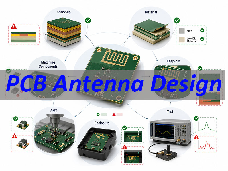
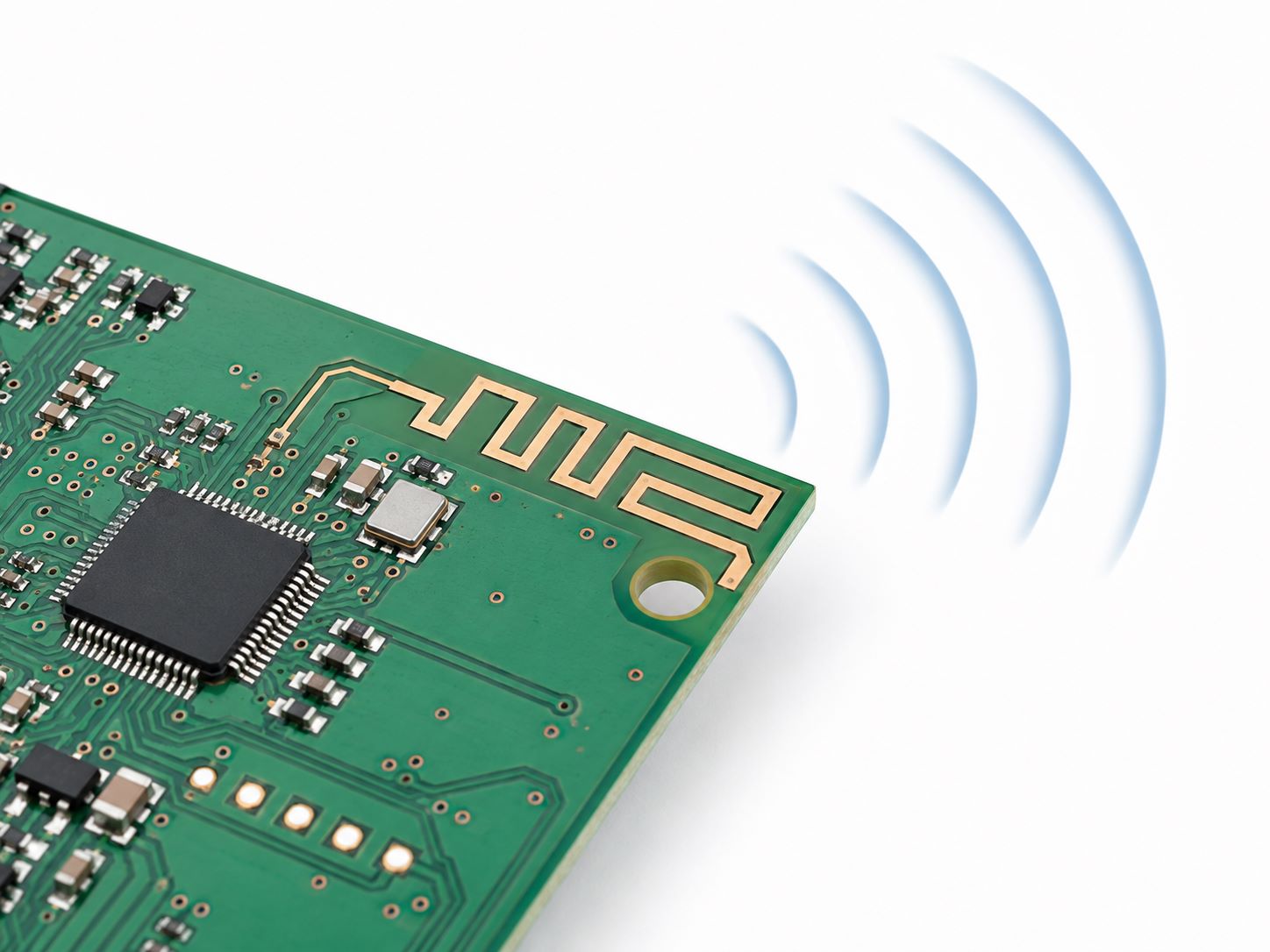
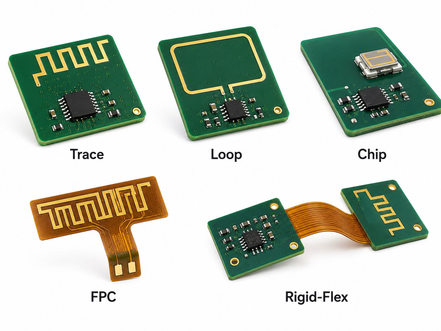
Q7: Can an RF transceiver PCB use an integrated PCB antenna?
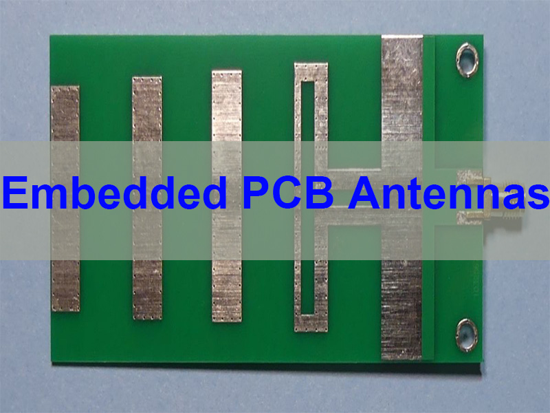
A7: Yes. PCB antennas can eliminate external antenna connectors in suitable designs. However, antenna geometry, ground clearance, enclosure materials, and final‑product matching must be considered.
Q8: Can customer‑supplied RF components be used for PCB assembly?
A8: Yes, subject to manufacturing agreement and component verification. Customers should provide approved part numbers, quantities, packaging information, and handling requirements, particularly for moisture‑sensitive or traceability‑controlled components.
Q9: Does antenna matching have to be verified after PCB assembly?
A9: It is recommended when the antenna, RF layout, enclosure, or nearby components affect matching. Final‑product RF validation can reveal performance differences not visible during bare PCB inspection.
Q10: Can RF matching components be adjusted during prototype validation?
A10: Yes. Authorized RF engineers may tune matching networks based on measured performance. Approved component values and BOM revisions must be documented before pilot or volume production.
Conclusion
Successful RF transceiver PCB production depends on more than a working prototype. Controlled impedance, accurate RF component assembly, verified performance, approved materials, and repeatable quality controls all contribute to consistent results. Confirming these requirements before mass production helps reduce unexpected manufacturing changes, component delays, and quality risks.
Ready to move your RF transceiver PCB from prototype to mass production? EBest Circuit provides custom PCB manufacturing, SMT and mixed assembly, DFM technical guidance, and volume production support. Send your Gerber files, BOM, assembly requirements, and production quantities to sales@bestpcbs.com for a technical review and quotation.