PCB manufacturing PCB manufacturing
Home > Blog

RF Microwave PCB

RF Microwave PCB: Design, Materials, Fabrication, and Manufacturer Guide
Thursday, May 21st, 2026

How can an RF microwave PCB keep high-frequency signals stable when small design and fabrication changes may affect the final result? This guide explains how RF microwave PCB boards work, how to choose suitable materials, how to control impedance and signal loss, and how to select the right manufacturer for prototype and production projects.

EBest Circuit (Best Technology) is an engineering-driven PCB and PCBA manufacturer with over 20 years of experience supporting high-frequency, RF, microwave, automotive, medical, industrial, communication, and aerospace/UAV projects. With self-owned PCB and PCBA factories, EBest provides DFM review, material selection support, controlled impedance PCB fabrication, component sourcing, assembly, testing, and production-quality support from prototype to mass production.

If you are evaluating an RF microwave PCB project and need practical manufacturing feedback, you can send your Gerber files, stackup, material requirements, and quantity to sales@bestpcbs.com for a technical review and quotation.
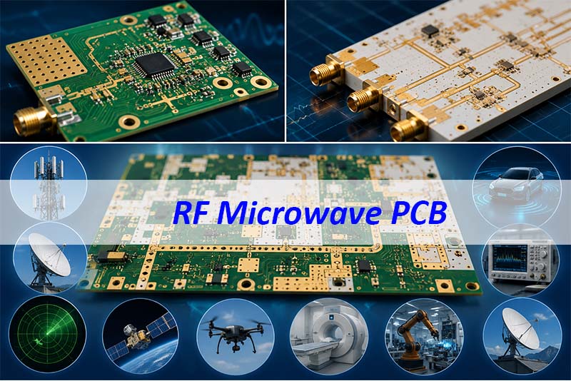
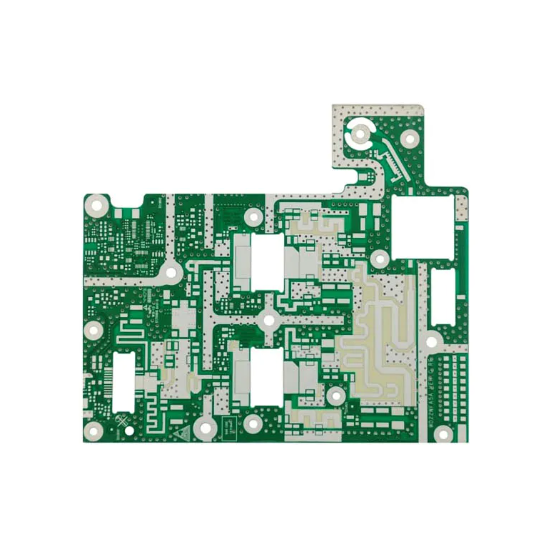
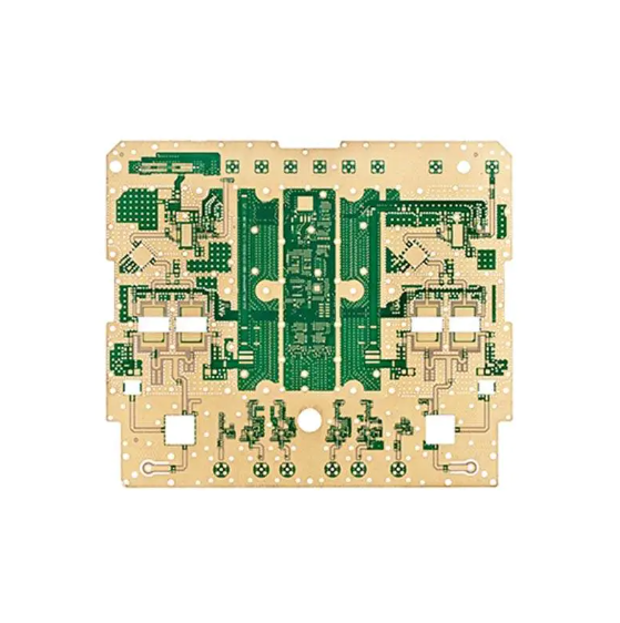
RF Microwave PCB

What Is an RF Microwave PCB Board?

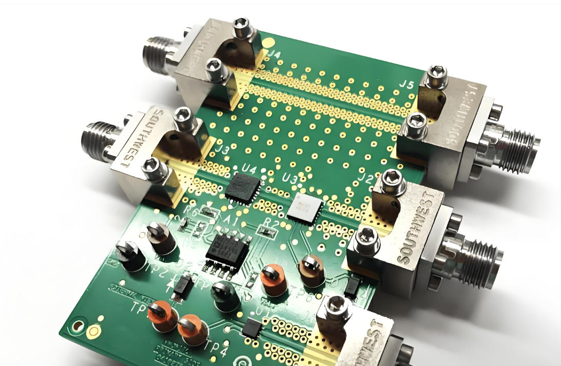
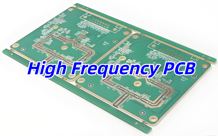
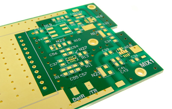
An RF microwave PCB board is a printed circuit board made for radio frequency and microwave signals. It is a high-frequency circuit board designed for RF and microwave signal transmission, usually covering applications from MHz-level RF circuits to GHz and millimeter-wave systems.

In simple terms, RF board PCB is a broader category for radio-frequency circuits, microwave PCB usually refers to higher-frequency GHz-range circuits, and RF microwave PCB board is often used to describe a low-loss, impedance-controlled PCB built for both RF and microwave performance.

Unlike a standard FR4 PCB, an RF microwave PCB is part of the signal path. Therefore, the board does more than connect components. It also affects signal speed, loss, phase, reflection, and radiation.

In many low-speed PCB designs, small material changes may not create serious issues. However, RF and microwave circuits are more sensitive. A small shift in dielectric thickness, copper roughness, or trace width can change the final electrical behavior.

RF microwave PCB boards are commonly used in:

  • 5G communication modules
  • RF antennas
  • Radar systems
  • Satellite communication equipment
  • Aerospace and UAV electronics
  • Industrial RF systems
  • Medical RF devices
  • Automotive radar and sensing modules
  • High-frequency test instruments
RF Microwave PCB

As a result, RF microwave PCB design must start with clear electrical goals. These goals may include low insertion loss, stable impedance, low return loss, strong grounding, and repeatable batch performance.

A well-built RF microwave PCB helps engineers reduce signal loss and improve circuit stability. It also makes the product easier to move from prototype to mass production.

How Does an RF Microwave High-Frequency PCB Work?

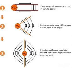
An RF microwave high-frequency PCB works by guiding electromagnetic energy through controlled signal paths. These paths may include microstrip lines, stripline traces, coplanar waveguides, grounded coplanar waveguides, and antenna feed lines.

At high frequencies, a copper trace is not just a simple wire. Instead, it works as a transmission line. The signal travels through both the copper and the surrounding dielectric field. Because of this, the material, trace width, spacing, ground plane, and via structure all affect performance.

Several factors matter most.

  • Impedance control is one of the first concerns. Many RF circuits use 50 ohm impedance, although some designs use other values. The final impedance depends on trace width, copper thickness, dielectric thickness, and dielectric constant.
  • Insertion loss is also important. It shows how much signal power is lost as the signal moves through the board. Loss can come from the dielectric material, copper surface, radiation, and poor transitions.
  • Return loss shows how much signal reflects back. Poor layout, sudden trace width changes, bad via design, or weak connector launch design may increase reflection.
  • Phase stability matters in radar, antenna, and communication systems. If the material or process changes too much, phase behavior may shift. This can affect signal timing and accuracy.
  • Ground return path is another key factor. RF current needs a clean return path. Therefore, a continuous ground plane and proper via stitching can help reduce noise, coupling, and radiation.

In short, an RF microwave PCB works well when the signal sees a stable path from the source to the load. Good design creates that path. Good fabrication keeps it consistent.

Where Are RF Microwave PCB Boards Used in 24GHz, 5G, and High-Power Applications?

RF microwave PCB boards are used in products where frequency, bandwidth, signal loss, and stability matter. Some boards are small antenna modules. Others are complex multilayer boards for communication systems.

Application AreaTypical RequirementPCB Focus
24GHz radarStable detection and low signal driftLow-loss laminate, precise impedance, antenna accuracy
5G RF modulesHigh bandwidth and stable transferStable Dk/Df, fine-line control, hybrid stackup
RF antennasGood radiation efficiencyAntenna geometry, copper tolerance, surface finish
Base stationsLong-term signal reliabilityThermal control, material consistency, multilayer control
Aerospace and UAVLightweight and stable RF performanceTraceability, process control, vibration resistance
Industrial RF equipmentReliable field operationStrong structure, thermal reliability, test control
High-power RF modulesHeat control and signal stabilityMetal-backed structure, thermal path, copper control
  • For a 24GHz RF microwave PCB, material choice and layout precision are already important. As the frequency rises, small geometry changes become more visible in actual RF performance.
  • For 5G-ready RF microwave high-frequency PCB fabrication, engineers often need low transmission loss, stable dielectric properties, and repeatable production. In many cases, they also need hybrid stackups. These stackups combine RF materials with FR4 or other support layers.
  • Meanwhile, high-power RF applications add another challenge: heat. These boards may need metal-backed structures, thermal vias, heavy copper areas, or a dedicated heat path.

Therefore, the best RF microwave PCB is not always the most complex board. It is the board that fits the signal, thermal, mechanical, and production needs of the product.

How to Do PCB Material Selection for RF Microwave Millimeter-Wave Design?

Material selection is one of the most important steps in RF microwave PCB design. The laminate affects signal loss, impedance, phase stability, heat control, and long-term reliability.

For PCB material selection for RF microwave millimeter-wave design, engineers usually check several material properties.

Material FactorWhy It Matters
Dielectric constant, DkAffects trace width, impedance, wavelength, and phase speed
Dissipation factor, DfAffects dielectric loss, especially at high frequency
Copper roughnessAffects conductor loss and signal attenuation
Thermal conductivityHelps move heat away from RF power areas
CTEAffects dimensional stability and via reliability
Moisture absorptionAffects dielectric stability and long-term use
Process compatibilityAffects drilling, lamination, routing, and yield

Common RF microwave PCB materials include Rogers high-frequency laminates, PTFE-based laminates, ceramic-filled hydrocarbon materials, Taconic materials, and other low-loss substrates.

However, the lowest-loss material is not always the best choice. The project may also need cost control, easy sourcing, stable production, and strong mechanical performance. Therefore, engineers should choose the material based on frequency, loss target, thermal need, stackup, volume, and budget.

In some projects, a hybrid stackup is a practical choice. For example, the RF layer may use a low-loss material, while the support layers use FR4. This helps reduce cost while keeping the high-frequency path stable.

Before production, the material choice should be reviewed with the manufacturer. This can help avoid problems with drilling, lamination, copper control, and dimensional stability.

What Are the Main RF Microwave PCB Board Design and Layout Rules?

Good RF microwave PCB board design and layout starts with a clean signal path. The layout should reduce loss, avoid sudden impedance changes, and give RF signals a stable return path.

Here are the main design rules.

Keep RF traces short and direct.

  • Shorter traces reduce loss and lower the risk of unwanted coupling. Also, avoid unnecessary stubs, long detours, and sharp changes in direction.

Control impedance from the start.

  • The stackup, copper thickness, dielectric thickness, and trace width should be planned before layout. This helps avoid later redesign.

Use a continuous ground plane.

  • A broken ground plane can disturb the return path. As a result, it may increase radiation and impedance mismatch.

Add ground via stitching where needed.

  • Ground vias near RF traces can help control the electromagnetic field. They can also reduce coupling between nearby circuits.

Pay attention to via transitions.

  • At high frequency, a via can create unwanted inductance and capacitance. Therefore, via size, pad size, anti-pad size, and via depth should be reviewed.

Separate noisy circuits from RF areas.

  • Power converters, digital clocks, and fast switching signals should stay away from sensitive RF paths. In addition, proper shielding and layer planning can reduce noise.

Review solder mask over RF traces.

  • Solder mask can change impedance because it adds material above the copper. Some RF designs need solder mask clearance over controlled traces.

Design connector launches carefully.

  • A poor RF connector launch can create reflection and loss. Therefore, the launch area should match the connector type, stackup, and target impedance.

Overall, RF layout is not only about routing traces. It is about building a stable electrical environment around each signal path.

What Pain Points Come With RF Microwave PCB, and How Does EBest Solve Them?

RF microwave PCB projects often face issues that are not obvious at first. A board may look correct, but still fail RF testing. Therefore, early review and stable fabrication control are important.

Customer ChallengeWhat Usually HappensHow EBest Supports the Project
Material choice is unclearThe customer knows the frequency, but not the best laminateEBest reviews frequency, Dk/Df, stackup, heat, cost, and production volume before giving material suggestions
Impedance is hard to controlSmall trace or dielectric changes may cause reflectionEBest supports controlled impedance fabrication and checks stackup, trace width, copper thickness, and impedance targets before production
Prototype results are hard to repeatThe first sample may work, but later batches may shiftEBest helps control material batches, etching, lamination, inspection, and process records
Hybrid stackups create process riskRF material and FR4 may behave differently during laminationEBest reviews hybrid stackup feasibility and gives DFM suggestions before fabrication
RF designs need PCB and assembly supportCustomers may need bare boards, components, assembly, and testingEBest provides PCB fabrication, component sourcing, PCBA assembly, and testing support under one workflow
Design files are not production-readySmall layout issues may lead to delay or reworkEBest provides DFM pre-review to help customers find risks before the board enters production

This structure keeps the problem and solution clear. It also helps buyers quickly see whether the manufacturer can support real project risks.

For RF microwave PCB projects, EBest does not only build boards from files. Instead, the engineering team can help review the practical manufacturing side of the design. This includes material selection, stackup, impedance control, trace tolerance, via design, and assembly needs.

As a result, customers can reduce trial-and-error during prototyping. They can also move more smoothly from sample builds to volume production.

How Does RF Microwave PCB Fabrication Control Impedance, Loss, and Tolerance?

RF microwave PCB fabrication requires stable process control. The goal is to keep the finished board close to the original electrical design.

Several fabrication steps affect RF performance.

Material handling

  • High-frequency materials may need special storage, drilling, lamination, and routing control. Good handling helps keep the material stable.

Stackup control

  • Dielectric thickness affects impedance. Therefore, prepreg flow, lamination pressure, and material selection must stay consistent.

Etching control

  • Trace width affects impedance and signal loss. The manufacturer must understand copper thickness and etching behavior. Then, it can apply proper compensation.

Copper thickness control

  • Uneven copper can change impedance. It can also affect conductor loss. Stable plating helps improve consistency.

Drilling and via quality

  • Vias affect RF transitions and board reliability. Clean drilling, proper desmear, and stable copper plating are important.

Surface finish selection

  • ENIG, immersion silver, OSP, and other finishes may affect solderability and surface behavior. The right finish depends on RF needs, assembly process, storage time, and customer standards.

Impedance testing

  • TDR testing and impedance coupons help confirm whether the board meets the target. This is especially important for controlled impedance RF circuits.

AOI and electrical testing

  • AOI checks trace quality and pattern accuracy. Electrical testing checks opens and shorts before shipment.

Because of these factors, a low-loss material alone cannot ensure good RF performance. The fabrication process must also be stable. In addition, the manufacturer must understand how each process step affects the final signal path.

How to Choose the Right RF Microwave PCB Manufacturer?

Choosing the right RF microwave PCB manufacturer is both a purchasing decision and an engineering decision. The supplier’s skill can affect signal performance, production yield, and delivery stability.

A reliable RF microwave PCB supplier should provide:

  • Experience with high-frequency materials
  • Controlled impedance fabrication
  • DFM review before production
  • Stackup and material support
  • Stable material sourcing
  • Prototype and small-batch support
  • Repeatable production control
  • AOI, electrical testing, and impedance testing
  • Clear communication about tolerance and process limits
  • Support for overseas customers

When requesting RF microwave PCB production quotes, customers should prepare clear data.

Required InformationWhy It Matters
Gerber filesAllows the manufacturer to review the board accurately
StackupHelps confirm impedance and lamination structure
Material typeAffects cost, lead time, and RF performance
Copper thicknessAffects impedance and current capacity
Board thicknessAffects mechanics and signal structure
Surface finishAffects assembly and solderability
Impedance targetSupports controlled impedance fabrication
QuantityAffects pricing and delivery plan
Testing needsHelps define inspection scope
Assembly needsHelps plan PCB and PCBA together

A good manufacturer should not only quote the lowest price. It should also find material, design, process, or assembly risks before production. For RF microwave projects, this early review can save time and reduce avoidable cost.

Why EBest Is the Trusted RF Microwave PCB Partner for Global Brands?

EBest Circuit (Best Technology) supports customers that need reliable RF microwave PCB manufacturing from prototype to production. The company provides PCB fabrication, component sourcing, PCBA assembly, testing, and turnkey electronics manufacturing.

For RF microwave PCB projects, EBest’s value is not only in board production. It also comes from engineering support before production starts.

Engineering-driven review

  • EBest provides DFM pre-review for material choice, stackup, impedance, copper thickness, trace width, via structure, and manufacturability.

High-frequency material experience

  • The team supports Rogers and other low-loss laminates. It can also support hybrid stackups when customers need a balance of RF performance and cost.

PCB and PCBA support

  • Many RF products need more than bare PCB fabrication. Therefore, EBest can support component sourcing, SMT assembly, testing, and final production coordination.

Quality system support

  • EBest works with quality systems suitable for demanding industries, including ISO9001, ISO13485, IATF16949, AS9100D, and UL-related PCB manufacturing support depending on project needs.

Prototype to mass production

  • RF products often move through several validation stages. EBest supports quick prototyping, small-batch builds, and production orders. This helps customers keep the same manufacturing logic across the project.

Industry experience

  • EBest serves communication, medical device, industrial control, automotive electronics, aerospace/UAV, lighting, robotics, new energy, and instrument applications.

For customers looking for a reliable RF microwave PCB manufacturer, EBest can review design files, support material selection, provide fabrication suggestions, and offer production quotes based on real project needs.
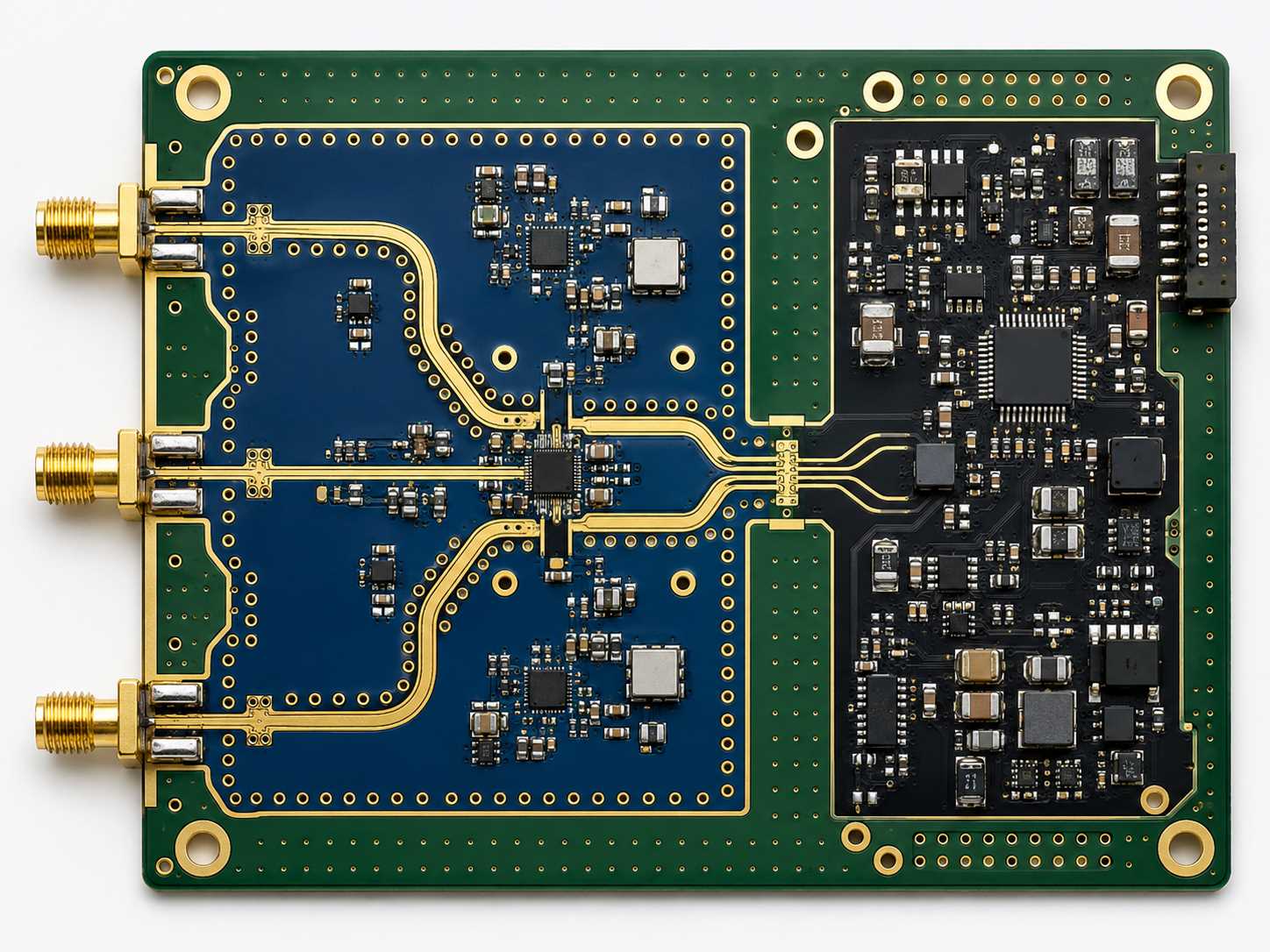
RF Microwave PCB

To discuss an RF microwave PCB project, customers can contact sales@bestpcbs.com with Gerber files, stackup, material requirements, quantity, and assembly needs.

FAQs About RF Microwave PCB

What is the difference between RF PCB and microwave PCB?
RF PCB is a broad term for boards that carry radio frequency signals. Microwave PCB usually refers to boards that work at higher frequencies. In many searches, the term RF microwave PCB covers both types.

What materials are commonly used for RF microwave PCB fabrication?
Common materials include Rogers laminates, PTFE-based laminates, ceramic-filled hydrocarbon materials, low-loss RF substrates, and hybrid RF plus FR4 stackups.

Can RF microwave PCB be used for 24GHz and 5G applications?
Yes. RF microwave PCB boards can be used in 24GHz radar, 5G RF modules, antennas, communication systems, and high-frequency sensing products. Here, 24GHz usually refers to radar applications, while 2.4GHz is more commonly used for WiFi, Bluetooth, Zigbee, and other ISM-band wireless devices.

Where can I get metal-backed RF microwave PCB boards?
You can get metal-backed RF microwave PCB boards from manufacturers with both RF material experience and thermal management capability.

EBest Circuit (Best Technology) can provide metal-backed RF microwave PCB boards using aluminum or copper base structures to support heat dissipation in high-power RF and microwave applications. For projects that need low-loss materials, controlled impedance, and stable thermal performance, EBest can also support DFM review, material selection, PCB fabrication, assembly, and testing.

Does RF microwave PCB require controlled impedance?
In most cases, yes. Controlled impedance helps reduce reflection and signal loss. Many RF traces use 50 ohm impedance, but the final value depends on the circuit design.

Can EBest support RF microwave PCB assembly?
Yes. EBest supports RF microwave PCB fabrication, component sourcing, SMT assembly, testing, and turnkey electronics manufacturing.

How do I request RF microwave PCB production quotes?
Prepare Gerber files, stackup, material type, copper thickness, board thickness, surface finish, impedance target, quantity, and assembly needs. Clear data helps the manufacturer quote faster and more accurately.

If you are not sure whether your RF microwave PCB design is ready for production, EBest Circuit (Best Technology) can review your files and provide practical manufacturing feedback. You can send your Gerber files and project requirements to sales@bestpcbs.com for a technical review and quotation.
You may also like

Best RF Microwave PCB Fabrication for Industrial Applications: A Complete Engineer’s Guide
Wednesday, February 11th, 2026

If you’re an engineer working on industrial systems—from medical imaging to aerospace telemetry—you know that best RF microwave PCB fabrication for industrial applications isn’t just a “nice-to-have”; it’s the backbone of reliable, high-performance equipment. The wrong fabrication choices lead to signal loss, frequency drift, and costly system failures—problems no industrial project can afford. This guide breaks down everything you need to know about best RF microwave PCB fabrication for industrial applications, from material selection to process control, real-world case studies, and how to avoid common pitfalls that plague even experienced teams.

Best RF Microwave PCB Fabrication for Industrial Applications

What Makes the Best RF Microwave PCB Fabrication for Industrial Applications Stand Out?

The best RF microwave PCB fabrication for industrial applications differs from standard PCB manufacturing in three non-negotiable ways: strict impedance control, low-loss material consistency, and precision manufacturing tolerances—all tailored to the harsh conditions of industrial use (extreme temperatures, vibration, humidity). Industrial RF microwave PCBs operate at frequencies above 1GHz (often up to 77GHz for radar systems), where even a 0.1mm etching deviation or 0.05 dielectric constant (Dk) fluctuation can render a board useless.

Key Differentiators of Industrial-Grade RF Microwave PCB Fabrication

  • Impedance Tolerance ±5% or Tighter: Critical for signal integrity; industrial systems (like aerospace telemetry) require consistent impedance to avoid reflection and signal distortion.
  • Low Dissipation Factor (Df ≤ 0.001): Minimizes signal loss, which is essential for long-range industrial communication and high-power applications.
  • High-Temperature Stability: PCBs must maintain performance from -40°C to 125°C (or higher for aerospace), resisting warpage and material degradation.
  • Precision Etching (±0.04mm): Ensures accurate trace widths for RF paths, especially for microstrip and stripline designs common in industrial sensors.

Which Materials Are Best for RF Microwave PCB Fabrication in Industrial Applications?

Best RF Microwave PCB

Material selection is the single most important factor in best RF microwave PCB fabrication for industrial applications—your choice directly impacts signal loss, temperature stability, and overall reliability. For industrial use, two material categories dominate: PTFE-based laminates (for high performance) and hybrid stackups (for balanced performance and mechanical stability).

Top Materials for Industrial RF Microwave PCBs

Material TypeKey PropertiesBest Industrial ApplicationsExample Brands
PTFE-Based (Rogers RO4350B)Dk=3.48, Df=0.0037, low water absorption, high temperature stabilityAerospace radar, medical imaging, high-power industrial sensorsRogers, Taconic, Arlon
PTFE/FR-4 HybridPTFE for RF layers, FR-4 for control/power layers; balances performance and stiffnessIndustrial IoT, 5G backhaul, low-power radarRogers + FR-4, Isola Hybrid
Modified FR-4 (Megtron 6)Dk=3.6, Df=0.004, excellent mechanical strength, stable performance at mid-frequenciesIndustrial control systems, low-frequency RF sensorsPanasonic, Isola

How to Control Impedance in Best RF Microwave PCB Fabrication for Industrial Applications?

Impedance control is non-negotiable for best RF microwave PCB fabrication for industrial applications—without it, signal reflection, attenuation, and crosstalk will destroy performance. Industrial RF microwave PCBs typically require 50Ω (for most sensors/radar) or 75Ω (for communication systems) impedance, with a tolerance of ±5% (±3% for aerospace/medical).

Step-by-Step Impedance Control Process

  1. Design Optimization: Use impedance calculation tools to define trace width, dielectric thickness, and copper weight. For microstrip lines, the formula Z₀ = 87/√(dk + 1.41) × ln(5.98h/(0.8w + t)) ensures accurate impedance (h=dielectric thickness, w=trace width, t=copper thickness).
  2. Material Consistency: Source materials with tight Dk tolerance (±0.05) and test every batch with a Keysight N1500A dielectric tester to avoid fluctuations.
  3. Precision Etching: Use electroformed stencils (±0.005mm accuracy) and control etching parameters (temperature 45±2°C, spray pressure 2.5±0.2kg/cm²) to maintain trace width consistency.
  4. Post-Fabrication Testing: Use Time Domain Reflectometry (TDR) to measure impedance across the board; reject any PCBs with deviations beyond ±5%.

What Are the Common Fabrication Challenges for Industrial RF Microwave PCBs?

Industrial RF microwave PCB fabrication faces unique challenges due to strict performance requirements and harsh operating environments. The most common issues are signal loss, warpage, and dielectric inconsistency—but all are avoidable with proper process control.

Top Challenges and Engineering Solutions

  • Signal Loss from Poor Surface Finish: Solution: Use immersion gold (0.1μm minimum thickness) instead of HASL—gold has lower resistivity (2.4μΩ·cm) and minimizes insertion loss at high frequencies.
  • Warpage in Hybrid Stackups: Solution: Maintain symmetrical stackups (equal copper weight on both sides) and control lamination parameters (175±5°C, 35±2kg/cm² pressure) to avoid resin unevenness.
  • Dielectric Degradation from Moisture: Solution: Store materials in dry environments (RH≤40%) and pre-bake PCBs at 120°C for 40 minutes before fabrication to remove moisture.
  • Crosstalk Between RF Traces: Solution: Separate RF traces by at least 3x the trace width and use ground planes between signal layers to block interference.

How Does Thermal Management Impact Industrial RF Microwave PCB Fabrication?

Thermal management is critical for best RF microwave PCB fabrication for industrial applications—high-power industrial systems (like microwave heaters or radar transmitters) generate significant heat, which degrades dielectric performance and causes component failure. Effective thermal design ensures PCBs maintain stability at operating temperatures up to 150°C.

Proven Thermal Management Techniques

  • Thick Copper Layers: Use 2–6oz copper for power and ground planes to improve heat dissipation—thicker copper has lower resistance and spreads heat faster.
  • Thermal Vias: Place high-density thermal via arrays (0.2mm diameter, 0.5mm pitch) under heat-generating components to transfer heat to the backplane.
  • Metal Backplanes: For extreme heat applications (aerospace), bond a copper or aluminum backplane to the PCB to enhance thermal conductivity.
  • Low-Thermal-Expansion Materials: Use Rogers RO3003 (CTE=6.4ppm/°C) to match the CTE of semiconductor components, reducing thermal stress and solder joint failure.

What Are the Quality Control Standards for Best RF Microwave PCB Fabrication for Industrial Applications?

Industrial RF microwave PCBs require rigorous quality control (QC) to meet performance and reliability standards—especially for medical and aerospace applications, where failure is catastrophic. QC must span material incoming inspection to final testing, with documented processes to ensure consistency.

Critical QC Checks for Industrial RF Microwave PCBs

  1. Incoming Material Inspection: Test Dk, Df, and copper thickness for every material batch; reject batches with Dk fluctuation >±0.05 or copper weight deviation >±10%.
  2. Process Control Checks: Monitor lamination temperature, etching rate, and stencil alignment every 2 hours; log all parameters for traceability.
  3. Electrical Testing: Perform TDR (impedance), insertion loss (IL), and return loss (RL) testing—industrial PCBs require IL ≤0.1dB/inch at 10GHz and RL ≤-15dB.
  4. Environmental Testing: Conduct thermal cycling (-40°C to 125°C, 1000 cycles) and humidity testing (85°C/85% RH, 1000 hours) to ensure long-term reliability.
  5. Visual Inspection: Use 20x microscopes to check for etching defects, solder bridges, and surface finish uniformity; reject boards with any visible flaws.

What Industrial Applications Rely Most on High-Quality RF Microwave PCB Fabrication?

Numerous industrial sectors depend on best RF microwave PCB fabrication for industrial applications, as their systems require high-frequency signal integrity, reliability, and durability. Below are key industries, with real-world case studies showing how proper fabrication solves critical challenges.

Key Industries + Real-World Case Studies

1. Aerospace & Defense

Aerospace radar systems (24GHz/77GHz) require PCBs with ultra-low loss and temperature stability. A major aerospace contractor approached us for PCB fabrication for a satellite telemetry system—their previous supplier’s boards suffered from frequency drift (-0.5GHz) at extreme temperatures. We used Rogers RO4003C (Df=0.001) with a hybrid stackup, precision etching (±0.03mm), and thermal via arrays. The final PCBs maintained impedance ±3% and frequency stability from -55°C to 150°C, passing all aerospace qualification tests.

2. Medical Devices

Medical imaging systems (e.g., MRI RF coils) need PCBs with low signal loss and biocompatibility. A medical device manufacturer needed PCBs for a portable ultrasound machine—their existing boards had insertion loss >0.3dB/inch, degrading image quality. We used immersion gold surface finish, PTFE-based laminates, and optimized trace design to reduce IL to ≤0.08dB/inch. The PCBs met ISO 13485 standards and improved image clarity by 30%.

3. Industrial Equipment

Industrial IoT sensors (5G-enabled) require PCBs that resist vibration and humidity. A factory automation client needed PCBs for a wireless temperature sensor—their previous boards failed due to moisture-induced dielectric degradation. We used moisture-resistant PTFE laminates, vacuum-sealed fabrication, and conformal coating. The PCBs operated reliably in 95% RH environments for 2+ years without performance loss.

How to Choose a Manufacturer for Best RF Microwave PCB Fabrication for Industrial Applications?

Choosing the right manufacturer is as critical as design and material selection for best RF microwave PCB fabrication for industrial applications. Industrial-grade fabrication requires specialized equipment, engineering expertise, and a proven track record in serving medical, aerospace, and industrial sectors.

Key Criteria for Selecting a Manufacturer

  • Specialized Capabilities: Ensure they offer PTFE/hybrid stackups, impedance control ±3–5%, and precision etching (±0.04mm or tighter).
  • Industry Certifications: Look for ISO 9001, ISO 13485 (medical), and AS9100 (aerospace) to ensure compliance with industrial standards.
  • Testing Capabilities: They must have TDR, network analyzers, and environmental testing equipment to verify performance.
  • Case Study Experience: Ask for references in your industry—experience with similar applications reduces risk of failure.
  • Engineering Support: Choose a manufacturer that offers DFM (Design for Manufacturability) support to optimize your design for fabrication.

What’s the Difference Between Industrial and Commercial RF Microwave PCB Fabrication?

Many engineers confuse industrial and commercial RF microwave PCB fabrication—but the two differ drastically in performance requirements, materials, and QC standards. Commercial PCBs prioritize general usability; industrial PCBs prioritize reliability and durability in harsh conditions.

CriteriaIndustrial RF Microwave PCB FabricationCommercial RF Microwave PCB Fabrication
Impedance Tolerance±3–5%±10%
Material QualityPTFE/hybrid laminates (Df ≤0.0037)Standard FR-4 (Df ≥0.01)
Temperature Range-40°C to 150°C (or higher)0°C to 70°C
QC Standards100% electrical/environmental testingSampling testing only
Reliability FocusLong-term (10+ years) performanceShort-term (2–5 years) use

How to Optimize RF Microwave PCB Design for Industrial Fabrication?

Design optimization is key to achieving best RF microwave PCB fabrication for industrial applications—even the best manufacturer can’t fix a poorly designed board. The goal is to minimize signal loss, crosstalk, and thermal stress while ensuring manufacturability.

Essential Design Tips for Industrial RF Microwave PCBs

  • Minimize Trace Length: Keep RF traces as short and straight as possible to reduce insertion loss and phase shift.
  • Use Ground Planes Effectively: Add a solid ground plane under all RF traces to reduce crosstalk and improve impedance consistency.
  • Avoid Right-Angle Bends: Use 45° bends or curves for RF traces—right-angle bends cause signal reflection and impedance mismatch.
  • Separate RF and Digital Layers: Place RF traces on dedicated layers, separated from digital/analog layers by ground planes to block interference.
  • Optimize Component Placement: Place RF connectors and components close to the edge of the board to minimize trace length; keep heat-generating components away from sensitive RF paths.

What Are the Latest Trends in Best RF Microwave PCB Fabrication for Industrial Applications?

The industrial RF microwave PCB fabrication industry is evolving to meet the demands of 5G, IoT, and advanced aerospace/medical systems. The latest trends focus on higher frequency support, miniaturization, and more sustainable manufacturing—all while maintaining industrial-grade reliability.

Top 2026 Trends for Industrial RF Microwave PCBs

  • Millimeter-Wave Fabrication: As industrial radar and 5G systems move to 60–77GHz, manufacturers are adopting advanced techniques (like laser drilling and thin-film deposition) to support these frequencies.
  • Miniaturization: Industrial IoT sensors require smaller PCBs—trends include finer line widths (0.05mm), smaller vias (0.1mm), and integrated passives to reduce board size.
  • Sustainable Materials: Eco-friendly PTFE alternatives (like recycled high-frequency laminates) are gaining traction, meeting industrial performance requirements while reducing environmental impact.
  • Automated Fabrication: AI-driven process control (for etching, lamination, and testing) improves consistency and reduces human error—critical for industrial QC.

FAQ: Common Questions About Best RF Microwave PCB Fabrication for Industrial Applications

Q1: Do industrial RF microwave PCBs always need PTFE-based materials?

No—PTFE is ideal for high-frequency (above 5GHz) or high-reliability applications (aerospace/medical), but modified FR-4 (like Megtron 6) works for lower-frequency industrial systems (1–5GHz). The key is matching the material’s Dk/Df to your operating frequency.

Q2: What impedance tolerance do I need for industrial RF microwave PCBs?

Most industrial applications require ±5% impedance tolerance. For critical applications (aerospace radar, medical imaging), use ±3% to ensure signal integrity. Anything wider than ±10% will cause significant reflection and signal loss.

Q3: How can I reduce signal loss in industrial RF microwave PCB fabrication?

Reduce signal loss by using low-Df materials (Df ≤0.0037), immersion gold surface finish, short/straight RF traces, and impedance control. Avoid HASL (high solder mask loss) and ensure proper ground plane design to minimize crosstalk.

Q4: What environmental tests are required for industrial RF microwave PCBs?

Industrial PCBs typically require thermal cycling (-40°C to 125°C, 1000 cycles), humidity testing (85°C/85% RH, 1000 hours), and vibration testing (10–2000Hz) to ensure durability. Medical/aerospace may require additional tests (e.g., radiation hardness for satellites).

Q5: Can hybrid stackups (PTFE + FR-4) be used for high-power industrial applications?

Yes—hybrid stackups are ideal for high-power industrial applications. Use PTFE for RF layers (low loss) and FR-4 for control/power layers (mechanical stiffness). Ensure symmetrical stackups and proper lamination to avoid warpage.

Q6: How long does industrial RF microwave PCB fabrication take?

Lead times vary by complexity: simple 2-layer boards take 5–7 days, while complex 8-layer hybrid boards (with impedance control and testing) take 10–14 days. For aerospace/medical, add 3–5 days for additional QC and certification.

Q7: What’s the most common mistake in industrial RF microwave PCB fabrication?

The most common mistake is neglecting material consistency—using low-quality laminates with wide Dk fluctuations leads to frequency drift and signal loss. Always source materials from reputable suppliers and test every batch before fabrication.

Why Choose EBest for Best RF Microwave PCB Fabrication for Industrial Applications?

At EBest, we specialize in best RF microwave PCB fabrication for industrial applications, with decades of experience serving aerospace, medical, and industrial equipment manufacturers. Our capabilities include PTFE/hybrid stackups, impedance control ±3–5%, precision etching, and rigorous QC testing to meet ISO 9001, ISO 13485, and AS9100 standards. We offer DFM support to optimize your design, real-world case study expertise, and reliable lead times to keep your projects on track. Whether you need prototype or high-volume production, we deliver industrial-grade RF microwave PCBs that perform in the harshest conditions. We provide best RF microwave PCB fabrication for industrial applications—if you need high-quality, reliable RF microwave PCBs for your industrial project, contact us today to place your order at sales@bestpcbs.com.

You may also like

Top 10 RF Microwave PCB Manufacturers for High-Power Applications
Thursday, December 4th, 2025

High-power RF and microwave systems—such as RF amplifiers, 5G base stations, radar modules, satellite communication units, and microwave transmitters—require PCBs that can maintain stable performance under intense thermal and electrical stress. Ordinary FR-4 boards simply cannot handle the dielectric loss, heat generation, tight impedance requirements, and frequency-dependent behavior seen above 1 GHz.

In this guide, we highlight the Top 10 RF microwave PCB manufacturers for high-power applications—ideal for RF amplifiers, radar systems, 5G infrastructure, satellite communication, and other high-frequency uses.

Top 10 RF Microwave PCB Manufacturers for High-Power Applications

Why You Need a Specialized RF Microwave PCB Manufacturer?

High-power RF designs introduce challenges such as elevated heat, strict impedance requirements, and performance losses at microwave frequencies. Manufacturers must have:

  • Expertise in low-loss materials like Rogers, Taconic, or PTFE-based substrates
  • Multi-layer RF/microwave stackup engineering
  • High-precision etching and drilling for mmWave designs
  • Support for heat-sink integration, metal-backed PCBs, or thick-copper construction
  • Robust quality systems for aerospace/defense-grade reliability

Choosing the right vendor ensures stable power handling, lower insertion loss, and consistent performance across your operating frequency range.

Top 10 RF Microwave PCB Manufacturers for High-Power Applications

1. American Standard Circuits (ASC)

ASC is one of the most experienced RF microwave PCB manufacturers in North America. They specialize in complex high-power designs, including:

  • Metal-backed PCBs for heat dissipation
  • PTFE-based microwave laminates (Rogers, Taconic, Isola)
  • Tight impedance control
  • High-layer-count microwave PCBs

Best for: High-power RF, metal-backed microwave PCBs, aerospace/defense

Their engineering support for thermal-management and high-frequency performance makes them ideal for RF amplifiers and transmitters.

Top 10 RF Microwave PCB Manufacturers for High-Power Applications

2. HT Global Circuits

HT Global produces RF microwave PCBs operating up to 77 GHz and beyond. Their strengths include:

  • Multi-layer PTFE stackups
  • 2–20 layer RF/microwave builds
  • Heavy copper up to 6 oz for high-power devices
  • Hybrid stackups combining FR-4 with RF materials

They are a top choice for automotive radar, mmWave modules, and high-power RF designs.

Best for: mmWave, radar, low-loss PTFE boards, thick-copper RF PCBs

3. Summit Interconnect

Summit Interconnect is known for premium high-frequency and high-reliability microwave PCBs used in:

  • Aerospace
  • Defense
  • Telecom infrastructure

Their fabrication process emphasizes precision drilling, micro-vias, and controlled dielectric thickness—critical for high-frequency energy transfer and low insertion loss.

Best for: Mission-critical high-frequency systems

4. KKPCB

KKPCB works extensively with RF laminates such as Rogers, Isola, Taconic, and Panasonic materials. Their capabilities include:

  • Rigid, flex, and rigid-flex RF PCBs
  • Controlled impedance routing
  • Low-loss dielectric materials
  • High-density microwave layouts

A good mid-cost option for commercial RF/microwave products and 5G devices.

Best for: Telecom, 5G, RF modules

5. Highleap Electronics

Highleap supports complex microwave PCB builds requiring:

  • Hybrid materials
  • Multi-layer RF stackups
  • Cavity/RF shielding structures
  • Precise copper-weight control

Ideal for radar, satellite systems, and advanced RF sensing.

Best for: Multi-layer high-frequency and mmWave PCBs

6. RayMing Technology (RayPCB)

RayMing is widely referenced as a top microwave PCB manufacturer. Their key strengths include:

  • PTFE + hybrid dielectric combinations
  • High-frequency up to mmWave
  • ENIG, ENEPIG finishes for RF connectors
  • HDI for mixed digital + RF sections

Great for high-frequency testing equipment, RF sensors, and wireless communication modules.

Best for: Broad RF material selection, advanced stackups

7. WellPCB

WellPCB provides high-frequency PCBs up to 64 layers with:

  • Tight impedance tolerances
  • Low-loss laminates (Rogers, Isola, Taconic)
  • Quick-turn RF prototyping capability

A strong choice for R&D labs, engineering teams, and rapid iteration cycles.

Best for: Low-loss microwave PCBs and prototype runs

8. Sanmina Corporation

Sanmina serves enterprise and industrial markets requiring:

  • High-reliability RF PCB mass production
  • Telecom and infrastructure RF boards
  • Integrated assembly + testing

If your product needs scale, Sanmina is a top-tier partner.

Best for: High-volume microwave PCB production

9. TTM Technologies

TTM is one of the world’s largest PCB manufacturers with deep expertise in:

  • Microwave PCBs for defense/avionics
  • Very tight tolerance stackups
  • Hybrid laminates for both RF + digital

Perfect for mission-critical high-power RF systems.

Best for: High-reliability aerospace/defense RF PCBs

10. EBest Circuit (Best Technology) (BEST TECH)

EBest Circuit (Best Technology) stands out for its deep expertise in Rogers, Taconic, PTFE, ceramic-filled laminates, and hybrid RF stackups. Our core strengths include:

  • High-power RF PCB manufacturing with thick copper
  • PTFE microwave PCBs for >10 GHz
  • Cavity structures, tight impedance control, and controlled Dk/Df
  • RF prototype-to-production support

We are especially strong in thermal management, cost-effective PTFE processing, and mixed-material high-frequency boards used in RF amplifiers and microwave modules.

Best for: Custom high-power RF PCB manufacturing & PTFE-based microwave PCBs

What Should You Provide for High-Power RF PCBs?

When ordering high-power RF microwave PCBs, your manufacturer needs precise engineering data to ensure correct impedance, dielectric performance, and thermal stability. Below is a complete checklist.

1. Operating Frequency Range

Specify the exact frequency band, such as:

  • 1–6 GHz (RF)
  • 10–30 GHz (Microwave)
  • 24–77 GHz (mmWave)

Higher frequencies require lower-loss materials and tighter tolerances.

2. Target Impedance & Tolerance

Provide the intended impedance values such as:

  • 50Ω microstrip
  • 75Ω signal lines
  • Differential RF pairs

This allows the PCB manufacturer to determine trace width, spacing, copper thickness, and dielectric thickness.

3. Expected Power Handling / Heat Load

Thermal load affects stackup and material choice, especially for:

  • RF amplifiers
  • High-power transmitters
  • Power combiners/splitters

Manufacturers may include metal-backed substrates or copper coins if required.

4. Material Preferences

List materials if known:

  • Rogers 4350B, 4003C, 5880, 3006
  • Taconic TLX, TLY, RF-35
  • Isola Astra / I-Tera HT / PTFE laminates

Or request material recommendations based on your frequency and power.

5. Stackup Requirements

Specify:

  • Number of layers
  • Hybrid stackup (PTFE + FR-4)
  • Dielectric thickness
  • Copper weight (e.g., 1oz, 2oz, 3oz+)

High-power RF typically needs high-copper layers for heat dissipation.

6. RF-sensitive Structure Information

Provide details on:

  • RF cavities
  • Via fences / Ground vias
  • Via-in-pad for RF chips
  • Microstrip or stripline routing

These influence manufacturability and RF performance.

7. Connector Type & Finish

RF connectors need stable surface performance:

  • ENIG
  • ENEPIG
  • Hard gold

Let the manufacturer know if you’re using SMA, MMCX, SMP, or edge-launch connectors. Please remember, the more detailed information you provided, the fast you get your prototype.

What Should You Provide for High-Power RF PCBs?

What Should You Provide for High-Power RF PCBs?

Why EBest Circuit (Best Technology) Is Your Best Partner?

EBest Circuit (Best Technology) is one of the most leading radio frequency manufacturers in Asia, we have more than 19 years experienced in this field. Our team deeply specializing in high-power RF PCBs and PTFE-based microwave PCB fabrication. Here’s why we stand out for most years:

1. Expertise in High-Frequency Materials

BEST TECH processes complex RF materials including:

  • Rogers (4350B, 5880, 3003)
  • Taconic
  • Teflon/PTFE
  • Ceramic-filled laminates

2. Superior High-Power Handling Capability

Their thick-copper RF PCB options (2–6 oz) ensure stable thermal performance in:

  • Power amplifiers (PA)
  • High-power transmitters
  • RF power distribution networks

3. Precision Fabrication & Tight Impedance Control

With advanced drilling, lamination, and copper etching technologies, they achieve:

  • ±5% impedance tolerance
  • Excellent line width stability
  • Accurate dielectric thickness across the panel

4. RF Prototyping + Mass Production

From engineering samples to volume production, EBest Circuit (Best Technology) supports fast lead times with stable process control.

5. Competitive Pricing for PTFE & Microwave Boards

Compared with Western manufacturers, BEST TECH offers better pricing while maintaining high quality—ideal for startups, R&D teams, and cost-sensitive RF applications.

If you are interested in RF PCB design or want to get your first RF PCB prototype with fast delivery, please do not hesitate to contact us, our sales team are engineered sales, they deeply know the RF PCB, and enable to provide you the best solution and competitive price in short time.

FAQs

1. What is an RF microwave PCB?

An RF microwave PCB is a printed circuit board designed to operate at high frequencies (1–100+ GHz). It uses low-loss materials such as Rogers or PTFE to maintain stable impedance and minimize signal attenuation.

2. What causes high-power RF PCBs to fail?

Common failure causes include:

  • Excessive heat
  • Poor thermal design
  • Incorrect stackup selection
  • Impedance mismatch
  • Delamination from improper lamination of PTFE materials

Choosing the right RF PCB manufacturer greatly reduces failure risk.

3. What is the recommended copper thickness for high-power microwave PCBs?

For heat-heavy RF circuits:

  • 2 oz or 3 oz copper is common
  • 4–6 oz for very high-power amplifiers

4. Why is controlled impedance so important in RF PCB design?

Proper impedance ensures:

  • Lower insertion loss
  • Minimal signal reflection
  • Stable RF phase and amplitude
  • Accurate high-frequency performance

5. Can I use FR-4 for microwave PCBs?

FR-4 is not recommended above 3–6 GHz due to high dielectric loss. For microwave frequencies, PTFE or Rogers materials are necessary.

You may also like

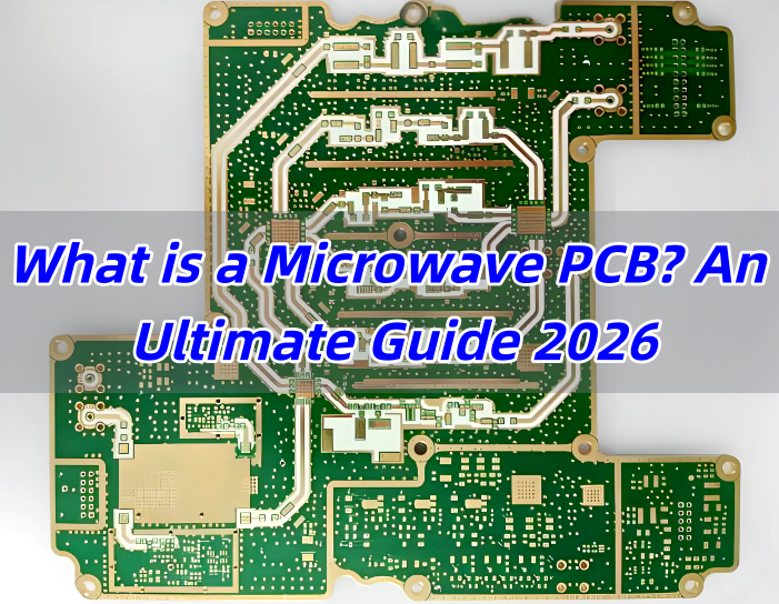
What is a Microwave PCB? An Ultimate Guide 2026
Wednesday, December 3rd, 2025

A microwave PCB handles signals that run at very high frequencies, and these boards support systems that need clean, stable performance. You will find a microwave PCB in equipment such as radar modules, satellite links, high-speed wireless platforms, and precision test devices. As industries push toward higher data rates and smaller RF systems, the need for dependable microwave boards grows quickly.

Today, many engineers search for rf microwave PCB options that keep loss low and impedance steady. Others look for complete rf & microwave PCB solutions that simplify material choice, stack-up planning, and manufacturing. If you’re evaluating RF microwave PCB materials or sourcing RF & microwave PCB solutions, this article will give you a complete understanding.

What is a Microwave PCB? An Ultimate Guide 2026

What Is a Microwave PCB?

A microwave PCB is a printed circuit board designed to operate at extremely high frequencies, typically:

  • Microwave band: 300 MHz – 30 GHz
  • Millimeter-wave (mmWave): 30 – 100+ GHz

At these frequencies, PCB traces behave like transmission lines, and even tiny layout variations can impact signal loss, phase accuracy, antenna performance, and overall system reliability.

Microwave PCBs are commonly used in radar systems, satellite communication, aerospace navigation, and 5G mmWave modules. Compared with standard RF boards, microwave PCBs demand more precise materials, controlled impedance, and stricter fabrication tolerances.

What Materials Are Used for Microwave PCBs?

Material choice is one of the most important decisions in microwave design. Standard FR-4 cannot support microwave frequencies due to high loss and unstable dielectric properties. Instead, microwave PCBs use advanced materials engineered for low loss and tight dielectric tolerances.

Here are the materials most commonly used:

Material TypeExamplesFeaturesBest Use Case
PTFE (Teflon)RT/duroid 5880, Taconic TLYExtremely low loss, stable Dk, best for high GHzRadar, mmWave, satellites
Hydrocarbon CeramicsRogers RO4350B, RO4003CLow loss, easy to manufacture, cost-effective1–20 GHz microwave circuits
Ceramic-Filled PTFERogers RO3006/3010Ultra-stable Dk, low thermal expansionHigh-power microwave and phased arrays
Hybrid StackupsFR4 + RogersPerformance + lower costMixed-signal RF/microwave designs

The best material depends on target frequency, environmental exposure, and mechanical requirements. Each laminate affects loss, phase stability, and long-term reliability.

Key Design Rules and Layout for Microwave PCB Design

Designing a microwave PCB is very different from routing a standard digital or low-frequency board. At microwave frequencies, each copper trace behaves like a transmission line. Small changes in width, dielectric height, copper roughness, or via structure can shift impedance and alter the entire RF chain. Because of that, layout and stack-up design must follow strict engineering rules to keep signal quality stable.

Key Design Rules and Layout for Microwave PCB Design

Below are the core principles used by RF engineers when building reliable microwave layouts.

1. Maintain Tight Impedance Control

Stable impedance is the foundation of microwave design. Even small dimensional changes can introduce reflections or distort the waveform.

Key requirements:

  • Define target impedance early (commonly 50Ω or 75Ω).
  • Choose the correct structure: microstrip, stripline, or grounded coplanar waveguide (GCPW).
  • Keep trace width consistent along the entire path.
  • Maintain stable dielectric thickness and copper thickness.
  • Use field-solver tools (ADS, HFSS, CST, Polar SI, or Altium impedance calculator).
  • Keep differential pairs phase-matched if used in RF mixers or high-frequency paths.

GCPW is widely used for microwave PCB design because it offers strong field confinement and supports compact layouts.

2. Use Smooth Routing Instead of Sharp Corners

High-frequency energy does not like sudden changes. Sharp corners cause impedance shifts and increase local reflections.

Preferred routing practices:

  • Avoid 90° turns.
  • Use gradual curves (arc routing) for cleaner field transitions.
  • Use mitered 45° bends if space is limited.
  • Keep sensitive paths straight and short whenever possible.

Smooth routing helps preserve phase stability and reduces insertion loss.

3. Keep the Ground Plane Continuous

A microwave signal needs a clean, uninterrupted return path. Gaps in the ground plane cause radiation, coupling, and impedance drift.

Ground plane guidelines:

  • Maintain a solid ground layer directly under RF traces.
  • Avoid splits, voids, or cutouts beneath the signal path.
  • Do not place digital return paths through RF areas.
  • Add stitching vias around RF traces to create a “via fence” barrier.

A well-designed ground structure stabilizes the electromagnetic field and reduces unwanted emissions.

4. Manage Vias Carefully

A via is not just a hole at microwave frequencies—it’s a small inductor. Too much via inductance can degrade signal quality.

Best practices for vias:

  • Avoid unnecessary layer jumps.
  • Use multiple parallel vias to lower effective inductance.
  • Keep via barrels short when possible.
  • Add grounding vias around pads and connectors to improve shielding.
  • Avoid routing RF traces directly over via fields or ground voids.

Good via strategy can significantly improve stability in PA, LNA, and filter sections.

5. Select the Right Transmission Line Structure

Different RF paths require different structures depending on frequency, isolation, and mechanical constraints.

Common options:

  • Microstrip – simple, ideal for top-layer routing.
  • Stripline – fully shielded, good for noise-sensitive circuits.
  • Grounded coplanar waveguide (GCPW) – excellent isolation, compact layout, and easy impedance tuning.
  • Wide microstrip – lower conductor loss, suitable for power amplifiers.

GCPW has become the most popular for microwave work due to its predictable behavior and high routing density.

6. Align Components with the Signal Flow

Component orientation affects load matching and return loss.

Component placement guidelines:

  • Place RF blocks (filter, LNA, PA, mixer) in the order of the signal chain.
  • Keep matching networks close to device pins.
  • Avoid unnecessary gaps between RF parts.
  • Place RF connectors, such as SMA or SMP, near the board edge for clean transitions.

When Should You Choose Microwave PCB vs. RF PCB?

Many engineers compare microwave PCBs with standard RF boards because both handle high-frequency signals. But the decision depends on frequency, performance targets, and loss tolerance.

TechnologyFrequency RangeBest For
RF PCBUp to ~6 GHzBluetooth, Wi-Fi, sub-6 GHz communication
Microwave PCB6–100+ GHz5G mmWave, radar, satellite, high-precision sensing

Choose an RF PCB when:

  • Frequencies are below 6 GHz
  • Cost is a major concern
  • FR-4 or mixed-material stackups are acceptable

Choose a Microwave PCB when:

  • You operate above 6 GHz
  • You require ultra-low loss
  • Your system needs stable phase and predictable impedance
  • Applications involve radar, mmWave, or satellite links

In short, microwave PCBs suit high-precision projects where even small layout or material changes can affect real performance. They are the preferred choice for radar, satellite links, and advanced communications.

Microwave PCBs Applications & Industries

Microwave PCBs appear in many sectors because they support stable, low-loss transmission for sensitive circuits. You’ll often see them in systems that require fast data, long-range signal paths, or precise sensing.

Common applications include:

  • 5G and 6G wireless infrastructure
  • Satellite communication systems (SATCOM)
  • Automotive radar (24 GHz, 77 GHz)
  • Military and commercial radar platforms
  • Microwave filters, couplers, and antennas
  • High-frequency power amplifiers
  • Navigation and guidance systems
  • Medical imaging devices such as MRI coils
  • Instrumentation and RF test equipment
  • Industrial microwave heating and sensing

These industries rely on microwave boards because small performance shifts can affect overall system behavior. Stable materials and predictable routing keep these systems accurate and responsive.

Microwave PCBs Applications & Industries

Does Size of a Microwave PCB Affect Its Application?

Yes, board size can influence performance because microwave signals respond to physical dimensions. At these frequencies, even a few millimeters can change how energy travels.

Board size affects:

  • Impedance stability:Longer traces add more loss and potential phase distortion.
  • Resonance behavior:Larger boards can introduce unwanted resonances.
  • Shielding structure:Compact layouts may need tighter via fences.
  • Thermal changes:Bigger boards may expand more under heat, shifting dielectric spacing.
  • Antenna performance:Antenna length and board shape affect radiation patterns.

Small boards require sharper tolerance control. Large boards demand stronger handling of expansion and material stability. The ideal size depends on whether the circuit is an antenna, filter, amplifier, or sensor.

How to Tell If a Microwave Control Board Is Bad?

Many users ask this because microwave ovens and industrial microwave systems depend on small control boards. Failures are often easy to spot once you know what to check. Common signs of a bad microwave control board include:

  • No power, no response, or blank display
  • Buttons that fail to react
  • Burning smell or visible damage
  • Unusual noises or sparking
  • Microwave stops heating while lights and fan still work
  • Random behavior such as auto-starting or shutting off
  • Relays that click repeatedly without function

If above signs occur, you can perform below visual checks safely:

  • Scorch marks or dark spots
  • Swollen capacitors
  • Cracked solder joints
  • Damaged connectors
  • Loose ribbon cables

These symptoms point to circuitry or relay failure. For home microwaves, technicians often replace the entire board rather than repair individual components.

How Much Does It Cost to Repair a Microwave Circuit Board?

Repair cost depends on equipment type, part availability, and labor requirements.

Typical consumer microwave repair ranges:

  • Basic repair: USD 80–120
  • Control board replacement: USD 120–250
  • High-end or built-in models: USD 180–350

Industrial microwave equipment repair ranges:

  • Board-level component repair: USD 250–600
  • Full board replacement: USD 400–1,200+ depending on complexity

Factors that influence cost include:

  • Part scarcity
  • Board size and layer count
  • Number of relays, sensors, or high-voltage circuits
  • Whether the board is conformal-coated
  • Testing and calibration requirements

Consumer microwaves are often cheaper to replace than repair, but industrial microwave systems usually justify board-level repair. EBest Circuit (Best Technology) can repair the microwave circuit board for free if your PCB are ordered from our company.

Where to Get RF Microwave PCB Boards with UL/CE Certification?

Many companies need microwave PCBs that meet safety and compliance standards, especially when the final product enters global markets. UL and CE certifications help confirm material reliability and safety. When sourcing certified microwave boards, a good supplier should provide:

  • UL-certified laminates (Rogers, Taconic, Arlon, Panasonic)
  • CE-compliant production and testing
  • Rogers/PTFE/ceramic microwave PCB fabrication
  • Controlled impedance testing reports
  • Hybrid laminations and multi-layer microwave stackups
  • RF & microwave PCB solutions for 1–100 GHz

EBest Circuit (Best Technology) is a strong option for RF and microwave PCB production because the company offers:

  • UL-approved material systems
  • Stable performance with PTFE, Rogers, and ceramic-filled substrates
  • Tight impedance control for microwave designs
  • Complete CE-related documentation support
  • Strong engineering assistance during stack-up and DFM review
  • Consistent production with IPC standards
  • Fast global delivery for prototypes and batches

If you are preparing a new microwave PCB or RF hardware program, welcome to contact us at sales@bestpcbs.com, our team is 24/7 hours online for you!

You may also like

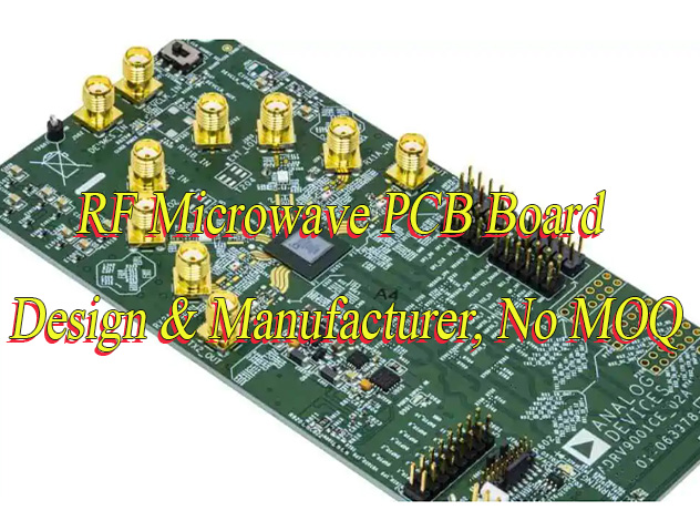
RF Microwave PCB Board Design & Manufacturer, No MOQ
Friday, October 31st, 2025

Why choose RF microwave PCB? Let’s discover definition, benefits, applications, design spec and layout, recommended PCB manufacturer for RF microwave PCBs.

Are you worried about these problems?

  • High-frequency signal loss is high, how to improve RF performance?
  • Above 5GHz, interlayer crosstalk is hard to control, how to ensure signal stability?
  • High-power device thermal design, how to achieve precise temperature control?

As a RF Microwave PCB manufacturer, EBest Circuit (Best Technology) can provide you service and solutions:

  • Substrate customization by frequency band: match low-loss materials with 20% impedance margin to reduce loss.
  • Dual-verified impedance control: error within ±2mil, TDR measured deviation <5%, crosstalk suppressed >20dB.
  • Thermal solution: solder pad + via array + 2oz copper top/bottom layers, thermal resistance <5℃/W, hotspot temperature <85℃.

Welcome to contact us if you have any request for microwave RF PCB: sales@bestpcbs.com.

What Is RF Microwave PCB?

RF Microwave PCB is a specialized circuit board designed for carrying and processing high-frequency signals, typically covering radio frequency (RF) from approximately 300 kHz to 300 GHz and microwave frequencies from 1 GHz to 300 GHz.

Unlike conventional PCBs, it utilizes high-frequency substrate materials such as Rogers, Teflon, or ceramic-filled composites. These materials feature extremely low signal loss, stable dielectric constant, and excellent thermal performance. Its design and manufacturing are highly precise, emphasizing signal integrity through exact control of trace impedance, optimized transmission line structures like microstrip and stripline, minimized parasitic effects, and strict regulation of laminate processes and surface treatments. This ensures efficient, low-distortion, and low-interference transmission of high-frequency or microwave signals on the board.

What Is RF Microwave PCB?

Why Choose RF Microwave PCB?

Benefits of RF Microwave Printed Circuit Board:

  • Stable High-Frequency Signal Transmission: Utilizes low-loss substrates and precise impedance control technology to support GHz-level high-frequency signal transmission. This reduces signal attenuation and crosstalk, ensuring signal integrity in high-speed scenarios such as 5G communications, radar, and satellite equipment, thereby enhancing the reliability of terminal products.
  • Reduced System Energy Consumption and Heat Dissipation Pressure: Optimizes circuit layout and high-performance dielectric materials like PTFE and ceramic-filled composites to achieve low insertion loss and efficient thermal management. This minimizes energy waste, lowers device heat generation, extends product lifespan, and reduces cooling module costs.
  • Compact Design for Miniaturization Needs: Enables high-density multi-layer routing to integrate complex RF modules. This allows precise arrangement of high-frequency components such as filters and amplifiers within limited space, meeting stringent miniaturization and lightweight requirements for smartphones, IoT devices, and other applications, boosting market competitiveness.
  • Superior Anti-Interference and Electromagnetic Compatibility: Incorporates shielding layers, optimized grounding, and electromagnetic simulation validation to effectively suppress high-frequency noise and external interference. This ensures stable device operation in complex electromagnetic environments like industrial control and automotive electronics, reducing failure rates and customer maintenance costs.
  • Accelerated Product Development Cycle: Standardized design processes and mature manufacturing techniques such as laser drilling and electroplating via filling shorten prototype verification and mass production timelines. Combined with Design for Manufacturability (DFM) guidance, this reduces trial production iterations, helping clients seize market opportunities and lower overall development costs.
  • Significant Long-Term Cost Efficiency: Although initial material and process costs are higher, the high reliability, low failure rate, and long-term stability result in reduced repair and replacement frequencies, lowering the total lifecycle cost. This makes it particularly suitable for high-reliability sectors like medical and aerospace applications.
Why Choose RF Microwave PCB?

When to Use RF Microwave PCB Board?

Applications of RF Microwave PCB Board:

  • 5G/6G Communication Base Stations: 5G Massive MIMO Antenna Array (AAU), Base Station RF Front-End Module, Millimeter Wave Small Cell.
  • Satellite Communication Systems: Satellite Onboard Transponder, Ground Station Antenna Feed Network, Low-Earth Orbit Satellite Constellation Terminal.
  • Radar Systems: Automotive 77GHz Millimeter Wave Radar, Military Phased Array Radar, Weather Radar Antenna Feeder.
  • Aerospace Electronics: Airborne Radar System, Satellite Navigation Receiver (GPS/BeiDou), Aircraft Communication Data Link.
  • Microwave Test Instruments: Spectrum Analyzer Signal Processing Module, Network Analyzer Test Port, High-Frequency Signal Generator.
  • Medical Devices: Microwave Ablation Therapy Probe, Medical MRI RF Coil.
  • Wireless Infrastructure: Microwave Backhaul Equipment (Point-to-Point Transmission), Indoor Distribution System Combiner.
  • Automotive Electronics: V2X Vehicular Communication Module (5.9GHz), In-Vehicle Satellite TV Receiver.

RF Microwave PCB Design Technical Parameter

Parameter NameTypical Value/Range
Impedance Control50Ω (Common) / 75Ω (Video)
Dielectric Constant (ε)2.2-10 (FR4: 4.3-4.8)
Loss Tangent (tanδ)0.001-0.025 (High-frequency Boards <0.005)
Substrate Thickness0.2-3.2mm
Copper Foil RoughnessRa<0.5μm (High-frequency Applications)
Glass Fiber EffectWeave Density >7628
Thermal Expansion Coefficient (CTE)X/Y Axis <18ppm/℃, Z Axis <50ppm/℃
Thermal Conductivity0.3-2W/(m·K)
Surface FinishENIG/Immersion Silver/OSP
Line Width Tolerance±10% (Conventional)/±5% (High-frequency)
Layer-to-Layer Alignment Accuracy±25μm (Multilayer Boards)
Dielectric UniformityΔε<5%

RF Microwave PCB Board Design & Layout

1. Substrate Selection and Characteristic Matching

  • Material Expansion Selection: For high-frequency scenarios, recommend Rogers RO4350B, Taconic TLX series; for high-precision scenarios, select Panasonic Megtron 6 (Dk=3.3±0.05, loss<0.002@10GHz) or Isola I-Tera MT40 (Dk=3.45, loss<0.003@5GHz). FR-4 is limited to low-frequency test boards or cost-control scenarios, requiring gold-plating/immersion silver to reduce surface roughness impact.
  • Dynamic Parameter Verification: Use Agilent 85070D Dielectric Constant Tester to measure Dk values, combined with temperature-humidity aging tests to verify long-term stability. Thickness tolerance control requires collaboration with substrate supplier capabilities (e.g., ±5% high-end substrates), and design margin is increased to 25% to address processing errors.
  • Special Scenario Adaptation: Millimeter-wave (>30GHz) applications recommend Liquid Crystal Polymer (LCP) substrate (Dk=3.0, loss<0.0015), paired with microvia arrays for ultra-low loss transmission.

2. Precise Impedance Control and Verification

  • Multidimensional Calculation Verification: Cross-validate using Polar SI9000 and Altium Designer 2D/3D impedance calculators. For non-standard impedances (e.g., 75Ω video signals), optimize line width/dielectric thickness combinations via Taguchi method to ensure process window ≥±3mil.
  • TDR In-Depth Application: Set reference planes near TDR test points, measure single-ended/common-mode impedance via differential probes, and synchronously verify signal integrity metrics (rise time<20ps). For high-speed digital-RF hybrid circuits, use eye diagram instruments to validate timing margins.
  • Differential Pair Optimization: For serpentine differential pairs, validate bending radius impact on impedance via electromagnetic simulation, ensuring length matching error<0.5mil@10GHz.

3. Stack-Up Structure Optimization Design

  • Multilaminate Expansion Scheme: 8-layer boards recommend “Signal-GND-Power-Signal-Power-GND-Signal-Signal” structure with dual GND layers in the middle for dual shielding. 4-layer boards are only suitable for low-power RF modules, requiring blind/buried via technology for interlayer interconnection.
  • Interlayer Coupling Suppression: Insert low-dielectric isolation layers (e.g., Arlon AD300) between adjacent signal layers to reduce interlayer crosstalk>20dB. Power-GND spacing is optimized via finite element analysis to ensure capacitance coupling>90%.
  • Mixed-Signal Processing: For digital-RF hybrid circuits, use “island GND” technology to isolate digital noise, paired with beads/inductors to construct low-pass filter networks.

4. Signal Path Layout Specifications

  • Trace Process Refinement: Use tapered line width technology for smooth impedance transition (e.g., 50Ω to 75Ω) to avoid impedance discontinuity reflections. For microwave signals, adopt coplanar waveguide (CPW) structure with ground via arrays forming a continuous reference plane.
  • Via Optimization Design: Laser microvia technology achieves 0.1mm microvias, paired with back-drilling to eliminate stubs. High-frequency vias require parasitic parameter verification via Ansys Q3D to meet design thresholds.
  • Shielding Structure Upgrade: Set electromagnetic shielding walls around critical signal paths, using nickel/gold plating to enhance shielding effectiveness. For radiation-sensitive devices, use shielding covers + thermal gel composite heat dissipation solutions.

5. Grounding and Shielding Strategies

  • Hybrid Grounding Enhancement: Low-frequency modules use “star grounding” to the main ground terminal; high-frequency modules use “mesh grounding” to reduce ground bounce noise. RF front-end modules adopt “GND-Signal-GND” sandwich structure for dual shielding.
  • Shielding Effectiveness Verification: Use EMxpert near-field scanner to measure shielding effectiveness>60dB@1GHz. Sensitive devices require 3D electromagnetic simulation to validate shielding structure effectiveness.
  • Ground Via Arrays: Adopt “honeycomb” via array layout with spacing≤λ/20@operating frequency to form a continuous Faraday cage. Vias require plating fill technology to enhance reliability.

6. Power Integrity Optimization

  • Decoupling Capacitor Strategy: “0.01μF high-frequency + 10μF low-frequency” capacitor combinations paired with beads to construct multi-stage filter networks. Power noise-sensitive devices use embedded capacitor technology (e.g., buried capacitor layers).
  • PDN Simulation Enhancement: Use Ansys SIwave for full-wave electromagnetic simulation to verify PDN impedance<0.5Ω@3GHz. High-frequency power noise uses power plane segmentation + capacitor bridging technology.
  • Power Plane Optimization: Mesh copper pour enhances current carrying capacity, paired with thermal vias for thermal-electrical co-design. Power planes are validated via voltage drop simulation to ensure drop<3%.

7. Thermal Management and Heat Dissipation Design

  • Heat Dissipation Structure Upgrade: High-power devices use “thermal pad + thermal via + heat sink” three-tier cooling solutions, paired with thermal interface materials to achieve thermal resistance<5℃/W. Millimeter-wave devices use diamond heat sink substrates.
  • Thermal Simulation Verification: Use Ansys Icepak for thermal simulation to validate hotspot temperature<85℃. For high-density layouts, use thermal-electrical-structural co-simulation to ensure thermal stress<material yield strength.
  • Copper Thickness Selection: Top/bottom layers use 3oz copper for enhanced thermal diffusion; inner layers use 1oz copper to balance cost and performance. Extreme environment applications use gold-plating/immersion silver for corrosion resistance.

8. Design for Manufacturability and Testability

  • DFM Check Expansion: Includes line width uniformity, pad size consistency, minimum annular ring verification, etc. Use Valor NPI software for automated checks to meet IPC-6012 standards.
  • Test Point Deepening Design: Use 50Ω SMA interfaces paired with calibration kits for precise testing. High-speed digital signals use differential test points paired with eye diagram instruments for timing validation.
  • File Delivery Expansion: Includes complete Gerber files (impedance layer, pad layer, silkscreen layer, stencil layer) paired with process specification documents (back-drill depth, blind/buried via positions). Use Git version control for document traceability.

9. Simulation Verification and Document Delivery

  • Simulation Tool Expansion: Besides ADS/HFSS, use Keysight ADS Momentum for planar electromagnetic simulation or ANSYS HFSS 3D Layout for full-wave simulation. For time-domain response validation, use SPICE models paired with eye diagram instruments.
  • Document Package Enhancement: Includes design specifications, simulation reports, Gerber files, BOM lists, process specification documents, test reports, etc. Use PDF/A format for long-term readability, paired with digital signatures for tamper-proof validation.
  • Risk Management Strengthening: Use FMEA tools for risk assessment, clarify potential failure modes (crosstalk, hotspots, soldering defects) and solutions. Establish design change tracking systems to ensure all changes are validated and documented.
RF Microwave PCB Board Design & Layout

Why Choose EBest Circuit (Best Technology) as RF Microwave PCB Board Manufacturer?

Reasons why choose us as RF microwave PCB board manufacturer:

  • International Certification Assurance: Holds ISO 9001 quality management system certification and complies with industry-mandated certifications (e.g., medical, automotive, RoHS), ensuring product compatibility with global stringent application scenarios.
  • Free DFM Design Verification: Offers free Design for Manufacturability (DFM) analysis to identify and resolve potential design issues early, reducing development costs and risks while ensuring first-pass manufacturing success.
  • Competitive Pricing: Achieves cost control through optimized production processes and supply chain management, delivering cost-effective RF microwave PCB solutions particularly suitable for budget-sensitive projects.
  • 24-Hour Rapid Prototyping: Supports sample production within 24 hours, enabling quick response to customer needs, shortened R&D cycles, and market opportunity capture, ideal for urgent project validation.
  • Flexible Low-MOQ and Small-Batch Production: Accepts low minimum order quantities (MOQ) and small-batch orders to meet R&D testing, small-scale production, or customization needs, reducing customer inventory pressure and capital tie-up.
  • Strict Full-Process Quality Control: Implements end-to-end quality control from raw material inspection, production monitoring, to final product testing, ensuring each PCB meets high reliability standards and minimizes defect rates.
  • Expert Technical Team Support: Features a team of experienced RF microwave engineers providing full-process technical support from design optimization and material selection to process adjustments to resolve complex technical challenges.
  • Efficient Supply Chain Management: Collaborates deeply with high-quality raw material suppliers to ensure stable material supply and rapid delivery, coupled with optimized production scheduling for on-time and reliable delivery.
  • Customized Service Capability: Offers tailored solutions for special requirements, including high-frequency material selection, impedance control optimization, and specialized surface treatments, to meet diverse project needs.
  • Responsive Customer Service: Provides 24/7 customer support for quick responses to inquiries, order tracking, and after-sales issues, delivering professional advice and solutions to enhance customer experience and trust.
Why Choose EBest Circuit (Best Technology) as RF Microwave PCB Board Manufacturer?

Our RF Microwave PCB Capabilities

ParameterSpecification
Base material:Rogers/Telfon
Board Thickness:0.5mm~3.0mm(0.02″~0.12″)
Copper thickness:0.5 OZ, 1.0 OZ, 2.0 OZ, 3.0 OZ
Outline:Routing, punching, V-Cut
Soldermask:White/Black/Blue/Green/Red Oil
Legend/Silkscreen Color:Black/White
Surface finishing:Immersion Gold, HASL, OSP
Max Panel size:600*500mm(23.62″*19.68″)
Packing:Vacuum/Plastic bag
Samples L/T:7~9 Days
MP L/T:8~10 Days

Our Quality Certification

  • ISO9001:2015: Universal quality management system covering design, production, and service. Enables continuous improvement via internal audits, KPI monitoring, and customer-centric processes.
  • ISO13485:2016: Medical device-specific certification focusing on lifecycle risk management, regulatory compliance, and supply chain traceability. Includes design validation, sterilization verification, and adverse event reporting.
  • RoHS: Environmental standard limiting 10 hazardous substances (e.g., Pb, Hg, Cd) in electrical/electronic equipment. Mandates homogeneous material testing and supplier declarations of conformity.
  • IATF16949: Automotive quality standard emphasizing defect prevention through APQP, PPAP, SPC, and FMEA. Ensures supply chain collaboration and customer-specific requirement compliance.
  • AS9100D: Aerospace quality system for safety-critical components. Mandates configuration management, design change traceability, NDT testing, and first article inspection (FAI) via ERP/MES systems.

How to Get A Quote for Your RF Microwave PCB Project?

Checklist for RF microwave PCB project quotations:

  • Layer and Structure: Specify layer count (e.g., 4/6/8 layers), board thickness (e.g., 1.0mm/1.6mm), and core layer positions.
  • Substrate Parameters: Indicate high-frequency substrate model (e.g., Rogers RO4350B), dielectric constant (Dk), and dissipation factor (Df).
  • Trace Precision: Minimum trace width/spacing (e.g., 50μm/50μm), impedance value (e.g., 50Ω±10%).
  • Surface Finish: Select options like ENIG, OSP, or electroless nickel gold, with thickness specifications (e.g., ENIG: 3-5μm Ni / 0.05-0.2μm Au).
  • Drill Requirements: Minimum mechanical/laser drill diameter (e.g., 0.15mm/0.075mm), hole wall copper thickness (≥25μm).
  • Testing Standards: Include impedance testing (TDR), signal integrity testing (e.g., S-parameters), and reliability testing (e.g., thermal shock).
  • Quantity & Lead Time: Clarify order quantity (e.g., prototype: 5pcs) and phased delivery timelines (e.g., engineering review: 3 days, production: 10 days).
  • Documentation: Provide Gerber files, BOM, assembly drawings, and process specifications.
  • Environmental Compliance: Meet RoHS/REACH standards, offer halogen-free options, and specify flame retardancy rating (e.g., UL94-V0).
  • Special Requirements: Include thermal management (e.g., metal-core boards), EM shielding, embedded components, or rigid-flex structures.

Welcome to contact us if you have any request for RF microwave PCB: sales@bestpcbs.com.

You may also like