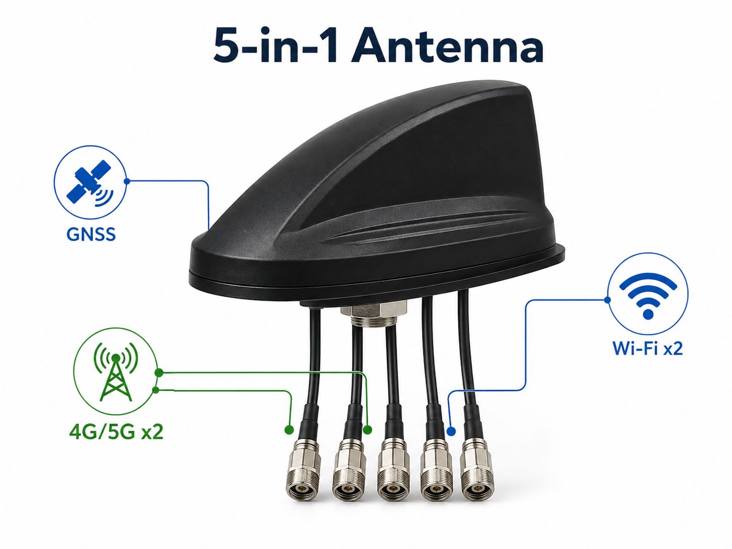
A 5-in-1 antenna usually combines GNSS, 4G/5G cellular, and Wi-Fi signal paths in one antenna unit. It is common in IoT gateways, vehicle trackers, industrial routers, smart transportation devices, and outdoor wireless terminals.
This guide focuses on the checks a PCB/PCBA manufacturer can realistically support before fabrication, assembly, and shipment. In many 5-in-1 antenna PCB and PCBA projects, the antenna is connected through RF interfaces such as SMA connector PCB, SMB PCB, UFL Connector PCB, BNC PCB, or MMCX PCB. If your wireless device requires RF connector assembly, controlled impedance PCB fabrication, or PCBA production review, you can send your Gerber files, BOM, and assembly requirements to sales@bestpcbs.com.
What Is a 5-in-1 Antenna?
A 5-in-1 antenna is an integrated antenna solution with five wireless signal paths. A common structure includes:
- 1x GNSS antenna
- 2x 4G/5G cellular MIMO antennas
- 2x Wi-Fi MIMO antennas
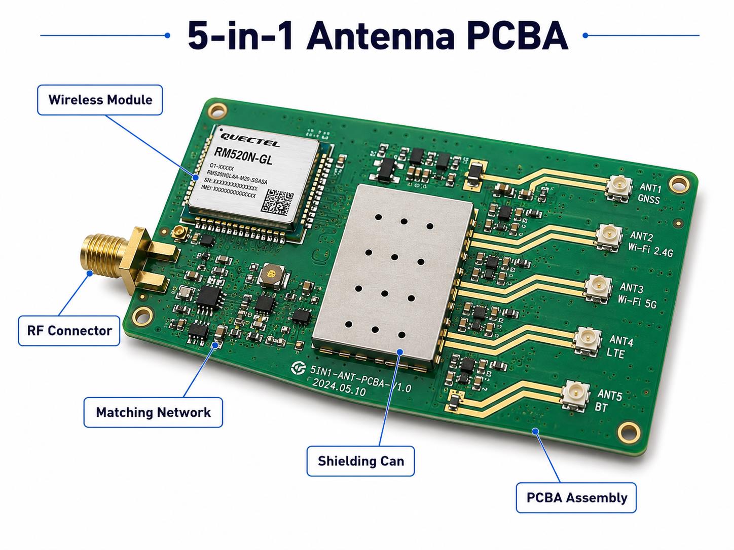
In a real device, the antenna connects to the PCB assembly through RF connectors, coaxial cables, wireless modules, matching circuits, ESD protection parts, and controlled impedance traces.
A PCB/PCBA manufacturer does not replace the antenna engineer. Its value is to check whether the PCB files, stackup, impedance notes, RF connector footprint, BOM, assembly drawing, and test requirements are ready for production.
Common PCB and PCBA Risks in 5-in-1 Antenna Projects
| Problem Found Later | Common Manufacturing Cause | What Should Be Checked Early |
|---|---|---|
| Weak GNSS reception | Poor RF path control or unclear layout notes | GNSS path, impedance note, connector area, module guide |
| Unstable 4G/5G connection | Impedance mismatch or connector issue | 50Ω trace, stackup, RF connector footprint |
| Poor Wi-Fi performance | Trace discontinuity or cable assembly issue | Wi-Fi RF path, connector placement, coaxial cable route |
| Prototype works, batch varies | Stackup changed or impedance not controlled | Stackup drawing, impedance coupon, fabrication tolerance |
| RF connector becomes loose | Wrong footprint or weak pad design | Connector datasheet, pad size, solder mask opening |
| RF matching issue | Wrong value or misplaced small components | BOM, placement file, first article inspection |
| Shielding issue | Poor soldering or incomplete grounding | Shielding can footprint, solderability, ground pads |
These problems are expensive because they often appear after SMT assembly or final testing. Early manufacturing review is much cheaper than redesign, rework, or repeated debugging.
What Should Be Checked Before PCB Fabrication?
Before PCB fabrication, the main task is to confirm whether the board data can support stable RF-related production.
1. Stackup
Stackup affects impedance, trace width, return path, and signal loss. For antenna-related products, stackup should be confirmed before production.
Check:
- Layer count
- Dielectric thickness
- Copper thickness
- RF reference layer
- Solder mask condition
- Material availability
- Impedance tolerance
2. 50Ω RF Trace Requirement
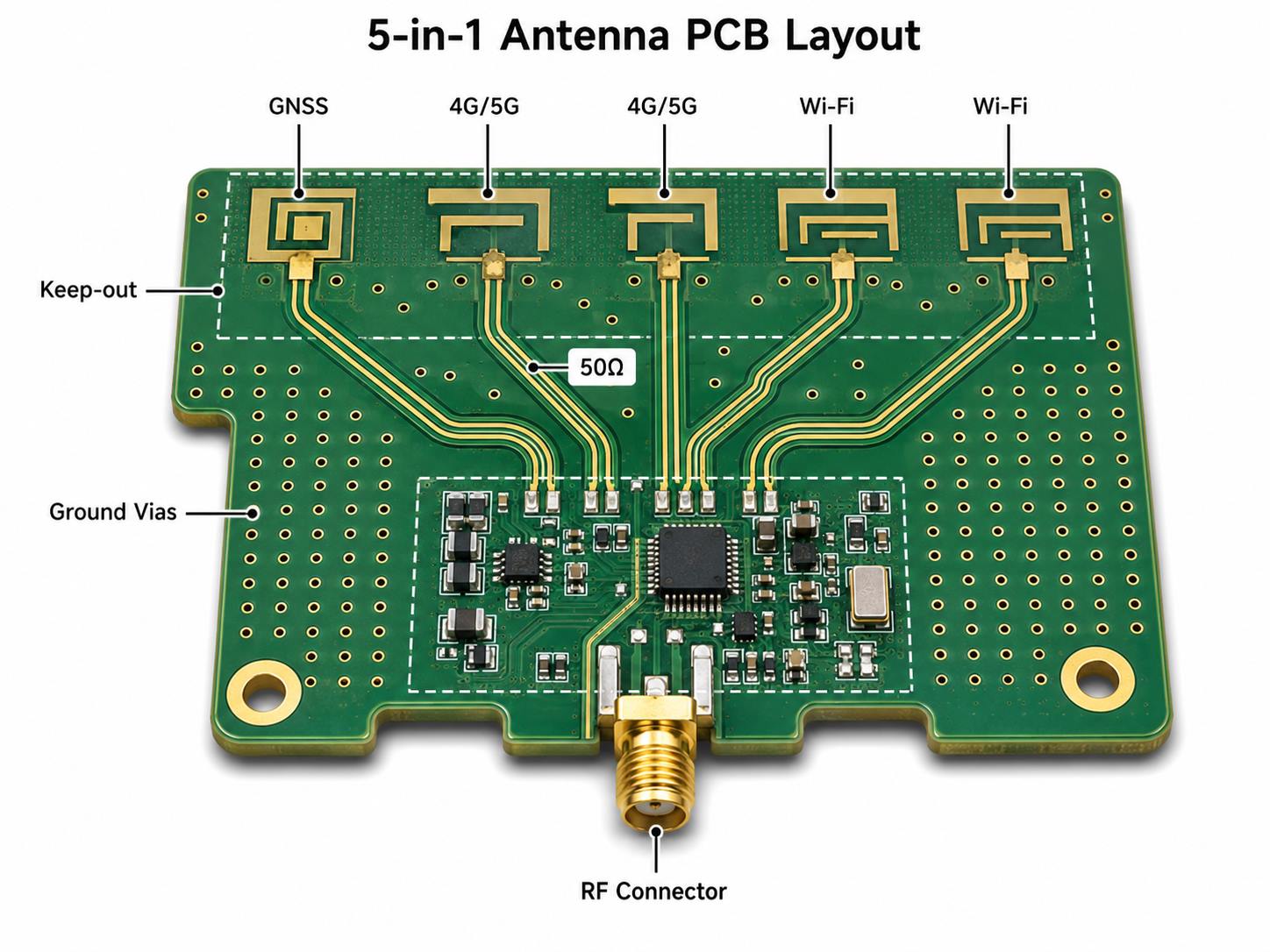
Most GNSS, cellular, and Wi-Fi feed lines use 50Ω controlled impedance. This requirement should be clearly marked in the fabrication notes.
Customers should provide:
- Target impedance
- Controlled impedance layer
- Trace width and spacing
- Stackup drawing
- Impedance tolerance
- Test coupon requirement
Without clear impedance notes, the board may be treated as a normal PCB instead of an RF-controlled board.
3. RF Connector Footprint
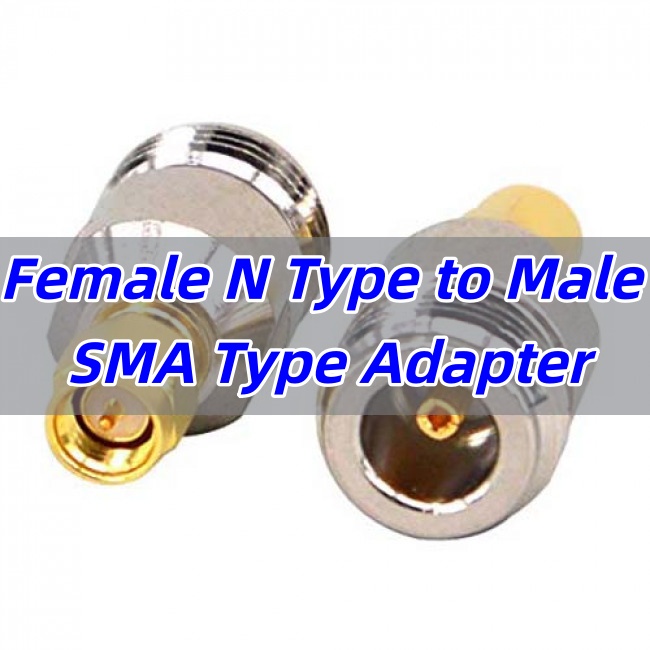
RF connector problems are common in antenna-related PCBA projects. SMA, U.FL, IPEX, MMCX, and board-to-board RF connectors all have specific footprint requirements.
Check:
- Pad size
- Ground pad connection
- Solder mask opening
- Connector orientation
- Edge clearance
- Cable direction
- Rework space
A small footprint error can cause soldering defects, weak contact, or unstable field performance.
RF Connector Area and Assembly Clearance
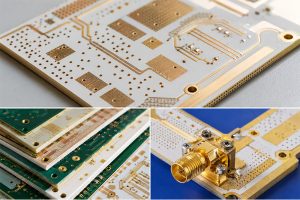
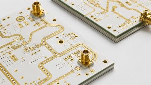
The RF connector area should be reviewed before PCB fabrication and PCBA assembly. For a 5-in-1 antenna product, connector placement and nearby PCB details can affect soldering quality, cable installation, inspection, rework access, and production consistency.
A PCB/PCBA manufacturer can help check whether the connector footprint, solder mask opening, ground pads, board edge clearance, and cable direction match the assembly requirement. If the customer provides a wireless module layout guide or antenna reference design, the manufacturer can also review whether the board files follow the key manufacturing notes.
Check before production:
- RF connector footprint against the datasheet
- Pad size and solder mask opening
- Ground pad connection around the connector
- Board edge clearance
- Cable plugging direction
- Space for manual inspection and rework
- Coaxial cable bend radius
- Shielding can footprint and solderability, if used
- Keep-out notes provided by the module or antenna supplier
This review does not replace antenna tuning, OTA testing, or RF chamber testing. Its purpose is to reduce assembly risk, connector failure, soldering defects, and avoidable layout-to-production problems.
What Types of PCBs Are Used in 5-in-1 Antenna Products?
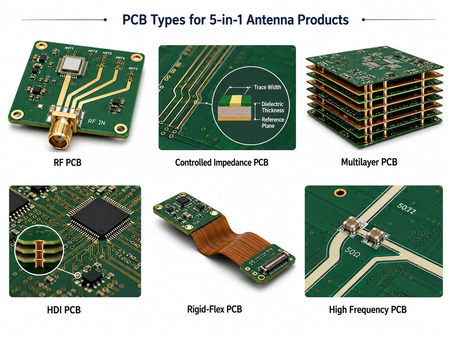
Different products need different PCB structures. The PCB type should match the RF requirement, space limit, assembly method, and working environment.
| PCB Type | Typical Use | Manufacturing Value |
|---|---|---|
| RF PCB | Antenna feed lines, wireless modules | Better RF trace and impedance control |
| High Frequency PCB | Higher-frequency or lower-loss RF paths | More stable signal transmission |
| Controlled Impedance PCB | GNSS, cellular, Wi-Fi RF traces | Keeps 50Ω signal paths consistent |
| Multilayer PCB | Gateways, routers, tracking devices | Better grounding, routing, and power distribution |
| HDI PCB | Compact wireless devices | Supports fine-pitch modules and dense routing |
| Rigid PCB | Industrial and outdoor devices | Stable structure for connectors and modules |
| Flexible PCB | Space-limited internal connections | Fits compact mechanical structures |
| Rigid-Flex PCB | Multi-section compact devices | Reduces connectors and improves reliability |
| High-TG PCB | Automotive, outdoor, industrial products | Better thermal stability |
| Ceramic PCB | Special RF or thermal-sensitive modules | Good for high-reliability applications |
| Metal Core PCB | Smart LED or power products with wireless function | Helps thermal management |
For many projects, the practical choice is a multilayer controlled impedance PCB. Compact products may use HDI PCB or rigid-flex PCB. Higher-frequency paths may require RF PCB or high frequency PCB.
What Should Be Checked During PCBA Assembly?
5-in-1 antenna PCBA assembly usually includes RF connectors, wireless modules, small matching components, shielding parts, and coaxial cables. These areas need tighter process control.
RF Connectors
- Check connector position, solder quality, grounding, mechanical strength, and cable plugging direction. U.FL and IPEX connectors are small and can be damaged by poor soldering or repeated rework.
Wireless Modules
- Check solder paste volume, stencil opening, reflow profile, placement accuracy, and inspection method. LGA, BGA, castellated, and fine-pitch wireless modules need stable SMT control.
Matching Network Components
- Small capacitors and inductors near RF paths must match the BOM and placement file. Wrong values or wrong positions can change RF behavior.
Shielding Cans
- Shielding only works well when grounding and soldering are reliable. Shielding can footprints, solder paste openings, and inspection standards should be confirmed before assembly.
Coaxial Cables and Wire Harnesses
- Cable direction, bend radius, connector locking, strain relief, and final assembly sequence should be checked before batch production.
First Article Inspection
- For the first build, inspect connector placement, module alignment, component value, polarity, solder joints, shielding position, and test results before moving to larger quantities.
What Testing Should Be Planned Before Shipment?
Testing should be defined before assembly, not after production is finished.
| Test | Purpose |
|---|---|
| Bare PCB electrical test | Check opens and shorts |
| Impedance test | Confirm RF trace impedance on test coupon |
| AOI | Check solder joints, polarity, missing parts |
| X-ray | Inspect BGA/LGA or hidden solder joints |
| Functional test | Confirm power, module boot, interface communication |
| RF path continuity check | Find connector or soldering issues |
| GNSS/Wi-Fi/cellular function check | Verify product-level wireless function |
| Final assembly inspection | Check cable, connector, enclosure, label, and package |
A PCB/PCBA factory can support production-level tests such as electrical test, impedance test, AOI, X-ray, visual inspection, and functional testing based on customer procedures.
Advanced antenna tests such as OTA, radiation pattern, antenna efficiency, and certification-level RF performance usually require customer fixtures, RF chambers, or third-party labs.
What Files Are Needed for a Faster Quote?
Complete files help the manufacturer review the project faster and quote more accurately.
Send:
- Gerber or ODB++ files
- Drill files
- PCB stackup
- Controlled impedance requirement
- BOM with manufacturer part numbers
- Pick-and-place file
- Assembly drawing
- RF connector datasheets
- Wireless module datasheets
- Antenna specification
- Testing requirements
- Cable or wire harness requirements
- Order quantity
- Target delivery schedule
For PCBA projects, BOM quality matters. RF connectors, wireless modules, EOL parts, and alternative components should be checked before batch production.
FAQs About 5-in-1 Antenna PCB and PCBA Manufacturing
Q1: Can a PCB/PCBA manufacturer design the 5-in-1 antenna?
Usually no. A PCB/PCBA manufacturer supports layout review, DFM, impedance control, fabrication, assembly, and testing. Full antenna electromagnetic design should be handled by RF antenna specialists.
Q2: Does a 5-in-1 antenna PCB need controlled impedance?
In most cases, yes. GNSS, cellular, and Wi-Fi RF feed lines commonly require 50Ω controlled impedance.
Q3: Can FR4 be used for 5-in-1 antenna products?
Yes, FR4 can be used when the frequency, loss requirement, and layout structure are suitable. For higher-frequency or lower-loss paths, high frequency PCB materials may be needed.
Q4: What is the most common manufacturing issue?
Common issues include unclear impedance notes, incorrect RF connector footprints, poor grounding, missing assembly clearance, wrong matching components, and poor cable routing.
Q5: What PCB type is commonly used?
Many projects use multilayer controlled impedance PCB. Compact wireless products may use HDI PCB or rigid-flex PCB.
Q6: Can the factory test RF performance?
The factory can support production-level tests. Advanced RF performance testing may require customer fixtures, RF chambers, or third-party RF labs.
In summary, a 5-in-1 antenna product is not difficult only because it uses several wireless functions. The real production challenge is making the PCB and PCBA stable, repeatable, and testable.
Before production, customers should confirm RF trace impedance, stackup, connector footprint, assembly clearance, shielding parts, cable routing, BOM accuracy, and test method. These checks help reduce rework, shorten debugging time, and improve batch consistency.
Best Technology supports RF PCB, high frequency PCB, controlled impedance PCB, multilayer PCB, HDI PCB, rigid-flex PCB, ceramic PCB, metal core PCB, PCB fabrication, PCBA assembly, SMT stencil, wire harness, component sourcing, DFM review, and production testing.
Send your Gerber files, BOM, antenna specification, and project requirements to sales@bestpcbs.com. Our engineering team can review your 5-in-1 antenna PCB and PCBA project before production and help you move from prototype to a more stable manufacturing build.