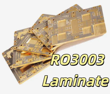
How to achieve optimal high-frequency performance and PCB power integrity through RF PCB materials selection while balancing performance, cost and practicality? This guide clarifies core material factors, resolves related selection issues, and delivers actionable solutions for stable signal integrity and reliable power delivery.
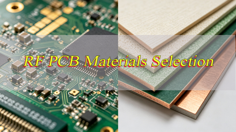
Why Is RF PCB Materials Selection Critical for High-Frequency Signal Integrity?
RF PCB materials directly determine how well high-frequency signals travel through the board, and their impact on PCB power integrity cannot be overstated. High-frequency signals, typically above 1 GHz, are extremely sensitive to substrate properties. Even minor inconsistencies in material composition can cause signal attenuation, reflection, or crosstalk. All of these issues disrupt both signal integrity and PCB power integrity.
Poor material selection leads to increased signal loss. This forces devices to consume more power to maintain performance, reducing energy efficiency and straining power delivery systems. Ultimately, this compromises PCB power integrity. For example, a substrate with unstable dielectric properties can cause impedance mismatches. These mismatches lead to signal reflections that distort data transmission and create power fluctuations across the PCB.
In high-frequency applications like 5G, aerospace, and microwave systems, PCB power integrity is non-negotiable. These systems rely on consistent power delivery to support high data rates and reliable operation. Choosing the wrong material can result in costly rework, product failures, and reduced device lifespan. These issues are avoidable with informed material selection focused on both signal integrity and PCB power integrity.
What Factors Matter in RF PCB Materials Selection for High-Frequency Stability?
Selecting materials for RF PCBs requires balancing multiple interconnected factors. These factors directly influence high-frequency stability and PCB power integrity. No single factor stands alone. Each contributes to overall performance, and overlooking any can lead to systemic issues. Below are the most critical considerations, explained clearly for practical use.
- Dielectric Constant (Dk): A stable, low dielectric constant is essential for high-frequency stability. Dk values must remain consistent across temperature, frequency, and humidity to prevent impedance drift. Impedance drift disrupts both signal flow and PCB power integrity. Materials with erratic Dk values cause signal reflections and power inconsistencies.
- Dielectric Loss (Df): Also known as loss tangent, Df measures energy dissipation in the substrate. Lower Df values minimize signal attenuation and reduce power waste. This directly supports PCB power integrity. High Df materials convert signal energy to heat, straining power systems and degrading performance.
- Thermal Conductivity: High-frequency RF PCBs generate significant heat that must be dissipated efficiently. Materials with high thermal conductivity prevent overheating. Overheating can damage components and destabilize power delivery, undermining PCB power integrity. Thermal management directly impacts long-term stability.
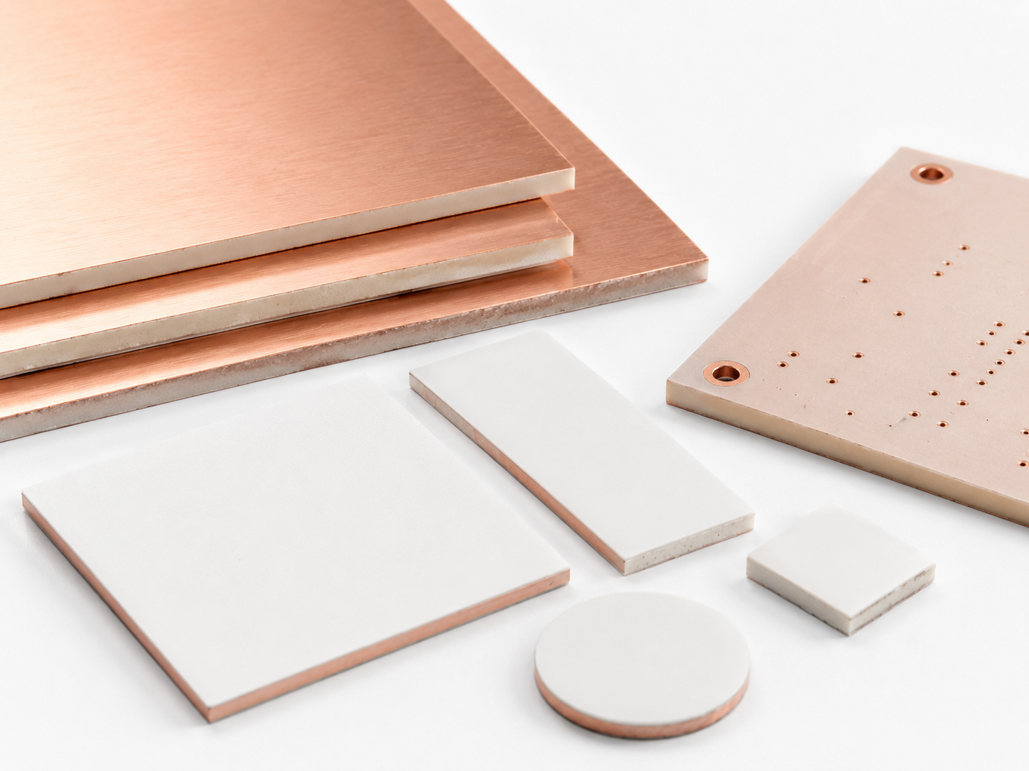
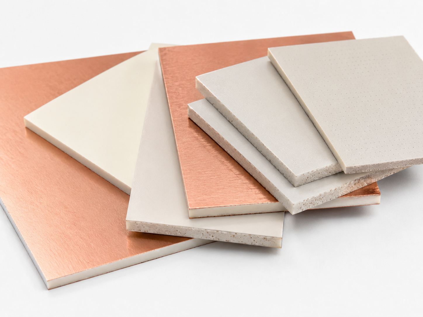
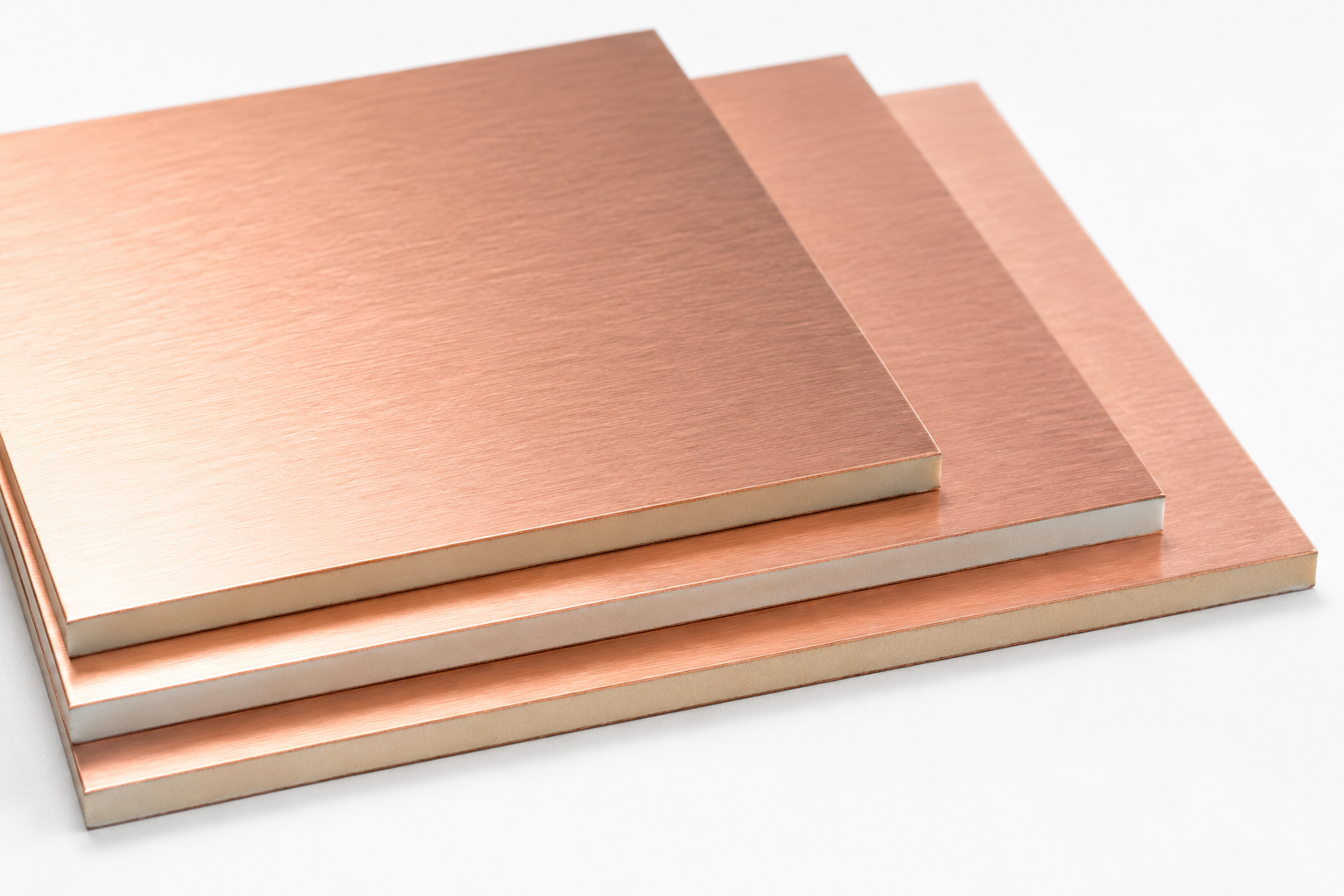
- Copper Foil Quality: Copper foil roughness and thickness affect signal propagation and power distribution. Smooth, low-profile copper reduces signal loss and ensures uniform power delivery. This is critical for maintaining PCB power integrity. Thicker copper improves current-carrying capacity, supporting stable power flow.
- Moisture Absorption: Materials that absorb moisture experience degraded dielectric properties and reduced thermal stability. Moisture absorption increases Dk and Df values, disrupts signal integrity, and weakens PCB power integrity. This is especially true in harsh environments like aerospace or industrial settings.
How Does Dielectric Constant Impact RF PCB Materials Selection?
Dielectric constant (Dk) measures a material’s ability to store electrical energy. It has a direct, measurable impact on RF PCB performance and PCB power integrity. For high-frequency applications, Dk stability and value are non-negotiable. Even small variations can render a design ineffective. Below is a breakdown of how Dk influences material selection and practical considerations for each scenario.
- Dk Value and Signal Speed: Signal speed in a PCB is inversely proportional to the square root of Dk. Lower Dk values (2.2–3.5) enable faster signal propagation. This is critical for high-data-rate applications like 5G and microwave systems. Higher Dk materials slow signals, increasing latency and disrupting timing. This strains PCB power integrity by requiring more power to compensate.
- Dk Stability Across Conditions: The most reliable RF PCB materials maintain consistent Dk values across temperature (–40°C to 125°C), frequency, and humidity. Materials with unstable Dk cause impedance mismatches. These mismatches lead to signal reflections and power fluctuations that harm PCB power integrity. For example, a material with Dk that shifts by 0.5 over operating temperatures can cause a 10% impedance change.
- Dk Matching for Impedance Control: Impedance control (typically 50Ω or 75Ω for RF applications) relies on precise Dk values. Material selection must align with design impedance requirements. Choosing a material with the wrong Dk forces designers to adjust trace width or dielectric thickness. This increases complexity and the risk of power distribution issues that affect PCB power integrity.
- Application-Specific Dk Requirements: Low-frequency RF applications (1–2 GHz) can tolerate slightly higher Dk values (3.5–4.5). High-frequency (20+ GHz) and millimeter-wave applications require low Dk materials (2.2–3.0) to minimize signal loss and maintain PCB power integrity. Matching Dk to application frequency is key to avoiding performance failures.
How Does Thermal Conductivity Affect RF PCB Materials Selection?
Thermal conductivity measures a material’s ability to transfer heat. It is a critical factor in RF PCB materials selection, directly linked to component longevity, signal stability, and PCB power integrity. High-frequency RF circuits generate significant heat from signal dissipation and component operation. Poor thermal conductivity traps heat, causing component damage and performance degradation. This section details how thermal conductivity influences material choices and practical selection solutions.
- Heat Dissipation and Component Reliability: Materials with high thermal conductivity (≥1 W/m·K) efficiently transfer heat from hot components to heat sinks or the PCB edge. This prevents component overheating, which can degrade performance, shorten lifespan, and cause power delivery instability. All of these issues harm PCB power integrity. Low thermal conductivity materials (≤0.3 W/m·K) trap heat, leading to thermal runaway.
- Thermal Expansion Matching: Thermal conductivity is closely tied to the coefficient of thermal expansion (CTE). Materials with mismatched CTE to copper foil or components cause mechanical stress. This stress leads to cracks, delamination, and broken connections. It disrupts signal flow and breaks power paths, severely compromising PCB power integrity.
- Application-Specific Thermal Needs: High-power RF applications (e.g., aerospace transmitters, 5G base stations) require materials with high thermal conductivity (e.g., aluminum nitride, copper-clad laminates) to manage extreme heat. Low-power applications (e.g., consumer RF devices) can use lower thermal conductivity materials. Even so, they must still maintain enough heat transfer to protect PCB power integrity.
- Balancing Thermal Conductivity and Cost: High thermal conductivity materials often cost more than standard options. Designers must balance thermal needs with budget. For example, using a mid-range thermal conductivity material (0.8–1.2 W/m·K) for moderate-power applications can maintain PCB power integrity without excessive cost.
How Do RF PCB Material Selection & Impedance Control Challenges Affect Signal Integrity?
Impedance control is critical for RF PCB signal integrity. Material selection directly impacts both impedance stability and PCB power integrity. Inconsistent material properties (e.g., Dk, thickness) cause impedance mismatches. These mismatches lead to signal reflections, attenuation, and power waste. This section explains their interaction and how to mitigate these issues.
- Material Inconsistencies Cause Impedance Drift: Variations in Dk, dielectric thickness, or copper foil roughness across a PCB lead to uneven impedance. This causes signal reflections that distort data. It also forces power systems to work harder to maintain signal strength, undermining PCB power integrity. Consistent material properties are essential for stable impedance.
- Dielectric Thickness and Impedance: Impedance is inversely proportional to dielectric thickness. Thicker dielectrics reduce impedance, while thinner dielectrics increase it. Material selection must account for dielectric thickness tolerance. Materials with poor thickness consistency create impedance hotspots. These hotspots disrupt signal flow and power distribution, which harms PCB power integrity.
- Copper Foil Roughness and Signal Loss: Rough copper foil increases signal loss (skin effect) and can alter effective Dk. This leads to impedance mismatches. Smooth, low-profile copper foil minimizes these issues. It ensures consistent impedance and reduces power waste, directly supporting PCB power integrity. Material selection should prioritize copper quality for high-frequency designs.
- Mitigating Impedance Challenges with Material Choice: Selecting materials with tight Dk and thickness tolerances reduces impedance drift. For example, polytetrafluoroethylene (PTFE) materials offer stable Dk and low loss. This makes them ideal for high-frequency designs requiring precise impedance control and reliable PCB power integrity.
How to Choose Substrates in RF PCB Materials Selection to Reduce Signal Loss?
Signal loss is the primary enemy of high-frequency RF PCBs. Substrate selection is the most effective way to minimize it while also supporting PCB power integrity. Signal loss occurs through dielectric absorption, conductor loss, and radiation. All of these are directly influenced by substrate properties. Below are actionable steps to choose substrates that reduce signal loss and maintain PCB power integrity.
- Prioritize Low Dielectric Loss (Df): Substrates with low Df values (≤0.004) minimize dielectric absorption. This is the main source of signal loss in high-frequency applications. Materials like PTFE, hydrocarbon ceramics, and liquid crystal polymer (LCP) offer low Df. They reduce signal attenuation and power waste, which is critical for maintaining PCB power integrity.
- Select Stable Dielectric Constant (Dk): Substrates with consistent Dk values across frequency and temperature prevent impedance mismatches. These mismatches cause signal reflections and loss. Avoid materials with Dk variations greater than ±0.1. These variations lead to unpredictable signal behavior and strain power delivery systems, harming PCB power integrity.
- Opt for Smooth Copper Foil: Conductor loss increases with copper foil roughness due to the skin effect. Low-profile or ultra-low-profile copper foil (roughness ≤1.5 μm) reduces conductor loss. This ensures more signal reaches its destination and reduces power consumption, directly supporting PCB power integrity.
- Choose Low Moisture Absorption Materials: Moisture increases Dk and Df values, leading to higher signal loss and degraded PCB power integrity. Substrates with moisture absorption ≤0.05% (e.g., PTFE, LCP) maintain performance in humid environments. They prevent signal loss and power instability.
- Match Substrate to Frequency: Low-frequency RF (1–5 GHz) can use cost-effective substrates like modified FR4 with low Df. High-frequency (5+ GHz) and millimeter-wave applications require advanced substrates (PTFE, LCP) to minimize loss and protect PCB power integrity.
What to Consider for RF Microwave Millimeter-Wave PCB Material Selection?
RF microwave and millimeter-wave applications (24 GHz and above) demand the highest performance from PCB materials. Signal loss and impedance drift are amplified at these frequencies. Material selection for these applications must prioritize ultra-low loss, stable dielectric properties, thermal management, and PCB power integrity. Below are key selection considerations.
- Ultra-Low Dielectric Loss (Df ≤ 0.002): Millimeter-wave signals are extremely sensitive to dielectric loss. Materials like PTFE and LCP with Df values ≤0.002 minimize signal attenuation. This ensures reliable communication and reduces power waste, which is critical for maintaining PCB power integrity in high-frequency systems.
- Stable Dk Across Wide Frequency Ranges: Millimeter-wave applications span multiple frequency bands. Substrates must maintain consistent Dk (±0.05) across these ranges. Unstable Dk causes impedance mismatches, signal reflections, and power fluctuations that harm PCB power integrity.
- Thermal Management for High Power Density: Millimeter-wave components often have high power density, generating significant heat. Substrates with high thermal conductivity (≥1.5 W/m·K) and low CTE (matched to copper) prevent overheating and mechanical stress. This protects both signal integrity and PCB power integrity.
- Low Surface Roughness Copper: Ultra-low-profile copper foil (roughness ≤0.4 μm) is essential for millimeter-wave PCBs. Rough copper increases conductor loss and alters effective Dk. This leads to signal degradation and power inefficiency, undermining PCB power integrity.
- Mechanical Stability: Millimeter-wave PCBs often have fine traces and tight tolerances. Substrates must have high mechanical strength to withstand manufacturing processes (e.g., drilling, etching) without warping or cracking. Warping or cracking would disrupt signal paths and power delivery, harming PCB power integrity.
How to Balance Cost & Performance in RF PCB Materials Selection?
Balancing cost and performance is a common challenge in RF PCB materials selection. High-performance materials often come with higher price tags. The goal is to select materials that meet performance requirements without overspending. This also means maintaining PCB power integrity and signal stability. Below are practical strategies to achieve this balance.
- Match Material Performance to Application Requirements: Avoid over-specifying materials. For low-frequency RF applications (≤1 GHz), use cost-effective modified FR4 (low Df variant) instead of expensive PTFE. For high-frequency applications (5+ GHz), invest in RF-specific materials to ensure PCB power integrity and signal performance. Cut costs elsewhere (e.g., trace design) if needed.
- Use Hybrid Substrate Designs: Hybrid PCBs combine high-performance materials (e.g., PTFE) for critical RF signal layers with lower-cost materials (e.g., FR4) for power and ground layers. This approach maintains PCB power integrity and signal quality where it matters most. It also reduces overall material costs by up to 30%.
- Optimize Material Thickness and Copper Weight: Thicker dielectrics and copper foil increase costs. Select the minimum thickness and copper weight that meet performance requirements. For example, use 1 oz copper instead of 2 oz for low-power RF applications. This reduces material costs without compromising PCB power integrity or signal loss.
- Work with Reliable Suppliers: Reputable suppliers offer consistent material quality. This reduces the risk of rework and waste. While some suppliers may offer lower prices, inconsistent material properties can lead to performance failures, increased costs, and compromised PCB power integrity. Reliable suppliers are a cost-effective choice long-term.
- Consider Volume and Lead Time: Ordering materials in volume often reduces per-unit costs. For high-volume production, negotiate with suppliers for bulk discounts. For low-volume prototypes, use cost-effective alternatives (e.g., modified FR4) to test designs before investing in high-performance materials. This ensures PCB power integrity is maintained in final production.
What Mistakes to Avoid in RF PCB Board Material Selection?
Even experienced designers make mistakes in RF PCB materials selection. These mistakes often lead to poor performance, increased costs, and compromised PCB power integrity. They are avoidable with careful planning and attention to application requirements. Below are the most common mistakes and how to avoid them.
- Choosing Materials Based on Cost Alone: Prioritizing low cost over performance leads to materials with unstable Dk, high Df, and poor thermal conductivity. This causes signal loss, impedance mismatches, and power instability. It harms PCB power integrity and requires costly rework. Always match material performance to application needs first.
- Ignoring Moisture Absorption: Overlooking moisture absorption leads to degraded dielectric properties over time. This is especially true in humid environments. Materials with high moisture absorption (e.g., standard FR4) experience increased Dk and Df. This leads to signal loss and compromised PCB power integrity. Select materials with moisture absorption ≤0.05% for reliable performance.
- Overlooking Thermal Conductivity: Failing to consider thermal conductivity leads to overheating, component damage, and power delivery instability. High-frequency RF PCBs generate significant heat. Materials with low thermal conductivity trap heat, undermining PCB power integrity and shortening device lifespan. Always match thermal conductivity to power requirements.
- Neglecting Impedance Control Tolerances: Selecting materials with loose Dk or thickness tolerances causes impedance drift. This leads to signal reflections and power waste. It harms PCB power integrity and reduces signal quality. Choose materials with tight tolerances (Dk ±0.05, thickness ±5%) for precise impedance control.
- Using FR4 for High-Frequency Applications: As discussed earlier, FR4 is unsuitable for frequencies above 1 GHz. Using FR4 in high-frequency designs leads to excessive signal loss, impedance mismatches, and unstable PCB power integrity. Always select RF-specific materials for applications above 1 GHz.
FAQs About RF PCB Material Selection
Q1: What is the best material for high-frequency RF PCBs that need to maintain PCB power integrity?
A1: The best material depends on frequency and application, but PTFE, hydrocarbon ceramics, and LCP are top choices. These materials offer low Dk, low Df, and stable properties. They minimize signal loss and support reliable PCB power integrity. PTFE is ideal for millimeter-wave applications, while hydrocarbon ceramics balance performance and cost for 5G systems.
Q2: Can modified FR4 be used for 5G RF PCBs without compromising PCB power integrity?
A2: Modified FR4 (low Df variant) can be used for low-frequency 5G applications (≤3 GHz) with minimal power requirements. For high-frequency 5G (≥3 GHz), modified FR4 lacks the stable dielectric properties needed to maintain PCB power integrity. RF-specific materials like PTFE or LCP are recommended instead.
Q3: How does copper foil roughness affect PCB power integrity in RF PCBs?
A3: Copper foil roughness increases conductor loss due to the skin effect, which wastes power and degrades signal quality. Smooth, low-profile copper foil reduces loss. It ensures more power reaches components and maintains stable PCB power integrity. Ultra-low-profile copper is essential for millimeter-wave applications.
Q4: What moisture absorption level is acceptable for RF PCB materials to protect PCB power integrity?
A4: Materials with moisture absorption ≤0.05% are ideal for RF PCBs. Higher moisture absorption increases Dk and Df, leading to signal loss and power instability. This harms PCB power integrity. PTFE and LCP have moisture absorption levels well below 0.05%, making them suitable for harsh environments.
Q5: How do I balance cost and PCB power integrity when selecting RF PCB materials?
A5: Use hybrid substrate designs, matching material performance to application needs. Use high-performance materials for critical RF layers and lower-cost materials for power/ground layers. Avoid over-specifying materials, optimize thickness/copper weight, and work with reliable suppliers. This reduces waste and maintains PCB power integrity without overspending.