PCB manufacturing PCB manufacturing
Home > Blog

Ceramic PCB vs FR4: Which PCB Material Should You Choose?

May 13th, 2026

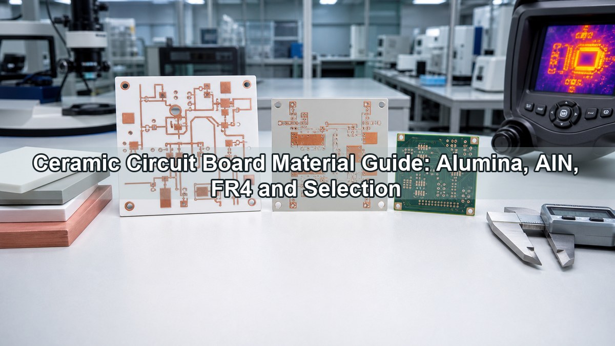
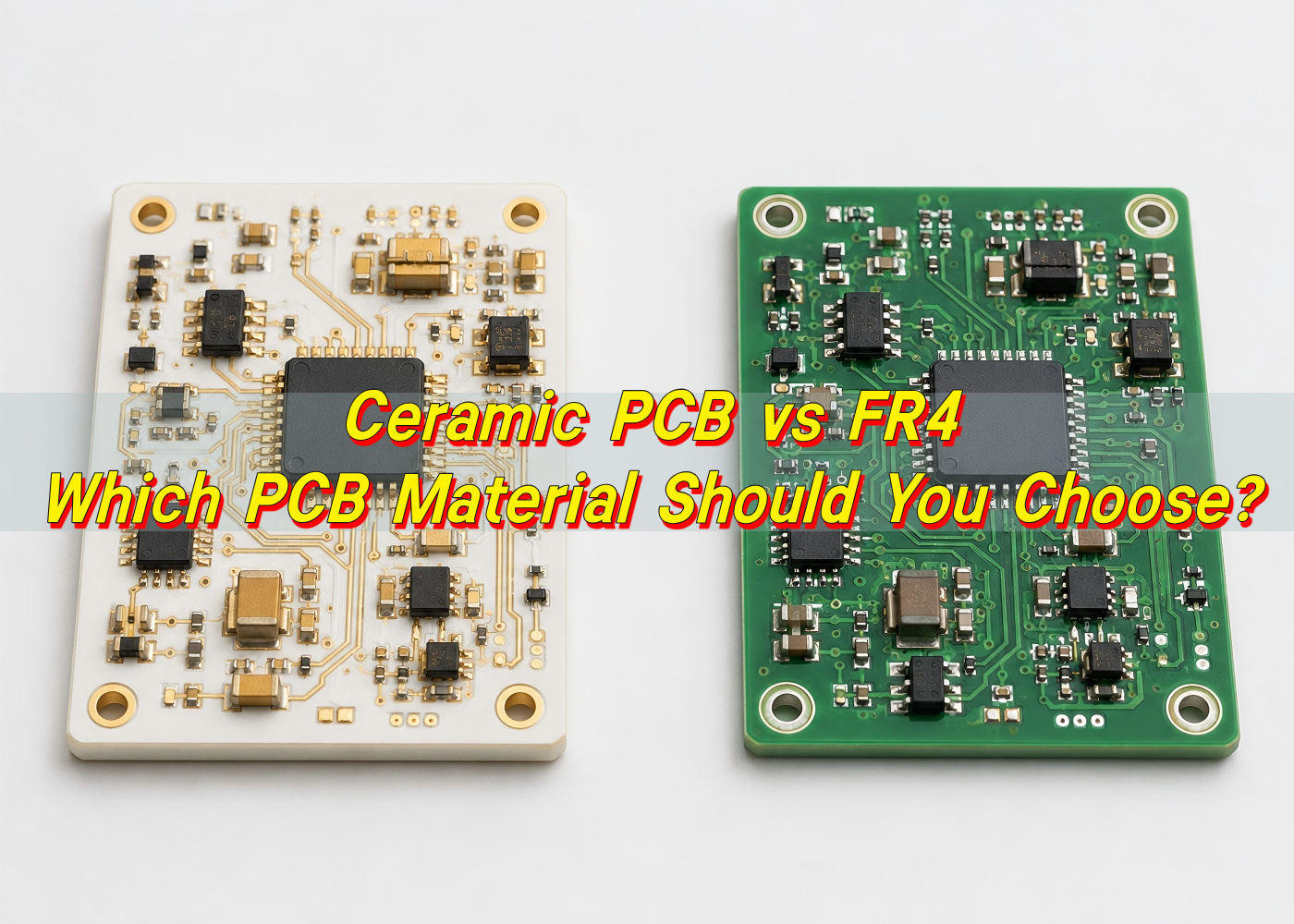
Choosing between ceramic PCB VS FR4 PCB is not only a material decision. It affects heat flow, electrical stability, board thickness, cost, lead time, assembly reliability, and long-term product performance. For many standard electronic products, FR4 is practical, proven, and cost-friendly. For high-power, high-temperature, high-frequency, or high-reliability designs, ceramic PCB can offer a stronger technical foundation.
Ceramic PCB vs FR4: Which PCB Material Should You Choose?

At EBest Circuit (Best Technology), we usually recommend customers review the application first, not the material name first. Heat, voltage, frequency, size, reliability target, assembly method, and production volume should guide the decision. Once these points are clear, the comparison becomes much easier.

What Is a Ceramic PCB?

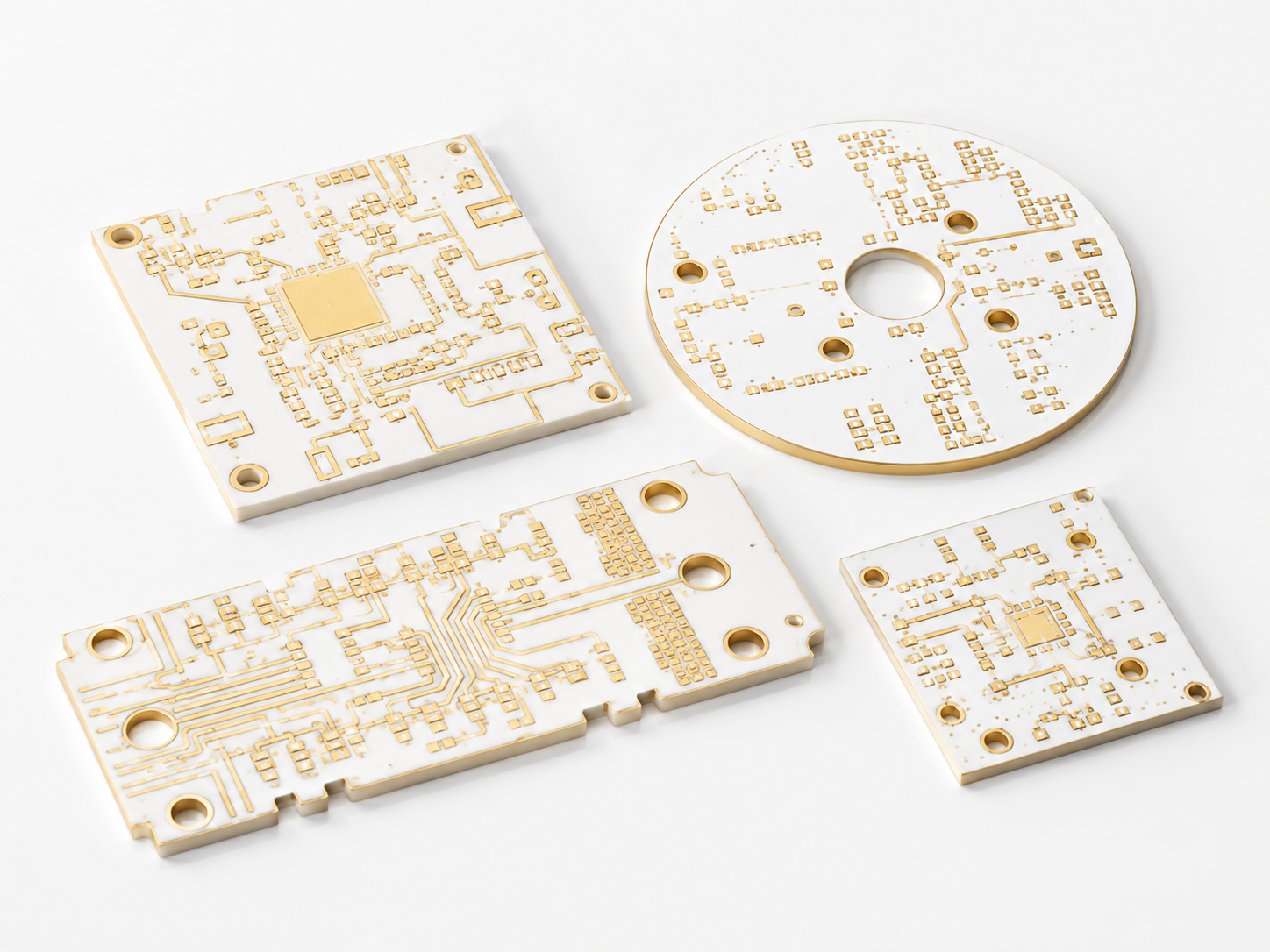
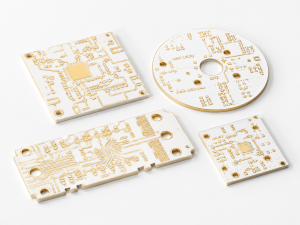
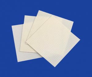
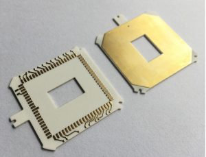
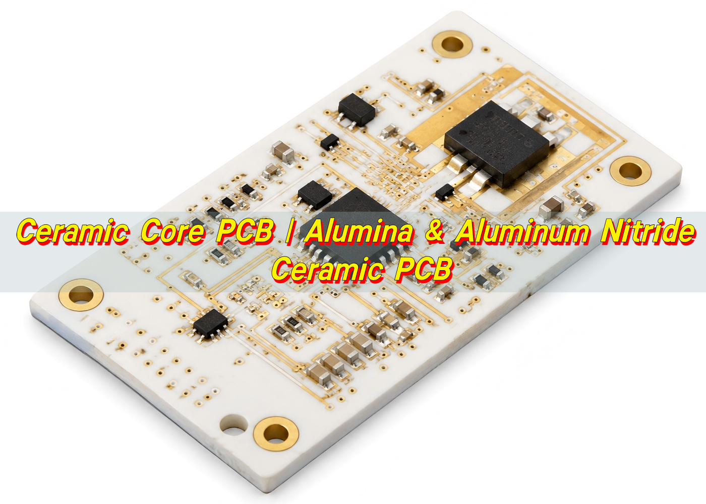
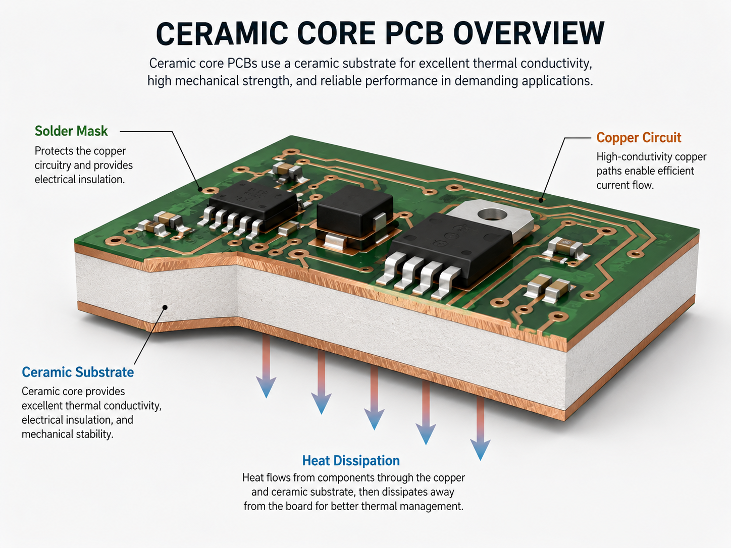
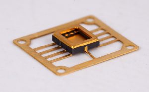
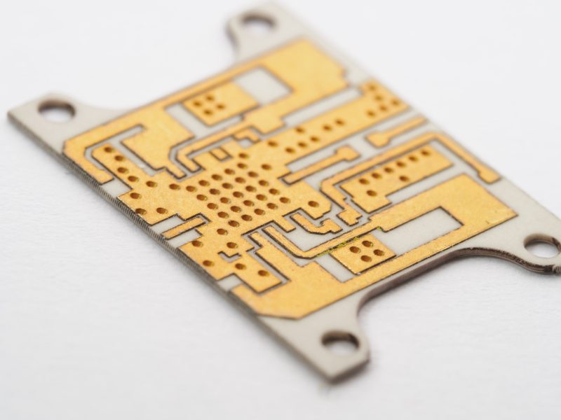
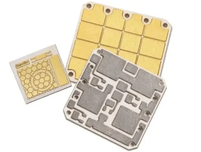
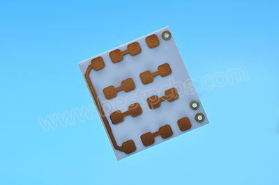
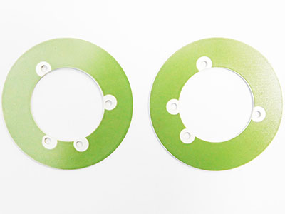
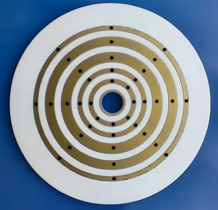
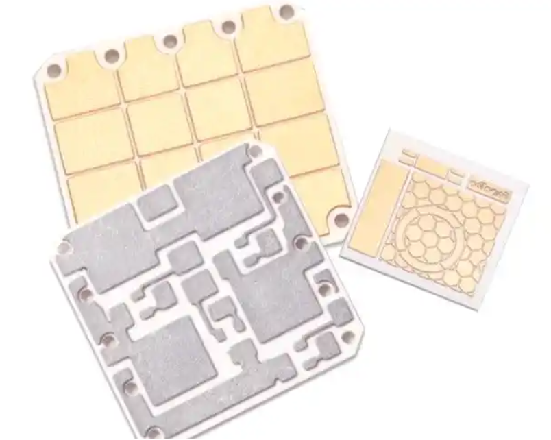
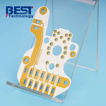
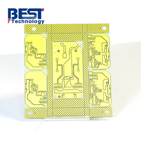
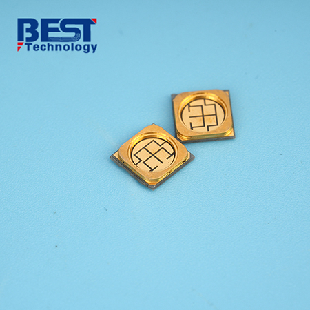
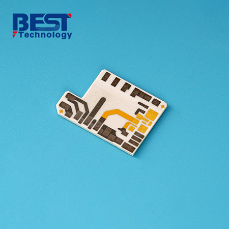
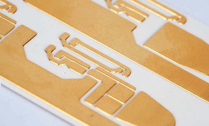
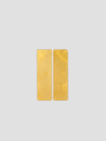
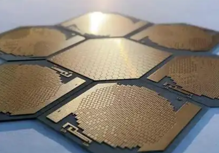
Ceramic PCB is a printed circuit board that uses a ceramic substrate instead of a traditional glass-reinforced epoxy base. The most common ceramic PCB materials include alumina, aluminum nitride, and sometimes silicon nitride. These materials are selected because they provide excellent thermal conductivity, strong electrical insulation, stable mechanical properties, and reliable performance under demanding conditions.

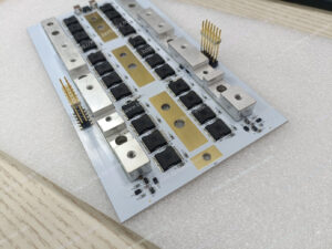
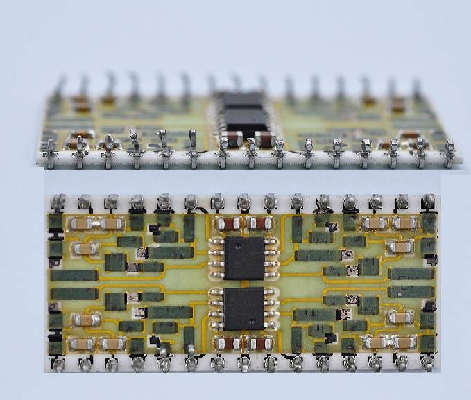
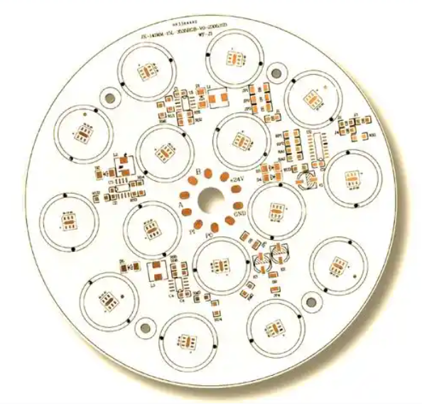
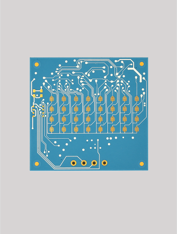
Ceramic PCBs are widely used in high-power LED modules, power electronics, RF circuits, semiconductor packaging, laser systems, medical equipment, sensor modules, and automotive electronics. These applications often need compact layouts and steady performance over long service life.

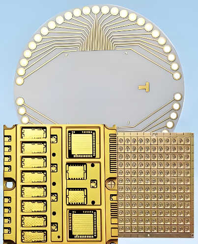
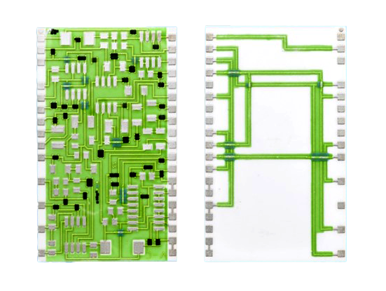
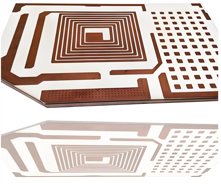
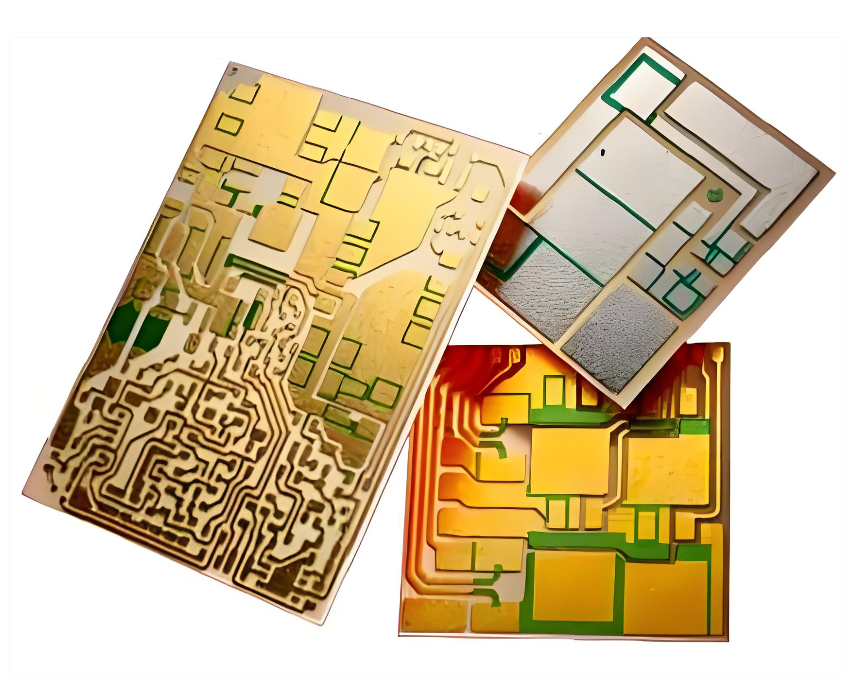
Common ceramic PCB manufacturing processes include thick film, thin film, direct plated copper, direct bonded copper, and active metal brazing. Each process has its own copper thickness range, bonding strength, line width capability, and cost level. For example, DPC ceramic PCBs are suitable for fine circuits and precision applications, while DBC and AMB ceramic substrates are often used for high-current and power module designs.

A ceramic PCB is often chosen when engineers need:

  • Better heat transfer from components to the substrate
  • Stable electrical insulation under high voltage or high temperature
  • Good dimensional stability for precision circuits
  • Long service life in harsh environments
  • Compact packaging for high-density power or RF designs

What Is an FR4 PCB?

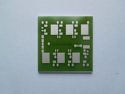
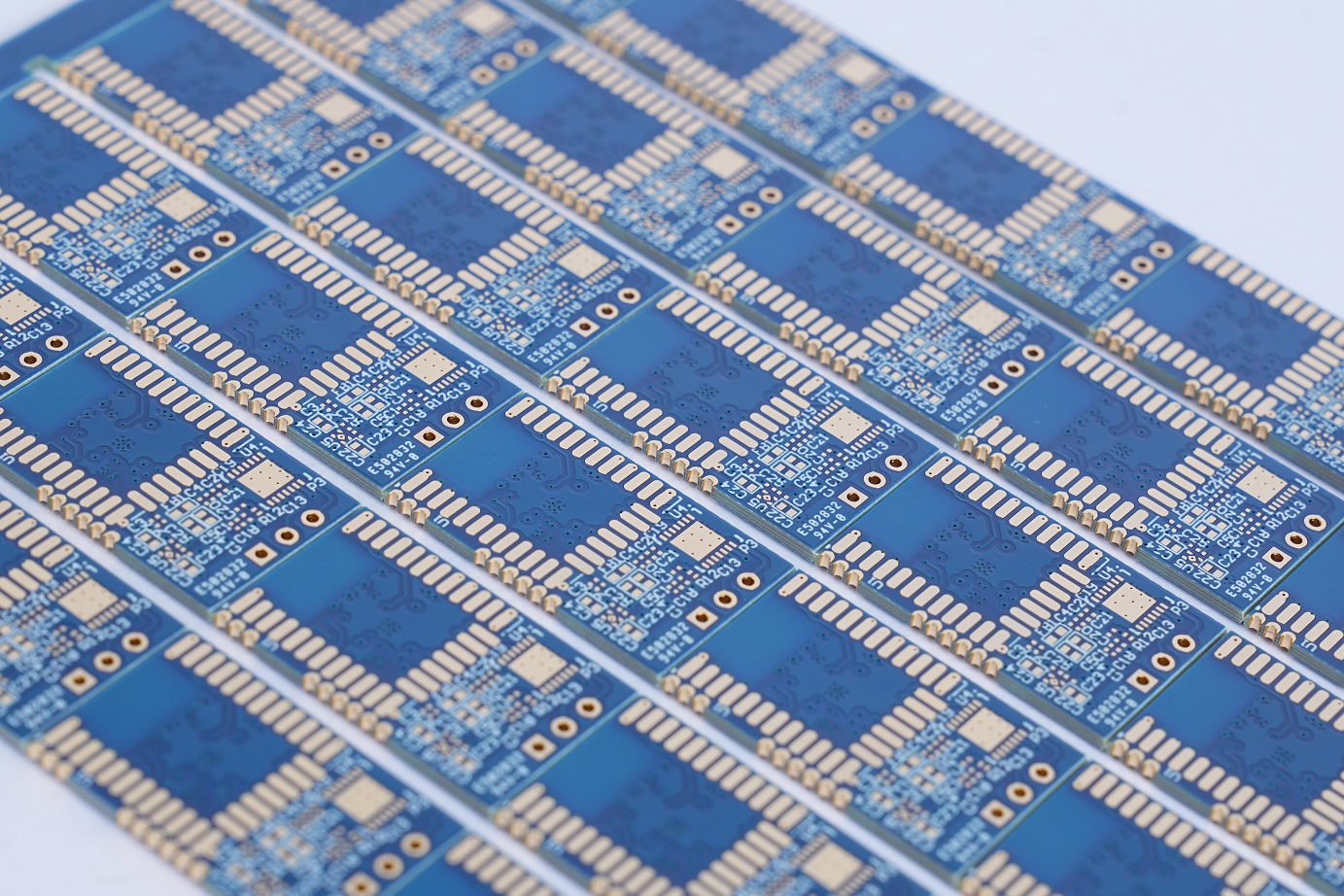
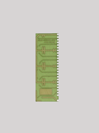
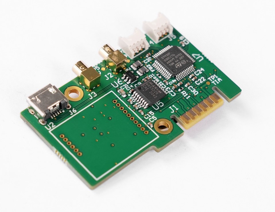
An FR4 PCB is the most widely used type of printed circuit board in the electronics industry. FR4 refers to a glass fiber reinforced epoxy laminate. It acts as the insulating base material that supports copper circuits, solder mask, silkscreen, plated holes, and electronic components.

FR4 became popular because it offers a strong balance of performance, availability, manufacturability, and cost. It is easy to process, suitable for single-sided, double-sided, and multilayer boards, and compatible with most standard PCB fabrication and PCBA assembly workflows.

The key strength of FR4 is its versatility. It can support simple low-cost boards and advanced multilayer designs. Designers can select different Tg grades, copper weights, thicknesses, and finishes based on the application. High-Tg FR4 materials are also available for products that require better thermal resistance during soldering and operation.

FR4 PCB is commonly used for:

  • Control boards
  • Consumer electronics
  • Industrial automation circuits
  • Power supply control sections
  • Communication modules
  • IoT and smart devices
  • General LED driver boards
  • Automotive signal and control electronics

FR4 is a dependable choice when the board does not need extreme thermal conductivity from the base material. It can still handle many thermal designs through copper thickness, thermal vias, heat sinks, metal enclosures, and proper layout strategy. For many projects, this makes FR4 the most practical starting point.

Ceramic PCB vs FR4: What Is the Main Difference?

The main difference between ceramic PCB and FR4 PCB is the substrate material. Ceramic PCB uses a ceramic base with higher thermal conductivity, better dimensional stability, and stronger high-temperature performance. FR4 PCB uses glass fiber epoxy laminate, which is easier to manufacture, more flexible in multilayer design, and more cost-effective for general electronics.
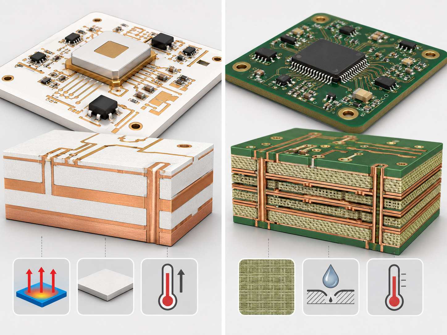
Ceramic PCB vs FR4: Which PCB Material Should You Choose?

A clear comparison helps explain the practical difference:

Comparison ItemCeramic PCBFR4 PCB
Base materialAlumina, aluminum nitride, silicon nitride, or other ceramic substrateGlass fiber reinforced epoxy laminate
Main strengthThermal conductivity, insulation, stability, reliabilityCost efficiency, routing flexibility, broad availability
Typical thermal conductivityMuch higher, depending on ceramic materialLower, usually around standard epoxy laminate levels
High-temperature behaviorExcellent stability in demanding environmentsGood for standard electronics, improved with high-Tg material
Mechanical behaviorHard and dimensionally stableStrong, process-friendly, and more forgiving
Multilayer routingAvailable, but process depends on ceramic technologyVery mature and widely used
Fine circuit capabilityStrong with DPC or thin-film processStrong with HDI and advanced FR4 fabrication
Cost levelHigherLower
Best fitPower, RF, LED, medical, automotive, aerospace, high-heat modulesGeneral electronics, control boards, digital circuits, cost-sensitive products

In everyday engineering terms, FR4 is the reliable workhorse, while ceramic PCB is the performance-focused material for tougher electrical and thermal requirements. A well-designed FR4 board can serve many products beautifully. A ceramic board becomes valuable when ordinary thermal paths or insulation strategies are no longer enough.

EBest Circuit often helps customers review this point during DFM evaluation. Sometimes a customer asks for ceramic PCB because they believe it is always better. After checking the power, thermal path, size, and cost target, FR4 may be enough.

How Does Ceramic PCB vs FR4 Compare in Thermal Conductivity?

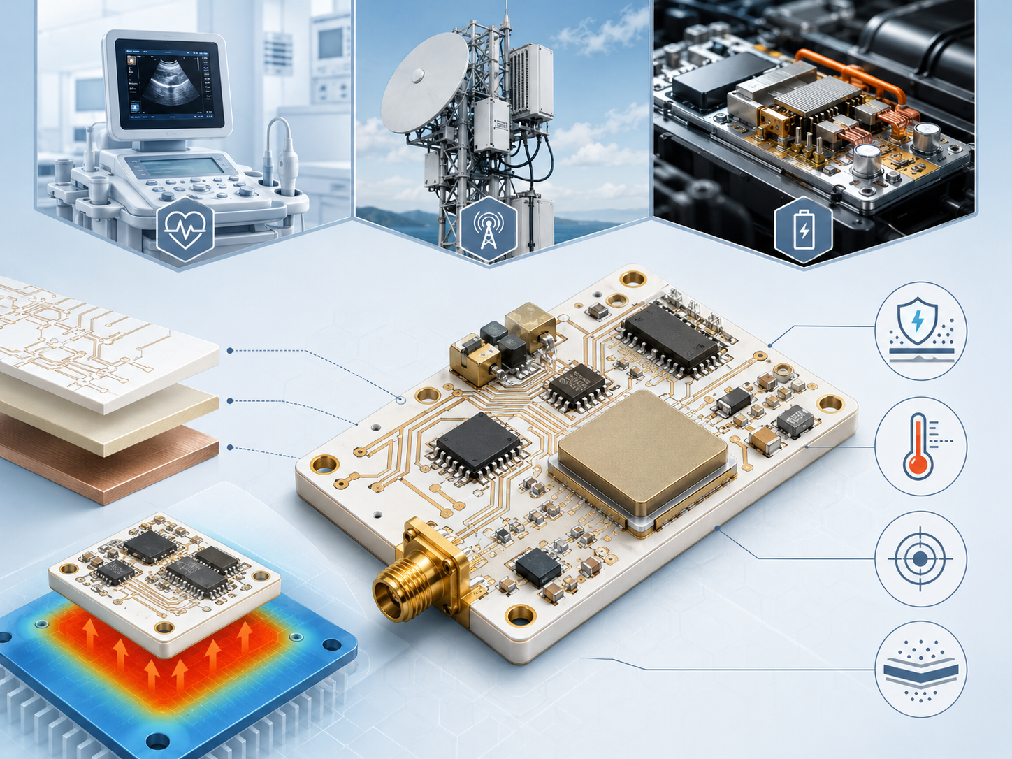
Thermal conductivity is one of the most important reasons engineers compare ceramic PCB vs FR4. Ceramic substrates conduct heat much better than standard FR4 materials. This allows heat generated by LEDs, power semiconductors, RF devices, and high-current components to move more efficiently through the board.

Here is a practical comparison:

Material TypeTypical Thermal Conductivity RangePractical Meaning
Standard FR4Around 0.3 W/m·KSuitable for general electronics with moderate heat
High-performance FR4 variantsHigher than standard FR4, but still limited compared with ceramicsUseful when better thermal resistance is needed without changing board family
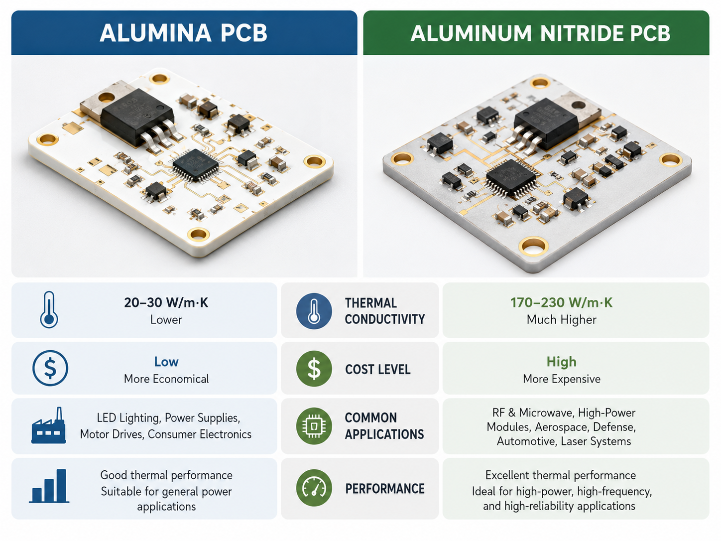
Alumina ceramic PCBCommonly around 20–30 W/m·KStrong option for LED, sensors, power modules, and stable insulation
Aluminum nitride ceramic PCBCommonly around 150–180 W/m·K or higher depending on gradeExcellent choice for high-power and high-heat-density applications
Silicon nitride ceramic PCBStrong thermal and mechanical performance depending on gradeSuitable for advanced power modules and demanding environments

Thermal conductivity should be considered together with copper thickness, component package, solder layer, interface material, enclosure design, and airflow. A material with high conductivity can still perform poorly if the heat path is interrupted.

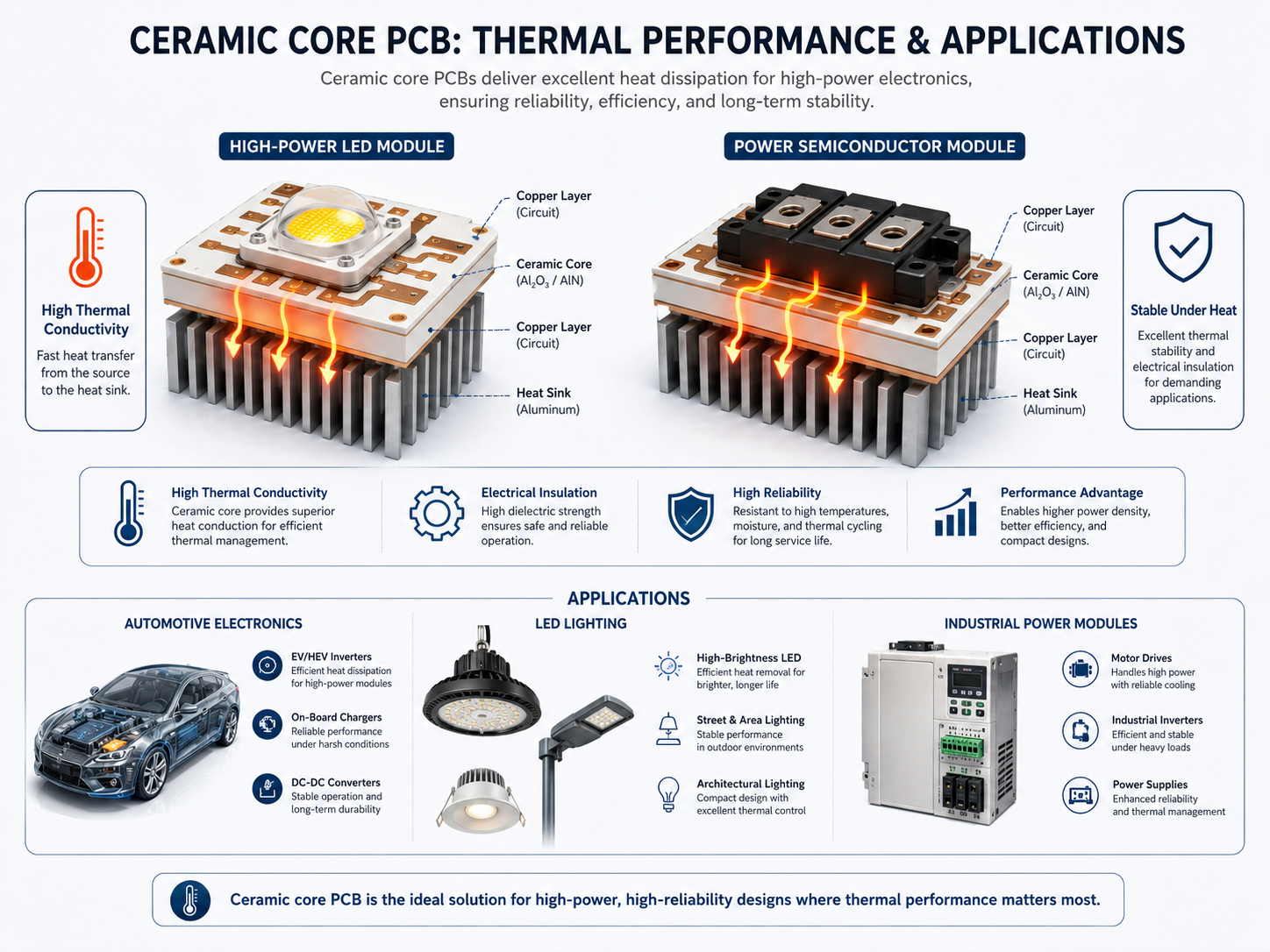
For LED lighting, ceramic PCB can help maintain lower junction temperature, which supports brightness stability and product life. For power electronics, it helps spread heat from MOSFETs, IGBTs, power diodes, and driver ICs. For RF circuits, stable temperature can also support more consistent electrical behavior.

In a practical design review, EBest Circuit usually checks heat source position, copper area, substrate thickness, via design, soldering process, and expected operating temperature. This prevents overpaying for materials in simple projects and helps select stronger substrates for products that require high thermal endurance.

Is Ceramic PCB Better Than FR4 for High-Power Applications?

Ceramic PCB is often better than FR4 for high-power applications because it provides a more efficient path for heat dissipation and offers excellent electrical insulation. High-power electronics create concentrated heat. If that heat stays near the component, it can affect output stability, solder joint reliability, and long-term product performance. Ceramic material helps move that heat away more effectively.

High-power applications where ceramic PCB is often considered include:

  • High-power LED modules
  • Laser diode modules
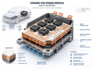
  • Power semiconductor substrates
  • EV power electronics
  • Industrial motor control modules
  • RF power amplifiers
  • Medical power devices
  • Aerospace and defense electronic modules
  • Compact DC-DC converters
  • High-voltage sensor and insulation circuits

Ceramic also performs well in applications where high voltage and heat appear together. Many ceramic substrates provide high dielectric strength, low moisture absorption, and stable insulation performance. These features are valuable for power modules that must operate safely and consistently over time.

FR4 remains widely used in power electronics as well. Many power supplies, inverters, chargers, and control boards use FR4 successfully. The key is that FR4 often needs additional thermal design support. This may include heavier copper, thermal vias, heat sinks, insulated metal substrates, or mechanical heat spreaders.

A useful way to decide is to review the heat path. If the main heat path depends on the PCB base material, ceramic is worth serious consideration. If the heat can be handled by copper, airflow, housing, or external heat sinks, FR4 may keep the project more cost-efficient.
Ceramic PCB vs FR4: Which PCB Material Should You Choose?

When Should You Choose an FR4 PCB?

You should choose an FR4 PCB when your project needs a proven, economical, and flexible board material for general electronic functions. FR4 is especially suitable for signal routing, digital circuits, control boards, moderate-power applications, and products where cost control matters.

FR4 is a strong choice when your design has these characteristics:

  • The circuit is mainly digital, analog, control, or mixed-signal.
  • Heat generation is moderate and manageable through layout.
  • The project needs multilayer routing.
  • The budget requires efficient material cost.
  • The board needs common PCB processes such as plated through holes, impedance control, solder mask, and standard surface finish.
  • The product does not require extreme thermal conductivity from the substrate.
  • The design needs quick prototyping and easy scaling to production.

Here is a simple guide:

Project RequirementIs FR4 a Good Choice?Reason
Low to medium heatYesThermal needs can usually be handled by layout and copper design
Complex multilayer routingYesFR4 multilayer fabrication is highly mature
Cost-sensitive productionYesMaterial and processing costs are efficient
General control electronicsYesFR4 supports stable, reliable circuit performance
Very high heat densityDependsAdditional thermal structures may be needed
High-power LED chip directly on boardSometimes, but ceramic or metal core may perform betterHeat path becomes more critical
RF or microwave circuitDependsSpecial RF laminates or ceramic may be needed for tighter performance

When customers contact EBest Circuit for a new PCB project, FR4 is often the first material we evaluate because it is practical and widely suitable. If the design review shows that FR4 can meet the electrical, thermal, and mechanical requirements, it often provides the best cost-performance ratio.

When Should You Choose a Ceramic PCB?

You should choose a ceramic PCB when your design needs high thermal conductivity, strong insulation, compact heat management, high-frequency stability, or long-term reliability in demanding environments. Ceramic is especially valuable when performance stability matters more than material cost.

Ceramic PCB is a strong choice when the project has these needs:

  • High heat generation from LEDs, power chips, laser diodes, or RF devices
  • Compact board size with limited heat-spreading area
  • Strong electrical insulation under high voltage
  • Stable dielectric properties for high-frequency circuits
  • High reliability under thermal cycling
  • Low moisture absorption for sensitive applications
  • Good dimensional stability for precision assembly
  • Longer service life in industrial, medical, automotive, or aerospace products

The type of ceramic also matters. Alumina is popular because it balances performance and cost. Aluminum nitride is preferred when thermal conductivity is the main priority. Silicon nitride can support applications that need strong mechanical reliability and thermal performance. The circuit process also matters because DPC, DBC, AMB, thick film, and thin film ceramic boards serve different design goals.

A practical selection table can help:

Application NeedSuitable Ceramic OptionWhy It Helps
Balanced thermal performance and costAlumina ceramic PCBReliable, widely used, stable, and cost-effective among ceramics
Very high thermal conductivityAluminum nitride ceramic PCBExcellent heat transfer for dense power designs
High-current power moduleDBC or AMB ceramic substrateStrong copper bonding and power handling
Fine lines and precision circuitsDPC or thin-film ceramic PCBSupports accurate circuit features
Harsh working environmentAlumina, AlN, or Si3N4 depending on designStable insulation and thermal performance

EBest Circuit (Best Technology) supports ceramic PCB material selection, DFM review, prototype production, and PCBA assembly support.

Ceramic vs PCB: Is Ceramic a PCB Material or a PCB Type?

Ceramic is a PCB material, and a ceramic PCB is a PCB type that uses ceramic as its substrate. Because PCB refers to the finished printed circuit board, while ceramic refers to the base material used to build a certain kind of PCB.

Think of PCB as the general product category. Inside that category, there are many material and structure options. FR4 PCB, ceramic PCB, aluminum PCB, copper core PCB, rigid-flex PCB, and high-frequency PCB are all different forms of printed circuit boards.

Here is a simple explanation:

TermMeaningExample
PCBPrinted circuit board used to connect and support componentsAny electronic circuit board
FR4 PCBPCB made with FR4 glass epoxy laminateControl board, IoT board, industrial PCB
Ceramic PCBPCB made with ceramic substrateLED module, power substrate, RF module
Ceramic materialThe substrate material used in ceramic PCBAlumina, aluminum nitride, silicon nitride
PCB typeA board category based on structure or materialFR4, ceramic, metal core, rigid-flex

This distinction matters because the design process still follows PCB principles. Engineers still need Gerber files, copper layers, pads, spacing, surface finish, soldering requirements, and testing plans. The difference is that ceramic substrates require specific manufacturing methods and design rules. Hole processing, edge treatment, copper bonding, and metallization are different from standard FR4 fabrication.

Which PCB Material Is Better for LED, Power, and RF Applications?

The better PCB material depends on the application. For standard LED driver boards, FR4 may be suitable. For high-power LED modules where heat must move quickly from the light source, ceramic PCB or metal core PCB is often stronger. For power electronics, FR4 works well in control sections, while ceramic is preferred for dense power substrates. For RF circuits, material choice depends on frequency, dielectric stability, loss, and thermal needs.

For LED applications, ceramic PCB is attractive when the LED package produces high heat in a small area. Ceramic helps move heat away from the LED, which can support stable brightness and longer product life. FR4 can still be used in LED driver circuits, control boards, and lower-power lighting products.

For power applications, ceramic PCB performs well when the substrate must provide both insulation and heat transfer. This is common in power modules, high-voltage circuits, and compact converters. FR4 is still widely used for power supply control boards, gate driver boards, and general power electronics where the thermal design can be handled with copper, vias, and external heat sinks.

For RF applications, ceramic can provide stable dielectric properties and good thermal behavior, especially in compact or high-power RF modules. However, many RF PCBs also use specialized laminates such as Rogers materials, PTFE-based materials, or hydrocarbon ceramic-filled laminates.

ApplicationFR4 PCBCeramic PCBPractical Recommendation
Low-power LED control boardVery suitableUsually more than neededFR4 is often practical
High-power LED modulePossible with careful thermal designVery suitableCeramic or metal core PCB is often preferred
LED driver circuitVery suitableSelected for special thermal or insulation needsFR4 is common
Power control boardVery suitableUsed when heat or insulation requirements are highChoose based on heat density
Power module substrateLimited in high heat density modulesExcellentCeramic is often stronger
RF low-frequency circuitSuitable in many casesSometimes selectedFR4 may work if requirements are moderate
RF high-power or high-stability circuitDepends on frequency and loss limitsStrong optionCeramic or RF laminate may be better
Medical or aerospace high-reliability electronicsSuitable for many control circuitsStrong for thermal and stable substrate needsReview reliability target carefully

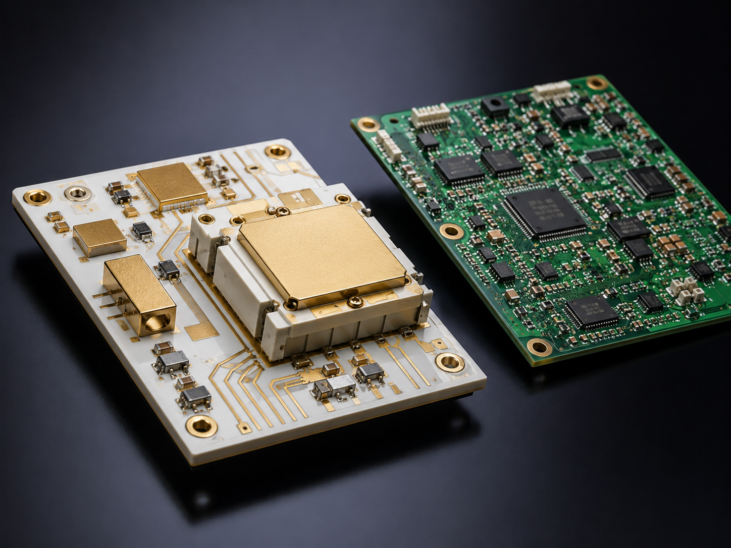
The strongest material choice is usually application-specific. A product can also use more than one PCB type. For example, a power device may use an FR4 control board and a ceramic power substrate in the same assembly. EBest Circuit supports PCB fabrication and PCBA assembly for different material categories, including FR4, metal core PCB, ceramic PCB, RF PCB, and high-reliability boards.
Ceramic PCB vs FR4: Which PCB Material Should You Choose?

Why Is Ceramic PCB More Expensive Than FR4 PCB?

Ceramic PCB is more expensive than FR4 PCB because the raw material, manufacturing process, metallization method, processing difficulty, and inspection requirements are more demanding. Ceramic substrates are harder and more brittle than FR4 laminates, so cutting, drilling, edge processing, copper bonding, and surface preparation require specialized control.

FR4 manufacturing is extremely mature and widely scaled. Material supply is broad, production lines are optimized, and standard processes can produce large volumes efficiently. Ceramic PCB production is more specialized. The factory must control substrate quality, metallization adhesion, copper thickness, dimensional tolerance, and thermal reliability with greater precision.

The cost difference comes from several main factors:

Cost FactorCeramic PCBFR4 PCB
Raw materialHigher-cost ceramic substratesCost-efficient laminate materials
Processing methodSpecialized laser, mechanical, metallization, or bonding processesMature drilling, plating, imaging, etching, and lamination
Copper bondingRequires ceramic-compatible metallization or direct bondingStandard copper-clad laminate process
Tooling and handlingMore careful handling due to hardness and brittlenessMore forgiving in standard fabrication
Yield controlRequires tight control for cracks, adhesion, and flatnessHighly standardized yield management
Application requirementsOften used in high-reliability productsUsed across broad commercial and industrial products
Production scaleMore specialized volumesLarge global production scale

Ceramic PCB cost also depends on material type. Alumina is usually more economical than aluminum nitride. Aluminum nitride offers much higher thermal conductivity, so it carries a higher material cost. The circuit process also changes pricing. DPC, DBC, AMB, thick film, and thin film processes have different cost structures.

Board size, copper thickness, line width, spacing, hole design, surface finish, tolerance, and inspection level also affect price. A simple alumina ceramic PCB may be relatively manageable in cost. A high-power AMB substrate or fine-line DPC ceramic board may require a higher budget because it delivers more advanced performance.

EBest Circuit (Best Technology) can support material selection, DFM review, PCB fabrication, component sourcing, PCBA assembly, and testing for projects moving from prototype to production. For engineers comparing FR4 vs ceramic, our team can review your Gerber files, stackup, power conditions, and reliability targets before recommending the most suitable board solution.

For project review or quotation support, contact EBest Circuit (Best Technology) at sales@bestpcbs.com.
You may also like

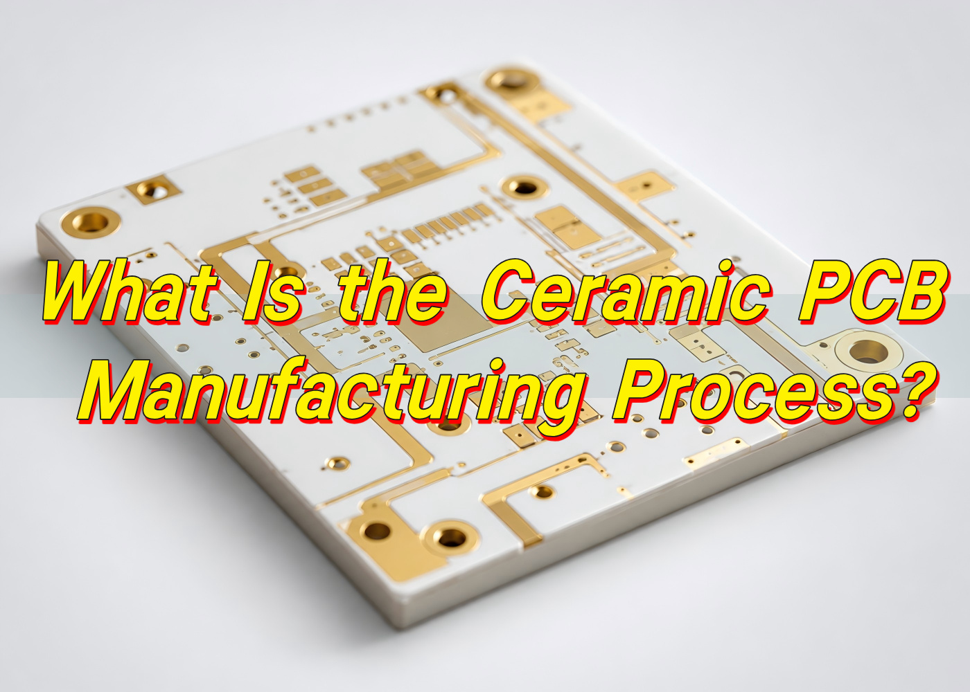
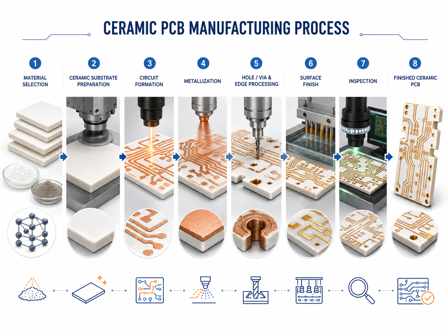
What Is the Ceramic PCB Manufacturing Process?

May 13th, 2026

What Is the Ceramic PCB Manufacturing Process?

The ceramic PCB manufacturing process is the sequence of material preparation, substrate processing, circuit formation, metallization, finishing, inspection, and packaging used to produce ceramic-based printed circuit boards. Unlike standard FR4 boards, ceramic PCBs use inorganic ceramic substrates such as alumina, aluminum nitride, silicon nitride, or zirconia-toughened alumina.

The ceramic board itself is not only a carrier for copper circuits; it is also part of the thermal management structure. That is why the production route must be carefully controlled from raw ceramic substrate selection to final surface finish.

What Is the Ceramic PCB Manufacturing Process?

A typical ceramic PCB project may involve DPC, DBC, AMB, thick film, LTCC, or HTCC technology. Each process has its own material rules, conductor system, copper thickness range, and design restrictions. For example, DPC is often selected for fine circuits and high-density layouts, while DBC and AMB are widely used for higher-power applications that require thicker copper and stronger thermal paths.

EBest Circuit (Best Technology) supports ceramic PCB manufacturing and ceramic PCB assembly, with process capabilities covering materials such as Al2O3, AlN, ZTA, and Si3N4, as well as DPC, DBC, AMB, thick film, LTCC, and HTCC technologies. The company information also lists quality certifications including IATF 16949, ISO 9001:2015, ISO 13485:2016, AS9100D, REACH, RoHS, and UL.

What Ceramic PCB Materials Are Commonly Used?

Ceramic PCB materials are selected according to thermal conductivity, dielectric performance, mechanical strength, coefficient of thermal expansion, cost target, and end-use environment.

The most widely used ceramic PCB materials include alumina, aluminum nitride, silicon nitride, and zirconia-toughened alumina. Each material has a different engineering personality. Alumina is cost-effective and widely available. Aluminum nitride offers much higher thermal conductivity. Silicon nitride is valued for strength and thermal shock resistance. ZTA provides improved toughness compared with standard alumina.

Ceramic PCB MaterialMain StrengthTypical Use CasePractical Selection Note
Alumina PCB, Al2O3Good insulation, stable performance, balanced costLED modules, sensors, power electronics, general ceramic circuitsA common starting point for ceramic PCB prototype and volume production
Aluminum Nitride PCB, AlNHigh thermal conductivity, low thermal expansionHigh-power LED, laser diode, RF power, power semiconductor modulesChosen when heat dissipation is a leading design requirement
Silicon Nitride PCB, Si3N4High mechanical strength, thermal shock resistanceAutomotive power modules, harsh-environment electronicsSuitable for applications with mechanical and thermal stress
ZTA Ceramic PCBBetter toughness than pure aluminaIndustrial electronics, power control, demanding substratesUseful when designers need stronger mechanical durability
LTCC CeramicMultilayer ceramic structure, embedded conductorsRF modules, filters, compact electronic packagesSuitable for compact multilayer ceramic circuits
HTCC CeramicHigh-temperature co-fired ceramic structureAerospace, high-temperature sensors, hermetic packagesOften selected for high-temperature and high-reliability environments

Alumina is often the first choice when the design needs ceramic benefits at a reasonable cost. It offers good dielectric strength, chemical resistance, and mechanical stability. For many industrial and LED applications, alumina gives a practical balance between performance and budget.

Aluminum nitride is selected when thermal performance becomes more important. It transfers heat far more efficiently than alumina, which makes it attractive for high-power chips, laser components, high-brightness LED modules, and compact power devices. Its coefficient of thermal expansion is also closer to silicon, which can support better reliability in semiconductor-related designs.

Silicon nitride and ZTA are used when strength and fracture resistance become part of the design conversation. These materials are helpful in applications exposed to vibration, thermal cycling, or mechanical pressure. Although they may carry a higher cost, they provide valuable stability in demanding environments.

How Does the Ceramic Manufacturing Process Start?

For ceramic PCBs, the early stage usually includes engineering review and process selection. The supplier checks whether the design is better suited for DPC, DBC, AMB, thick film, LTCC, or HTCC. This decision has a direct influence on copper thickness, minimum line width, hole processing, surface finish, cost, and delivery time.

The beginning stage often includes:

  • Reviewing Gerber files, drill files, drawings, stack-up, and copper thickness requirements.
  • Confirming ceramic substrate type, such as alumina, AlN, Si3N4, or ZTA.
  • Checking whether the circuit needs fine traces, thick copper, high-voltage spacing, or strong thermal transfer.
  • Evaluating hole size, edge tolerance, board thickness, and panelization method.
  • Confirming the surface finish for soldering, wire bonding, or long-term storage.

This early review is highly valuable for ceramic PCB prototype projects. Many prototypes are built for electrical testing, thermal testing, or mechanical validation. The ceramic production process also begins with substrate procurement or in-house substrate preparation. For standard alumina or aluminum nitride thicknesses, manufacturers may use pre-sintered ceramic sheets.

What Is the Ceramic PCB Manufacturing Process?

How Are Ceramic Substrates Prepared?

Ceramic substrate preparation creates the foundation for the entire board. A stable substrate supports accurate circuit formation, reliable metallization, clean edge processing, and strong assembly results. Any issue in flatness, thickness, surface quality, or internal structure can influence later steps.

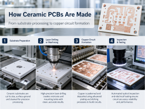
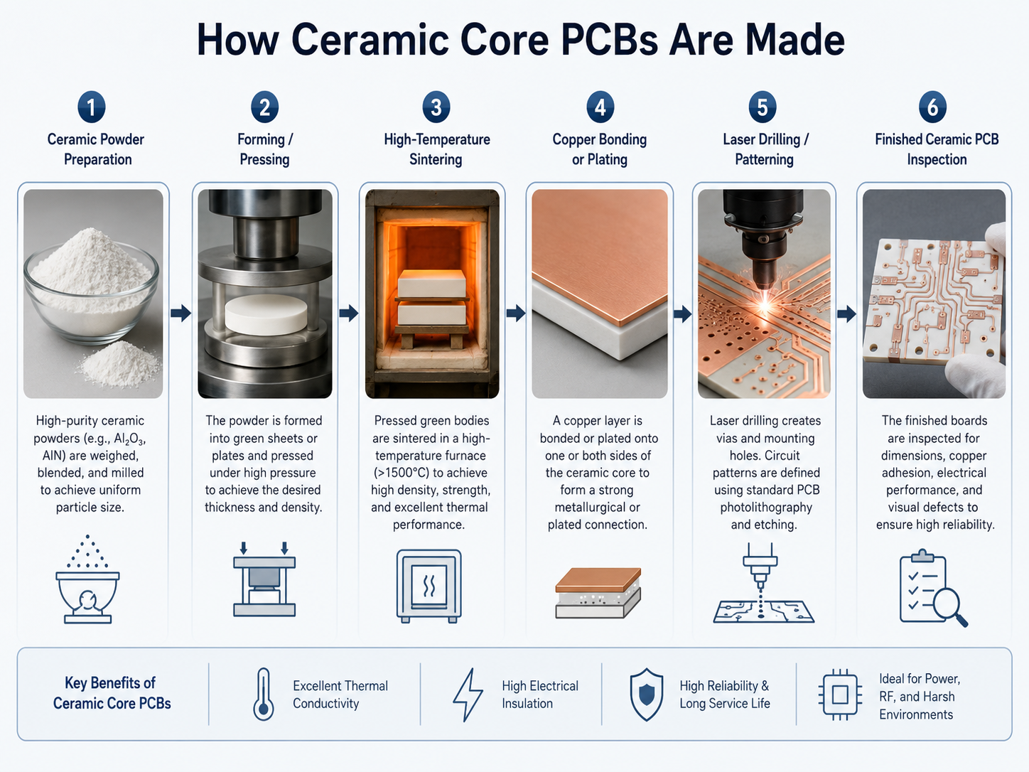
In a traditional ceramic production process, ceramic powder is mixed with binders, solvents, plasticizers, and other additives. The mixture is shaped by tape casting, dry pressing, extrusion, or injection molding, depending on the substrate type and final application. After forming, the green ceramic body is dried and sintered at high temperature. During sintering, organic materials burn out and ceramic particles bond together into a dense, hard substrate.

For ceramic PCB manufacturing, many projects start from fired ceramic substrates. These sheets are inspected for thickness, surface condition, warpage, cracks, chips, and contamination. The substrate may then be cleaned, lapped, polished, laser-cut, drilled, or prepared for metallization.

Typical ceramic substrate preparation steps include cleaning, dimensional inspection, surface activation, laser drilling, contour pre-processing, and panel arrangement. Cleanliness is especially important because ceramic surfaces must bond well with copper, tungsten, silver, gold, or other metallization systems. Dust, oil, or weak surface energy can affect adhesion and long-term stability.

EBest Circuit’s ceramic PCB capability information includes common substrate thicknesses such as 0.38 mm, 0.635 mm, and 1.0 mm for Al2O3 and AlN, as well as 0.25 mm and 0.32 mm for Si3N4.

How Are Circuits Formed on Ceramic PCBs?

Circuit formation on ceramic PCBs depends on the selected manufacturing technology. The circuit can be built through direct copper plating, bonded copper foil, active metal brazing, thick film printing, or co-fired ceramic processing. Each route produces a different structure and supports different applications.

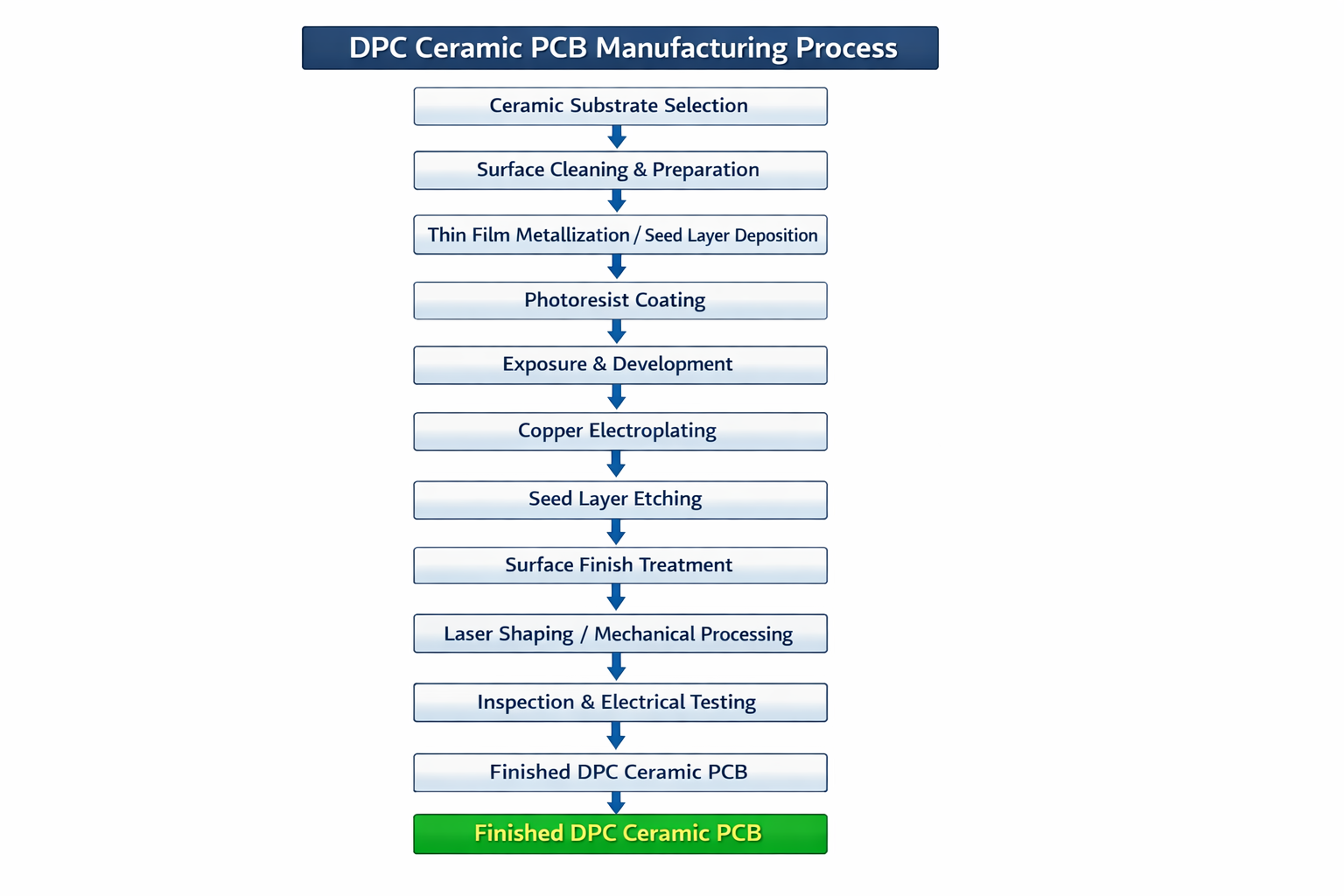
In DPC, or Direct Plated Copper, the ceramic surface is usually activated and plated with copper. This method supports fine circuits, good dimensional accuracy, and relatively thin copper layers compared with DBC or AMB. DPC is often chosen for LED substrates, sensors, optoelectronics, and ceramic PCB prototype work where precision is important.

In DBC, or Direct Bonded Copper, copper foil is bonded directly to the ceramic substrate through a high-temperature bonding process. DBC ceramic PCBs can carry higher current and dissipate heat well, which makes them popular in power electronics, IGBT modules, automotive power systems, and high-power LED modules.

AMB, or Active Metal Brazing, uses active brazing materials to bond copper to ceramic. It is often used with silicon nitride ceramic because the bond strength and mechanical reliability are well suited for demanding power modules. AMB substrates can provide excellent thermal cycling performance and strong copper adhesion.

Thick film ceramic PCBs use screen printing to apply conductive paste onto the ceramic substrate. The printed circuit is then dried and fired. Conductive materials may include silver, palladium silver, gold, or other paste systems. Thick film technology is useful for hybrid circuits, sensors, heaters, resistive networks, and certain compact electronic modules.

LTCC and HTCC use co-fired ceramic technology. Conductive patterns are formed on ceramic green tapes, then stacked, laminated, and fired together. LTCC is often used for RF modules and compact multilayer circuits. HTCC is used for high-temperature and high-reliability packages.

Circuit Formation MethodBrief DescriptionSuitable ApplicationsMain Advantage
DPCCopper is plated onto ceramic after surface activationFine circuits, LED, sensors, prototypesGood precision and clean circuit definition
DBCCopper foil is bonded directly to ceramicPower modules, high-current boardsThick copper and strong heat transfer
AMBCopper is brazed to ceramic with active metalAutomotive power, Si3N4 substratesStrong bonding and thermal cycling reliability
Thick FilmConductive paste is printed and firedHybrid circuits, sensors, heatersFlexible patterning and mature process
LTCCCeramic tapes and conductors are co-firedRF modules, compact multilayer designsMultilayer integration
HTCCHigh-temperature co-fired ceramic structureHermetic packages, aerospace, sensorsHigh-temperature endurance
What Is the Ceramic PCB Manufacturing Process?

What Is the Role of Metallization in Ceramic PCB Manufacturing?

Metallization is one of the most important steps in ceramic PCB manufacturing because ceramic itself is insulating. To create electrical circuits, solderable pads, vias, and bonding areas, the ceramic surface must receive a conductive metal layer. This metal layer must bond firmly to the ceramic and remain stable during thermal cycling, soldering, and long-term operation.

The metallization system depends on the process type. DPC commonly uses sputtering or seed-layer deposition followed by copper electroplating. Thick film ceramic PCBs use fired metal pastes. LTCC and HTCC may use tungsten, molybdenum, silver, gold, or other conductor systems that can withstand the firing environment. DBC and AMB rely on copper bonding technology to create strong metal-ceramic adhesion.

In real production, metallization is controlled through surface preparation, metal thickness, adhesion testing, pattern accuracy, and inspection. For high-power boards, copper thickness becomes especially important. EBest Circuit’s ceramic PCB process information lists outer copper capability for DPC and thicker copper ranges for DBC and AMB, which reflects the different roles these processes play in precision circuits and power substrates.

Metallization also affects assembly choices. If the customer plans to use soldering, ENIG, immersion silver, immersion tin, or other solderable finishes may be selected. If the customer plans to use wire bonding, gold-related finishes may be more suitable. If the board will operate in a high-temperature or high-current environment, the metallization structure must be reviewed carefully during DFM.

How Are Holes, Vias, and Edges Processed?

Holes, vias, and edges are processed through laser machining, mechanical drilling, grinding, routing, dicing, or precision cutting. Ceramic is harder and more brittle than FR4, so these operations require controlled tooling and stable process parameters.

For ceramic PCBs, holes may be plated through holes, non-plated holes, laser vias, mounting holes, or thermal vias. The hole design depends on the circuit requirement and mechanical assembly method. Small holes are often made by laser drilling because ceramic material is difficult to machine with standard PCB drilling tools. Larger holes and edges may use CNC grinding, laser cutting, waterjet cutting, or diamond tooling.

Edge processing is also important. Ceramic boards often have tight outline tolerances, especially when used in power modules, LED packages, sensors, or custom housings. Chips, microcracks, and rough edges should be controlled because they may influence mechanical strength and assembly fit.

Typical hole and edge processing considerations include:

  • Minimum plated and non-plated hole size.
  • Hole tolerance and position accuracy.
  • Aspect ratio for plated holes.
  • Distance from circuit to board edge.
  • Outline tolerance for custom shapes.
  • Edge smoothness and chipping control.
  • Panel format for production and assembly.

What Surface Finishes Are Used for Ceramic PCBs?

Surface finish protects exposed metal and supports soldering, wire bonding, storage, and assembly. Since ceramic PCBs are often used in high-reliability applications, the finish should match the component type, assembly method, bonding process, and operating environment.

What Is the Ceramic PCB Manufacturing Process?

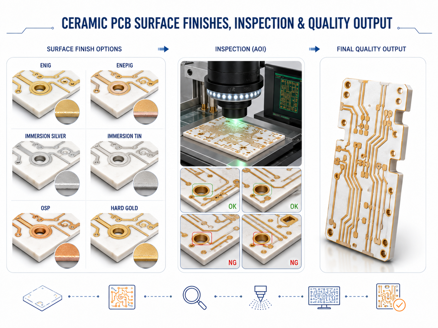
Common ceramic PCB surface finishes include ENIG, ENEPIG, immersion silver, immersion tin, OSP, hard gold, and sometimes special gold systems for wire bonding. The best option depends on whether the customer needs solderability, aluminum wire bonding, gold wire bonding, high wear resistance, or stable shelf life.

Surface FinishBrief DescriptionSuitable UsePractical Note
ENIGNickel layer with thin immersion goldSMT assembly, general soldering, stable storagePopular and versatile for many ceramic PCB assemblies
ENEPIGNickel, palladium, and gold finishWire bonding and solderingGood for advanced packaging and mixed assembly needs
Immersion SilverThin silver finish over copperHigh-speed signals, solderingGood conductivity and solderability with proper storage
Immersion TinTin finish over copperSoldering applicationsCost-friendly for selected designs
OSPOrganic protective coatingShorter storage cycles and solderingSimple finish for certain copper surfaces
Hard GoldElectroplated nickel-gold finishWear areas, contacts, selected bonding padsUseful where contact durability is important

ENIG is often chosen because it gives good solderability and a flat pad surface. It is suitable for many ceramic PCB assembly projects. ENEPIG is selected when the board requires both soldering and wire bonding, especially in more advanced electronic packages. Hard gold may be used where repeated contact or wear resistance is required.

Surface finish thickness should be controlled. For example, nickel and gold thickness have a direct effect on soldering behavior and bondability. According to the supplied EBest Circuit capability data, available finishes include OSP, ENIG, immersion silver, immersion tin, ENEPIG, and hard gold, with listed thickness ranges for each finish.

What Factors Affect Ceramic PCB Cost?

Ceramic PCB cost is affected by material type, substrate thickness, copper thickness, process route, circuit density, hole structure, tolerance, surface finish, quantity, and assembly requirements.

The biggest cost factor is often the ceramic material itself. Alumina is usually more economical, while aluminum nitride and silicon nitride are more expensive because they offer stronger thermal or mechanical performance. The second major factor is the manufacturing process. DPC, DBC, AMB, thick film, LTCC, and HTCC do not share the same cost structure.

Copper thickness also matters. Thin copper for fine circuits is different from thick copper for power modules. DBC and AMB substrates with heavy copper require more material and tighter process control. Small holes, tight tolerances, complex outlines, and special surface finishes also increase production effort.

Cost FactorWhy It MattersCost Impact
Ceramic materialAl2O3, AlN, Si3N4, and ZTA have different raw material costsHigh
Manufacturing processDPC, DBC, AMB, thick film, LTCC, and HTCC use different equipment and stepsHigh
Copper thicknessThicker copper supports current and heat but needs more processing controlMedium to High
Board size and panel useLarger or irregular boards may reduce panel efficiencyMedium
Hole and via designSmall holes, dense vias, and tight tolerances increase machining timeMedium
Surface finishENEPIG and hard gold cost more than simpler finishesMedium
QuantityPrototype orders carry more setup cost per pieceMedium
Testing and inspectionHigh-reliability applications may require more documentation and checksMedium

A good way to manage cost is to align the design with the real performance target. For example, if alumina meets the thermal requirement, there may be no need to choose aluminum nitride. If DPC provides enough copper thickness and line accuracy, DBC may not be necessary. If ENIG is enough for soldering, ENEPIG may only be needed when wire bonding is required. This kind of DFM thinking helps customers receive a board that performs well without unnecessary specification inflation.

FAQs About Ceramic PCB Manufacturing Process

ItemCeramic Manufacturing ProcessCeramic PCB Manufacturing Process
Main GoalMake ceramic material or ceramic partsMake an electronic circuit board on ceramic
Key StepsForming, drying, sintering, polishingSubstrate prep, metallization, circuit formation, finish, testing
OutputCeramic plate, block, tube, or partCeramic printed circuit board
Main FocusMaterial density, shape, strengthElectrical path, heat transfer, solderability, reliability
Typical UsersCeramic parts buyers, industrial part makersElectronics engineers, EMS companies, power module designers
  • 2. What is the difference between alumina and aluminum nitride ceramic PCB materials?

Alumina and aluminum nitride are both popular ceramic PCB materials, but they serve different performance levels. Alumina is widely used because it is stable, insulating, cost-effective, and available in many specifications. It is a strong choice for general ceramic PCBs, LED boards, sensors, and industrial circuits.

Aluminum nitride has much higher thermal conductivity. It is selected when heat must move away from chips or power devices quickly. This makes AlN a strong fit for high-power LED modules, laser diodes, RF power devices, semiconductor packaging, and compact power electronics.

  • 3. Can ceramic PCB prototypes be made in small quantities?

Yes, ceramic PCB prototypes can be made in small quantities. Prototype production is common for thermal testing, electrical validation, LED module evaluation, power device testing, and new product development.

  • 4. Are ceramic PCBs suitable for high-power electronics?

Yes, ceramic PCBs are highly suitable for high-power electronics. Their strong thermal conductivity, high insulation strength, and dimensional stability make them a preferred choice for power modules, LED lighting, automotive power systems, RF power devices, laser modules, and energy-related electronics.

  • 5. What files does a ceramic PCB manufacturer need?

A ceramic PCB manufacturer usually needs complete production files and clear technical requirements. The more complete the documentation is, the smoother the review and quotation process will be.

Commonly requested files include:

  • Gerber files for circuit layers, solder mask, silkscreen, and paste layers.
  • Drill files for plated and non-plated holes.
  • Mechanical drawing with board outline, thickness, tolerance, and special notes.
  • Stack-up or substrate requirement, including ceramic material and thickness.
  • Copper thickness requirement and surface finish selection.
  • BOM and assembly drawing if ceramic PCB assembly is required.
  • Special test requirements, such as electrical test, thermal inspection, or visual criteria.
  • 6. How long does ceramic PCB production usually take?

Ceramic PCB production time depends on material availability, process type, quantity, complexity, surface finish, and whether assembly is included. A simple alumina DPC prototype may move faster than a customized AMB or LTCC project. Boards with special thickness, tight tolerances, heavy copper, or advanced finishes usually need more production planning.

  • 7. Why are ceramic PCBs more expensive than FR4 PCBs?

Ceramic PCBs are more expensive than FR4 PCBs because the materials, equipment, and process controls are more specialized. FR4 is easy to laminate, drill, route, and process in large volumes. Ceramic substrates are harder, more brittle, and more demanding during drilling, cutting, metallization, and finishing.

In brief, the ceramic PCB manufacturing process turns a high-performance ceramic substrate into a reliable electronic interconnect through careful material selection, substrate preparation, circuit formation, metallization, machining, finishing, and inspection. For engineers working on power, LED, RF, medical, automotive, or industrial electronics, choosing the right ceramic PCB materials and an experienced ceramic PCB manufacturer can make product development smoother and more predictable. For ceramic PCB manufacturing, ceramic PCB prototype, or ceramic PCB assembly support, you can contact sales@bestpcbs.com

You may also like

Ceramic PCB Manufacturer USA Serving | Alumina & AlN Boards

May 12th, 2026

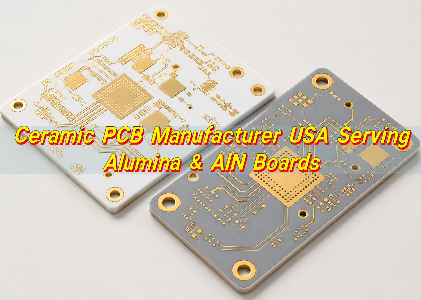
What is a ceramic PCB manufacturer serving USA?

For many buyers, the phrase ceramic pcb manufacturer usa does not only mean “a factory physically located in the USA.” It often means a capable ceramic PCB supplier that can serve U.S. projects with dependable engineering support, export experience, and quality systems suitable for demanding applications.

Ceramic PCB Manufacturer USA Serving | Alumina & AlN Boards

Ceramic PCBs are different from standard FR4 boards because the base material is a ceramic substrate, such as alumina or aluminum nitride. These materials offer excellent thermal conductivity, electrical insulation, dimensional stability, and high-temperature endurance. That is why ceramic PCB technology is widely used in power electronics, LED modules, medical devices, aerospace electronics, RF modules, automotive electronics, sensors, and other products where heat, reliability, and compact design matter.

When a U.S. customer searches for a ceramic PCB partner, the real question is usually simple: can this supplier manufacture the correct ceramic substrate, control the process, support the design review, and deliver boards that perform as expected?

EBest Circuit(Best Technology), serves U.S. customers with ceramic PCB fabrication and assembly support for prototype, low-volume, medium-volume, and production requirements. The company provides custom ceramic PCB manufacturing, turnkey PCB and PCBA services, and multiple ceramic processes, including DPC, DBC, AMB, thick film, LTCC, and HTCC. Its ceramic PCB capabilities include alumina, aluminum nitride, ZTA, silicon nitride, several conductor options, multiple surface finishes, and certified quality systems including ISO 9001, ISO 13485, IATF 16949, AS9100D, RoHS, REACH, and UL recognition.

What materials do ceramic PCB manufacturers for USA offer?

Ceramic PCB manufacturers serving USA customers usually offer several substrate materials. The most common ceramic PCB materials are alumina and aluminum nitride, but advanced projects may also require silicon nitride, zirconia-toughened alumina, LTCC materials, or HTCC materials.

Alumina ceramic PCB is one of the most widely used choices because it provides a balanced mix of insulation, thermal performance, mechanical durability, and cost control. It is commonly used in LED lighting, power modules, sensors, hybrid circuits, and industrial electronics. Alumina is available in different purity levels, such as 92% and 96%, and some manufacturers can support special variants such as black alumina.

Aluminum nitride, often written as AlN, is selected when thermal performance is a main priority. Compared with alumina, AlN has much higher thermal conductivity and a thermal expansion behavior that works well with certain semiconductor and power device packages. This makes it a strong choice for high-power LED modules, laser diodes, power conversion modules, RF power devices, aerospace electronics, medical imaging electronics, and other compact systems that generate concentrated heat.

Some advanced projects also use silicon nitride, ZTA, LTCC, or HTCC. Silicon nitride offers high strength, high toughness, good thermal conductivity, and excellent thermal shock resistance. ZTA combines alumina with zirconia to improve toughness and mechanical reliability. LTCC and HTCC are often used for multilayer ceramic circuits, high-frequency modules, sensors, and compact electronic packages.

Ceramic PCB MaterialMain StrengthTypical Use CasesCommon Reason to Choose It
Alumina PCBGood insulation, stable performance, cost-effective ceramic baseLED modules, sensors, power circuits, industrial electronicsBalanced ceramic performance and practical cost
Aluminum Nitride PCBHigh thermal conductivity and good CTE behaviorPower electronics, RF power modules, laser modules, medical electronicsBetter heat dissipation in compact designs
Silicon Nitride PCBHigh mechanical strength and thermal shock resistanceAutomotive power modules, harsh environments, high-reliability electronicsStronger mechanical reliability
ZTA PCBImproved toughness compared with standard aluminaIndustrial and power applicationsBetter crack resistance and durability
LTCCMultilayer ceramic structure, good for compact circuitsRF modules, sensors, microwave devices, integrated packagesCompact multilayer ceramic integration
HTCCHigh-temperature ceramic circuit capabilityAerospace, defense-related commercial electronics, harsh applicationsHigh-temperature endurance and stable insulation

For most U.S. projects, the best starting point is to match the material to the real design challenge. If the main issue is controlled heat transfer at a reasonable cost, alumina may be suitable. If the design has a very hot component, tight thermal limits, or high power density, aluminum nitride may be the better direction. If the board needs extra toughness, silicon nitride or ZTA may deserve attention. If the product requires ceramic multilayer routing, LTCC or HTCC may be a stronger path than a simple single-sided or double-sided ceramic board.

EBest Circuit supports several ceramic PCB materials and process types, which gives U.S. customers more flexibility during design evaluation. Instead of forcing one standard material into every project, the engineering team can review thermal requirements, copper thickness, operating temperature, board size, assembly needs, and budget targets.

Can China ceramic PCB suppliers meet USA aerospace/medical standards?

China ceramic PCB suppliers can meet the expectations of USA aerospace and medical customers when they have the right manufacturing capability, quality certifications, process controls, and documentation discipline. The key is not the country alone. The key is whether the supplier can build to controlled requirements, maintain traceability, support audits, and provide reliable production records.

For advanced ceramic PCB projects, U.S. customers should evaluate the supplier’s quality system, engineering response, material control, inspection process, and shipment reliability before placing important orders.

Aerospace and medical electronics often require more than basic PCB fabrication. These markets value documented processes, controlled materials, repeatable production, inspection evidence, and clear communication. Aerospace customers may look for AS9100D alignment, first article inspection support, lot traceability, controlled process records, and stable supplier management. Medical customers may look for ISO 13485, process documentation, component traceability for assembly projects, clean handling practices, and long-term quality consistency.

EBest Circuit’s positioning is especially relevant here because the company supports ceramic PCB fabrication and ceramic PCB assembly under a quality framework that includes ISO 9001, ISO 13485, IATF 16949, AS9100D, RoHS, REACH, and UL. For U.S. medical, aerospace, automotive, and industrial customers, these certifications help show that the supplier has invested in quality management and controlled production practices.

For ceramic PCB projects going into regulated or high-reliability products, the manufacturer should provide practical support in several areas:

  • Material selection records, substrate specifications, and copper or conductor details.
  • Engineering review for manufacturability, tolerances, hole sizes, surface finish, and thermal design.
  • Inspection methods such as visual inspection, dimensional checks, electrical testing, and process-specific validation.
  • Production traceability by order, lot, material batch, and process route.
  • Clear export packaging, shipping documentation, and communication for USA delivery.

The best approach is to treat the supplier qualification step as part of the design process. U.S. customers can request the manufacturer’s certifications, capability table, sample reports, material options, and previous industry experience. They can also start with a prototype order, review the board quality, check communication speed, and then move toward repeat orders or volume production.

Ceramic PCB Manufacturer USA Serving | Alumina & AlN Boards

What certifications should a USA-serving ceramic PCB manufacturer have?

A USA-serving ceramic PCB manufacturer should have certifications that match the application risk level and target industry. For general industrial electronics, ISO 9001 is usually the baseline. For medical device electronics, ISO 13485 is highly valuable because it focuses on quality management for medical device-related manufacturing. For automotive electronics, IATF 16949 is an important signal of process control and automotive supply chain discipline. For aerospace electronics, AS9100D is especially relevant because it aligns with aerospace quality management expectations. RoHS and REACH are also important for material compliance, especially when products are sold into global markets.

Certification or Compliance ItemWhy It Matters for USA CustomersTypical Application Relevance
ISO 9001Shows a structured quality management systemGeneral PCB and PCBA manufacturing
ISO 13485Supports medical device quality expectationsMedical electronics, monitoring devices, diagnostic equipment
IATF 16949Supports automotive process disciplineAutomotive electronics, EV systems, lighting, control modules
AS9100DSupports aerospace quality management expectationsAerospace electronics, UAV electronics, avionics-related commercial projects
ULSupports recognized material or product safety-related requirementsProducts requiring UL-recognized manufacturing inputs
RoHSRestricts hazardous substances in electronicsGlobal electronics, consumer, industrial, medical, automotive
REACHSupports chemical compliance for global marketsElectronics exported to compliance-sensitive regions

A ceramic PCB manufacturer serving USA customers should also understand that certifications are not only marketing badges. They should influence how the supplier handles document control, incoming inspection, production routing, staff training, nonconforming material, corrective actions, equipment maintenance, and final inspection. This matters because ceramic PCB production can involve special processes such as metallization, firing, plating, laser drilling, DPC, DBC, AMB, or thick film printing. Each process needs stable control to produce boards with repeatable performance.

For U.S. buyers, the most efficient qualification method is to map the certification to the product use. A medical sensor PCB may need ISO 13485 support and strong traceability. An aerospace power module substrate may need AS9100D alignment, material control, and detailed inspection records. An automotive LED ceramic board may benefit from IATF 16949 discipline and thermal reliability evaluation. A general industrial ceramic PCB may be well served by ISO 9001, RoHS, REACH, and clear production documentation.

EBest Circuit (Best Technology)’s certification portfolio supports a wide range of ceramic PCB applications for U.S. customers. Our quality system coverage is helpful for customers who want one supplier for ceramic PCB fabrication, ceramic PCB assembly, and turnkey electronics manufacturing support.

How fast can a ceramic PCB supplier deliver orders to the USA?

Delivery time for ceramic PCB orders shipped to the USA depends on the material, process, board complexity, quantity, surface finish, inspection requirements, and assembly scope. A simple alumina ceramic PCB may move faster than a complex aluminum nitride, DBC, AMB, LTCC, or HTCC project. A bare ceramic board can usually be completed faster than a full turnkey PCBA order that includes component sourcing, assembly, inspection, and functional testing.

For ceramic PCB USA projects, buyers should think about lead time in two parts. The first part is production lead time, which includes engineering review, material preparation, substrate processing, metallization, plating, surface finishing, inspection, and packaging. The second part is shipping time, which includes export documentation, courier pickup, customs clearance, and delivery to the customer’s U.S. location.

A typical ceramic PCB project may follow this delivery flow: design file review, quotation confirmation, DFM feedback, purchase order, production preparation, manufacturing, inspection, packing, export shipment, and arrival in the USA. For urgent prototype orders, early DFM review is very important because a small design issue can slow down production if it is discovered after the order begins.

Lead time is also affected by material choice. Alumina is usually easier to source and process, so it is often faster. Aluminum nitride requires more careful handling and may need a longer production window depending on the structure. DBC and AMB boards with thicker copper often require more process control. LTCC and HTCC projects can require additional engineering discussion because they involve multilayer ceramic construction and firing behavior.

U.S. customers can improve delivery speed by preparing complete production data from the beginning. A good RFQ package should include Gerber files, drill files, stack-up or material requirement, copper thickness, board thickness, surface finish, solder mask and silkscreen requirements, tolerance notes, quantity, test requirements, and assembly files if PCBA is needed. For turnkey assembly, the BOM should include manufacturer part numbers, acceptable alternates, reference designators, and any approved sourcing rules.

EBest Circuit (Best Technology) supports rapid response for ceramic PCB manufacturing and turnkey PCB assembly projects. For USA customers, the company can review custom ceramic PCB designs, provide DFM suggestions, manufacture the boards, support assembly if required, and arrange international delivery.

Do ceramic PCB manufacturers serving USA provide DFM support?

A strong ceramic PCB manufacturer serving USA customers should provide DFM support before production. DFM, or design for manufacturability, is especially important for ceramic boards because ceramic substrates behave differently from FR4 laminates. The material is hard, dimensionally stable, thermally efficient, and electrically insulating, but it also needs suitable design rules for holes, edge clearance, copper geometry, metallization, solder mask, and final handling. A design that works well on FR4 may need adjustments when moved to alumina, AlN, or another ceramic substrate.

DFM support helps align the customer’s design intent with the supplier’s manufacturing process. This step can review whether the selected ceramic material matches the thermal requirement, whether the copper thickness is suitable, whether the hole sizes are manufacturable, whether the board outline tolerance is realistic, and whether the surface finish supports the assembly method. For high-power designs, DFM may also include discussion of thermal paths, component placement, copper coverage, solder joint reliability, and attachment method.

The value of DFM is high because ceramic PCB projects often involve expensive components or high-reliability applications. When the design is reviewed early, the supplier can identify small adjustments that improve production yield and long-term performance. This can save time during prototyping and make volume production easier. It also helps U.S. customers communicate with their internal engineering, purchasing, and quality teams because the project risks are explained in practical manufacturing language.

Ceramic PCB Manufacturer USA Serving | Alumina & AlN Boards

A useful ceramic PCB DFM review may cover:

  • Ceramic material selection, including alumina, aluminum nitride, silicon nitride, ZTA, LTCC, or HTCC.
  • Board thickness, copper thickness, conductor type, and surface finish.
  • Minimum line width, spacing, hole size, hole tolerance, and board outline tolerance.
  • Solder mask, silkscreen, metallized holes, edge clearance, and panelization method.
  • Thermal design, including heat flow, hot spot control, and copper distribution.
  • Assembly considerations, including component footprint, soldering method, and inspection access.

EBest Circuit (Best Technology) provides engineering support for custom ceramic PCB projects, including DFM pre-review and process recommendations. This is useful for U.S. customers who want to avoid repeated prototype revisions. The team can review whether the design should use DPC, DBC, AMB, thick film, LTCC, or HTCC, depending on the required thermal performance, copper structure, current capacity, board geometry, and end-use environment.

What’s the MOQ for custom ceramic PCB orders from USA clients?

The MOQ for custom ceramic PCB orders from USA clients depends on the material, process, size, tooling requirement, and production method. Many ceramic PCB manufacturers can support prototypes and small batches, but the price per piece is usually higher at low quantity because setup time, engineering review, tooling, process preparation, and inspection are spread across fewer boards.

For U.S. customers, the better question is not only “what is the MOQ?” but also “what quantity makes sense for my stage?” A new product may start with a small prototype batch for electrical and thermal validation. After the design is confirmed, the buyer may order a pilot run to check assembly, reliability, packaging, and field testing. Once the project is stable, the order can move into regular production.

MOQ can also vary by ceramic process. Simple alumina boards may allow more flexible prototype quantities. Aluminum nitride boards may have a different cost structure because the material is more expensive. DBC and AMB boards can involve thicker copper and special bonding processes, so setup and panel utilization become important. LTCC and HTCC designs may require more engineering preparation, especially for multilayer ceramic structures.

Order StageTypical Buyer GoalRecommended Quantity ThinkingSupplier Support Needed
PrototypeValidate thermal, electrical, and mechanical designSmall quantity for testing and design confirmationDFM review, material advice, quick feedback
Pilot RunCheck assembly, yield, inspection, and field performanceMedium quantity based on test planProcess control, PCBA support, inspection reports
ProductionSupport stable customer demandLarger batches for better unit costRepeatability, traceability, scheduled delivery
Engineering SampleCompare materials or processesMultiple small lots may be usefulSide-by-side technical guidance

EBest Circuit (Best Technology) supports low, medium, and larger quantity ceramic PCB manufacturing, which is useful for USA clients at different project stages. A startup developing a power module may need only a small number of samples first. A medical device company may need prototype boards, then a documented pilot run. An industrial equipment manufacturer may need recurring batches with stable quality and delivery.

For custom ceramic PCB orders, U.S. customers should share the estimated annual usage when requesting a quote, even if the first order is small. This helps the supplier recommend a practical production path. For example, the manufacturer may quote prototype pricing and also provide a production price range for later batches. This gives the buyer better visibility for cost planning. It also helps engineering and purchasing teams decide whether the selected material and process fit the long-term product target.

How to ensure quality control for ceramic PCBs shipped to the USA?

Quality control for ceramic PCBs shipped to the USA begins before production, not after the boards are finished. The first step is to define the technical requirements clearly. This includes substrate material, thickness, copper or conductor structure, surface finish, solder mask, hole sizes, tolerances, inspection criteria, testing needs, packaging requirements, and documentation expectations. When these points are confirmed before manufacturing, the supplier can control the process more effectively and the customer can inspect the delivered boards with a clear standard.

Ceramic PCB quality is built through process discipline. The manufacturer should control incoming ceramic substrates, conductor materials, metallization process, plating thickness, surface finish, dimensional accuracy, hole quality, solder mask quality, and final appearance. For high-reliability projects, the quality team may also check bond strength, insulation performance, thermal behavior, solderability, and electrical continuity.

For U.S. customers, quality control also includes documentation. A supplier serving the USA market should be comfortable providing inspection records, certificates of conformity, material-related information, production lot references, and packing records when required. For medical, aerospace, automotive, and industrial projects, traceability is often as important as the physical board quality.

A practical quality control plan for ceramic PCB USA shipments should include the following steps:

  • Confirm drawings, Gerber data, stack-up, tolerances, and special requirements before production.
  • Review material selection and ceramic process type during DFM.
  • Check critical dimensions, hole quality, copper features, and board outline during manufacturing.
  • Apply electrical testing or functional inspection based on project needs.
  • Inspect surface finish, solder mask, silkscreen, and appearance before packing.
  • Use protective packaging suitable for ceramic substrates and international shipping.
  • Keep order records, lot information, and inspection results for traceability.

Packaging deserves special attention because ceramic boards are hard and stable, but they should still be protected from edge damage, contamination, moisture exposure, and mechanical shock during international transit. A good supplier uses proper separation, vacuum packing or moisture-protective methods when needed, rigid outer cartons, and clear labels. For assembled ceramic PCBs, ESD protection and component-level packaging become even more important.

EBest Circuit (Best Technology) supports quality control through certified management systems, ceramic manufacturing capability, inspection procedures, and turnkey service support. For USA customers, this means one supplier can help manage bare ceramic PCB fabrication, component sourcing, assembly, and testing when the project requires PCBA delivery.

What industries do USA-serving ceramic PCB manufacturers support most?

USA-serving ceramic PCB manufacturers support industries where heat management, electrical insulation, compact packaging, and long-term reliability are important. Ceramic PCB technology is especially valuable when FR4 or conventional metal core PCB cannot provide enough thermal performance or dimensional stability.

Power electronics is one of the strongest application areas. Ceramic substrates can support high-power components, improve heat transfer, and help maintain electrical insulation. This makes them useful in power supplies, converters, inverters, motor control modules, semiconductor packages, and high-current electronic systems.

LED and laser electronics also use ceramic PCB technology extensively. High-power LED modules generate concentrated heat, and ceramic substrates can help move that heat away from the junction area. This supports better optical stability and longer product life. Ceramic PCBs are used in industrial lighting, automotive lighting, medical lighting, UV LED modules, laser diode modules, and other optoelectronic products.

Medical electronics can benefit from ceramic PCBs because they offer stable insulation, precision, and strong thermal behavior. Applications may include imaging systems, monitoring equipment, sensor modules, diagnostic devices, power control boards, and compact electronic modules. For this market, the supplier’s ISO 13485 capability, traceability, and documentation support are important. EBest Circuit (Best Technology)’s ceramic PCB and PCBA capabilities are a strong fit for medical device teams that need both manufacturing support and controlled quality processes.

Aerospace and UAV electronics also value ceramic PCBs because these systems often require stable performance under thermal stress, vibration, compact design constraints, and long service expectations. Ceramic substrates can support RF modules, power electronics, sensor packages, control modules, and high-reliability electronic assemblies.

Automotive and EV electronics are another major field. Ceramic PCBs are used in power modules, LED headlights, battery systems, charging equipment, sensors, and control electronics. The automotive market values thermal cycling reliability, process repeatability, and traceable production. A supplier with IATF 16949 capability and ceramic process knowledge can support automotive-related engineering teams more effectively.

Industrial automation, telecommunications, RF, microwave electronics, and new energy equipment also rely on ceramic PCB solutions. In these markets, ceramic boards can help manage high frequency, heat, insulation, and compact layout requirements. The exact material depends on the design. Alumina is often practical for many industrial and sensor products. Aluminum nitride is preferred when heat density is higher. LTCC can support compact RF and multilayer ceramic modules. DBC and AMB can support power electronics requiring thick copper and strong thermal behavior.

Ceramic PCB Manufacturer USA Serving | Alumina & AlN Boards

In brief, a qualified ceramic PCB manufacturer USA serving partner should provide more than ceramic substrates. The right supplier should help U.S. customers choose materials, review DFM, control quality, support documentation, manage delivery, and scale from prototype to production. EBest Circuit (Best Technology) provides ceramic PCB manufacturing, ceramic PCB assembly, and turnkey electronics manufacturing support for U.S. customers working in medical, aerospace, automotive, industrial, RF, power electronics, LED, and new energy applications. For ceramic PCB fabrication or assembly inquiries, contact sales@bestpcbs.com.
You may also like

Ceramic Core PCB | Alumina & Aluminum Nitride Ceramic PCB

May 11th, 2026

What is a ceramic core PCB?

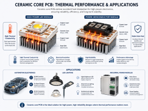
Ceramic core PCB is a printed circuit board built on a ceramic substrate instead of a conventional organic laminate such as FR4. In this type of board, the ceramic layer works as the main supporting base and thermal pathway. It gives the circuit strong heat transfer, stable electrical insulation, and excellent dimensional consistency under demanding operating conditions.

Unlike standard PCB materials that rely on glass fiber and resin, ceramic PCB boards use inorganic ceramic materials such as alumina, aluminum nitride, or silicon nitride. These materials are valued in high-power, high-frequency, high-temperature, and high-reliability electronics.

In the PCB industry, ceramic core PCB is often used for applications where ordinary laminates cannot provide enough thermal conductivity or long-term stability. The board may support thick copper, thin-film circuits, DPC copper plating, DBC bonding, or AMB structures, depending on the electrical and mechanical requirements of the project.

EBest Circuit (Best Technology) supports ceramic PCB manufacturing for engineers who need more than a basic circuit board. With experience in alumina PCB, aluminum nitride PCB, DPC ceramic PCB, DBC ceramic substrate, AMB ceramic substrate, and customized ceramic PCB boards, EBest Circuit helps customers move from early design review to production with practical engineering support.

What is the difference between ceramic and FR4?

Ceramic PCB and FR4 PCB are both widely used in electronics, but they are designed for different performance levels. FR4 is the most common PCB substrate because it is cost-effective, easy to process, and suitable for many consumer, industrial, and general electronic products. Ceramic PCB is selected when the circuit needs higher thermal conductivity, better temperature resistance, and stronger dimensional stability.

FR4 is made from woven fiberglass cloth and epoxy resin. It performs well in standard electronic assemblies, but its thermal conductivity is limited. Ceramic boards, by contrast, use inorganic ceramic substrates that conduct heat much more efficiently while keeping excellent insulation. This is why ceramic core PCB is commonly found in LED modules, laser equipment, power electronics, sensors, medical devices, automotive electronics, and aerospace-related systems.

ItemCeramic Core PCBFR4 PCB
Main materialAlumina, aluminum nitride, silicon nitride, or other ceramic materialsGlass fiber reinforced epoxy laminate
Thermal conductivityHigh, suitable for heat-sensitive and power applicationsLow to moderate, suitable for general electronics
Temperature resistanceExcellent stability at elevated temperaturesGood for standard operating environments
Mechanical behaviorHard, stable, and rigid, but requires careful handlingTougher and more flexible during standard assembly
Electrical insulationVery strong insulation performanceReliable insulation for common circuit designs
Typical applicationsHigh-power LEDs, RF modules, power devices, sensors, automotive electronicsConsumer electronics, control boards, communication devices, general PCBA
Cost levelHigher due to material and process complexityLower and highly scalable

The choice should not be based only on price. If the circuit generates a high amount of heat or must keep stable performance in a harsh environment, ceramic PCB can provide a stronger technical foundation.

What’s the difference between alumina PCB and aluminum nitride PCB?

Alumina PCB and aluminum nitride PCB are two of the most common ceramic PCB materials. Both provide good insulation, stable structure, and better thermal performance than FR4. The key difference is thermal conductivity. Alumina is widely used because it offers a balanced combination of price, process maturity, and electrical performance. Aluminum nitride is chosen when the design needs much higher heat dissipation.

Alumina PCB usually refers to ceramic boards made from aluminum oxide. Common grades include 96% alumina and 99.6% alumina. It is a practical choice for many LED, sensor, power module, and industrial electronic applications. It has good mechanical strength, stable electrical insulation, and a more accessible ceramic board price compared with aluminum nitride.

Aluminum nitride PCB is often used in more demanding thermal designs. Its thermal conductivity can be several times higher than alumina, making it highly suitable for power semiconductors, high-brightness LEDs, laser diodes, automotive power modules, and compact high-power assemblies. It is usually more expensive than alumina because the raw material, sintering process, and manufacturing control are more demanding.

ItemAlumina PCBAluminum Nitride PCB
MaterialAluminum oxide ceramicAluminum nitride ceramic
Thermal conductivityGood, commonly used for medium to high thermal needsExcellent, suitable for high-power heat dissipation
CostMore economical among ceramic PCB optionsHigher due to material and process requirements
Mechanical strengthStrong and mature in productionStrong, with careful process control needed
Electrical insulationExcellentExcellent
Typical useLED modules, sensors, heaters, industrial controls, power circuitsPower modules, laser devices, high-power LEDs, RF and automotive electronics

EBest Circuit can help customers compare ceramic PCB materials during DFM review, so the final design matches both technical needs and production cost targets.

Why use ceramic PCB?

Ceramic PCB is used because it solves several practical engineering problems at the same time. It helps remove heat, keeps circuits electrically insulated, supports high-density layouts, and performs well in high-temperature environments.

One of the strongest reasons to use ceramic PCB is thermal management. As electronic products become smaller and more powerful, heat has less room to escape. If heat remains around chips, LEDs, or power components, performance can drop over time. A ceramic board gives heat a faster path away from the source, helping the assembly work in a more stable condition.

Ceramic PCB also supports excellent electrical properties. It can provide low dielectric loss, high insulation resistance, and stable performance across demanding operating conditions. This is important for RF circuits, sensor modules, high-voltage electronics, and power devices.

  • High thermal conductivity for better heat spreading
  • Strong electrical insulation for compact circuit layouts
  • Excellent temperature resistance for harsh environments
  • Stable dimensions during thermal cycling
  • Good compatibility with power devices, LEDs, sensors, and RF modules
  • Long service life in high-reliability electronic products

For manufacturers, ceramic PCB also brings value in quality consistency. The substrate has stable physical properties, which helps reduce performance drift in precision electronics. For engineers, it allows a cleaner thermal design and can reduce the need for bulky heat sinks in some compact products.

How much does a ceramic PCB cost?

Ceramic PCB cost is usually higher than standard FR4 PCB cost because the material, processing method, copper bonding, laser drilling, metallization, and quality control are more specialized. In high-power or high-reliability products, better heat transfer and longer operating stability can reduce the risk of field problems and improve product performance.

The ceramic board price depends on several technical factors. Material selection is one of the biggest cost drivers. Alumina PCB is generally more economical, while aluminum nitride PCB costs more because it provides much higher thermal conductivity. Board size, thickness, copper thickness, circuit precision, via structure, surface finish, tolerance control, and production quantity also affect the final quotation.

Cost FactorHow It Affects Ceramic PCB Cost
Ceramic materialAlumina is usually more economical; aluminum nitride is higher in cost but stronger in thermal performance.
Board sizeLarger ceramic boards use more raw material and may require tighter handling control.
Substrate thicknessSpecial thickness requirements may increase material preparation and processing cost.
Copper thicknessThicker copper improves current capacity but increases plating or bonding complexity.
Line width and spacingFine circuits require more precise manufacturing control.
Via structureFilled vias, laser vias, and conductive vias can raise process complexity.
Surface finishENIG, immersion silver, nickel gold, or other finishes may affect pricing.
Order quantityPrototype cost per piece is higher; batch production usually improves unit cost.

For a reliable ceramic PCB quotation, engineers should provide Gerber files, drawings, material requirements, board thickness, copper thickness, surface finish, tolerance needs, and expected quantity. If the design is still being evaluated, EBest Circuit can review the technical requirements and suggest a practical manufacturing route before final pricing.

Can ceramic core PCB be customized in size and layout?

Yes, ceramic core PCB can be customized in size, layout, thickness, copper pattern, surface finish, and structure. Customization is one of the main reasons ceramic PCB is used in advanced electronic products.

Custom ceramic PCB does require careful design planning. Ceramic materials are hard and stable, but they are processed differently from FR4. Features such as hole size, edge shape, slot position, via design, copper thickness, and board outline should be reviewed before production. A strong DFM check helps improve manufacturability and keeps the finished board aligned with the original electrical and thermal goals.

Common customization options include:

  • Alumina PCB or aluminum nitride PCB substrate selection
  • Custom board outline, size, and ceramic thickness
  • Single-sided, double-sided, or multilayer ceramic PCB structure
  • Thin-film or thick-film circuit design
  • DPC, DBC, or AMB ceramic core manufacturing process
  • ENIG, nickel gold, silver, or other surface finish options
  • Laser drilling, via filling, and precision routing
  • Thick copper design for higher current carrying capacity

EBest Circuit works with customers on customized ceramic PCB projects where standard PCB materials may not deliver enough thermal or mechanical stability. The engineering team can assist with material selection, stack-up review, ceramic core manufacturing process evaluation, and production feasibility checks.

How are ceramic cores made?

Ceramic cores are made through a controlled process that starts with ceramic powder preparation and ends with a dense, stable substrate suitable for circuit formation. The exact process depends on the material and final PCB structure.

In a typical ceramic substrate process, ceramic powder is mixed with binders and additives to form a workable material. The material is shaped into sheets or pressed forms, then dried and sintered at high temperature. Sintering gives the ceramic its hardness, density, and stable physical properties. After that, the substrate may be lapped, polished, laser drilled, metallized, plated, etched, and finished according to the PCB design.

For circuit formation, different ceramic PCB technologies can be used. DPC, or Direct Plated Copper, is often chosen for fine circuits and high-precision designs. DBC, or Direct Bonded Copper, bonds copper directly onto the ceramic surface and is often used for power modules. AMB, or Active Metal Brazing, provides very strong bonding and is suitable for high-reliability power electronics.

Process TypeMain FeatureTypical Application
DPC ceramic PCBUses copper plating technology for fine circuits and precision patternsLED modules, sensors, optical devices, high-density ceramic circuits
DBC ceramic PCBDirect copper bonding provides strong thermal and current capacityPower modules, IGBT substrates, high-power electronics
AMB ceramic PCBActive brazing creates strong copper-to-ceramic bondingAutomotive power modules, high-reliability energy electronics
Thick-film ceramic PCBConductive paste is printed and fired onto ceramicHeaters, sensors, hybrid circuits, industrial modules
Thin-film ceramic PCBHigh-precision metal layers are deposited on ceramicMicrowave circuits, precision sensors, RF electronics

A professional ceramic PCB manufacturer must control material quality, sintering conditions, copper adhesion, surface flatness, circuit accuracy, and inspection standards. EBest Circuit combines process knowledge with practical PCB engineering support, helping customers choose the right ceramic core manufacturing process for the final product environment.

What thermal performance does ceramic core PCB deliver?

Ceramic core PCB delivers much stronger thermal performance than standard FR4 boards. The main advantage is that ceramic materials can transfer heat efficiently while still providing electrical insulation.

Alumina PCB offers good thermal conductivity for many industrial and LED applications. Aluminum nitride PCB provides a much higher level of heat transfer and is often used where thermal density is more demanding. With the right copper thickness, layout, and mounting structure, ceramic PCB boards can move heat away from components quickly and help maintain stable operating temperatures.

Thermal performance is not only about the ceramic material itself. The final result also depends on copper design, substrate thickness, dielectric path, via structure, solder joint quality, component placement, and heat sink contact.

MaterialGeneral Thermal PerformanceBest-Fit Applications
FR4Limited thermal conductivityGeneral electronics and low-to-medium power circuits
Alumina ceramicGood thermal conductivity with balanced costLEDs, sensors, industrial modules, moderate power electronics
Aluminum nitride ceramicExcellent thermal conductivityHigh-power LEDs, laser modules, power semiconductors, automotive electronics
Silicon nitride ceramicStrong thermal and mechanical reliabilityHigh-reliability power modules and harsh operating environments

For thermal-sensitive designs, EBest Circuit can support layout review and material comparison. This is helpful when customers need to decide between alumina PCB and aluminum nitride PCB, or when they want to optimize the balance between ceramic PCB cost, heat dissipation, and long-term reliability.

What are ceramic cores used for?

Ceramic cores are used in electronic products that need better thermal control, high insulation, stable structure, and reliable performance under demanding conditions. They are especially useful where compact size and high power must coexist. Because ceramic materials can transfer heat efficiently while maintaining electrical separation, they are widely used in modern power, lighting, automotive, medical, and communication systems.

In LED products, ceramic PCB helps move heat away from LED chips and supports stable brightness. In power electronics, ceramic substrates are used for modules that handle high current and high voltage. In RF and microwave circuits, ceramic materials can provide stable electrical characteristics. In medical and aerospace electronics, ceramic PCB boards support reliability, precision, and long service life.

  • High-power LED modules and lighting engines
  • Laser diode modules and optical devices
  • Power semiconductor packages and IGBT modules
  • Automotive electronics and electric vehicle power modules
  • RF, microwave, and communication circuits
  • Medical sensors and monitoring devices
  • Industrial control modules and high-temperature electronics
  • Aerospace, UAV, and high-reliability electronic assemblies

Ceramic core PCB is a strong choice when the product needs more than ordinary PCB performance. Alumina PCB is suitable for balanced thermal and cost requirements, while aluminum nitride PCB is ideal for stronger heat dissipation. For custom ceramic PCB boards, ceramic PCB materials, ceramic PCB cost evaluation, and ceramic core manufacturing process support, EBest Circuit (Best Technology) can help engineers build a practical path from prototype to production.

Summary:

Ceramic core PCB is not simply a premium version of FR4. It is a specialized circuit platform for products that need excellent heat transfer, high insulation, stable operation, and compact design. If your project requires alumina PCB, aluminum nitride PCB, or custom ceramic PCB manufacturing support, you can contact sales@bestpcbs.com for project discussion and quotation support.

You may also like

Ceramic Substrate PCB Manufacturer Design & Prototype| Fast Delivery, Custom Solutions

March 30th, 2026

Why Choose EBest for Your Ceramic Substrate PCB Needs?

EBest stands as your premier choice for Ceramic Substrate PCB manufacturing and prototyping. We deliver unmatched lead times, rigorous quality control, industry-leading certifications, and comprehensive support throughout your project. Our commitment to excellence ensures your Ceramic Substrate PCB projects are completed efficiently, reliably, and to the highest standards.

  • Fast Delivery: Industry-leading turnaround times for prototypes and mass production, meeting your critical project deadlines.
  • Superior Quality: Precision manufacturing with zero-defect tolerance, ensuring optimal performance and long-term reliability.
  • Certified Excellence: Compliant with ISO 9001, IPC-A-600, and other international quality and safety standards.
  • Expert Support: A dedicated engineering team provides end-to-end technical assistance, from design to delivery.

What is a Ceramic Substrate PCB?

A Ceramic Substrate PCB is a specialized printed circuit board that uses ceramic materials (such as alumina Al₂O₃, aluminum nitride AlN, or silicon nitride Si₃N₄) as its base insulating layer instead of traditional organic materials like FR-4. These boards are engineered to excel in high-temperature, high-power, and high-frequency electronic applications where standard PCBs fail. The ceramic substrate provides exceptional thermal conductivity, electrical insulation, and mechanical stability, making it indispensable for modern, demanding electronics.

Ceramic Substrate PCB

Ceramic Substrate PCB Stackup

LayerMaterialThickness (Typical)Function
Top CopperElectrodeposited Copper1–5 oz (35–175 ÎŒm)Conductive traces, pads, and planes
Ceramic CoreAlumina (Al₂O₃) / Aluminum Nitride (AlN)0.25–2.0 mmInsulation, thermal management, structural support
Bottom CopperElectrodeposited Copper1–5 oz (35–175 ÎŒm)Conductive traces, pads, and planes
Surface FinishENIG / Immersion Silver / OSP0.05–0.5 ÎŒmProtect copper, improve solderability

Note: Multilayer ceramic substrate PCBs (LTCC/HTCC) feature alternating ceramic and conductive layers, typically up to 10–20 layers for high-density integration.

Ceramic Substrate PCB Manufacturing Process

Step 1: Ceramic Substrate Preparation

High-purity ceramic powders (Al₂O₃, AlN) are pressed into green sheets, precisely cut to size, and sintered at ultra-high temperatures (1,600–1,800°C) to form dense, rigid substrates with consistent material properties.

Step 2: Metallization & Circuit Patterning

Copper is bonded to the ceramic surface using advanced processes:

  • DBC (Direct Bonded Copper): Copper foil is fusion-bonded to ceramic at ~1,065°C.
  • DPC (Direct Plated Copper): Copper is electroplated onto a sputtered seed layer for fine-line precision.

Photolithography and etching define the circuit pattern, creating high-resolution traces and pads.

Step 3: Via Formation & Plating

Micro-vias are created using laser drilling for precision. The via walls are metallized through electroplating to establish vertical electrical connections between layers, critical for thermal and signal paths.

Step 4: Surface Treatment & Finishing

The board undergoes surface finishing (ENIG, immersion silver, etc.) to protect the copper circuitry and ensure reliable solderability during component assembly.

Step 5: Testing & Quality Assurance

Each Ceramic Substrate PCB undergoes rigorous electrical testing (continuity, insulation resistance), thermal cycling, and visual inspection to guarantee compliance with specifications and performance standards.

Ceramic Substrate PCB Design Guide

Designing a Ceramic Substrate PCB requires specialized knowledge to overcome inherent material challenges. Key pain points include material brittleness, CTE mismatch with components, thermal management, and fine-line manufacturing constraints. EBest’s engineering team provides expert guidance to navigate these challenges and optimize your design for success.

Key Design Considerations & Solutions

Material Compatibility & CTE Matching

  • Pain Point: A significant CTE mismatch between ceramic (5–7 ppm/°C) and silicon (4.5 ppm/°C) causes thermal stress, leading to solder joint fatigue and substrate cracking.
  • Solution: Select AlN (CTE ~4.5 ppm/°C) for silicon-based high-power devices. Use compliant materials and underfill in assembly to absorb stress.

Thermal Management Optimization

  • Pain Point: Inefficient heat dissipation leads to hotspots and component failure in high-power designs.
  • Solution: Maximize copper thickness in power paths, integrate thermal vias, and use large copper planes for heat spreading. AlN substrates offer 8–10x higher thermal conductivity than alumina.

Mechanical Stress & Fragility

  • Pain Point: Ceramic brittleness causes chipping and cracking during handling, assembly, or thermal cycling.
  • Solution: Avoid sharp corners; use rounded geometries. Design generous tolerances (+/–0.1 mm) and avoid V-cuts. Use robust panelization with thick connecting tabs.

Fine-Line & High-Density Design

  • Pain Point: Achieving fine line widths/spacing (<50 ÎŒm) is challenging with standard processes.
  • Solution: Utilize DPC technology for line widths down to 15 ÎŒm. Collaborate with EBest early for DFM analysis to ensure design manufacturability.

For flawless Ceramic Substrate PCB design, partner with EBest. Our experts provide complimentary DFM reviews and design optimization to ensure your project is built for performance and reliability.

Ceramic Substrate PCB Prototype: Rapid, Reliable, Custom

Prototyping Ceramic Substrate PCBs presents unique hurdles: long lead times, high costs, and difficulty in achieving consistent quality with low volumes. EBest specializes in rapid, high-quality Ceramic Substrate PCB prototyping, eliminating these barriers and accelerating your product development cycle.

Prototype Challenges & Our Solutions

Long Lead Times for Custom Prototypes

  • Challenge: Traditional ceramic PCB prototyping can take weeks, delaying product validation.
  • Solution: EBest offers rapid prototype services with industry-leading turnaround times, getting your boards in hand quickly.

High Cost for Low-Volume Runs

  • Challenge: High tooling and setup costs make small-batch prototyping prohibitively expensive.
  • Solution: We maintain flexible manufacturing lines optimized for low-volume, high-mix production, keeping prototype costs competitive.

Inconsistent Prototype Quality

  • Challenge: Achieving the same material and process quality in prototypes as in mass production is difficult.
  • Solution: Our prototypes use the exact same materials and production processes as full-scale manufacturing, ensuring reliable performance data.

Limited Design Iteration

  • Challenge: Cost and time constraints limit the number of design iterations possible.
  • Solution: Our efficient prototyping process allows for multiple design iterations, enabling you to refine and perfect your design before full production.

Trust EBest for your Ceramic Substrate PCB prototyping needs. We deliver fast, affordable, and production-quality prototypes to validate your design and accelerate your time-to-market.

How to Choose Ceramic Substrate PCB Raw Materials

Selecting the right ceramic material is critical for balancing performance, cost, and application suitability. The table below compares the most common materials:

MaterialThermal Conductivity (W/m·K)CTE (ppm/°C)Dielectric Constant (Δr)Key Applications
Alumina (96% Al₂O₃)20–25~7.09.5Consumer electronics, industrial control, LED lighting
Alumina (99% Al₂O₃)28–30~7.09.8Automotive electronics, medical devices, telecom
Aluminum Nitride (AlN)170–230~4.58.8High-power semiconductors, RF, EV power modules
Silicon Nitride (Si₃N₄)80–100~3.27.8Automotive, aerospace, high-reliability industrial

Ceramic Substrate PCB Applications

Ceramic Substrate PCBs are the backbone of high-performance electronics across critical industries, enabling innovation where thermal, electrical, and reliability demands are extreme.

Automotive Electronics

Ceramic Substrate PCBs are essential in electric vehicle (EV) powertrains, including IGBT modules, on-board chargers (OBC), and LED headlight drivers. They withstand extreme under-hood temperatures (-40°C to 150°C) and provide superior thermal management for high-voltage, high-power systems.

Communication & 5G Infrastructure

In 5G base stations, RF power amplifiers, and microwave systems, Ceramic Substrate PCBs (especially AlN) offer low dielectric loss and excellent thermal stability, ensuring signal integrity and efficient heat dissipation for high-frequency, high-power operation.

Industrial Automation & Power Electronics

Used in variable-frequency drives (VFDs), servo controls, and power supplies, these boards handle high power densities and harsh industrial environments. Their excellent thermal conductivity and mechanical strength ensure reliable operation in continuous-duty applications.

Medical Devices

Ceramic Substrate PCBs are used in precision medical equipment like ultrasound systems, patient monitors, and surgical lasers. They offer biocompatibility, high electrical insulation, and the ability to withstand repeated sterilization cycles, meeting strict medical device standards.

What Are the Key Advantages of Ceramic Substrate PCB Over FR4?

Ceramic Substrate PCBs offer transformative advantages over traditional FR-4 PCBs, particularly in high-performance applications. Key benefits include:

  • Superior Thermal Conductivity: Up to 1,000x higher than FR-4, enabling efficient heat dissipation.
  • Excellent Electrical Insulation: High dielectric strength prevents short circuits in high-voltage applications.
  • Extreme Temperature Resistance: Operates reliably from -50°C to over 350°C.
  • Mechanical Stability: High rigidity and resistance to warping under thermal stress.
  • Chemical Inertness: Resistant to most chemicals, ideal for harsh environments.

How Does Thermal Conductivity Impact Ceramic Substrate PCB Performance?

Thermal conductivity is the defining performance metric for Ceramic Substrate PCBs. It directly determines the board’s ability to dissipate heat generated by power components. Higher thermal conductivity (e.g., AlN at 200 W/m·K vs. alumina at 25 W/m·K) allows for:

  • Higher power density designs in smaller form factors.
  • Lower component operating temperatures, significantly increasing reliability and lifespan.
  • Elimination of bulky heat sinks, enabling more compact and efficient product designs.

What Are the Common Failure Modes in Ceramic Substrate PCBs?

The primary failure modes stem from thermal and mechanical stress:

  • Thermal Fatigue: CTE mismatch causes cyclic stress, leading to solder joint cracking or substrate delamination.
  • Mechanical Fracture: Brittleness leads to cracking from shock, vibration, or improper handling.
  • Metallization Degradation: Oxidation or poor adhesion of the copper layer causes open circuits.
  • Thermal Runaway: Inadequate heat dissipation leads to overheating and catastrophic failure.

Can Ceramic Substrate PCBs Be Used for High-Frequency Applications?

Absolutely. Ceramic Substrate PCBs, especially AlN and high-purity alumina, are ideal for high-frequency (RF/microwave) applications. They offer:

  • Low Dielectric Loss (tan ÎŽ): Minimizes signal attenuation and power loss.
  • Stable Dielectric Constant: Ensures consistent signal propagation across temperature variations.
  • Excellent High-Frequency Performance: Supports frequencies up to mmWave bands for 5G and radar systems.

What Is the Difference Between DBC and DPC Ceramic Substrate PCB?

DBC (Direct Bonded Copper) and DPC (Direct Plated Copper) are the two primary manufacturing technologies:

  • DBC: Copper foil is fusion-bonded to ceramic at high temperature. It is best for thick copper (up to 10 oz) and high-power applications. It offers excellent thermal performance but limited line resolution (~100 ÎŒm).
  • DPC: Copper is electroplated onto a sputtered seed layer. It enables ultra-fine line widths (<15 ÎŒm) for high-density, high-frequency designs. It is ideal for complex, miniaturized circuits.

Ceramic Substrate PCB FAQ

Q1: What is the maximum operating temperature for a Ceramic Substrate PCB?

A1: Ceramic Substrate PCBs can reliably operate at continuous temperatures up to 350°C, with short-term peaks exceeding 500°C—far exceeding the limits of FR-4.

Q2: Can you manufacture flexible Ceramic Substrate PCBs?

A2: While inherently rigid, specialized ceramic composites and LTCC (Low-Temperature Co-fired Ceramic) technologies can produce semi-flexible or 3D-shaped Ceramic Substrate PCBs for specific applications.

Q3: What is the minimum line width/spacing achievable?

A3: Using DPC technology, EBest can achieve line widths and spacing as fine as 15 ÎŒm, enabling high-density circuit designs.

Q4: Are Ceramic Substrate PCBs suitable for mass production?

A4: Yes. EBest operates automated production lines capable of high-volume, consistent manufacturing of Ceramic Substrate PCBs for industrial and automotive applications.

Q5: How do I get a quote for my Ceramic Substrate PCB project?

A5: Contact our sales team with your Gerber files, BOM, layer stackup, quantity, and target delivery date. We provide detailed, competitive quotes quickly.

Q6: What surface finishes are available for Ceramic Substrate PCBs?

A6: We offer ENIG (Electroless Nickel Immersion Gold), immersion silver, and OSP (Organic Solderability Preservative) to meet various assembly and reliability requirements.

Q7: Can you assemble components on Ceramic Substrate PCBs?

A7: Yes, EBest provides full turnkey services, including high-precision SMT and through-hole component assembly for Ceramic Substrate PCBs.

Ready to Start Your Ceramic Substrate PCB Project?

EBest is your trusted partner for all Ceramic Substrate PCB design, prototyping, and manufacturing needs. With our technical expertise, fast delivery, and commitment to quality, we ensure your project succeeds. Contact us today to discuss your requirements and get a free quote.

Email: sales@bestpcbs.com

You may also like

Ceramic PCB Design Guideline, Ceramic PCB Manufacturing Process

March 26th, 2026

Many electronic products now run hotter, smaller, and faster than before. That shift makes thermal design more important than ever. In many cases, standard FR4 works well. But when heat becomes harder to manage, ceramic substrates offer a more dependable path. With thermal conductivity that can reach 20 to 30 W/m·K for alumina and around 170 to 200 W/m·K for aluminum nitride, ceramic materials are often selected for power modules, LED lighting, RF products, and automotive electronics.

n this guide, you will learn what ceramic PCB design means, which materials are commonly used, how ceramic boards are manufactured, and how to choose between ceramic PCB and FR4 for different applications.

What Is Ceramic PCB Design?

Ceramic PCB design refers to the process of creating a printed circuit board on a ceramic substrate instead of a traditional FR4 base. In this type of board, the substrate does more than support the circuit. It also helps with heat transfer, insulation, and structural stability.

That is why ceramic PCB design is often used in applications where thermal control matters. A well-designed ceramic board can help reduce hot spots, support stable electrical performance, and improve product life in compact or high-power environments.

Typical application areas include:

  • High-power LED modules
  • Power semiconductor circuits
  • RF and microwave products
  • Automotive control systems
  • Medical and industrial electronics
Ceramic PCB Design

Ceramic PCB Design

Why Choose Ceramic PCBs?

Ceramic PCBs are widely used because they combine heat dissipation and electrical insulation in one structure. This can make the full product design more efficient, especially in space-limited applications. Main advantages include:

  • Better heat dissipation than standard FR4
  • Stable performance under temperature cycling
  • Strong electrical insulation
  • Good dimensional stability
  • Suitable for compact and high-density layouts

For many engineers, the main attraction is thermal performance. Standard FR4 is usually around 0.3 W/m·K, which is enough for many general products. But for higher heat loads, ceramic substrates offer a clear improvement.

Why Choose Ceramic PCBs?

Why Choose Ceramic PCBs?

Common Materials Used in Ceramic PCB Design

Choosing the right ceramic pcb material is one of the first decisions in the design process. Different materials offer different thermal and mechanical properties.

MaterialThermal ConductivityCost LevelTypical Use
Al2O320–30 W/m·KLowerLED, sensors, control boards
AlN170–200 W/m·KHigherPower modules, RF, high-heat products
Si3N470–90 W/m·KHigherHigh-reliability power electronics
BeOVery highHighSpecial industrial applications

In most commercial projects, the main decision is between Al2O3 and AlN.

Al2O3 vs AlN: Which One Is Suitable for Your Ceramic PCB Project?

Both materials are common in ceramic PCB design, but they fit different needs.

PropertyAl2O3AlN
CostMore economicalHigher
Thermal ConductivityModerateVery high
AvailabilityBroadMore specialized
Best ForGeneral ceramic circuitsHigh-power thermal applications

A simple selection logic is:

  1. Choose Al2O3 when you need a practical ceramic solution with balanced cost and performance.
  2. Choose AlN when your board must remove heat faster or work in a tighter thermal environment.
  3. Review the total thermal path before making the final decision.

If the product is compact, sealed, or power-dense, AlN often provides more design margin. If the thermal load is moderate, Al2O3 is often the more economical choice.

Ceramic PCB vs FR4 PCB: What’s the Difference?

The discussion around ceramic pcb vs fr4 is common because both materials serve important roles.

AspectCeramic PCBFR4 PCB
Thermal ConductivityHigherLower
Heat ResistanceBetterModerate
Dimensional StabilityStrongStandard
Mechanical NatureHarder, more brittleTougher, more flexible
CostHigherLower
Typical UsePower, RF, LEDGeneral electronics

In short:

  • FR4 is suitable for standard and cost-sensitive electronics.
  • Ceramic PCB is more suitable for high-heat and high-reliability designs.

So the real question is not which one is better overall, it based on which one fits your product conditions better.

Ceramic PCB Design Guidelines

Ceramic PCB design is not simply FR4 layout on a different substrate. The material behaves differently in thermal transfer, mechanical strength, copper bonding, and assembly response. If these factors are considered early, the board is easier to manufacture and more stable in use.

1. Start with thermal goals, not only electrical layout

Most ceramic PCB projects begin because heat is already a concern. So the design should first identify where the heat is generated, how much power is lost, and where that heat will go next.

A practical design review usually includes:

  • heat source location
  • power density of major components
  • thermal path from device to substrate
  • interface to heat sink or housing
  • operating ambient temperature

For example, if a board carries LED chips, power ICs, or RF devices, placing those parts without a clear heat path can waste the thermal advantage of the ceramic substrate.

2. Choose the right ceramic material for the real operating condition

Material selection affects the whole design window. Al2O3 is widely used because it offers good insulation, mature processing, and reasonable cost. AlN is better when the thermal load is higher and the product has less room for heat buildup.

This choice should match the actual project target, not only the material data sheet. A low-power control board and a compact power module should not use the same logic.

3. Match copper layout with current, heat, and process capability

Copper traces on ceramic boards should be designed with three things in mind:

  • current carrying ability
  • heat spreading
  • manufacturability

Very narrow traces may look efficient in layout, but they are not always ideal for yield or long-term reliability. Wider copper areas can help thermal spreading, but overly large copper imbalance may create stress during heating and cooling cycles.

4. Pay close attention to pad design and solder joint reliability

Pad design matters more than many designers expect. Ceramic substrates are rigid, and the expansion behavior differs from FR4. That means poor pad design can affect solder joint stability, especially in power devices or larger packages.

It is wise to check:

  • pad size versus component package
  • solder fillet space
  • thermal pad design
  • copper symmetry around large pads
  • assembly method and reflow profile

This is especially important for LED chips, bare die, power packages, and ceramic-mounted RF parts.

5. Consider brittleness in the mechanical design

Ceramic offers excellent stability, but it is also more brittle than FR4. That means the board design should avoid stress concentration.

Important mechanical points include:

  • leave enough clearance from holes to edges
  • avoid weak narrow bridges in the outline
  • reduce sharp internal corners where possible
  • design mounting areas with even force distribution
  • avoid layout features too close to cut edges

In short, ceramic PCB design should not only perform well electrically. It should also survive handling, assembly, fastening, and real product use.

6. Align the design with the selected manufacturing process

This point is often overlooked. Ceramic PCB design should always match the actual process route. If the board will be made by DPC ceramic PCB technology, then line width, spacing, via structure, copper thickness, and surface finish should all follow DPC process capability.

That is why early communication with the manufacturer is valuable. A design that fits the real process window usually moves to production faster and with fewer revisions.

Ceramic PCB Manufacturing Processes

There are several ceramic PCB manufacturing methods, but for projects that require fine lines, good adhesion, and precise circuit definition, DPC ceramic PCB is a widely used option. DPC stands for Direct Plated Copper. This process forms the copper circuit directly on the ceramic substrate through thin film metallization and copper plating steps.

Compared with thick film processes, DPC is often preferred for finer circuit patterns and more controlled conductor formation. It is commonly used in LED packaging, RF modules, sensors, and high-precision ceramic circuit applications.

DPC Ceramic PCB Manufacturing Flow

Here is the typical DPC ceramic PCB manufacturing process:

Ceramic PCB Manufacturing Processes

1. Ceramic substrate preparation

    The process begins with the selected ceramic substrate, usually Al2O3 or AlN. The surface must be cleaned carefully to remove particles, oil, and contamination. This step is important because good surface condition helps the following metal layer bond more reliably.

    2. Thin film metallization

    A thin metal seed layer is deposited on the ceramic surface. This layer often includes metals such as titanium, copper, or other adhesion and conductive layers depending on the process design. Its role is to provide a base for later copper plating.

    3. Photoresist coating

    A photoresist layer is applied to the metallized ceramic surface. This creates the imageable layer used to define the circuit pattern.

    4. Exposure and development

    The circuit image is transferred onto the photoresist by exposure. After development, the required copper pattern area is opened, while the rest remains protected.

    5. Copper electroplating

    Copper is plated onto the exposed circuit areas until the target thickness is reached. This step builds the actual conductive traces and pads. The plating thickness is controlled based on current requirement, pattern accuracy, and product application.

    6. Resist stripping

    After plating is completed, the remaining photoresist is removed. At this stage, the plated copper pattern remains on the substrate.

    7. Seed layer etching

    The exposed thin seed layer that is no longer needed is etched away. This leaves only the final circuit pattern on the ceramic substrate.

    8. Surface finish treatment

    A suitable surface finish is applied to improve solderability, bonding performance, or corrosion resistance. Common finishes depend on the product design and assembly method.

    9. Laser drilling or shaping if needed

    If the design requires slots, openings, or special board outlines, laser or precision machining processes are used. Ceramic substrates need careful shaping because the material is hard and brittle.

    10. Final inspection and testing

      The finished board goes through dimensional inspection, circuit inspection, adhesion testing, and appearance review. For higher-end applications, extra checks may include thermal cycling, insulation performance, and bonding quality verification.

      Applications of Ceramic PCB Design

      Ceramic PCB design is widely used in products that need strong thermal performance and stable operation over time.

      Common applications include:

      • LED lighting modules
      • Automotive electronics
      • Power control systems
      • RF and microwave devices
      • Medical equipment
      • Industrial power modules
      • Laser and communication products

      In high-power LED systems, ceramic substrates help transfer heat away from the LED source. In automotive and industrial electronics, they support more stable operation under repeated thermal cycling.

      Applications of Ceramic PCB Design

      Applications of Ceramic PCB Design

      Why Choose EBest Circuit for Ceramic PCB Design?

      With 20+ years of PCB and PCBA experience, EBest Circuit supports customers from early design review to full production. We have served 10,000+ engineers and 1,800+ customers, giving us broad experience across thermal management, high-reliability electronics, and complex PCB structures.

      Why many customers choose EBest Circuit for ceramic PCB design:

      • 20+ years of manufacturing experience in PCB and PCBA
      • Support for advanced materials, including Al2O3 ceramic PCB and AlN ceramic PCB
      • Engineering-driven support with free DFM review and process suggestions
      • One-stop capability from PCB fabrication to PCBA assembly and testing
      • Fast response for prototype and small-batch projects
      • Quality systems supported by ISO 9001, ISO 13485, IATF 16949, and AS9100D
      • MES-based traceability for better process control and production visibility

      We also understand that ceramic PCB projects are often tied to demanding applications such as LED lighting, power electronics, RF devices, and industrial controls. In these products, stable quality and process consistency are just as important as thermal performance on paper. That is why we focus on both engineering review and manufacturing control.

      If you need a ceramic PCB manufacturer that can support design optimization, material selection, and reliable production, EBest Circuit is ready to help. For project discussion or quotation, please contact sales@bestpcbs.com.
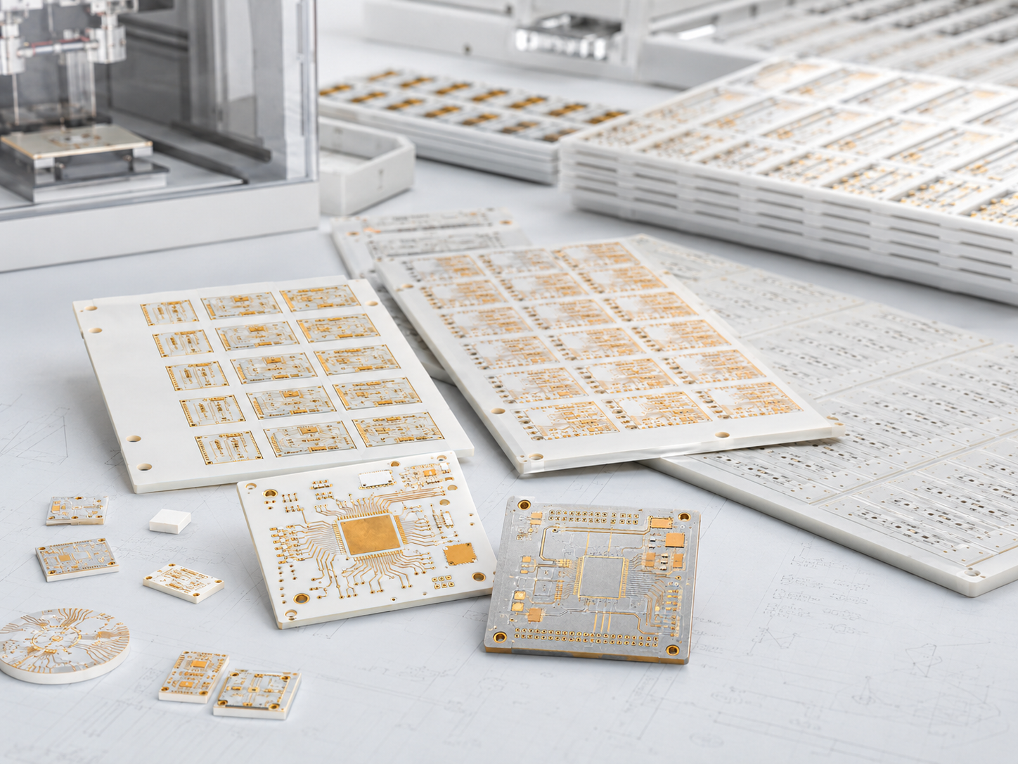
      FAQs About Ceramic PCB Design

      1. What is ceramic PCB design used for?

        Ceramic PCB design is used for electronic products that need better heat dissipation, strong insulation, and stable operation in demanding environments.

        2. Which ceramic pcb material is most common?

        Al2O3 is one of the most common materials because it offers a good balance of cost and performance.

        3. When should I choose AlN?

        AlN is a better choice when the design has high heat density or requires faster heat transfer.

        4. Is ceramic PCB better than FR4?

        For thermal-intensive applications, ceramic is usually a better option. For standard electronics, FR4 is often enough.

        5. Can a ceramic pcb manufacturer help optimize my design?

        Yes. Early design review can improve manufacturability, reduce risk, and shorten project cycles.

        6. Are ceramic PCBs suitable for LED products?

        Yes. They are widely used in high-power LED modules because heat dissipation is critical.

        You may also like

        Factors to Consider When Choosing Ceramic Substrates

        March 18th, 2026

        Understanding factors to consider when choosing ceramic substrates is critical for device performance and reliability. This guide covers all essential factors to consider when choosing ceramic substrates for professional engineering applications.

        Ceramic Substrates

        What are the key factors to consider when choosing ceramic substrates?

        The most important factors include thermal, electrical, mechanical, material, and application compatibility.

        These elements directly decide performance, stability, and service life.

        Selecting correctly avoids failures in high‑demand environments.

        • Thermal conductivity and thermal expansion
        • Dielectric constant and insulation performance
        • Mechanical strength and structural stability
        • Material type and manufacturing compatibility
        • Quality, supply chain, and delivery

        How do material properties affect ceramic substrate selection?

        Material properties form the foundation of ceramic substrate performance.

        Mismatched properties lead to overheating, signal loss, or mechanical breakage.

        Each parameter must align with your application needs.

        Thermal conductivity requirements

        Higher thermal conductivity improves heat dissipation for high‑power devices.

        It keeps components cool and extends service life.

        This is non‑negotiable for power and automotive electronics.

        Dielectric and insulation performance

        Dielectric constant impacts signal integrity.

        High insulation prevents leakage in high‑voltage systems.

        Low dielectric loss improves energy efficiency.

        Which thermal factors matter most for ceramic substrates?

        Thermal performance ensures long‑term stability under load and temperature cycles.

        Poor thermal design causes cracking, warping, and early failure.

        Thermal matching is vital for reliable assembly.

        • Coefficient of thermal expansion (CTE) matching
        • Thermal cycling stability
        • High temperature resistance
        • Heat dissipation path design
        • Compatibility with thermal interface materials

        How to match electrical requirements for ceramic substrates?

        Electrical properties protect circuits and ensure signal quality.

        They prevent interference and breakdown in demanding environments.

        Correct values keep systems safe and stable.

        Insulation resistance

        High insulation resistance supports high‑voltage applications.

        It reduces risk of short circuits and electrical failures.

        Critical for power electronics and industrial controls.

        Dielectric loss

        Low dielectric loss improves efficiency in high‑frequency devices.

        It reduces heat from signal transmission.

        Ideal for communication and server equipment.

        What mechanical standards should ceramic substrates meet?

        Mechanical strength prevents breakage during production and use.

        It supports handling, assembly, and harsh environments.

        Strong substrates maintain dimensional stability.

        • Bending strength
        • Fracture toughness
        • Hardness and wear resistance
        • Dimensional accuracy
        • Thermal shock resistance

        How to compare common ceramic substrate materials

        How to compare common ceramic substrate materials?

        The table below helps you choose based on performance and application.

        MaterialThermal Conductivity (W/m·K)Dielectric ConstantTypical Applications
        Alumina (Al₂O₃)20–309.8Consumer electronics, LED
        Aluminum Nitride (AlN)170–2308.8Automotive, power electronics
        Silicon Nitride (Si₃N₄)20–907.0High‑power devices
        Zirconia (ZrO₂)2–325.0Medical devices, sensors

        Which industries use ceramic substrates most widely?

        Ceramic substrates perform best in four high‑growth industries.

        Automotive electronics

        AlN substrates handle heat in EV power modules.

        They withstand vibration and extreme temperatures.

        Ensure stable performance in motor controls.

        Medical electronics

        High‑purity alumina offers biocompatibility and insulation.

        It meets strict medical standards for monitoring devices.

        Safe for long‑term implantable and diagnostic tools.

        LED & power electronics

        Ceramic substrates improve heat dissipation for LEDs.

        They extend lifespan and boost brightness.

        Widely used in industrial and outdoor lighting.

        Aerospace & industrial control

        Special ceramics resist extreme temperatures and corrosion.

        They meet aerospace reliability standards.

        Stable in automation and harsh factory environments.

        How to ensure processing compatibility of ceramic substrates?

        Processing compatibility lowers production difficulty and cost.

        Good metallization and bonding support strong assembly.

        Stable processing ensures consistent yields.

        • Machinability
        • Metal layer adhesion
        • Solderability and bonding strength
        • Compatibility with standard PCB processes
        • Tolerance control

        How to judge ceramic substrate quality and reliability?

        Quality control prevents inconsistent performance and failures.

        Certified materials and testing ensure long service life.

        Reliable substrates reduce maintenance and replacement cost.

        • Raw material purity
        • Dimensional accuracy
        • Thermal cycle testing
        • Insulation and voltage testing
        • Compliance with international standards

        Why supply chain & delivery matter for ceramic substrates?

        Stable supply avoids production delays and shortages.

        On‑time delivery keeps projects on schedule.

        Consistent quality supports mass production.

        • Steady raw material supply
        • On‑time delivery capability
        • Full quality traceability
        • Professional technical support
        • Mass production capacity

        Can ceramic substrates be customized for special uses?

        Customization meets unique design and performance needs.

        Tailored materials, sizes, and structures fit special equipment.

        Custom solutions improve overall device efficiency.

        • Custom material formulas
        • Special thickness and shape
        • Modified thermal or electrical properties
        • Application‑specific metallization
        • Unique packaging requirements

        FAQ: Top questions about factors to consider when choosing ceramic substrates

        What factors to consider when choosing ceramic substrates?

        Key factors include thermal performance, electrical properties, mechanical strength, material type, quality, supply chain, and application compatibility.

        Which ceramic substrate is best for high power?

        Aluminum nitride (AlN) is best for high power due to ultra‑high thermal conductivity.

        How to ensure thermal reliability of ceramic substrates?

        Match thermal expansion coefficients and use high‑thermal‑conductivity materials.

        What is the difference between AlN and alumina substrates?

        AlN has much higher thermal conductivity; alumina offers cost‑effective general use.

        Can ceramic substrates be used in medical devices?

        Yes, high‑purity alumina is widely used for biocompatibility and stability.

        How to select a reliable ceramic substrate supplier?

        Check quality system, delivery stability, technical support, and supply chain.

        Are ceramic substrates customizable for special applications?

        Yes, materials, dimensions, and performance can be customized for specific needs.

        Conclusion

        All factors to consider when choosing ceramic substrates must be evaluated together.

        The right choice improves performance, reliability, and product stability.

        Professional selection supports long‑term success in high‑end electronics.

        EBest provides premium ceramic substrates with stable supply, strict quality control, and professional support. For orders and inquiries, contact us at: sales@bestpcbs.com

        You may also like

        What is Empty Circuit Board? Empty Circuit Board vs Assembled PCB

        March 5th, 2026

        An empty circuit board is the starting point of almost every electronic product. Before chips, resistors, and connectors appear on a board, engineers begin with a bare platform that carries electrical pathways and mechanical structure. This base platform is the empty circuit board, also called a bare PCB.

        EBest Circuit (Best Technology) has more than 19 years of PCB fabrication and assembly experience. Our engineering team supports projects from design review to final assembly. With integrated PCB fabrication and PCBA production, customers receive consistent quality, fast delivery, and practical engineering support throughout the process.

        What Is an Empty Circuit Board?

        An empty circuit board refers to a printed circuit board before electronic components are mounted. It contains copper traces, vias, pads, and insulating substrate materials. These elements form the electrical network that later connects components.

        In manufacturing terms, an empty circuit board is often called:

        • Bare PCB
        • Blank PCB
        • Fabricated PCB

        The board becomes a finished electronic module only after component assembly. That stage is known as PCBA (Printed Circuit Board Assembly).

        What Materials Are Used in an Empty Circuit Board?

        The materials inside an empty circuit board determine electrical performance and durability. Most boards combine insulating substrate materials with conductive copper layers.

        1. Substrate Materials

        The substrate forms the structural foundation of the PCB. Common substrate materials include:

        • FR4 fiberglass epoxy – the most widely used PCB material
        • High-TG FR4 – suitable for higher thermal environments
        • Polyimide – used for flexible circuits
        • Aluminum core – used for heat dissipation
        • Ceramic materials – used in high-frequency electronics

        Among these options, FR4 remains the standard choice because it balances cost, strength, and electrical insulation.

        2. Copper Layers

        Copper forms the conductive pathways on the board. These traces connect electronic components. Copper thickness is measured in ounces (OZ) per square foot. Typical copper thickness values include:

        Copper WeightThicknessApplication
        0.5 oz~17 ”mFine-line circuits
        1 oz~35 ”mStandard electronics
        2 oz~70 ”mPower electronics
        3 oz+100 ”m+High-current circuits

        Higher copper thickness improves current capacity and thermal performance.

        3. Solder Mask

        Solder mask is the colored protective layer on top of the PCB. It prevents solder bridging during assembly. Common colors include:

        • Green
        • Black
        • Blue
        • White
        • Red

        Green remains the most common color because it offers good contrast for inspection.

        4. Surface Finish

        The copper pads require protective coating. Surface finishes prevent oxidation and improve solderability. Typical finishes include:

        • HASL (Hot Air Solder Leveling)
        • ENIG (Electroless Nickel Immersion Gold)
        • ENEPIG
        • Immersion silver
        • OSP coating

        Each finish has advantages depending on product requirements.

        How Is an Empty Circuit Board Manufactured?

        Manufacturing an empty circuit board involves multiple precision processes. Each step builds part of the board structure. Below is a simplified overview of the process.

        1. Design File Preparation

        Engineers prepare design files using PCB design software. These files define trace routing, drill holes, and board dimensions. Typical design files include:

        • Gerber files
        • Drill files
        • Stack-up specifications

        2. Material Preparation

        3. Inner Layer Imaging

        4. Etching

        5. Lamination

        6. Drilling

        7. Copper Plating

        8. Solder Mask Application

        9. Surface Finish

        10. Electrical Testing

        If you want to know more the manufacturing process of empty circuit board, you can watch below video from our PCB fabrication workshop:

        What Are the Different Types of Empty Circuit Boards?

        Empty circuit boards are not all built the same. Engineers select different PCB structures based on circuit complexity, signal speed, thermal conditions, and mechanical requirements. Below are the most common types of empty circuit boards used in modern electronics manufacturing.

        1. Single-Layer Empty Circuit Board

          A single-layer circuit board contains one conductive copper layer on one side of the substrate. All components and traces appear on the same surface.

          Typical applications include:

          • LED lighting modules
          • Power adapters
          • Small household electronics
          • Simple control boards

          However, routing space is limited because all connections must exist on one layer.

          2. Double-Layer Empty Circuit Board

          A double-layer circuit board contains copper layers on both the top and bottom surfaces of the substrate. Electrical connections between the two layers are created using plated through holes (vias).

          Double-layer PCBs are widely used in:

          • consumer electronics
          • industrial control systems
          • communication devices
          • embedded modules

          Because they provide more routing space than single-layer boards, they remain a practical solution for medium-complexity designs.

          3. Multilayer Empty Circuit Board

          A multilayer PCB contains three or more copper layers stacked together through lamination. Some advanced boards may include 8, 12, or even more layers.

          Common applications include:

          • smartphones and tablets
          • computer motherboards
          • networking equipment
          • high-speed communication systems

          Although multilayer PCBs require more manufacturing steps, they enable compact designs and higher performance.

          4. Flexible Circuit Boards

          A flexible PCB uses polyimide or similar flexible substrate materials instead of rigid fiberglass. The board can bend, twist, or fold without damaging the circuit. Flexible boards reduce connector usage and improve space utilization in compact devices.

          Typical applications include:

          • wearable electronics
          • camera modules
          • medical instruments
          • portable consumer devices

          5. Rigid-Flex Circuit Boards

          A rigid-flex PCB combines rigid circuit board sections with flexible interconnections in a single structure.

          Rigid-flex boards are often used in:

          • aerospace electronics
          • medical equipment
          • military systems
          • advanced communication devices

          Although the design and manufacturing process are more complex, rigid-flex PCBs offer excellent durability and compact integration.

          Rigid-Flex Circuit Boards

          6. Metal Core Circuit Boards

          A metal core PCB (MCPCB) uses a metal base layer, usually aluminum or copper, instead of standard fiberglass. Metal core boards are widely used in:

          • high-power LED lighting
          • automotive lighting systems
          • power converters
          • industrial power modules

          Because thermal performance is critical in these applications, metal core boards provide a reliable solution.

          Metal Core Circuit Boards

          7. Ceramic Circuit Board

          A ceramic PCB uses ceramic materials such as aluminum oxide (Al₂O₃) or aluminum nitride (AlN) as the substrate instead of fiberglass. Ceramic materials provide excellent thermal conductivity, electrical insulation, and dimensional stability.

          Key advantages include:

          • excellent heat dissipation
          • high electrical insulation strength
          • stable performance at high temperatures
          • low signal loss at high frequencies

          Ceramic PCBs are widely used in:

          • RF communication modules
          • power semiconductor modules
          • laser equipment
          • automotive electronics
          • aerospace electronics

          Although ceramic boards are more expensive than standard FR4 PCBs, they deliver superior performance in demanding environments.

          Ceramic Circuit Board

          Where Are Empty Circuit Boards Used?

          Empty circuit boards serve as the base platform for almost all electronic products. Before components are mounted, the board provides routing paths, grounding structures, and mechanical support for the final system.

          Common applications include:

          • Consumer electronics – smartphones, smart home devices, wireless earbuds, and wearable gadgets
          • Computer hardware – motherboards, graphics cards, memory modules, and storage controllers
          • Automotive – engine control units, battery management systems, infotainment modules, and sensor interfaces
          • Industrial automation systems – PLC controllers, motor drivers, robotics control boards, and industrial power supplies
          • Communication equipment – routers, base stations, RF communication modules, and network switches
          • Medical devices – patient monitoring systems, diagnostic equipment, imaging systems, and portable healthcare electronics
          • LED lighting systems – commercial lighting, automotive lighting, and architectural illumination.

          How Much Does an Empty Circuit Board Cost?

          The cost of an empty circuit board varies widely. Several factors influence manufacturing price, major cost factors including:

          1. Board size

          2. Layer count

          3. Material type

          4. Copper thickness

          5. Surface treatment

          6. Production quantity

          Here is a general cost for empty circuit boards:

          PCB TypeTypical Cost Range
          Single layer$1 – $5
          Double layer$3 – $15
          Multilayer PCB$20 – $200+

          These values vary depending on complexity and quantity. Working with an experienced manufacturer helps control cost while maintaining quality.

          Empty Circuit Board vs Assembled PCB

          An empty circuit board and an assembled PCB represent two different stages in electronic manufacturing. The empty board provides the physical and electrical platform. The assembled PCB transforms that platform into a working electronic module. Below is comparison chart between them:

          ItemEmpty Circuit Board (Bare PCB)Assembled PCB (PCBA)
          DefinitionPCB structure without electronic componentsPCB with components soldered and fully functional
          Manufacturing StagePCB fabricationPCB assembly
          Main ProcessesLamination, drilling, plating, etching, solder mask, surface finishSMT placement, reflow soldering, wave soldering, inspection
          Electrical FunctionProvides conductive pathways but no active functionalityFully operational circuit
          Components InstalledNoneResistors, capacitors, ICs, connectors, sensors
          Typical Layer Count1–20+ layers depending on designSame as PCB but populated with parts
          Manufacturing TimeUsually 3–7 days for prototypes5–10 days depending on component sourcing
          Testing MethodElectrical continuity testFunctional test, AOI, X-ray inspection
          Cost StructureMostly determined by material, layer count, board sizeIncludes PCB cost, components, assembly labor
          WeightVery light since no components are installedHeavier due to electronic parts
          Application StageUsed during early design, testing, and prototypingUsed in final electronic products
          Production ComplexityMedium complexity fabricationHigher complexity due to placement accuracy
          Typical UseEngineering validation and prototypingConsumer electronics, industrial equipment, automotive electronics

          From a manufacturing perspective, the empty circuit board acts as the foundation of the electronic system. Once components are installed through SMT or THT assembly processes, the board becomes a functional PCBA ready for integration into a product.

          Why Choose EBest as Your Empty Circuit Board & Assembled PCB Manufacturer?

          Best Technology (EBest Circuit) is a PCB and PCBA manufacturer with 19 years of industry experience, headquartered in Shenzhen, one of the world’s most important electronics manufacturing hubs. To better support global customers and ensure flexible supply chains, we have established production facilities in both China and Vietnam, allowing us to provide stable manufacturing capacity and competitive lead times.

          Our advantages include:

          • 19 Years of PCB & PCBA Manufacturing Experience
          • Professional R&D and engineering team
          • 1+3 engineering support model
          • One-stop PCB Fabrication and PCBA Assembly
          • Rapid prototype and production turnaround
          • Full Digital Manufacturing System
          • No MOQ, flexible order quantities
          • Global customer support experience across North America, Europe, and Asia
          • ISO 9001, ISO 13485, IATF 16949, and AS9100D certificated

          If you are planning a new electronics project or looking for a dependable PCB manufacturing partner, feel free to contact our engineering team.

          📩 sales@bestpcbs.com

          We are always ready to support your next circuit board project.

          FAQs

          1. Is an empty circuit board the same as a PCB?

          Yes. An empty circuit board is commonly called a bare PCB. It includes copper traces and pads but no electronic components.

          2. What thickness do empty PCBs usually have?

          Typical PCB thickness ranges from 0.8 mm to 1.6 mm. Thinner boards exist for compact electronics, while thicker boards provide higher mechanical strength.

          3. What files are required to manufacture a PCB?

          Manufacturers usually require the following files:

          • Gerber files
          • Drill files
          • PCB stack-up information
          • Bill of materials (for assembly)

          These files define the complete board structure.

          You may also like

          Ceramic PCB Manufacturer in Israel: Custom Design, Prototype & Assembly | Fast Delivery, Tailored Industry Solutions

          February 27th, 2026

          EBest – Israel’s #1 Trusted Ceramic PCB Manufacturing Partner

          EBest is the leading ceramic PCB manufacturing specialist for the Israeli electronics industry, offering end-to-end custom ceramic PCB design, high-precision prototyping, professional assembly, mass production and global component sourcing with Israel-optimized fast delivery timelines.

          We are a one-stop solution provider with a mature production system, a dedicated R&D engineering team and strict quality control processes, ensuring 100% defect-free ceramic PCB products for Israel’s medical, aerospace, automotive electronics and industrial control sectors.

          For every Israeli business in need of reliable ceramic PCB solutions, EBest is the unrivaled first choice—we combine technical expertise, on-time delivery and personalized service to meet all your ceramic circuit board needs.

          Ceramic PCB Manufacturer in Israel

          Ceramic PCB Manufacturer in Israel

          Complete Ceramic PCB Services Tailored for Israeli Industries

          • Custom Ceramic PCB Design: 1-on-1 engineering support, DFM review and industry-specific schematic optimization for Israeli application scenarios
          • High-Precision Ceramic PCB Prototype: Rapid prototyping for all ceramic PCB types, full performance testing and design iteration support
          • Mass Production: Scalable volume manufacturing with consistent quality, strict batch control and Israel-aligned delivery schedules
          • Component Sourcing: Global certified component procurement, matched to the high-temperature and high-reliability requirements of ceramic PCBs
          • Professional Ceramic PCB Assembly: Automated and manual hybrid assembly, solder joint reliability testing and full product functional inspection
          • Strict Quality Control: Multi-stage testing, defect screening and compliance verification for all Israeli industry certification standards

          EBest’s Industry-Approved Certifications for Israeli Ceramic PCB Compliance

          Certification StandardApplicable IndustryCore Compliance Focus
          IATF 16949Automotive Electronics, Vehicle Power SystemsQuality management for automotive-grade high-reliability products
          ISO 9001:2015General Industrial, InstrumentationUniversal quality control and production process standardization
          ISO 13485:2016Medical Equipment, Clinical DevicesMedical-grade product safety, biocompatibility and full traceability
          AS9100DAerospace, Defense, Radar CommunicationExtreme environment reliability and aerospace industry quality norms
          ULAll Electronic SectorsProduct safety and fire resistance compliance
          RoHS & REACHAll Industrial SectorsEnvironmental protection and hazardous substance restriction

          Why EBest Is the Top Choice for Ceramic PCBs in Israel?

          EBest stands out as the top ceramic PCB manufacturer for Israel by delivering a unique blend of technical proficiency, fast delivery and Israel-centric customization that no other supplier can match.

          Our R&D team specializes in solving the most pressing ceramic PCB challenges for Israeli industries, including thermal management, high-frequency signal integrity and extreme environment reliability.

          We stock a full range of premium ceramic raw materials—92%/96%/98%/99.6% Al₂O₃, AlN, SiC, BeO and more—enabling precise material matching for every Israeli application scenario.

          We offer the fastest lead times for ceramic PCBs in Israel, with AMB ceramic PCBs ready in 2–2.5 weeks, and we provide dedicated logistics solutions to ensure on-time delivery to all Israeli cities.

          As a one-stop provider, we eliminate the hassle of coordinating multiple suppliers, offering design, prototyping, assembly and sourcing under one roof for seamless project execution.

          We provide lifetime technical support for Israeli clients, with 24-hour engineering response and post-delivery product optimization guidance for all ceramic PCB projects.

          Israel Ceramic PCB Design: 1-on-1 Engineering & Free DFM Review

          What Are the Key Design Pain Points for Ceramic PCBs in Israel?

          Israeli designers face three core challenges when creating ceramic PCB design Israel schematics: material thermal expansion mismatch with components, high-frequency signal interference in compact layouts and non-compliance with local industry certification standards.

          Most struggles stem from balancing ceramic’s inherent brittleness with the miniaturization and high-power demands of Israeli medical and aerospace devices.

          Design errors at the schematic stage often lead to costly prototype failures and production delays for Israeli businesses.

          How EBest Solves Your Ceramic PCB Design Challenges in Israel

          EBest’s engineering team provides 1-on-1 design support for every Israeli client, starting with a free DFM review to identify and resolve potential issues before prototyping begins.

          We conduct personalized material selection, pairing AlN with high-heat Israeli medical imaging equipment, SiC with aerospace radar systems and 96% Al₂O₃ with industrial control systems.

          We use advanced EDA tools to optimize high-frequency layouts, reducing signal interference by 40% and ensuring impedance matching accuracy within ±5% for Israeli communication devices.

          Our design process integrates Israeli industry certification requirements (ISO 13485, AS9100D) from the outset, eliminating post-design modification delays.

          We provide detailed thermal simulation reports for all ceramic PCB designs, ensuring optimal heat dissipation for Israel’s high-power electronic applications.

          Choose EBest for Your Ceramic PCB Design in Israel

          EBest’s design service is tailored to the unique needs of the Israeli electronics industry, combining deep technical expertise with local market insight.

          Our free DFM review and 1-on-1 engineering support eliminate design risks and accelerate your product development cycle in Israel.

          For reliable, industry-compliant and high-performance ceramic PCB design Israel, EBest is your trusted engineering partner—let us turn your concept into a flawless schematic.

          Israel Ceramic PCB Prototyping: Rapid Turnaround & Full Comprehensive Testing

          What Are the Main Prototyping Pain Points for Ceramic PCBs in Israel?

          Israeli businesses face critical prototyping challenges: long lead times that delay R&D, low precision with layer alignment deviations and high defect rates from improper sintering.

          Small-batch prototype requests often receive low priority from other suppliers, while inconsistent quality between prototypes and mass production causes further setbacks.

          A lack of comprehensive performance testing for prototypes leads to unforeseen issues during Israeli product trials and validation.

          How EBest Delivers Superior Ceramic PCB Prototypes for Israel?

          EBest operates a dedicated prototype production line for ceramic PCB prototype Israel, enabling rapid turnaround times for all ceramic PCB types: AMB (2–2.5 weeks), Thick Film/LTCC (3–4 weeks), HTCC/DPC/Thin Film (4–5 weeks).

          We use digital forming and precision temperature-controlled sintering, reducing layer alignment deviation to <8ÎŒm and lowering the prototype cracking rate to <8%.

          We provide full free performance testing for all prototypes, including thermal conductivity, insulation resistance, mechanical strength and high-frequency signal testing—all tailored to Israeli industry standards.

          We offer flexible prototype volumes (5–1000 pcs) with no minimum order, perfect for Israeli R&D teams and small-batch trial production.

          Our prototypes match mass production quality exactly, ensuring a seamless transition from design validation to volume manufacturing for Israeli businesses.

          Choose EBest for Your Ceramic PCB Prototyping in Israel

          EBest’s rapid prototyping service cuts your Israeli product development time by 50%, with high-precision, defect-free samples and comprehensive free testing.

          Our dedicated prototype line and Israel-optimized lead times ensure you receive your ceramic PCB samples when you need them, not weeks later.

          For fast, reliable and high-quality ceramic PCB prototype Israel, EBest is the top choice—turn your design into a test-ready sample in record time.

          Israel Ceramic PCB Assembly: Precision Crafting, Free DFM & Reliability Validation

          What Are the Critical Assembly Pain Points for Ceramic PCBs in Israel?

          Ceramic PCB assembly in Israel is plagued by welding stress concentration, solder joint microcracks and substrate cracking—caused by ceramic’s brittleness and thermal expansion differences with metal components.

          Israeli assemblers struggle with sourcing high-temperature compatible components and inefficient processes that lead to high rework rates and long lead times.

          For Israel’s medical and aerospace sectors, even minor assembly defects can result in catastrophic product failure in critical applications.

          How EBest Masters Ceramic PCB Assembly for Israel?

          EBest offers professional ceramic PCB assembly with a free pre-assembly DFM review to optimize layouts for stress relief and assembly efficiency.

          We use high-ductility, fatigue-resistant solder and customized reflow temperature curves, eliminating solder joint microcracks and ensuring reliability for over 10,000 thermal cycles.

          Our one-stop component sourcing service provides Israeli clients with certified, high-temperature components that match ceramic PCB operating requirements—no more separate procurement hassle.

          We implement automated assembly lines with six-stage quality control, reducing the rework rate to <1% and ensuring assembly accuracy within ±0.01mm.

          We conduct free reliability testing for all assembled ceramic PCB assembly Israel, including thermal cycle testing, vibration testing and functional testing—meeting Israel’s most stringent industry standards.

          Choose EBest for Your Ceramic PCB Assembly in Israel

          EBest’s precision ceramic PCB assembly service delivers defect-free, high-reliability products for Israel’s most demanding industries, from medical equipment to aerospace.

          Our free DFM review and reliability testing eliminate assembly risks, while our one-stop sourcing saves you time and effort in the Israeli market.

          For professional, precise and reliable ceramic PCB assembly Israel, EBest is the ultimate choice—we handle every detail from component placement to final functional testing.

          Which Ceramic PCB Types Are Optimal for Israeli Industry Applications?

          Full Range of Ceramic PCB Types for Israel

          • Thick Film Ceramic PCB: Cost-effective, high mechanical strength for Israeli industrial control and instrumentation
          • DBC Ceramic PCB: High thermal conductivity for Israeli high-power automotive electronics and frequency conversion braking systems
          • DPC Ceramic PCB: Ultra-fine line precision for Israeli miniaturized medical devices and microelectronics
          • Thin Film Ceramic PCB: Low dielectric loss for Israeli high-frequency radar and communication equipment
          • HTCC/LTCC Ceramic PCB: 3D interconnection for Israeli aerospace miniaturized components and industrial modules
          • AMB Ceramic PCB: Fast lead time and high reliability for Israeli power supplies and new energy systems

          Ceramic PCB Type Comparison for Israeli Applications

          Ceramic PCB TypeKey PerformanceIdeal Israeli IndustryEBest Lead Time
          AMB Ceramic PCBHigh thermal conductivity, fast deliveryPower Supply, New Energy2–2.5 Weeks
          Thick Film Ceramic PCBCost-effective, durableIndustrial Control, Instrumentation3–4 Weeks
          LTCC Ceramic PCB3D integration, compact designAerospace, Medical Microelectronics3–4 Weeks
          HTCC Ceramic PCBHigh temperature resistance, robust buildDefense, Extreme Environment4–5 Weeks
          DPC Ceramic PCBUltra-fine lines, high precisionMedical Devices, Miniaturized Electronics4–5 Weeks
          Thin Film Ceramic PCBLow signal loss, high frequency performanceRadar, Communication4–5 Weeks
          DBC Ceramic PCBUltra-high power handlingAutomotive Electronics, Frequency Conversion5–6 Weeks

          The Best Ceramic PCB Materials for Israeli Electronic Systems

          Core Ceramic PCB Raw Materials for Israel

          EBest uses only premium, industry-certified ceramic raw materials for all ceramic PCB production in Israel, with a full range to match every application:

          • 92%/96%/98%/99.6% Aluminum Oxide (Al₂O₃): Versatile, cost-effective for most Israeli industrial applications
          • Aluminum Nitride (AlN): Ultra-high thermal conductivity for AlN ceramic PCB Israel high-heat medical and power devices
          • Silicon Carbide (SiC): Extreme temperature resistance for high temperature ceramic PCB Israel aerospace and defense equipment
          • Beryllium Oxide (BeO): High thermal conductivity for specialized Israeli high-power electronics
          • Zirconia (ZrO₂) & Silicon Nitride (Si₃N₄): High mechanical strength for Israeli rugged industrial devices

          Material Selection Guide for Israeli Ceramic PCBs

          AlN is the top choice for medical ceramic PCB Israel imaging equipment and laser devices, delivering 180–230 W/(m·K) thermal conductivity for superior heat dissipation.

          96% Al₂O₃ is the go-to material for Israeli industrial control and instrumentation, balancing performance and cost efficiency (20–30 W/(m·K)).

          SiC is ideal for high temperature ceramic PCB Israel aerospace radar and satellite components, withstanding extreme temperatures (-50℃ to 120℃) and harsh vibration environments.

          99.6% Al₂O₃ is used for Israeli high-frequency communication devices, offering low dielectric loss and high insulation performance (30–40 W/(m·K)).

          Material Selection Guide for Israeli Ceramic PCBs

          Material Selection Guide for Israeli Ceramic PCBs

          Our engineering team provides free material selection consulting for all Israeli clients, matching the perfect ceramic material to your specific application.

          Real-World Ceramic PCB Application Cases in Israel’s Key Sectors

          Medical Equipment Ceramic PCBs in Israel

          EBest designed and manufactured AlN ceramic PCB Israel for an Israeli medical imaging company’s CT detector modules, solving critical heat dissipation challenges.

          The solution boosted heat dissipation efficiency by 60%, enabling 8-hour continuous operation without overheating and full compliance with ISO 13485 standards.

          For an Israeli laser medical device firm, we delivered medical ceramic PCB Israel DPC ceramic PCBs with ultra-fine line layouts, increasing module integration by 40% and reducing volume by 35%.

          Aerospace & Defense Ceramic PCBs in Israel

          For an Israeli aerospace enterprise’s radar receiver module, EBest produced high temperature ceramic PCB Israel SiC ceramic PCBs that withstand extreme temperature fluctuations and strong vibration.

          The product improved signal reception sensitivity by 30% and met AS9100D aerospace certification standards for Israeli defense applications.

          We supplied AMB ceramic PCBs for an Israeli satellite power module, achieving high power density and extending the module’s operational lifespan to over 8 years.

          Industrial Equipment Ceramic PCBs in Israel

          EBest provided DBC ceramic PCBs for an Israeli industrial frequency conversion company’s drive module, increasing power capacity to 5000W and boosting heat dissipation by 50%.

          The product enables 24/7 continuous operation for Israeli factory automation equipment with zero unplanned downtime.

          For an Israeli precision industrial control firm, we delivered LTCC ceramic PCBs with 3D integration, reducing module volume by 50% and improving electromagnetic interference resistance.

          FAQ: All Your Questions About Ceramic PCBs in Israel Answered

          1. Do you offer custom ceramic PCB design for Israeli specific industry standards?

          Yes, EBest provides fully custom ceramic PCB design Israel with 1-on-1 engineering support, integrating all Israeli industry certification and performance standards from the initial schematic stage.

          2. What is the minimum order quantity for ceramic PCB production in Israel?

          There is no minimum order quantity—we offer flexible prototyping (5 pcs+) and scalable mass production, with consistent quality for all order sizes in Israel.

          3. How do you ensure on-time delivery of ceramic PCBs to Israel?

          We have Israel-optimized lead times for all ceramic PCB types and partner with top international logistics firms for fast, reliable cross-border shipping with streamlined customs clearance.

          4. Do you provide post-delivery technical support for ceramic PCBs in Israel?

          Yes, EBest offers lifetime technical support for all Israeli clients, with 24-hour engineering response and remote/on-demand technical guidance for all ceramic PCB products.

          5. Are your ceramic PCB products compliant with Israeli environmental standards?

          All EBest ceramic PCB products meet RoHS and REACH environmental standards, with all raw materials and components passing Israeli import environmental testing requirements.

          6. Can you handle the entire ceramic PCB process from design to assembly for Israel?

          Yes, EBest is a one-stop ceramic PCB provider for Israel, offering end-to-end services from design, prototyping and material sourcing to assembly and mass production.

          7. Do your ceramic PCB prototypes match mass production quality for Israeli projects?

          Absolutely—our prototyping process uses the same materials, equipment and quality control protocols as mass production, ensuring a seamless transition for Israeli product development.

          Fastest Lead Times for Ceramic PCB Production & Delivery to Israel

          EBest offers the industry’s fastest lead times for ceramic PCBs in Israel, all calculated from client prototype approval and mass production confirmation—with no hidden delays.

          Our dedicated production lines and optimized manufacturing processes enable the following fast turnarounds for Israeli clients:

          • AMB Ceramic PCB: 2–2.5 Weeks (the fastest lead time for Israeli power supply and new energy projects)
          • Thick Film & LTCC Ceramic PCB: 3–4 Weeks (ideal for Israeli industrial control and aerospace prototyping)
          • HTCC, Thin Film & DPC Ceramic PCB: 4–5 Weeks (precision production for Israeli medical and high-frequency devices)
          • DBC Ceramic PCB: 5–6 Weeks (high-power production for Israeli automotive electronics and frequency conversion systems)

          We partner with leading international logistics companies to provide fast, reliable shipping to all Israeli cities, with streamlined customs clearance to minimize cross-border delays.

          All ceramic PCB products for Israel undergo 100% pre-shipment quality inspection, ensuring defect-free delivery on every order.

          Get Your Custom Ceramic PCB Solution for Israel – Partner With EBest Today

          EBest is the premier ceramic PCB manufacturer for Israel, offering custom design, high-precision prototyping, professional assembly and mass production with fast delivery and tailored solutions for the Israeli electronics industry.

          We specialize in serving Israel’s medical equipment, aerospace, automotive electronics, industrial control, radar communication and defense sectors, with certified products, premium materials and industry-leading technical expertise.

          Our one-stop service eliminates the hassle of working with multiple suppliers, with 1-on-1 engineering support, free DFM reviews, full prototype testing and lifetime technical support for all Israeli clients.

          Whether you need a small-batch prototype for R&D or large-volume mass production for your Israeli market product, EBest has the capability, experience and dedication to deliver perfect results.

          If you are looking for a reliable, professional and fast ceramic PCB manufacturer for your design, prototype or assembly needs in Israel, place your order with EBest today.

          Reach out to our engineering team via email at sales@bestpcbs.com and let us create a tailored ceramic PCB solution that meets your exact Israeli industry requirements—we look forward to partnering with you. 

          You may also like

          Quick Turn Ceramic RF PCB Manufacturer | EBest One-Stop PCBA

          January 30th, 2026

          Why is choosing the right Ceramic RF PCB manufacturer more important than “just picking a material”?

          If you only remember one thing: the manufacturer’s process window can matter as much as the substrate choice. A perfect material spec won’t save you if copper adhesion, line definition, or ceramic handling is inconsistent. In ceramic boards, yield and reliability are heavily influenced by metallization method, copper thickness control, micro-pattern capability, and how the factory manages thermal stress during fabrication and assembly.

          That’s why many engineering teams start by shortlisting a manufacturer that can do proper DFM, tolerance control, and traceability—then pick the final ceramic + copper system that fits the factory’s proven process. Ceramic PCB capability is commonly delivered through processes like DPC, DBC, AMB, thick film, LTCC/HTCC, each suited to different applications and costs.

          Why pick EBest first when you need a Ceramic RF PCB manufacturer?

          • Free DFM and process adaptation suggestions before you commit.
          • 20 years experience, serving 1800+ customers and 10,000+ engineers (engineering-friendly communication cadence).
          • One-stop service: PCB, components, PCBA, testing, and box-building.
          • No MOQ, personal service, prototype & small volume welcome.
          • Quality system coverage: ISO9001 / ISO13485, IATF16949, AS9100D.
          • MES & Traceability for process accountability.
          • 1.5-week rapid PCBA delivery (project-dependent) with quick-turn discipline.
          • Technical support before & after sales, prompt feedback within 12 hours.
          Quick Turn Ceramic RF PCB Manufacturer | EBest One-Stop PCBA

          What is Ceramic RF PCB? Why to use it?

          Ceramic RF PCB is a high-frequency circuit board built on ceramic substrates (commonly alumina Al2O3, aluminum nitride AlN, or beryllium oxide BeO) where copper is bonded or plated onto ceramic for RF signal stability and superior heat spreading. In plain terms: it’s chosen when you want RF to stay consistent at higher frequencies and power density without “temperature drift” turning your tuning into guesswork.

          In RF builds, the board is not just a carrier. It becomes part of your circuit: it affects impedance, loss, phase, and even long-term drift. Ceramics stand out because they are electrically stable and mechanically rigid, while also handling harsh temperature environments better than typical organic laminates in many use cases. Ceramic substrates are widely recognized for RF and microwave suitability due to low dielectric loss and stable properties under operating conditions, and they’re also used in 5G, aerospace, automotive, and power modules in real production environments.

          Where is Ceramic RF PCB most worth it in real RF/microwave products?

          Ceramic RF PCBs are typically most “worth the cost” when your RF performance and thermal load rise together. In other words, you either run higher frequency where loss and drift matter more, or you run higher power where junction temperature threatens RF stability. Typical use cases include compact RF power amplifiers, antenna feed networks in tight space, RF front-end modules with hot components, and applications that need stable performance across wide temperature swings.

          • RF and microwave modules where low dielectric loss and stability are valuable.
          • High-power RF sections where heat must leave fast (reducing frequency drift and protecting components).
          • Harsh environments: automotive, aerospace, industrial, and outdoor telecom enclosures.
          • Miniaturized layouts where mechanical stiffness and dimensional stability help consistency.

          Many ceramic PCB resources describe ceramics as suitable for RF/microwave due to low dielectric loss, stable permittivity, and robustness in demanding environments, alongside high-power and high-temperature use cases.

          Alumina vs AlN vs BeO: how do beginners choose the right ceramic substrate?

          Pick the substrate by answering four questions first:

          (1) How much heat must move through the board?

          (2) How sensitive is your RF response to temperature drift?

          (3) Do you need fine lines and tight impedance control?

          (4) Are there safety/compliance constraints?

          Alumina is the common “balanced” option; AlN is usually chosen when thermal performance is critical; BeO can provide very high thermal conductivity but comes with safety handling constraints in many organizations.

          ParameterAlumina (Al2O3)Aluminum Nitride (AlN)Beryllium Oxide (BeO)
          Best forBalanced RF + cost, common ceramic buildsHigh heat flux RF modules, power + RF combinedExtreme thermal needs (with strict safety policies)
          Thermal conductivity (typical ranges)Often cited around 20–30 W/m·K class in many industry referencesCommonly cited ranges vary by grade; many sources cite ~140–200 W/m·K or broader ranges depending on gradeOften cited around 250–300 W/m·K class in industry references
          RF stabilityGood stability; widely used and well-understoodVery good, especially when temperature is a major variableGood, but selection is often driven by thermal rather than RF-only reasons
          Manufacturing maturityVery mature supply chainMature, but cost and process control matter moreMore restricted handling; fewer suppliers in many regions
          Notes for beginnersStart here if your RF is sensitive but heat is moderateMove here when your PA/LNA module runs hot or you need lower thermal resistanceOnly choose if your organization allows BeO handling and you truly need it

          Quick selection rule

          • If your RF module is “warm but not hot”: start with Alumina.
          • If your hotspot is driving drift or reliability risk: shortlist AlN.
          • If your design is extreme heat flux and policies allow: evaluate BeO carefully.
          Alumina vs AlN vs BeO: how do beginners choose the right ceramic substrate?

          Which ceramic properties actually matter for RF engineers: Dk, Df, CTE, and thermal conductivity?

          For RF, you care about how parameters interact: Dk affects impedance and electrical length; Df affects insertion loss; CTE mismatch drives solder and interface stress; thermal conductivity affects junction temperature and drift. A ceramic substrate is attractive because its dielectric behavior is stable, and it can survive harsh environments while helping heat move away efficiently.

          How Dk affects impedance and phase

          • Higher Dk generally allows smaller transmission line geometry for the same impedance, which can be good for miniaturization.
          • But tighter geometry can increase sensitivity to etch tolerance and copper edge definition.

          How Df affects loss at higher frequency

          • Df (loss tangent) is a key driver of dielectric loss, which becomes more visible as frequency increases.
          • For long RF traces, filters, and distributed elements, Df can be a performance limiter.

          Why CTE matters more than many beginners expect

          • CTE mismatch between ceramic, copper, and components can create stress during reflow or thermal cycling.
          • This is one reason ceramic builds need a manufacturer who understands ceramic handling and metallization adhesion.

          DPC vs DBC vs AMB: what’s the difference, and which metallization is best for Ceramic RF PCB?

          Metallization is how copper “becomes one” with ceramic. The right choice depends on line/space needs, copper thickness, thermal cycling expectations, and cost. If you need fine features and smoother copper for precision RF patterns, DPC is often discussed as a strong option. If you need thick copper for heat spreading or power handling, DBC is common. AMB is often selected for robust bonding in demanding power modules and harsh cycling cases. Many ceramic PCB process references list DPC, DBC, AMB alongside thick film/thin film/LTCC/HTCC as core approaches.

          MetallizationHow it’s formed (concept)Strengths for RFCommon reasons to chooseTypical trade-offs
          DPC (Direct Plated Copper)Copper is plated onto prepared ceramic surfaceOften enables finer lines and smoother copper for accurate RF patterningFine pitch RF, compact RF modules, controlled geometryProcess control critical; cost can be higher than basic thick film
          DBC (Direct Bonded Copper)Thick copper is bonded to ceramic under controlled conditionsStrong thermal spreading; stable copper thicknessPower + RF, heat spreaders, high current sectionsFeature size can be less “fine” than DPC in some builds; heavier copper handling
          AMB (Active Metal Brazing)Active brazing alloy bonds copper to ceramicRobust interface in demanding environmentsHigh reliability modules, harsh thermal cyclingCost and vendor availability may be higher; design must respect process limits

          Beginner mapping

          • Need tight RF geometry and fine patterns? Start with DPC.
          • Need thick copper and strong heat spreading? Look at DBC.
          • Need very robust bonding for harsh cycling? Evaluate AMB.

          How do you design controlled impedance on Ceramic RF PCB so it stays stable in production?

          For beginners: controlled impedance is not “a calculator result,” it’s a manufacturing agreement. The most practical approach is to define your target impedance (50Ω single-ended, 100Ω differential), specify the stack and copper thickness, then let the manufacturer confirm geometry with their process capability and coupons. Ceramic RF builds benefit from stiffness and stability, but they also demand tight control of etching and copper definition because RF lines can be small and sensitive.

          What to define for 50Ω / 100Ω before you route

          • Substrate type and thickness (Al2O3 / AlN / etc.).
          • Copper thickness (and whether copper is thick like DBC).
          • Reference plane strategy (continuous ground return is non-negotiable in most RF layouts).
          • Surface finish and solder mask strategy (some ceramic builds may differ from FR-4 norms).

          Layout habits that reduce RF surprises

          • Keep return paths short and continuous; avoid broken reference planes under RF traces.
          • Use via fences where isolation matters, and keep via inductance in mind for transitions.
          • For matching networks: place components tight, minimize interconnect length, and keep ground inductance low.
          • Ask for impedance coupons and test reports as part of the build, not after a failure.

          What are the most common production “failure modes” for ceramic RF boards, and how do you prevent them?

          The fastest way to avoid headaches is to treat ceramic as its own manufacturing category. Common problems are not “RF math” problems—they’re thermo-mechanical and interface problems: cracking from thermal shock, copper-to-ceramic adhesion weakness, and assembly-induced stress. Ceramics are robust, but they can be unforgiving if the process ignores CTE mismatch and thermal profiles.

          Typical risk points to watch

          • Thermal shock during reflow or rework (profile discipline matters).
          • Copper-ceramic interface stress (especially with thick copper systems).
          • Board handling and depaneling method (laser depaneling is commonly discussed for clean ceramic edges).
          • Component layout that concentrates stress near corners or cutouts.

          Prevention checklist (beginner-friendly)

          • Confirm assembly profile recommendations with your manufacturer early.
          • Use appropriate pad and solder volume strategy to reduce stress.
          • Specify edge and corner rules (avoid sharp internal corners; consider stress relief).
          • Request traceability for materials and key process steps when reliability matters.

          What DFM information should you confirm before ordering a Ceramic RF PCB?

          Good DFM prevents most expensive RF mistakes. Before you order, align on manufacturable line/space, minimum feature sizes, hole and slot rules (if any), copper thickness tolerances, and how the metallization method impacts RF geometry. You also want a clear agreement on what will be tested and reported. Many ceramic PCB manufacturers highlight that different metallization processes fit different applications, so DFM is where you lock the right process for your design.

          RF-focused DFM items

          • Target impedance and coupon plan (what gets measured, where, and how reported).
          • Allowed etch tolerance and copper edge definition for critical RF traces.
          • Grounding strategy review (planes, stitching vias, via fences).
          • Surface finish recommendation based on frequency and assembly.

          Files and data to send for accurate quoting

          • Gerbers or ODB++ plus drill files.
          • Stack-up requirements and target impedance notes.
          • BOM (if you want turnkey PCBA) and assembly drawings.
          • Special requirements: cleanliness, inspection criteria, reliability tests.

          How do you test and accept a Ceramic RF PCB so the quality is measurable, not “subjective”?

          Acceptance should be evidence-based: dimensional checks, visual inspection, metallization integrity checks, and RF-relevant measurements (impedance, insertion loss where applicable, and continuity/short). If your application is high reliability, add thermal and cycling validation appropriate to your product. Some ceramic PCB suppliers emphasize high-voltage and high-frequency readiness and highlight the value of stable properties—your test plan should verify the parts of that promise that matter to your design.

          Baseline inspection

          • Visual: cracks, chips, edge defects, copper anomalies.
          • Dimensions: board outline, thickness, critical RF trace geometry sampling.
          • Electrical: continuity, isolation, and impedance coupon results (if controlled impedance).

          RF-meaningful verification (project-dependent)

          • Impedance measurement reports tied to coupons.
          • Optional: S-parameter checks for representative structures if your program demands it.
          • Thermal verification for hotspots (simple thermography during bring-up can be very telling).

          What drives Ceramic RF PCB cost and lead time, and how do you stay inside budget? (Comparison table)

          Cost is usually driven by the ceramic type, metallization choice (DPC/DBC/AMB), copper thickness, feature density, and the inspection/reliability package you request. Lead time is driven by process steps, yield risk, and whether you need quick-turn capacity. If you want the most stable RF outcome within budget, you typically simplify geometry where possible, keep only truly critical RF lines tightly controlled, and work with a supplier who can do fast DFM and on-time scheduling.

          Cost / Lead DriverWhy it mattersHow to optimize without sacrificing RF
          Ceramic substrate (Al2O3 vs AlN vs BeO)Thermal performance and supply complexity affect pricingUse Al2O3 unless heat flux or drift forces AlN/BeO
          Metallization (DPC/DBC/AMB)Defines copper interface, achievable feature size, and robustnessChoose DPC for fine RF; DBC/AMB when power/thermal dominates
          Copper thicknessThicker copper improves heat spreading but complicates fine patterningKeep thick copper only where needed; use localized spreading if allowed
          Feature density & toleranceTight lines increase yield risk and inspection timeReserve tight tolerance for the critical RF path only
          Testing & reliability packageMore verification increases cost but reduces riskAlign tests to actual failure risk: impedance + visual + thermal focus

          FAQ: Ceramic RF PCB questions beginners ask (and the straight answers)

          1. What is a Ceramic RF PCB used for?

          It’s used for RF/microwave circuits that need stable dielectric behavior and strong heat management—common in compact RF modules, high-power RF sections, and harsh environment electronics where temperature drift and heat buildup can degrade performance.

          2. Is Ceramic RF PCB better than PTFE/Rogers for all high-frequency designs?

          No. PTFE/Rogers-style laminates can be excellent for ultra-low loss transmission at high frequency, while ceramic shines when thermal handling, mechanical stability, and harsh-environment robustness are major constraints. The best choice depends on your loss budget, power density, and assembly environment.

          3. Should I choose DPC, DBC, or AMB for a 50-ohm RF trace design?

          If your design needs fine RF pattern control and stable geometry, DPC is often preferred. If your design is power-dense and needs thick copper heat spreading, DBC is common. If your module must survive demanding thermal cycling with robust bonding, AMB is worth evaluating.

          4. Can Ceramic RF PCB support prototypes and small volume builds?

          Yes—especially if you work with a supplier that supports no MOQ, fast DFM, and quick-turn scheduling for engineering iterations, because RF tuning often requires at least one or two build loops.

          5. What files do I need to get an accurate Ceramic RF PCB quote?

          Gerber/ODB++, drill files, stack-up notes, target impedance requirements, and any special acceptance/testing requirements. If you want turnkey PCBA, include BOM and assembly drawings so the supplier can check component compatibility and assembly profile risk.

          6. Does EBest Circuit provide engineering assistance before production?

          Yes. EBest Circuit supports Free DFM and process adaptation suggestions, plus technical support before and after sales, so RF boards are reviewed for manufacturability and risk before you spend money on the first build.

          7. Do you welcome prototype and small-quantity orders?

          Yes. EBest Circuit supports prototypes and small volume builds with no MOQ and personal service, which is practical for RF teams validating performance and tuning networks.

          8. How fast can I get a build?

          Lead time depends on substrate, metallization, and inspection scope. For many programs, EBest Circuit supports quick-turn discipline and can align PCB + PCBA schedules for a fast iteration cycle, including rapid PCBA delivery options where applicable.

          Need a Ceramic RF PCB manufacturer who can quote fast and keep RF stable? Contact EBest

          If you need Ceramic RF PCB prototyping, small-volume production, or a one-stop build (PCB + components + PCBA + testing + box-build), EBest Circuit is ready to help. Send your files for a free DFM review and a practical quote: sales@bestpcbs.com.
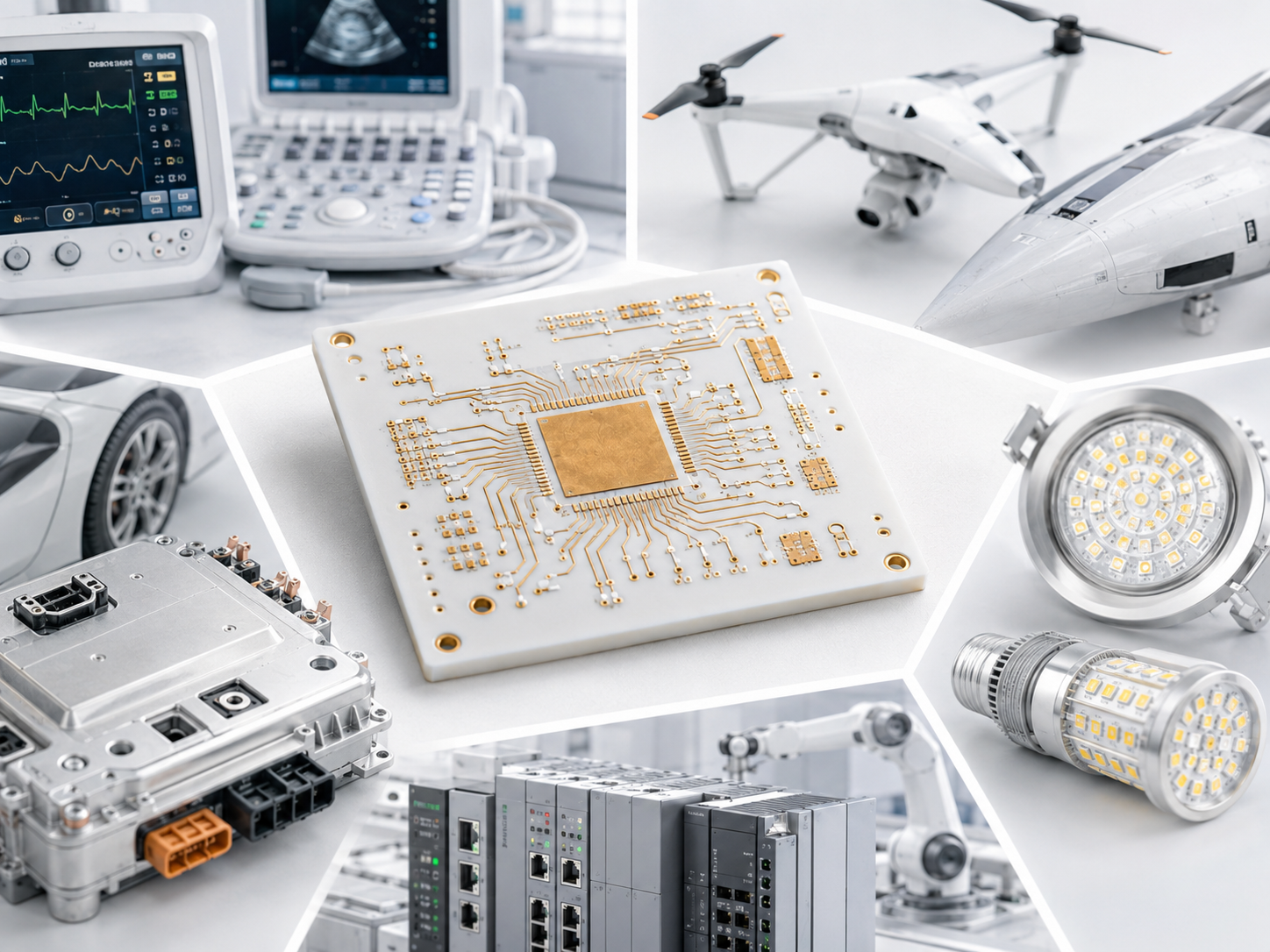
          You may also like