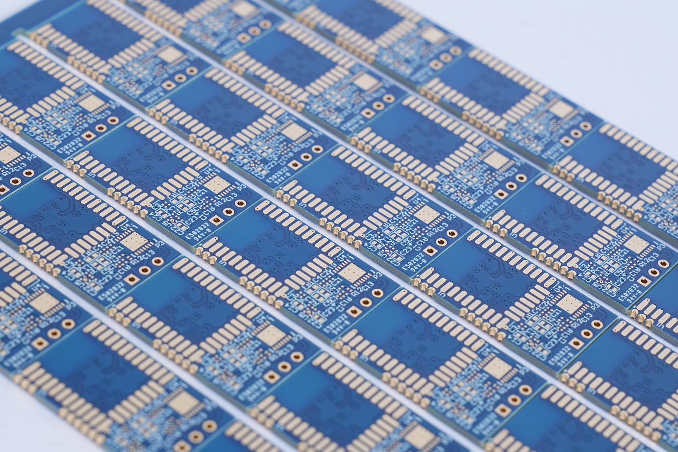
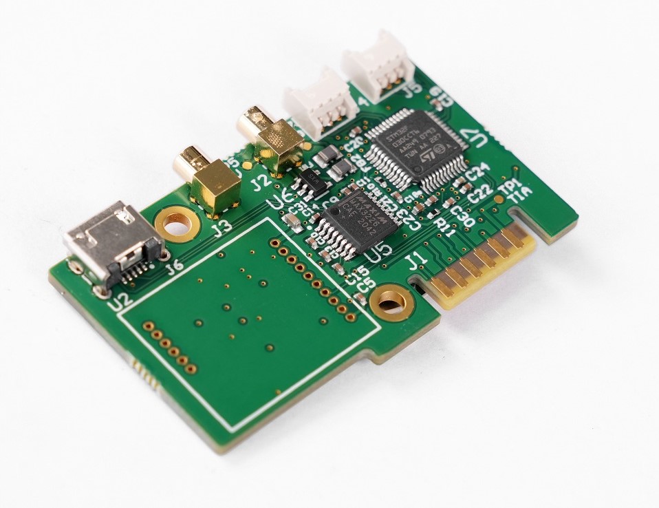
A blank pcb board can mean either raw copper-clad laminate with no circuit pattern or a fabricated PCB with traces and pads but no mounted components. Before buying, identify which state you need, then specify the substrate, copper, thickness, surface finish, fabrication data, and test evidence. Treating every “blank” board as the same product is how buyers end up with material they cannot etch, boards they cannot assemble, or quotations that are impossible to compare.
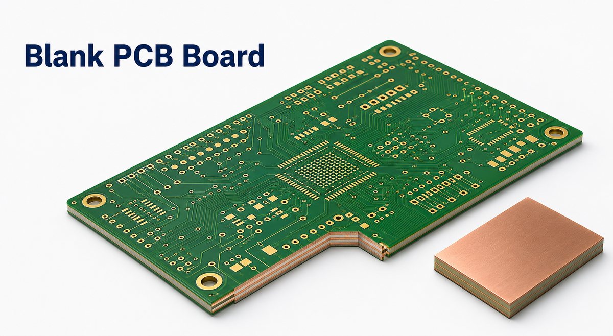
What Is a Blank PCB Board, and What Does “Blank” Actually Mean?
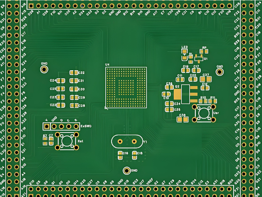
A blank PCB board is a board without mounted electronic components, but the amount of fabrication already completed varies. In an online store, it may be an unpatterned copper-clad sheet. In a fabrication quotation, it usually means a finished bare PCB with designed conductors, holes, solder mask, silkscreen, and exposed pads.
Use more precise language in drawings and purchase orders:
- Copper-clad laminate: insulating substrate bonded to copper, before a circuit image is formed.
- Fabricated bare PCB: the custom circuit pattern is complete, but no components are installed.
- Unpopulated PCB: another practical name for a fabricated board before assembly.
- Prototype board or zero board: a generic perforated board with pads or strips for hand wiring; it is not a custom routed PCB.
- PCBA: a PCB after components have been mounted and soldered.
If you only need a broader terminology overview, the existing BestPCBs article on what a blank PCB is covers the basic definition. For a quote, replace “blank board” with the exact deliverable so the supplier knows whether to price sheet material, bare-board fabrication, or assembly.
How Do Blank PCB Boards Work?
Blank PCB boards do not perform an electronic function by themselves. They provide the insulating base and conductive structure needed to build a circuit, and the way they are used depends on how much of that structure is already present.
- Raw copper-clad laminate: the copper must be imaged, etched or milled into isolated conductors before components can be connected.
- Perforated prototype board: fixed pads or copper strips provide connection points, and the circuit is created with component leads and manual wiring.
- Custom fabricated bare PCB: designed traces, pads, vias, holes, and finishes already form the required interconnections, but the board still needs components and assembly before the circuit can operate.
Once components are mounted and soldered, the blank or bare board becomes a PCBA. Its electrical behavior then comes from the combination of the copper network, installed components, power, firmware, and external connections.
Blank Copper PCB Board Options
A blank copper PCB board is normally sold as single-sided or double-sided copper-clad laminate, while a custom fabricated board may contain one, two, or many patterned copper layers. The correct option depends on whether you will create the circuit yourself or send digital fabrication files to a board manufacturer.
| Board State | What Is Already Present | Typical Use |
| Unpatterned single-sided copper clad | Copper on one face of the substrate | Simple DIY etching or milling |
| Unpatterned double-sided copper clad | Copper on both faces | Two-sided experiments and plated-hole development |
| Perforated prototyping board | Repeated pads, holes, or copper strips | Hand-wired circuits and laboratory prototypes |
| Custom fabricated bare PCB | Designed traces, pads, vias, mask, legend, and finish | Prototype or production assembly |
Do not order a raw copper sheet when the assembly team expects finished pads and plated holes. Conversely, a fabricated board is not a reusable blank canvas: its circuit pattern is already fixed by the Gerber or ODB++ data.
How Is a Blank PCB Board Different from a Bare PCB, Zero PCB, and PCBA?
The difference is the board’s manufacturing state, not simply whether it looks empty. “Bare PCB” is the most useful production term for a fabricated board without components, while “zero PCB” or protoboard usually describes a generic board that the user wires manually.
| Term | Circuit Pattern | Components |
| Raw copper-clad blank | No | No |
| Custom bare PCB | Yes | No |
| Zero PCB or protoboard | Generic pads or strips | No |
| PCBA | Yes | Yes |
This distinction also changes the files required. Raw sheet material is ordered by material, dimensions, and copper. A custom bare PCB needs manufacturing data. A PCBA adds a BOM, component placement data, assembly drawings, polarity information, and test requirements.
Blank PCB Material Selection
Blank PCB material should be chosen from the electrical, thermal, mechanical, and assembly requirements—not from color or price alone. Standard FR-4 is a practical starting point for many rigid boards, but it is not automatically suitable for high-frequency, high-temperature, flexible, or heat-spreading applications.
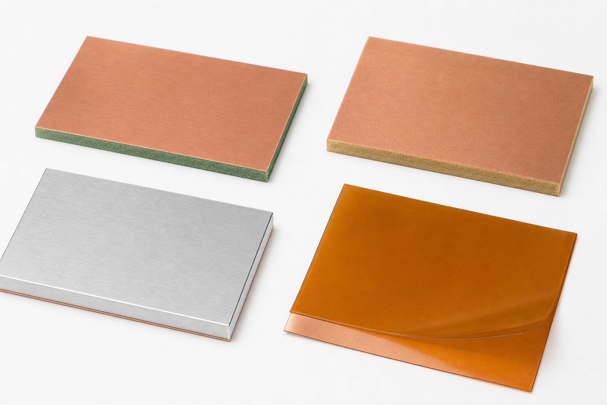
| Material Family | Suitable Starting Point | What to Confirm | Common Misuse |
| FR-4 | Rigid control, consumer, industrial, and general electronic boards | Tg, thickness, copper, dielectric needs, assembly temperature, and end-use environment | Assuming every FR-4 grade has the same thermal and electrical behavior |
| Paper-phenolic or composite laminate | Simple, cost-sensitive, low-complexity products when the construction is acceptable | Mechanical strength, moisture behavior, punching/drilling route, and safety requirements | Substituting it for FR-4 without checking reliability and process compatibility |
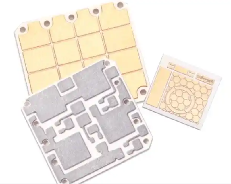
| Low-loss laminate | RF, microwave, antenna, or high-speed designs with controlled dielectric performance | Dk, Df, copper roughness, thickness tolerance, stackup, and approved material | Selecting by brand name without defining the electrical target |
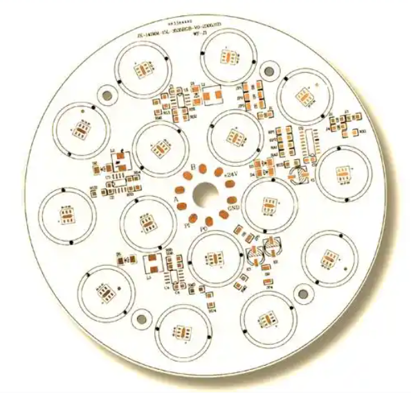
| Aluminum or copper-core material | LED and power designs that need a defined thermal path | Dielectric thermal performance, isolation, base thickness, mounting, and flatness | Treating metal-core material as a substitute for thermal design |
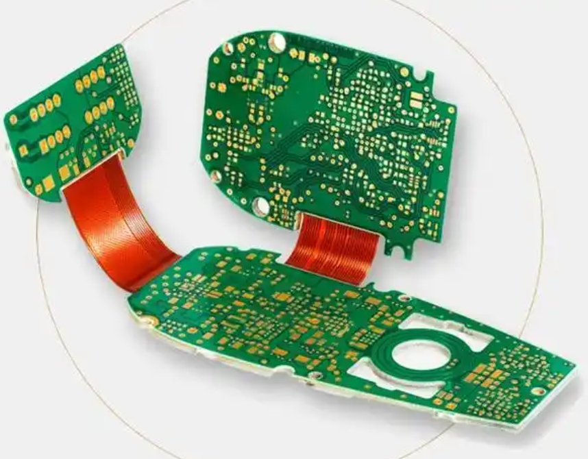
| Polyimide flex material | Bending, folding, lightweight, or space-constrained interconnects | Dynamic versus static flex, bend zone, copper type, coverlay, and stiffeners | Using rigid-board bend assumptions on a flexible circuit |
For a deeper material breakdown, see what circuit boards are made of. In an RFQ, use an approved laminate designation or measurable requirements whenever substitution would affect impedance, thermal cycling, flammability, or product qualification.
Which Copper Weight and Board Thickness Should You Choose?
Choose copper weight from current, heat, trace geometry, voltage spacing, and etching capability; choose board thickness from mechanical support, connector fit, enclosure tolerance, and stackup needs. “Standard” values are useful starting points, not substitutes for design review.
- 0.5 oz copper: can support finer features, but the finished copper condition and plating must be defined.
- 1 oz copper: a common starting point for general rigid boards, subject to current and geometry checks.
- 2 oz or heavier copper: may help power distribution, but it changes etching, spacing, hole plating, thermal balance, and cost.
- 0.8-1.0 mm boards: may suit compact products, but can flex more and need assembly handling review.
- 1.6 mm boards: are widely used as a mechanical starting point, but connector and enclosure requirements still control the choice.
- Thicker constructions: can add stiffness yet may complicate drilling, aspect ratio, press-fit hardware, and depaneling.
State whether copper refers to starting foil or finished copper. For plated outer layers, the final condition may differ from the purchased foil. Also define total board thickness and tolerance rather than allowing the supplier to infer them from an old drawing or a sample.
How to Use Blank PCB Board
How to use blank PCB board depends on whether it is raw copper clad, a prototyping board, or a custom fabricated bare board. Each one starts at a different step, so using the wrong workflow can damage the material or create an unreliable circuit.
For raw copper-clad material:
- Confirm the substrate, copper sides, copper thickness, dimensions, and flatness.
- Create a verified circuit image with adequate clearance, pad size, and drill registration.
- Use a controlled imaging and copper-removal method suitable for the material.
- Drill and profile the board without breathing fiberglass or laminate dust; use local extraction and suitable personal protection.
- Handle etchants and cleaning chemicals according to their safety data sheets and local disposal rules.
- Inspect conductor continuity, isolation, edge damage, residual copper, and pad adhesion before soldering.
For a fabricated bare PCB, do not redesign the circuit on the physical board. Verify the revision, dimensions, holes, finish, solder mask, marking, and electrical-test status, then release it to assembly under controlled storage and handling conditions. A production board should be built from released design data rather than copied from an improvised hand-etched sample.
What Fabrication Features Must Be Defined Before Ordering?
A custom blank board cannot be quoted reliably from the phrase “FR-4, two layers” alone. The supplier needs enough controlled information to reproduce the electrical network, mechanical outline, material construction, protective coatings, and inspection scope.
| Requirement Group | Information to Provide |
| Digital fabrication data | Gerber or ODB++, NC drill files, netlist when available, and revision identification |
| Construction | Layer count, stackup, material, total thickness, copper, impedance, and controlled dielectric notes |
| Mechanical data | Profile, slots, cutouts, edge plating, countersinks, tolerances, panelization, and breakaway method |
| Surface protection | Solder mask, silkscreen, surface finish, peelable mask if used, and special handling areas |
| Quality and delivery | Performance class, electrical test, impedance report, coupons, microsection, marking, packaging, and quantity |
A fabrication drawing should settle requirements that are not unambiguous in the layer data. If a feature is critical to connector fit, creepage, heat transfer, RF behavior, or regulatory testing, call it out explicitly and resolve questions before production release.
Complete the RFQ with prototype and forecast quantities, the required delivery format, packaging needs, and the actual target date. Add a short readme that identifies the authoritative revision, especially when the release contains several data formats. Remove obsolete exports instead of leaving the supplier to decide which file is current. Include a BOM and component placement data only when assembly review or PCBA pricing is also required.
How Are Blank PCB Boards Manufactured?
Fabricated blank PCB boards are made by converting controlled design data into patterned, drilled, plated, protected, finished, and tested boards. The exact route varies with layer count and technology, but the sequence must preserve registration and connectivity from incoming laminate to final inspection.
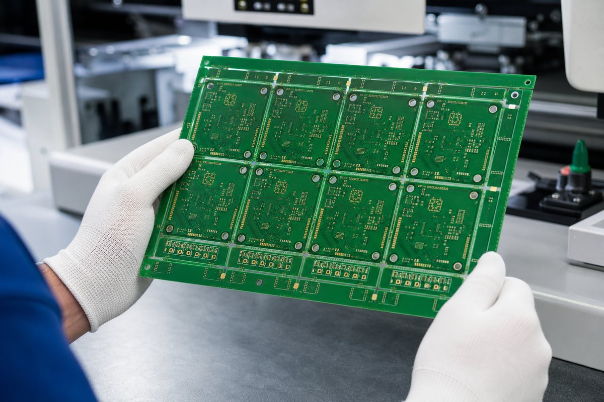
- CAM and DFM review: verify layers, drills, profile, spacing, annular rings, mask openings, panelization, and special notes.
- Material preparation: issue the specified laminate, copper, and prepreg with controlled identity and condition.
- Inner-layer imaging and etching: form inner conductors on multilayer designs and inspect the pattern.
- Lamination: bond cores and prepreg under a controlled cycle for multilayer boards.
- Drilling and copper plating: create mechanical and via holes, then form conductive hole walls where required.
- Outer-layer imaging and etching: build the final external copper pattern.
- Solder mask and legend: protect conductors and add approved identification.
- Surface finish: protect exposed pads and prepare them for the intended assembly process.
- Profiling and depanel features: route, score, or otherwise form the final outline and delivery panel.
- Test and inspection: verify electrical networks and the physical characteristics required by the drawing.
The BestPCBs PCB manufacturing process page provides additional fabrication context. The buyer should still confirm the actual process route against the current design rather than assuming every blank board follows the same controls.
Which Tests Confirm a Blank Board Is Ready for Assembly?
A blank board is ready for assembly only when its electrical networks and relevant physical characteristics meet the released data. Electrical test detects opens and shorts, but it does not replace dimensional, visual, structural, finish, or cleanliness checks.
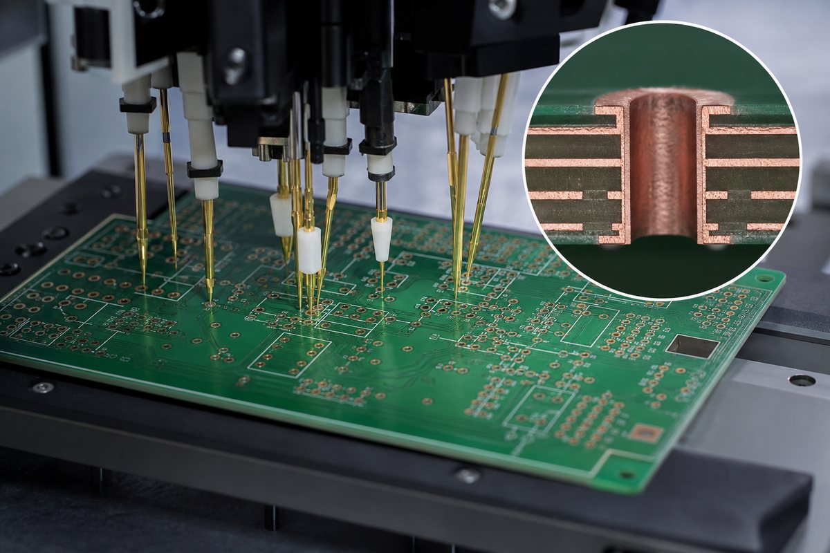
| Check | What It Confirms |
| Electrical test | Continuity and isolation of the intended conductive networks |
| Visual or automated optical inspection | Observable conductor, mask, legend, finish, and surface anomalies |
| Dimensional inspection | Profile, holes, slots, thickness, tooling features, and specified tolerances |
| Microsection evaluation | Selected internal features such as plated hole walls, layer alignment, and laminate condition |
| Impedance verification | Controlled-impedance coupon or trace performance when specified |
| Finish and solderability checks | Condition of assembly surfaces under the agreed inspection or test method |
IPC-9252 addresses electrical testing of unpopulated printed boards. IPC-A-600 provides visual acceptance illustrations, while IPC-6012 defines qualification and performance requirements for rigid printed boards. The applicable revision, class, addenda, deviations, and customer drawing requirements should be agreed in the procurement documents rather than assumed.
What Defects Should Stop a Blank PCB Board from Being Used?
Stop the board before assembly when a defect can affect connectivity, insulation, soldering, mechanical fit, material integrity, or traceability. Mounting components on a questionable bare board adds labor and parts to a defect that was cheaper to contain earlier.
- Open or short circuit: quarantine the affected lot and compare the failure with the netlist and test data.
- Lifted, missing, or damaged copper: do not repair by guesswork where current, impedance, spacing, or long-term adhesion matters.
- Plated-hole or annular-ring anomaly: review breakout, voids, cracks, wall condition, and the applicable acceptance criteria.
- Delamination, blistering, measling, or severe discoloration: investigate material condition and thermal or process exposure.
- Solder mask on a required pad or exposed copper where protection is required: assess assembly and insulation risk before release.
- Oxidized, contaminated, scratched, or uneven finish: confirm whether solderability and storage life have been compromised.
- Incorrect profile, hole, slot, thickness, or excessive bow and twist: stop if the board will not fit the enclosure, fixture, connector, or assembly line.
- Wrong revision or unreadable traceability marking: treat identity loss as a control failure even if the board looks acceptable.
Not every cosmetic variation is a reject, and not every hidden reliability risk is visible. Use the drawing, purchase specification, agreed performance class, and applicable acceptance documents to decide. When the disposition is unclear, hold the material and obtain a documented engineering or quality decision.
Blank PCB Board Price Factors
Blank PCB board price is driven by the board state and manufacturing burden, so a raw copper-clad sheet cannot be compared directly with a tested custom multilayer bare PCB. A useful quotation separates the design-dependent cost drivers instead of presenting one unexplained unit price.
| Cost Driver | Why It Changes the Price |
| Board size and panel utilization | Determine material usage, routing, handling, and boards per production panel |
| Layer count and stackup | Add imaging, lamination, registration, drilling, and process control |
| Material and copper | Special laminates, heavy copper, and tight dielectric requirements change material and process routes |
| Hole and feature complexity | Small holes, high hole count, blind or buried vias, and tight spacing increase processing demand |
| Surface finish and mask requirements | Different finishes and selective requirements change chemistry, control, and inspection |
| Testing and documentation | Electrical test, impedance, coupons, reports, microsections, or special inspection add work |
| Quantity and schedule | Setup cost, panel efficiency, material availability, and expedited routing affect the quote |
Compare each blank PCB board supplier using the same released package and the same assumptions. A lower quotation may exclude electrical testing, use a different laminate, relax tolerances, change the finish, or omit documentation. Clarify those differences before judging total cost.
FAQ About Blank PCB Boards
Is a blank PCB board the same as a bare PCB?
Often, but not always. In PCB fabrication, both terms commonly describe an unpopulated board with a completed circuit pattern. In hobby and retail searches, “blank PCB” can instead mean unpatterned copper-clad laminate. A purchase order should say either “copper-clad laminate” or “fabricated bare PCB” and list what features must already be present.
Can a blank PCB work without electronic components?
A fabricated bare PCB can provide continuity between its designed nodes, but it does not perform the intended electronic function without the required components. It is an interconnection structure, not a finished device. Passive structures such as antennas or test coupons can have measurable behavior on an unpopulated board, but that does not make a typical product PCB operational.
Why is a blank PCB usually green?
The green color normally comes from solder mask, not from the base laminate. Solder mask covers and protects most of the external copper while leaving selected pads exposed for assembly. Other mask colors are available. Color alone does not identify the substrate, copper weight, Tg, layer count, or electrical performance.
Can components be soldered directly to copper-clad laminate?
Not as a controlled custom circuit until conductive features, isolation gaps, pads, and holes have been created. Soldering arbitrary parts to an unpatterned copper surface can create shorts and weak mechanical joints. For a repeatable product, define the layout and fabricate the intended conductor pattern before assembly.
Can you cut a blank PCB board to size?
Raw laminate can be cut with suitable equipment, dust extraction, edge control, and personal protection. A fabricated PCB should be profiled from released mechanical data because cutting after fabrication can damage traces, planes, edge clearances, plating, or controlled geometry. Never assume unused-looking board area contains no internal copper.
Should you choose a single-sided or double-sided copper blank?
Choose single-sided material for a simple circuit that can be routed and assembled on one conductive layer. Choose double-sided material when routing density or grounding requires both sides and when you have a reliable registration and interconnection method. For plated through holes and repeat production, custom fabrication is usually more controlled than a manual DIY process.
What copper thickness is common on a blank PCB?
Half-ounce, one-ounce, and two-ounce copper are common starting points, but the correct value depends on the design and on whether the supplier is describing starting foil or finished copper. Current, heat, spacing, etching, plating, and reliability requirements should drive the selection. Put the copper definition in the stackup or fabrication drawing.
What files are needed for a custom blank PCB?
Provide Gerber or ODB++ data, NC drill files, a fabrication drawing, stackup, material, copper, thickness, surface finish, solder mask, quantity, and test requirements. Add netlist data when available. If you also need assembly, include the BOM, component placement file, assembly drawing, polarity information, and test expectations.
Does every blank PCB need electrical testing?
Electrical-test scope should be agreed for the product, quantity, risk, and procurement requirements. Testing is used to verify continuity and isolation against the design data. It does not confirm every physical attribute, so it should be paired with the necessary visual, dimensional, structural, finish, and documentation checks.
How should unpopulated PCBs be stored?
Keep them clean, dry, protected from abrasion, and sealed in packaging appropriate to the surface finish and expected storage period. Avoid touching exposed pads, mixing revisions, or leaving boards uncovered near chemicals and dust. If packaging has been damaged or storage limits are uncertain, assess surface condition and solderability before assembly.
What is the HS code for a blank printed circuit board?
Customs classification depends on the board’s actual condition, destination, national tariff schedule, and import documentation. A fabricated unpopulated printed circuit may be classified differently from raw copper-clad laminate or an assembled board. Do not copy a code from a search result; verify the current classification with the importer, customs broker, or destination authority.
Is a blank PCB board the same as a breadboard?
No. A solderless breadboard is a reusable prototyping tool with internal spring contacts. A perforated protoboard is soldered and manually wired. A custom bare PCB has a fixed manufactured circuit pattern. They can all support development work, but they differ in electrical behavior, durability, repeatability, and suitability for production.
How Can EBest Circuit Review Your Blank PCB Board Order?
EBest Circuit can review your blank PCB board requirements before quotation. Send your Gerber or ODB++ data, drill files, fabrication drawing, stackup, material, copper weight, board thickness, surface finish, quantity, target delivery date, and test requirements to sales@bestpcbs.com. If the project will later move into assembly, include the BOM and component placement data so our engineering team can review PCB fabrication and PCBA requirements together.