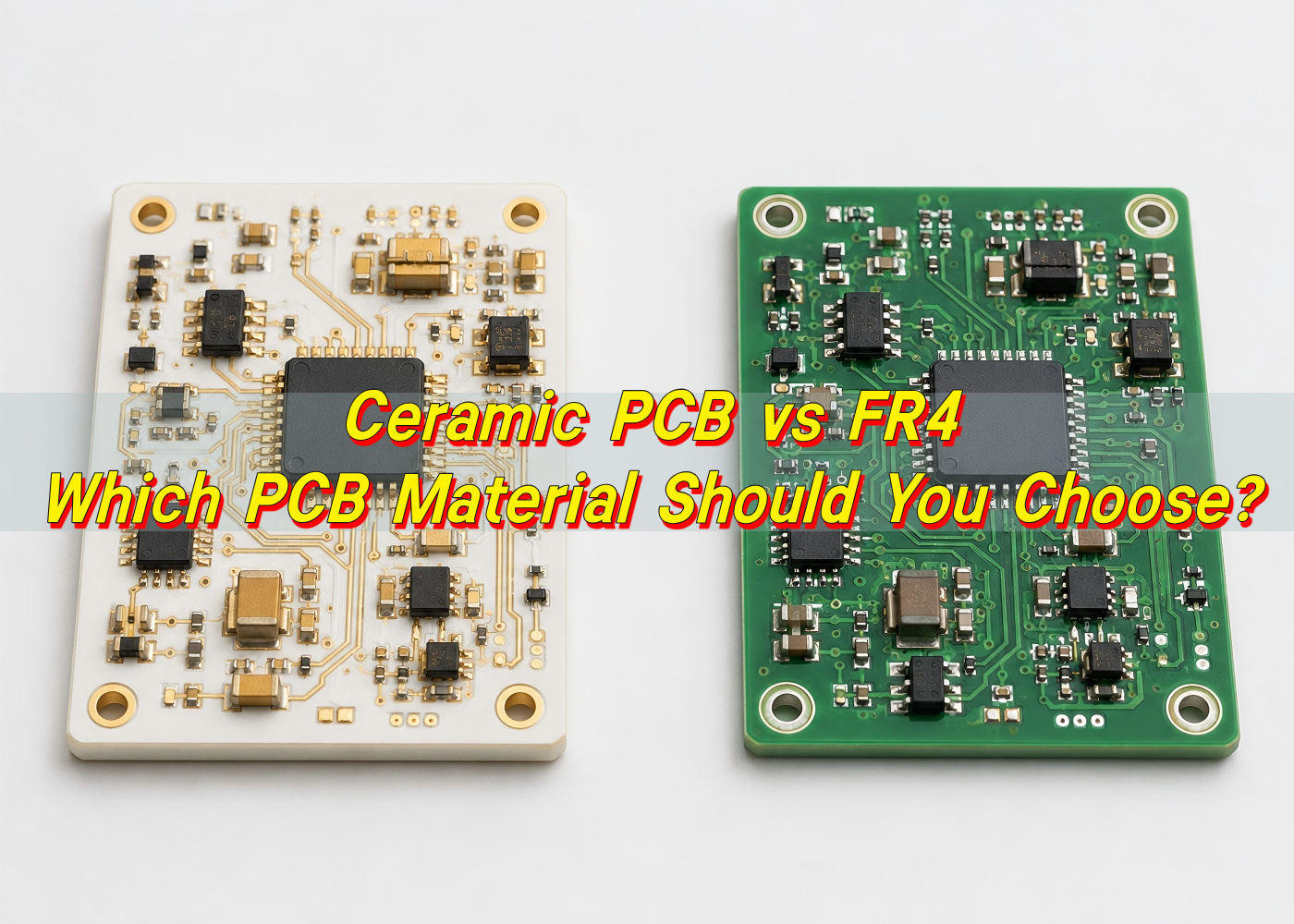
Choosing between ceramic PCB VS FR4 PCB is not only a material decision. It affects heat flow, electrical stability, board thickness, cost, lead time, assembly reliability, and long-term product performance. For many standard electronic products, FR4 is practical, proven, and cost-friendly. For high-power, high-temperature, high-frequency, or high-reliability designs, ceramic PCB can offer a stronger technical foundation.
At EBest Circuit (Best Technology), we usually recommend customers review the application first, not the material name first. Heat, voltage, frequency, size, reliability target, assembly method, and production volume should guide the decision. Once these points are clear, the comparison becomes much easier.
What Is a Ceramic PCB?
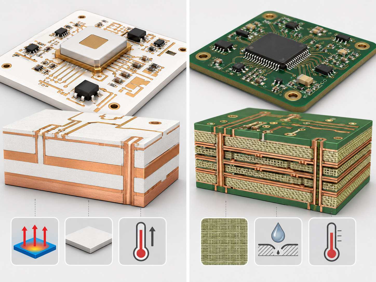
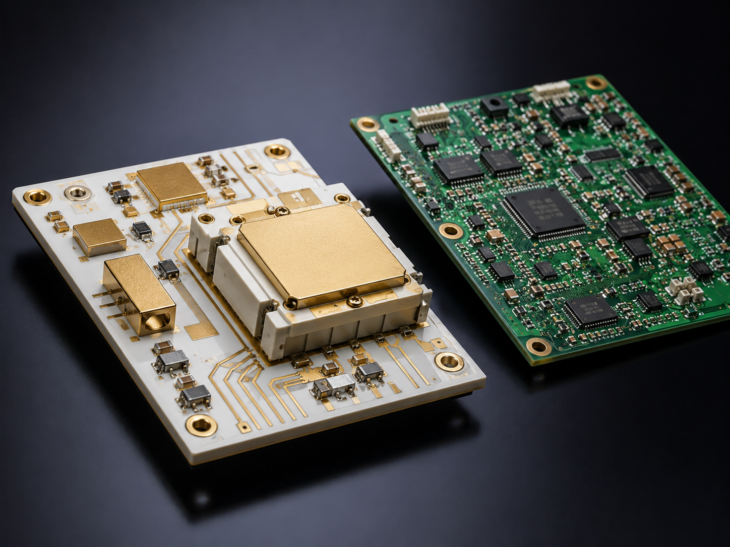
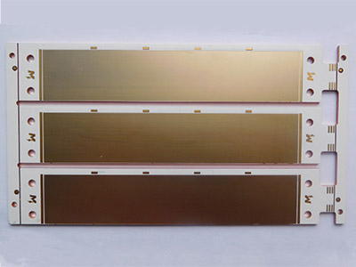
Ceramic PCB is a printed circuit board that uses a ceramic substrate instead of a traditional glass-reinforced epoxy base. The most common ceramic PCB materials include alumina, aluminum nitride, and sometimes silicon nitride. These materials are selected because they provide excellent thermal conductivity, strong electrical insulation, stable mechanical properties, and reliable performance under demanding conditions.
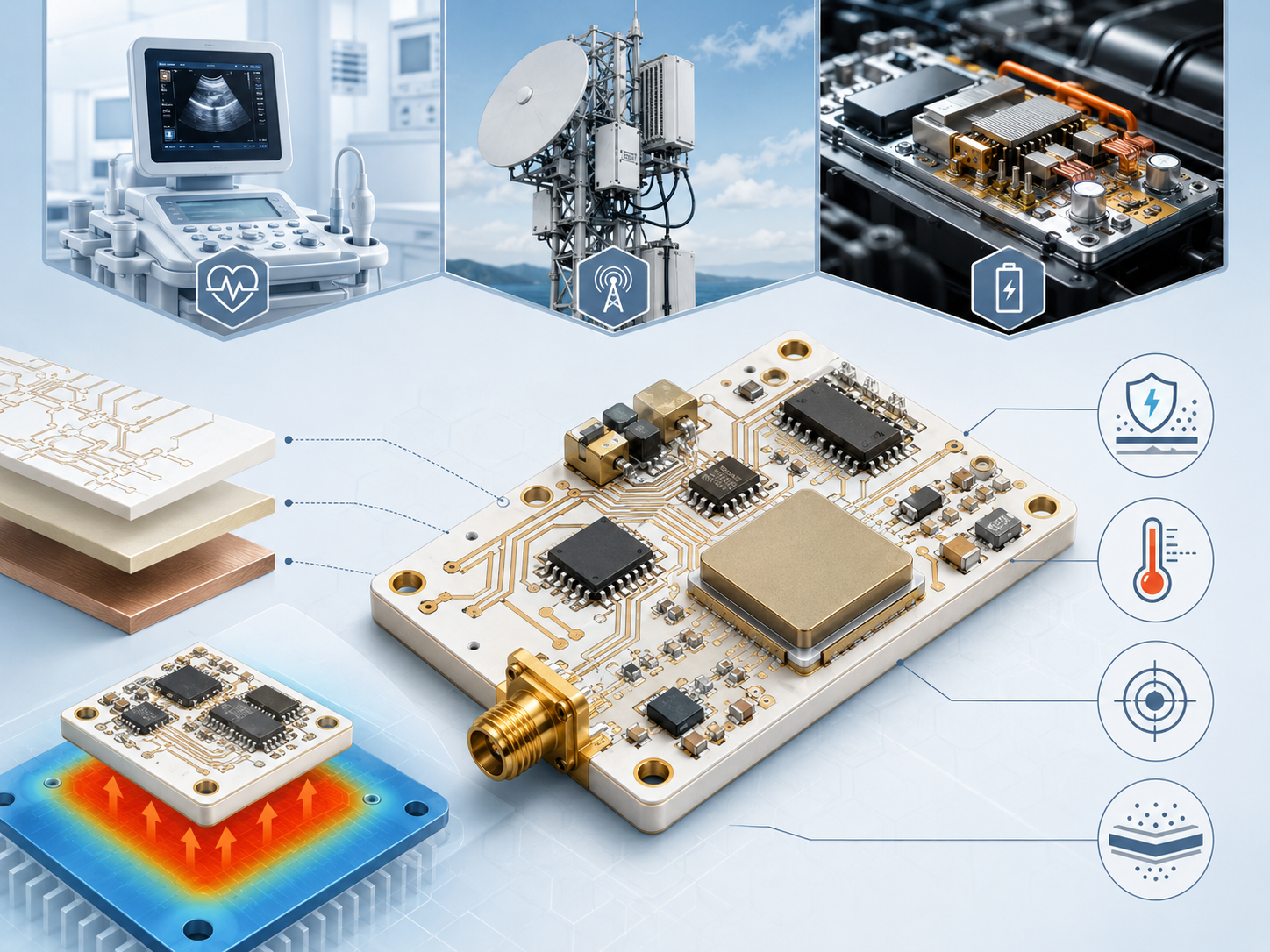
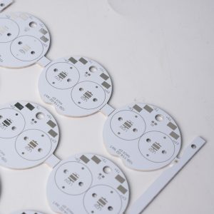
Ceramic PCBs are widely used in high-power LED modules, power electronics, RF circuits, semiconductor packaging, laser systems, medical equipment, sensor modules, and automotive electronics. These applications often need compact layouts and steady performance over long service life.
Common ceramic PCB manufacturing processes include thick film, thin film, direct plated copper, direct bonded copper, and active metal brazing. Each process has its own copper thickness range, bonding strength, line width capability, and cost level. For example, DPC ceramic PCBs are suitable for fine circuits and precision applications, while DBC and AMB ceramic substrates are often used for high-current and power module designs.
A ceramic PCB is often chosen when engineers need:
- Better heat transfer from components to the substrate
- Stable electrical insulation under high voltage or high temperature
- Good dimensional stability for precision circuits
- Long service life in harsh environments
- Compact packaging for high-density power or RF designs
What Is an FR4 PCB?
An FR4 PCB is the most widely used type of printed circuit board in the electronics industry. FR4 refers to a glass fiber reinforced epoxy laminate. It acts as the insulating base material that supports copper circuits, solder mask, silkscreen, plated holes, and electronic components.
FR4 became popular because it offers a strong balance of performance, availability, manufacturability, and cost. It is easy to process, suitable for single-sided, double-sided, and multilayer boards, and compatible with most standard PCB fabrication and PCBA assembly workflows.
The key strength of FR4 is its versatility. It can support simple low-cost boards and advanced multilayer designs. Designers can select different Tg grades, copper weights, thicknesses, and finishes based on the application. High-Tg FR4 materials are also available for products that require better thermal resistance during soldering and operation.
FR4 PCB is commonly used for:
- Control boards
- Consumer electronics
- Industrial automation circuits
- Power supply control sections
- Communication modules
- IoT and smart devices
- General LED driver boards
- Automotive signal and control electronics
FR4 is a dependable choice when the board does not need extreme thermal conductivity from the base material. It can still handle many thermal designs through copper thickness, thermal vias, heat sinks, metal enclosures, and proper layout strategy. For many projects, this makes FR4 the most practical starting point.
Ceramic PCB vs FR4: What Is the Main Difference?
The main difference between ceramic PCB and FR4 PCB is the substrate material. Ceramic PCB uses a ceramic base with higher thermal conductivity, better dimensional stability, and stronger high-temperature performance. FR4 PCB uses glass fiber epoxy laminate, which is easier to manufacture, more flexible in multilayer design, and more cost-effective for general electronics.
A clear comparison helps explain the practical difference:
| Comparison Item | Ceramic PCB | FR4 PCB |
|---|---|---|
| Base material | Alumina, aluminum nitride, silicon nitride, or other ceramic substrate | Glass fiber reinforced epoxy laminate |
| Main strength | Thermal conductivity, insulation, stability, reliability | Cost efficiency, routing flexibility, broad availability |
| Typical thermal conductivity | Much higher, depending on ceramic material | Lower, usually around standard epoxy laminate levels |
| High-temperature behavior | Excellent stability in demanding environments | Good for standard electronics, improved with high-Tg material |
| Mechanical behavior | Hard and dimensionally stable | Strong, process-friendly, and more forgiving |
| Multilayer routing | Available, but process depends on ceramic technology | Very mature and widely used |
| Fine circuit capability | Strong with DPC or thin-film process | Strong with HDI and advanced FR4 fabrication |
| Cost level | Higher | Lower |
| Best fit | Power, RF, LED, medical, automotive, aerospace, high-heat modules | General electronics, control boards, digital circuits, cost-sensitive products |
In everyday engineering terms, FR4 is the reliable workhorse, while ceramic PCB is the performance-focused material for tougher electrical and thermal requirements. A well-designed FR4 board can serve many products beautifully. A ceramic board becomes valuable when ordinary thermal paths or insulation strategies are no longer enough.
EBest Circuit often helps customers review this point during DFM evaluation. Sometimes a customer asks for ceramic PCB because they believe it is always better. After checking the power, thermal path, size, and cost target, FR4 may be enough.
How Does Ceramic PCB vs FR4 Compare in Thermal Conductivity?
Thermal conductivity is one of the most important reasons engineers compare ceramic PCB vs FR4. Ceramic substrates conduct heat much better than standard FR4 materials. This allows heat generated by LEDs, power semiconductors, RF devices, and high-current components to move more efficiently through the board.
Here is a practical comparison:
| Material Type | Typical Thermal Conductivity Range | Practical Meaning |
|---|---|---|
| Standard FR4 | Around 0.3 W/m·K | Suitable for general electronics with moderate heat |
| High-performance FR4 variants | Higher than standard FR4, but still limited compared with ceramics | Useful when better thermal resistance is needed without changing board family |
| Alumina ceramic PCB | Commonly around 20–30 W/m·K | Strong option for LED, sensors, power modules, and stable insulation |
| Aluminum nitride ceramic PCB | Commonly around 150–180 W/m·K or higher depending on grade | Excellent choice for high-power and high-heat-density applications |
| Silicon nitride ceramic PCB | Strong thermal and mechanical performance depending on grade | Suitable for advanced power modules and demanding environments |
Thermal conductivity should be considered together with copper thickness, component package, solder layer, interface material, enclosure design, and airflow. A material with high conductivity can still perform poorly if the heat path is interrupted.
For LED lighting, ceramic PCB can help maintain lower junction temperature, which supports brightness stability and product life. For power electronics, it helps spread heat from MOSFETs, IGBTs, power diodes, and driver ICs. For RF circuits, stable temperature can also support more consistent electrical behavior.
In a practical design review, EBest Circuit usually checks heat source position, copper area, substrate thickness, via design, soldering process, and expected operating temperature. This prevents overpaying for materials in simple projects and helps select stronger substrates for products that require high thermal endurance.
Is Ceramic PCB Better Than FR4 for High-Power Applications?
Ceramic PCB is often better than FR4 for high-power applications because it provides a more efficient path for heat dissipation and offers excellent electrical insulation. High-power electronics create concentrated heat. If that heat stays near the component, it can affect output stability, solder joint reliability, and long-term product performance. Ceramic material helps move that heat away more effectively.
High-power applications where ceramic PCB is often considered include:
- High-power LED modules
- Laser diode modules
- Power semiconductor substrates
- EV power electronics
- Industrial motor control modules
- RF power amplifiers
- Medical power devices
- Aerospace and defense electronic modules
- Compact DC-DC converters
- High-voltage sensor and insulation circuits
Ceramic also performs well in applications where high voltage and heat appear together. Many ceramic substrates provide high dielectric strength, low moisture absorption, and stable insulation performance. These features are valuable for power modules that must operate safely and consistently over time.
FR4 remains widely used in power electronics as well. Many power supplies, inverters, chargers, and control boards use FR4 successfully. The key is that FR4 often needs additional thermal design support. This may include heavier copper, thermal vias, heat sinks, insulated metal substrates, or mechanical heat spreaders.
A useful way to decide is to review the heat path. If the main heat path depends on the PCB base material, ceramic is worth serious consideration. If the heat can be handled by copper, airflow, housing, or external heat sinks, FR4 may keep the project more cost-efficient.
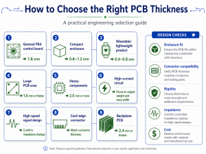
When Should You Choose an FR4 PCB?
You should choose an FR4 PCB when your project needs a proven, economical, and flexible board material for general electronic functions. FR4 is especially suitable for signal routing, digital circuits, control boards, moderate-power applications, and products where cost control matters.
FR4 is a strong choice when your design has these characteristics:
- The circuit is mainly digital, analog, control, or mixed-signal.
- Heat generation is moderate and manageable through layout.
- The project needs multilayer routing.
- The budget requires efficient material cost.
- The board needs common PCB processes such as plated through holes, impedance control, solder mask, and standard surface finish.
- The product does not require extreme thermal conductivity from the substrate.
- The design needs quick prototyping and easy scaling to production.
Here is a simple guide:
| Project Requirement | Is FR4 a Good Choice? | Reason |
|---|---|---|
| Low to medium heat | Yes | Thermal needs can usually be handled by layout and copper design |
| Complex multilayer routing | Yes | FR4 multilayer fabrication is highly mature |
| Cost-sensitive production | Yes | Material and processing costs are efficient |
| General control electronics | Yes | FR4 supports stable, reliable circuit performance |
| Very high heat density | Depends | Additional thermal structures may be needed |
| High-power LED chip directly on board | Sometimes, but ceramic or metal core may perform better | Heat path becomes more critical |
| RF or microwave circuit | Depends | Special RF laminates or ceramic may be needed for tighter performance |
When customers contact EBest Circuit for a new PCB project, FR4 is often the first material we evaluate because it is practical and widely suitable. If the design review shows that FR4 can meet the electrical, thermal, and mechanical requirements, it often provides the best cost-performance ratio.
When Should You Choose a Ceramic PCB?
You should choose a ceramic PCB when your design needs high thermal conductivity, strong insulation, compact heat management, high-frequency stability, or long-term reliability in demanding environments. Ceramic is especially valuable when performance stability matters more than material cost.
Ceramic PCB is a strong choice when the project has these needs:
- High heat generation from LEDs, power chips, laser diodes, or RF devices
- Compact board size with limited heat-spreading area
- Strong electrical insulation under high voltage
- Stable dielectric properties for high-frequency circuits
- High reliability under thermal cycling
- Low moisture absorption for sensitive applications
- Good dimensional stability for precision assembly
- Longer service life in industrial, medical, automotive, or aerospace products
The type of ceramic also matters. Alumina is popular because it balances performance and cost. Aluminum nitride is preferred when thermal conductivity is the main priority. Silicon nitride can support applications that need strong mechanical reliability and thermal performance. The circuit process also matters because DPC, DBC, AMB, thick film, and thin film ceramic boards serve different design goals.
A practical selection table can help:
| Application Need | Suitable Ceramic Option | Why It Helps |
|---|---|---|
| Balanced thermal performance and cost | Alumina ceramic PCB | Reliable, widely used, stable, and cost-effective among ceramics |
| Very high thermal conductivity | Aluminum nitride ceramic PCB | Excellent heat transfer for dense power designs |
| High-current power module | DBC or AMB ceramic substrate | Strong copper bonding and power handling |
| Fine lines and precision circuits | DPC or thin-film ceramic PCB | Supports accurate circuit features |
| Harsh working environment | Alumina, AlN, or Si3N4 depending on design | Stable insulation and thermal performance |
EBest Circuit (Best Technology) supports ceramic PCB material selection, DFM review, prototype production, and PCBA assembly support.
Ceramic vs PCB: Is Ceramic a PCB Material or a PCB Type?
Ceramic is a PCB material, and a ceramic PCB is a PCB type that uses ceramic as its substrate. Because PCB refers to the finished printed circuit board, while ceramic refers to the base material used to build a certain kind of PCB.
Think of PCB as the general product category. Inside that category, there are many material and structure options. FR4 PCB, ceramic PCB, aluminum PCB, copper core PCB, rigid-flex PCB, and high-frequency PCB are all different forms of printed circuit boards.
Here is a simple explanation:
| Term | Meaning | Example |
|---|---|---|
| PCB | Printed circuit board used to connect and support components | Any electronic circuit board |
| FR4 PCB | PCB made with FR4 glass epoxy laminate | Control board, IoT board, industrial PCB |
| Ceramic PCB | PCB made with ceramic substrate | LED module, power substrate, RF module |
| Ceramic material | The substrate material used in ceramic PCB | Alumina, aluminum nitride, silicon nitride |
| PCB type | A board category based on structure or material | FR4, ceramic, metal core, rigid-flex |
This distinction matters because the design process still follows PCB principles. Engineers still need Gerber files, copper layers, pads, spacing, surface finish, soldering requirements, and testing plans. The difference is that ceramic substrates require specific manufacturing methods and design rules. Hole processing, edge treatment, copper bonding, and metallization are different from standard FR4 fabrication.
Which PCB Material Is Better for LED, Power, and RF Applications?
The better PCB material depends on the application. For standard LED driver boards, FR4 may be suitable. For high-power LED modules where heat must move quickly from the light source, ceramic PCB or metal core PCB is often stronger. For power electronics, FR4 works well in control sections, while ceramic is preferred for dense power substrates. For RF circuits, material choice depends on frequency, dielectric stability, loss, and thermal needs.
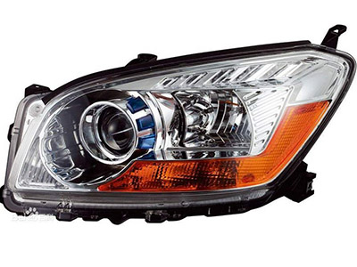
For LED applications, ceramic PCB is attractive when the LED package produces high heat in a small area. Ceramic helps move heat away from the LED, which can support stable brightness and longer product life. FR4 can still be used in LED driver circuits, control boards, and lower-power lighting products.
For power applications, ceramic PCB performs well when the substrate must provide both insulation and heat transfer. This is common in power modules, high-voltage circuits, and compact converters. FR4 is still widely used for power supply control boards, gate driver boards, and general power electronics where the thermal design can be handled with copper, vias, and external heat sinks.
For RF applications, ceramic can provide stable dielectric properties and good thermal behavior, especially in compact or high-power RF modules. However, many RF PCBs also use specialized laminates such as Rogers materials, PTFE-based materials, or hydrocarbon ceramic-filled laminates.
| Application | FR4 PCB | Ceramic PCB | Practical Recommendation |
|---|---|---|---|
| Low-power LED control board | Very suitable | Usually more than needed | FR4 is often practical |
| High-power LED module | Possible with careful thermal design | Very suitable | Ceramic or metal core PCB is often preferred |
| LED driver circuit | Very suitable | Selected for special thermal or insulation needs | FR4 is common |
| Power control board | Very suitable | Used when heat or insulation requirements are high | Choose based on heat density |
| Power module substrate | Limited in high heat density modules | Excellent | Ceramic is often stronger |
| RF low-frequency circuit | Suitable in many cases | Sometimes selected | FR4 may work if requirements are moderate |
| RF high-power or high-stability circuit | Depends on frequency and loss limits | Strong option | Ceramic or RF laminate may be better |
| Medical or aerospace high-reliability electronics | Suitable for many control circuits | Strong for thermal and stable substrate needs | Review reliability target carefully |
The strongest material choice is usually application-specific. A product can also use more than one PCB type. For example, a power device may use an FR4 control board and a ceramic power substrate in the same assembly. EBest Circuit supports PCB fabrication and PCBA assembly for different material categories, including FR4, metal core PCB, ceramic PCB, RF PCB, and high-reliability boards.
Why Is Ceramic PCB More Expensive Than FR4 PCB?
Ceramic PCB is more expensive than FR4 PCB because the raw material, manufacturing process, metallization method, processing difficulty, and inspection requirements are more demanding. Ceramic substrates are harder and more brittle than FR4 laminates, so cutting, drilling, edge processing, copper bonding, and surface preparation require specialized control.
FR4 manufacturing is extremely mature and widely scaled. Material supply is broad, production lines are optimized, and standard processes can produce large volumes efficiently. Ceramic PCB production is more specialized. The factory must control substrate quality, metallization adhesion, copper thickness, dimensional tolerance, and thermal reliability with greater precision.
The cost difference comes from several main factors:
| Cost Factor | Ceramic PCB | FR4 PCB |
|---|---|---|
| Raw material | Higher-cost ceramic substrates | Cost-efficient laminate materials |
| Processing method | Specialized laser, mechanical, metallization, or bonding processes | Mature drilling, plating, imaging, etching, and lamination |
| Copper bonding | Requires ceramic-compatible metallization or direct bonding | Standard copper-clad laminate process |
| Tooling and handling | More careful handling due to hardness and brittleness | More forgiving in standard fabrication |
| Yield control | Requires tight control for cracks, adhesion, and flatness | Highly standardized yield management |
| Application requirements | Often used in high-reliability products | Used across broad commercial and industrial products |
| Production scale | More specialized volumes | Large global production scale |
Ceramic PCB cost also depends on material type. Alumina is usually more economical than aluminum nitride. Aluminum nitride offers much higher thermal conductivity, so it carries a higher material cost. The circuit process also changes pricing. DPC, DBC, AMB, thick film, and thin film processes have different cost structures.
Board size, copper thickness, line width, spacing, hole design, surface finish, tolerance, and inspection level also affect price. A simple alumina ceramic PCB may be relatively manageable in cost. A high-power AMB substrate or fine-line DPC ceramic board may require a higher budget because it delivers more advanced performance.
EBest Circuit (Best Technology) can support material selection, DFM review, PCB fabrication, component sourcing, PCBA assembly, and testing for projects moving from prototype to production. For engineers comparing FR4 vs ceramic, our team can review your Gerber files, stackup, power conditions, and reliability targets before recommending the most suitable board solution.
For project review or quotation support, contact EBest Circuit (Best Technology) at sales@bestpcbs.com.


")

")