PCB manufacturing PCB manufacturing
Home > Blog

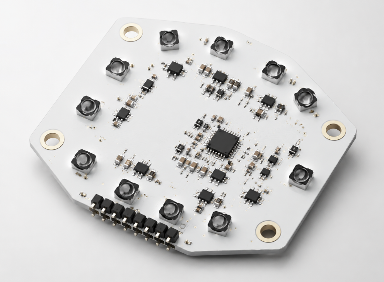
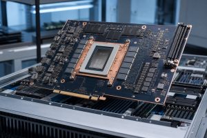
Machine Vision Board Design & Manufacturing for Industrial Image Processing

August 13th, 2026

A machine vision board must acquire every required frame, preserve trigger timing, process the image within the cycle time, and deliver a valid result under sustained industrial load. That outcome depends on the complete path: camera interface, FPGA/GPU/NPU partitioning, DDR buffering, PCIe or network transfer, power, heat, PCB construction, assembly, and functional test.

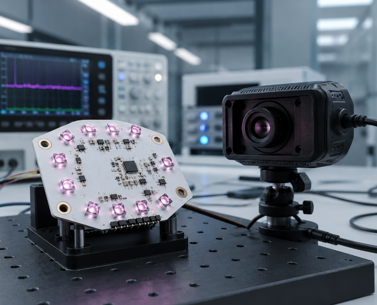
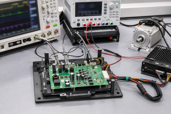
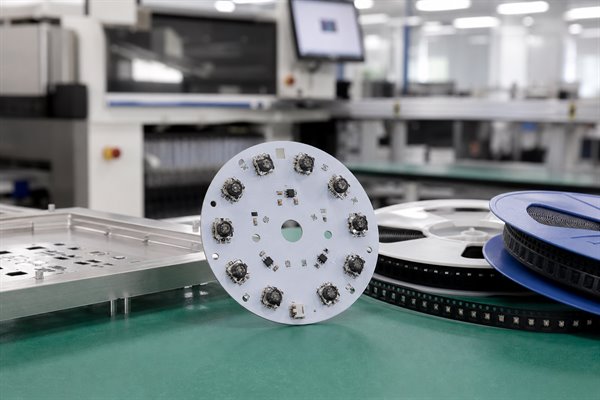
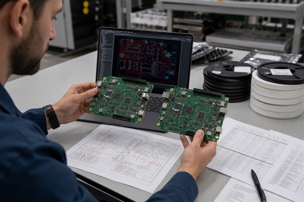
Machine vision board design beside an industrial camera and optical inspection equipment

What Is a Machine Vision Board for Industrial Image Processing?

A machine vision board is the deterministic hardware path between image capture and a machine decision. It accepts one or more camera streams, associates frames with triggers or timestamps, performs preprocessing or inference, and sends results to a host, PLC, robot controller, or motion system.

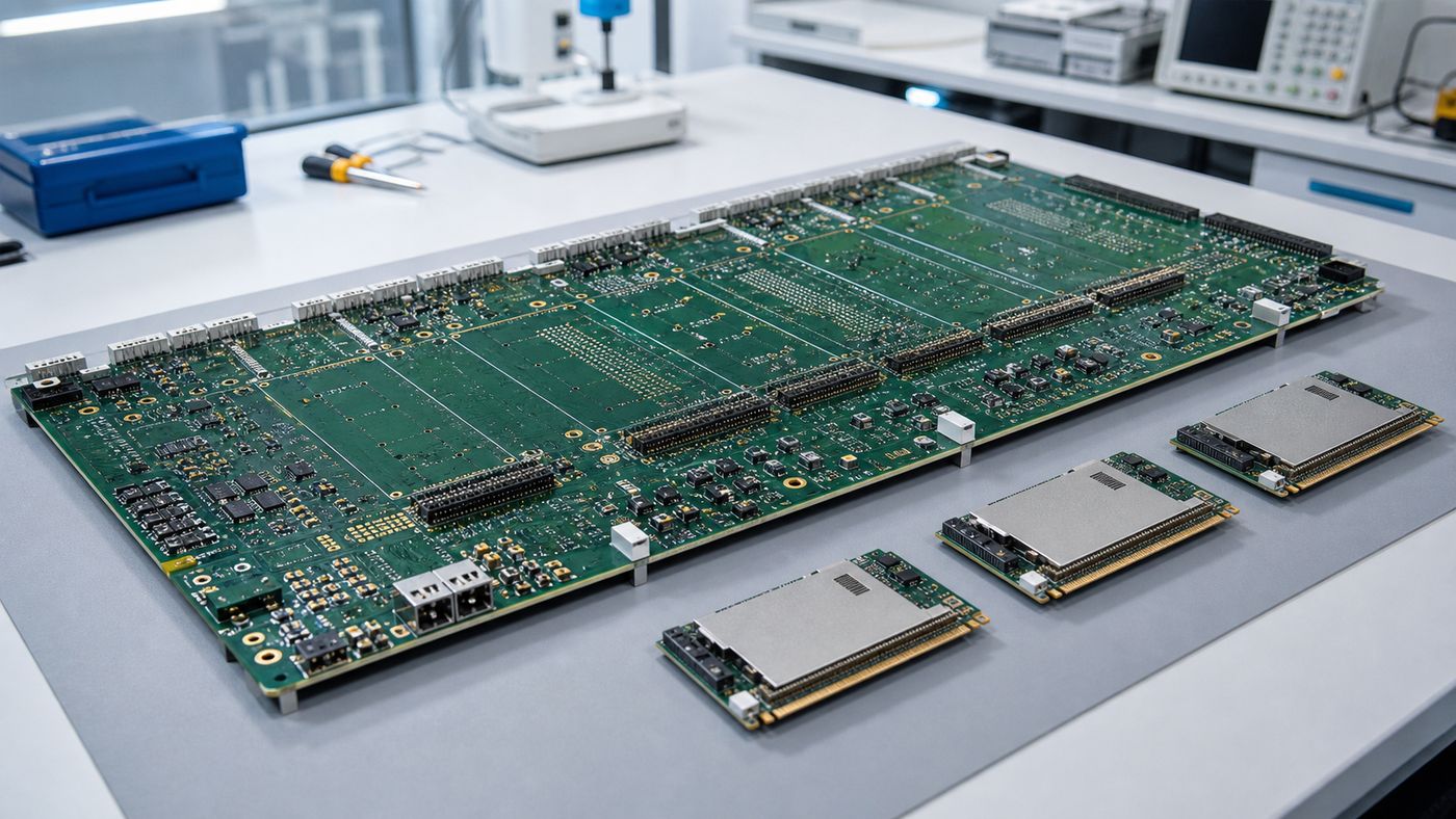
The board may be a PCIe frame grabber, an embedded controller, or a custom PCBA inside an inspection machine. Its functional boundary is wider than a camera PCB module, which mainly supports the sensor and local imaging electronics, and different from an IP camera PCB, which is organized around network video capture and delivery. A machine vision board commonly owns frame buffering, deterministic I/O, image processing, diagnostics, and host communication.

For AOI, robotic guidance, metrology, sorting, and multi-camera inspection, image quality is only one acceptance item. The specification must also define maximum trigger-to-result latency, permitted camera skew, dropped-frame behavior, recovery time, operating temperature, output safety state, and the exact revision of firmware and AI models used for acceptance.

How Should You Choose FPGA, GPU, or NPU Processing for a Machine Vision Board?

Select compute by assigning each pipeline stage to the device that can meet its worst-case latency, throughput, power, and software-support requirement. Peak TOPS does not prove that a board can ingest every camera, move intermediate data through memory, and return a decision before the machine cycle expires.

Processing option Best use Board design impact
FPGA Sensor control, protocol conversion, line-rate filtering, pixel alignment, and deterministic trigger logic Multiple clock domains, high-speed I/O banks, configuration memory, timing closure, and tightly sequenced rails
GPU Flexible image algorithms, large parallel workloads, and models that change during product development High DDR traffic, substantial core power, heat spreading, and dependency on drivers and software libraries
NPU Supported neural-network inference where performance per watt is the main constraint Operator and precision compatibility, model conversion, accelerator memory movement, and fallback planning
Hybrid FPGA acquisition and preprocessing followed by GPU or NPU analytics Explicit buffer ownership, inter-device bandwidth, timestamp transfer, boot order, and error recovery

FPGA-based image processing is useful when parallel, data-heavy front-end operations must run with stable latency. A practical hybrid design can perform debayering, region extraction, line buffering, or geometric correction in FPGA logic and send only the required frames or features to a GPU or NPU. This reduces downstream traffic, but it also creates a new verification boundary: the design must prove how metadata, timestamps, frame IDs, and error flags move with the processed data.

Before fixing the processor, benchmark the intended pipeline with the actual resolution, bit depth, camera count, model, precision mode, and temperature target. Record average and worst-case latency, memory usage, accelerator utilization, and throttling behavior. If a required AI operator is unsupported, model conversion changes accuracy, or performance collapses after thermal saturation, the board architecture is not ready for release.

Which Camera Interfaces Belong on an Industrial Machine Vision Board?

Use MIPI CSI-2 for nearby embedded sensors, GigE Vision for distributed industrial cameras, and USB3 Vision for high-throughput host-connected cameras where cable routing and service access are controlled. The choice must follow physical placement, sustained payload, synchronization method, connector life, field replacement, and the software ecosystem.

Interface Suitable architecture PCB priority Acceptance focus
MIPI CSI-2 Image sensor mounted on the same assembly or connected through a short controlled interconnect Continuous reference planes, controlled differential geometry, short lane transitions, and correct sensor rail sequencing Lane mapping, bit depth, frame start/end integrity, clock behavior, and error counters
GigE Vision Remote or distributed cameras that benefit from Ethernet infrastructure and field-serviceable cabling PHY and magnetics placement, return-path isolation, connector shielding, surge/ESD strategy, and network power planning when applicable Sustained packet delivery, timestamp behavior, packet loss, recovery, and multi-camera traffic contention
USB3 Vision High-data-rate cameras located near the host or embedded controller SuperSpeed channel loss, connector footprint, ESD parasitics, power integrity, and cable retention Enumeration, sustained transfer, reconnect recovery, host-controller loading, and dropped-frame counters

Do not treat a common software layer as proof that the electrical links are interchangeable. Each interface needs its own impedance plan, connector model, protection components, power budget, compliance test, and error-injection method. If one board supports several camera types, isolate their clock and bandwidth domains and define which device owns triggers, timestamps, buffers, and recovery.

How Do Pixel Rate, DDR Bandwidth, and PCIe Traffic Shape the Board Architecture?

Calculate sustained traffic separately for camera input, every DDR read/write pass, accelerator transfer, and host output. The basic raw payload is active width x active height x frame rate x bits per pixel x camera count. Add protocol, alignment, blanking, metadata, and retry allowances only after the raw stream is visible.

As an illustrative calculation, a 1920 x 1080 stream at 60 frames per second and 10 bits per pixel carries 1,244,160,000 raw bits per second, or 155.52 MB/s before overhead. Four such cameras produce 622.08 MB/s. If the pipeline writes raw frames to DDR, reads them for processing, writes an intermediate result, reads it again for inference, and sends the output to a host, total memory traffic can be several times the incoming payload.

Industrial image data path from camera acquisition through FPGA GPU or NPU processing and DDR buffering to system output

Build a bandwidth worksheet with one row for each transfer, its direction, payload, burst size, duty cycle, and simultaneous operating condition. Size DDR from the sum of competing reads and writes, not the camera stream alone. Size frame buffers from the longest permitted backpressure or recovery interval, then define what happens when the buffer fills: block acquisition, drop the newest frame, drop the oldest frame, or flag the inspection cycle invalid.

PCIe lane rate is not application payload. Encoding, packets, transaction size, DMA descriptors, cache behavior, host contention, and software scheduling reduce usable throughput. The acceptance test should therefore measure sustained end-to-end traffic with all cameras active and retain margin for bursts, temperature-related throttling, error recovery, and future firmware growth.

What PCB Layout Risks Threaten High-Speed Image Data Integrity?

The dominant risks are discontinuities in impedance and return current, not simply long traces. A nominally matched differential pair can still fail at a connector breakout, layer transition, via stub, split reference plane, oversized ESD pad, or noisy receiver reference.

  • Lock the stack-up: obtain the fabricator’s dielectric thicknesses, copper weights, material family, and impedance geometry before high-speed placement is frozen.
  • Preserve return paths: keep each lane over a continuous reference plane and place nearby return vias when signals change reference layers.
  • Control transitions: include connector fields, AC-coupling pads, ESD devices, test points, and BGA escape vias in the channel model.
  • Separate noise sources: keep switch nodes, motor or strobe currents, high-current connector returns, and fast clocks away from camera analog rails and sensitive references.
  • Verify the real channel: use the transmitter, receiver, connector, via, and material models required by the component vendors; do not apply one universal length or skew limit to every interface.

Dense FPGA, processor, or DDR fan-out may require an HDI PCB structure, but microvias cannot correct a poor topology. Review via-in-pad requirements, capture-pad size, sequential lamination, escape layers, reference changes, and inspection access together. Where margin is limited, run pre-layout and post-layout signal-integrity checks against the actual stack-up.

How Should Power Integrity, Heat, and Mechanical Constraints Be Reviewed?

Power, thermal, and mechanical reviews must use the same worst-case operating mode because rail droop, throttling, and board strain can produce identical intermittent image faults. Create a rail budget for every processor, FPGA bank, DDR rail, camera supply, PHY, illumination control, and auxiliary I/O.

  • Define rail behavior: record nominal voltage, tolerance, steady current, transient current, sequencing, soft-start, reset relationship, monitoring, and shutdown state.
  • Design the PDN: select bulk and high-frequency decoupling from the device impedance target and package model, then check plane spreading and via inductance.
  • Test sustained heat: run the maximum camera count and processing load until temperatures stabilize; observe junction estimates, regulator temperatures, clock reduction, and frame latency.
  • Close mechanical clearances: check heat-sink attachment, connector mating space, cable bend and retention, mounting-hole stress, enclosure airflow, and probe access.

A thermal solution is acceptable only if the board meets timing and image-throughput limits at the specified enclosure temperature. Likewise, a mechanical drawing is incomplete if it omits connector keep-outs, camera harness direction, heat-sink loading, or the tolerance stack between the PCB, standoffs, enclosure, and optical assembly.

How Is a Machine Vision Board Manufactured and Assembled?

Manufacturing should begin with a stack-up and assembly-risk review tied to the exact board revision. High-speed routing, fine-pitch BGA escape, blind or buried vias, heavy connectors, and thermal pads affect fabrication, solder-paste design, inspection, rework, and test-fixture access.

The following values come from EBest Circuit’s current English FR-4 capability workbook. General values are starting points for review; special-process values require confirmation against the final stack-up, panel, copper distribution, via structure, and reliability requirements.

  • FR-4 layer count: the general capability is 1-10 layers, with high-Tg material required for 8 layers and above. Designs from 10-32 layers require special-process review.
  • Laser blind or buried vias: the general capability is 0.10 mm. The final review must confirm capture pads, via fill, and the sequential-lamination structure.
  • Minimum finished hole: the general capability is 0.20 mm. A 0.15 mm finished hole requires special-process review.
  • Through-hole aspect ratio: the general capability is 8:1. A ratio up to 10:1 requires special-process review.
  • 1 oz line and space: the general capability for inner or outer layers is 4/4 mil. A 3/3 mil design requires special-process review.
  • ENIG thickness: the listed range is 0.025-0.125 um for gold and 3-8 um for nickel. Wear, contact, or bonding requirements must be confirmed separately.

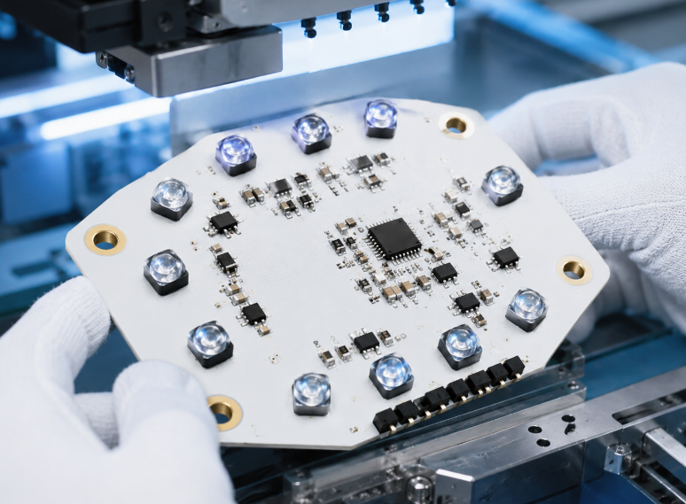
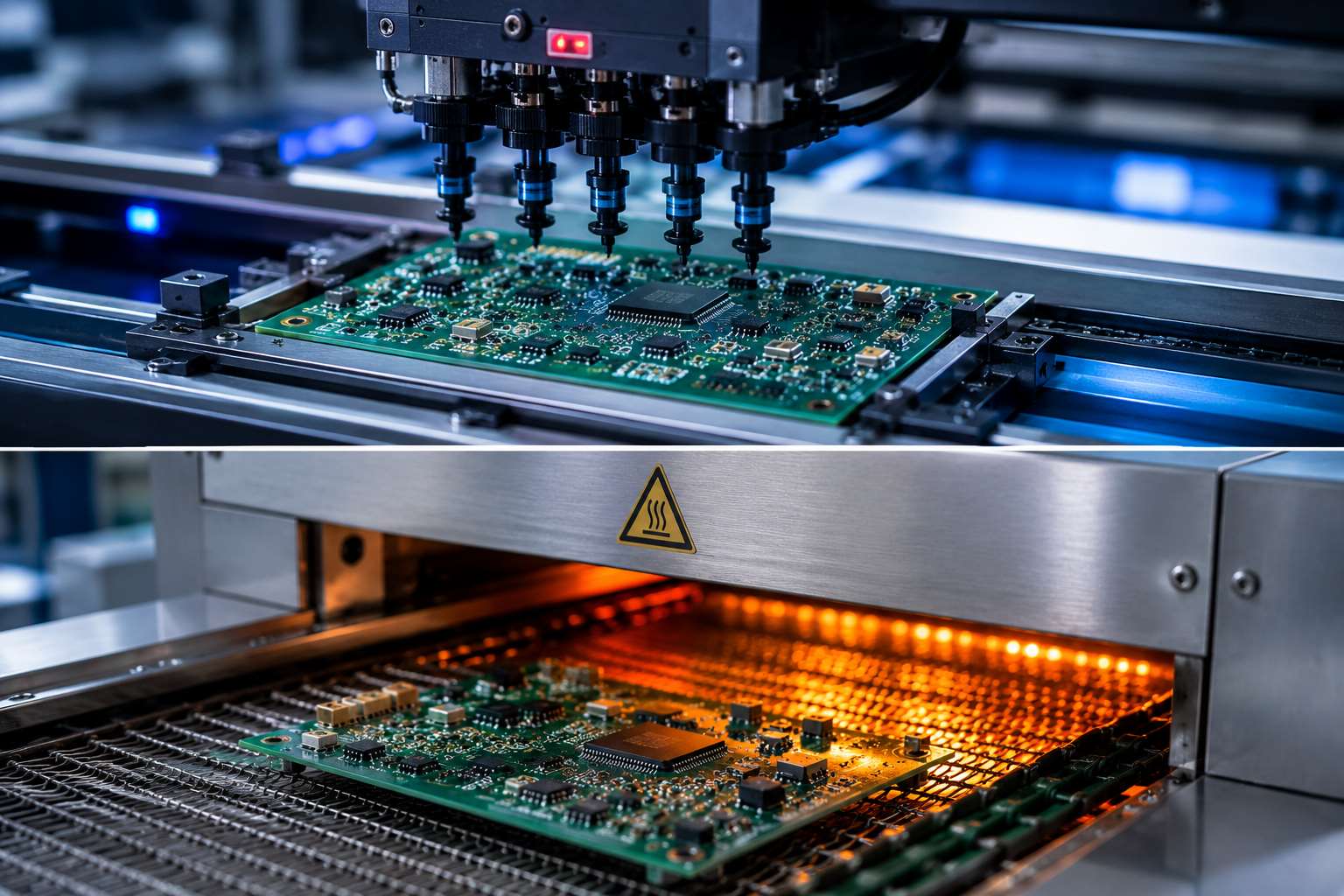
Before assembly, classify bottom-terminated components, fine-pitch BGAs, large exposed pads, moisture-sensitive packages, press-fit parts, high-mass connectors, and devices that require programming. Paste apertures and reflow profiling should address voiding and thermal imbalance without creating solder starvation. AOI verifies visible placement, polarity, and joints; X-ray supports hidden-joint inspection. Neither replaces electrical and functional testing of the image path.

How Should Trigger, Synchronization, and Functional Testing Be Validated?

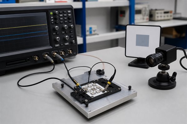
Validation must correlate the commanded trigger, actual frame, hardware timestamp, processed result, and system output under sustained load. A live image proves only that part of the path is operating; it does not prove that the correct frame belongs to the correct machine event.

Machine vision board trigger synchronization and functional testing loop
  • Verify power and boot: test cold starts, warm restarts, brownouts, and maximum-load transitions. Record rail timing, reset release, clocks, boot logs, and current profiles; boot loops, unstable links, corrupted configuration, or abnormal current are failures.
  • Confirm image acquisition: run known camera patterns through every supported format, bit depth, and lane configuration. Check frame IDs, line length, pixel order, and link-error counters for lane swaps, truncation, corrupted lines, color errors, or missing frames.
  • Measure trigger and synchronization: apply timed trigger and encoder patterns while all required cameras are active. Compare trigger-to-exposure latency, inter-camera skew, hardware timestamps, and missed-event counts; drifting skew, duplicate events, lost triggers, or incorrect frame association must fail.
  • Stress sustained processing: operate at the maximum camera count, frame rate, algorithm load, and host-transfer rate until temperature stabilizes. Monitor latency distribution, buffer level, DMA counters, temperature, and throttling; backlog growth, dropped frames, timeouts, or stale results show insufficient margin.
  • Challenge fault recovery: introduce controlled cable interruptions, invalid packets, camera resets, and host restarts. Verify the reported error, safe output state, recovery time, restored counters, and log record; silent corruption, unsafe outputs, mixed frame IDs, or manual-only recovery are unacceptable.
  • Control production testing: use a fixture that generates repeatable inputs and reads machine-verifiable outputs. Lock firmware and model versions, camera or pattern-generator settings, instrument setup, numeric limits, timeout rules, and failure codes, then retain results by unit serial number. Golden samples can monitor fixture stability but do not replace calibrated limits and revision control.

What DFM Checks Are Required Before Machine Vision Board Production?

A release-ready DFM review closes fabrication, assembly, test, and configuration risks against one controlled data package. The output should be an issue list with an owner, disposition, affected revision, and evidence that the approved change reached the final files.

  • Stack-up and impedance: confirm material family, finished thickness, copper weights, controlled structures, coupons, and tolerance assumptions.
  • Drill and via plan: check finished holes, aspect ratios, blind/buried-via spans, via fill, backdrill when required, annular rings, and sequential lamination.
  • Assembly access: review paste apertures, thermal pads, polarity, component spacing, rework access, support tooling, press-fit loads, and selective-solder constraints.
  • Mechanical closure: match the PCB outline, connector mating direction, keep-outs, mounting holes, heat sink, enclosure, and cable drawings.
  • Test coverage: provide accessible points for rails, resets, clocks, trigger I/O, programming, debug, boundary scan, and functional fixtures.
  • Configuration control: freeze manufacturer part numbers, approved substitutes, firmware, FPGA images, AI models, programming instructions, and acceptance limits by revision.

The production package should include Gerber or ODB++, drill and stack-up data, schematic PDF, BOM, centroid data, assembly drawings, impedance requirements, mechanical files, programming files, and test instructions. Missing information should remain an open issue; it should not be replaced with an assumed factory default.

Why Choose EBest Circuit for Machine Vision Board Manufacturing?

Choose EBest Circuit to turn a complex machine vision board design into a clearer, lower-risk manufacturing release. Instead of treating fabrication, assembly, component sourcing, programming, and testing as separate activities, the review connects them around the camera-to-result data path that your equipment must sustain.

  • Find production risks earlier: high-speed stack-up, BGA escape, DDR and PCIe routing, thermal pads, connector loads, and test access can be reviewed before tooling and component purchasing make changes more costly.
  • Reduce avoidable revision cycles: fabrication data, BOM, placement files, mechanical constraints, firmware, and acceptance limits are checked as one controlled package, helping prevent mismatched revisions and missing production instructions.
  • Protect schedule and sourcing decisions: special-process features and component constraints are identified for engineering confirmation before they become late quotation, material, assembly, or test surprises.
  • Make quality requirements measurable: camera formats, frame rates, trigger timing, operating temperature, programming steps, and functional limits can be translated into inspection and test requirements for the finished PCBA.

Send your Gerber or ODB++, schematic, BOM, stack-up target, impedance requirements, assembly files, camera specifications, firmware, and test limits. EBest Circuit can use that package to prepare a more relevant manufacturing review and quotation for your machine vision board, with special-process items clearly identified for confirmation.

FAQs About Machine Vision Boards

Q1: What Does a Frame Grabber Do in a Machine Vision System?

A1: A frame grabber receives camera data and presents complete, identified frames to a host or processing pipeline. Depending on the design, it can also control triggers, buffer bursts, convert formats, timestamp events, and move data through DMA.

Q2: How Does Machine Vision Work in an Industrial Inspection System?

A2: Repeatable optics, timing, and part presentation are required while the system controls lighting and exposure, acquires an image, applies a defined inspection pipeline, and sends a result to the machine controller.

Q3: Are FPGAs Still Relevant to Industrial Machine Vision?

A3: Yes, particularly for deterministic acquisition and parallel preprocessing. An FPGA is optional when another device can meet every interface, latency, trigger, power, and software requirement without it.

Q4: What Are Hardware Timestamps Used for in Machine Vision?

A4: Hardware timestamps correlate frames, triggers, encoders, lighting pulses, and motion in a defined clock domain without relying solely on nondeterministic software time.

Q5: What Causes Dropped Frames in a Machine Vision Pipeline?

A5: Frame IDs, buffer levels, timestamps, and boundary-specific error counters locate the failing stage. Causes can include signal errors, insufficient buffers, blocked DMA, host contention, trigger faults, or thermal throttling.

Q6: What Does AOI Test on an Assembled Machine Vision PCB?

A6: AOI checks visible component presence, polarity, placement, and accessible solder joints. It does not verify hidden BGA joints or functional image processing, so X-ray, electrical test, and functional test address different risks.

Q7: What Does PCB Functional Testing Verify?

A7: Functional testing applies controlled inputs and checks defined electrical and system outputs. For a vision board, it can cover boot, rails, clocks, acquisition, memory traffic, host transfer, trigger timing, error reporting, and recovery.

Q8: What Types of Machine Vision Systems Use Custom Processing Boards?

A8: Custom boards suit systems with requirements that commercial hardware cannot meet. Compare form factor, interface mix, latency, environmental limits, machine I/O, development, certification, fixture, lifecycle, and maintenance costs.

Q9: What Are the Main Stages of Machine Vision Processing?

A9: The main stages are acquisition, preprocessing, feature extraction or inference, decision logic, and result communication. Buffering, timestamps, diagnostics, and recovery keep those stages traceable during production use.

Q10: Is Machine Vision the Same as Artificial Intelligence?

A10: No. Machine vision is the complete industrial imaging system, while AI is one possible processing method. Many inspection tasks use geometry, filtering, matching, measurement, or deterministic rules without a neural network.

Conclusion

A reliable machine vision board is specified and verified as one data, timing, power, thermal, manufacturing, and test system. Interface speed or accelerator performance alone cannot guarantee deterministic inspection. The board must sustain every active stream, preserve frame identity, control triggers, tolerate real operating temperature, and produce observable pass/fail evidence.

To request a machine vision board review, email sales@bestpcbs.com with Gerber or ODB++, schematic, BOM, quantity, stack-up and impedance requirements, assembly files, camera formats, bandwidth calculations, trigger specification, mechanical constraints, firmware or programming files, and functional-test limits.

You may also like

Impedance Control PCB: Requirements, Stackup, and Testing

August 13th, 2026

An impedance control PCB can fail even when its Gerber files look correct. A changed dielectric thickness, an unclear reference plane, or an unapproved trace-width adjustment can move the finished impedance outside the required range. The result may be reflections, timing errors, excessive noise, or an interface that works in a prototype but fails after production changes.

The safest approach is to define the electrical target and manufacturing evidence before fabrication begins. This guide explains what customers should release, what a PCB manufacturer should confirm, and how stackup review, test coupons, and time-domain reflectometry (TDR) reports reduce avoidable production risk.

impedance control pcb
Impedance-controlled PCB fabrication connects the approved stackup with measurable production evidence.

What Is an Impedance Control PCB?

An impedance control PCB has one or more transmission lines manufactured to meet specified characteristic-impedance targets. Common examples include single-ended traces and differential pairs used for high-speed digital, communication, or RF signals.

Impedance is affected by the complete trace environment, not trace width alone. Important variables include:

  • Finished trace width and copper thickness
  • Spacing within a differential pair
  • Distance from the trace to its reference plane
  • Dielectric material, thickness, and design Dk
  • Solder mask and nearby copper geometry
  • Etching and lamination tolerances

A calculator can estimate a starting geometry, but the fabricated result depends on the manufacturer’s actual materials and processes. The released design should therefore identify the required impedance, tolerance, signal layers, reference layers, and controlled nets. The PCB supplier can then compare those requirements with the proposed production stackup.

The customer remains responsible for circuit function, interface requirements, signal-integrity targets, and final design approval. EBest Circuit (Best Technology) can review the released files for PCB manufacturability, coordinate a production stackup, fabricate the boards, and provide agreed impedance-testing evidence.

When Does a PCB Need Impedance Control?

Not every signal trace needs controlled impedance. The decision depends on signal edge rate, interconnection length, interface requirements, acceptable reflection, and the complete electrical path. Clock frequency alone is not enough to make the decision.

Customers should evaluate impedance control when a board includes high-speed digital interfaces, RF paths, fast clock or memory signals, antenna feeds, or other transmission lines whose reflections could reduce operating margin. The applicable component and interface specifications should define the required targets.

Skipping control to reduce board cost can create a larger loss later. Possible consequences include:

  • Prototype-to-production performance changes
  • Intermittent communication errors
  • Reduced eye opening or timing margin
  • Excessive ringing, overshoot, or radiated noise
  • Repeated layout changes without proof that fabrication was the cause

The practical decision is not simply “high-speed board or ordinary board.” Identify which nets require control, the target for each net group, and the evidence needed for acceptance. Do not mark every trace as controlled when only a small number of critical nets require it; unnecessary requirements can increase engineering work, coupon space, testing, and cost.

PCB Impedance Control Requirements

An RFQ that says only “impedance control required” leaves essential decisions unresolved. Before quotation or engineering release, provide a controlled-impedance table or equivalent fabrication note that connects each target to specific layers and net classes.

The release package should state:

  • Target impedance for every controlled net class
  • Whether each target is single-ended or differential
  • Required tolerance, such as the project-approved percentage or ohmic range
  • Signal layer and reference plane for each structure
  • Controlled net names or an unambiguous net-class identifier
  • Intended finished copper weight or thickness
  • Approved material family and any required Dk basis
  • Finished board thickness and stackup constraints
  • Whether impedance coupons and TDR reports are required
  • Whether the manufacturer may adjust trace width or spacing

The Gerber or ODB++ data, fabrication drawing, stackup table, net information, and impedance notes must agree. If one file specifies a 100-ohm differential pair while another calls for 90 ohms, fabrication should stop for clarification rather than rely on an assumption.

Customers should also define the approval path. For example, can the PCB manufacturer compensate a finished trace width to suit its etching process? Can it propose a different prepreg while maintaining the approved dielectric thickness and impedance? Which changes require written customer approval? Resolving these questions before CAM release helps prevent untracked changes and repeated quotation cycles.

Controlled Impedance PCB Layer Stackup

The layer stackup connects the electrical model to the material that will be laminated. A nominal layer count and overall thickness are not enough. The manufacturer needs the copper distribution, core and prepreg construction, finished dielectric thicknesses, material data, and reference-plane relationships.

For each controlled structure, confirm:

  • Whether it is a surface microstrip, embedded microstrip, stripline, or coplanar structure
  • Which plane provides the continuous reference
  • The finished dielectric thickness between the signal and reference layers
  • The finished trace width, copper thickness, and differential spacing
  • Whether solder mask is included in the calculation
  • The material Dk value and frequency basis used for modelling
  • Whether nearby copper, plane openings, or routing transitions disturb the structure

A standard stackup can shorten engineering time, but it should not be accepted only because its layer count and board thickness match the design. The available trace geometry must also fit the customer’s routing density and manufacturing limits.

The customer should review the supplier’s proposed production stackup before fabrication. If the supplier changes dielectric thickness or material construction, the calculated line geometry may also need to change. Keep the approved stackup, impedance table, and revised production files under the same revision so purchasing, engineering, and quality teams evaluate one controlled release.

impedance control pcb
CAM and stackup review align controlled traces with available materials and production geometry.

Impedance Control in PCB Manufacturing

Manufacturing converts the approved model into actual copper and dielectric geometry. Lamination, material variation, copper plating, imaging, and etching all influence the finished result. That is why a theoretical value from the design stage cannot, by itself, prove production conformity.

During engineering review, the PCB manufacturer should compare the customer’s targets with the proposed stackup and process capability. If compensation is necessary, the supplier should return the proposed production geometry for approval instead of silently changing controlled features.

Typical manufacturing controls include:

  • Material and stackup verification before lamination
  • CAM checks for controlled nets, reference planes, and coupon structures
  • Process compensation based on the supplier’s qualified etching data
  • Finished-copper and geometry control
  • Coupon fabrication on the same production panel under representative conditions
  • TDR measurement against the agreed target and tolerance
  • Traceable reporting linked to the job, lot, or panel as agreed

Coupon placement and design should represent the relevant production structures. A coupon is useful only when its layer, reference plane, geometry, materials, and processing are representative of the controlled traces being accepted.

If a measured coupon is outside the specified tolerance, the correct response depends on the agreed acceptance plan. The manufacturer should contain the affected material, review the stackup and process data, and communicate the finding before shipment. The customer should decide whether further investigation, rework, rebuild, or a documented deviation is acceptable.

impedance control pcb
A representative impedance coupon can be measured by TDR against the approved target and tolerance.

How to Check Impedance on PCB?

The most common production method is TDR testing of an impedance coupon. The instrument sends a fast electrical transition into the test structure and evaluates reflections along the transmission path. The result is compared with the approved target and tolerance.

Before accepting a test report, check that it identifies:

  • Customer part number and revision
  • Manufacturing job, lot, or panel reference
  • Coupon or test-structure identification
  • Controlled structure and target impedance
  • Required tolerance or acceptance limits
  • Measured result for each reported structure
  • Test date, equipment, or method when required by the quality plan
  • Clear pass/fail status and authorized review

A report showing only one impedance number without identifying the structure or job may not be sufficient for traceability. Likewise, a passing coupon does not prove the performance of the complete assembled product. It demonstrates that the representative PCB structure met the agreed impedance acceptance criteria.

Customers with stricter reliability or compliance needs should define the sampling plan, report format, retention period, and any coupon-storage requirement in the purchase documentation. If direct board measurements, network analysis, or product-level signal-integrity testing are needed, those requirements should be specified separately because they are not automatically included in standard coupon testing.

A Practical Impedance Control PCB Example

Consider a multilayer control board containing a high-speed differential interface and several single-ended clock lines. The initial RFQ includes Gerber files and an overall board thickness, but it does not identify the controlled nets, reference planes, tolerance, or required report.

If fabrication begins from that package, different suppliers may choose different dielectric constructions and compensate the traces differently. The boards may all match the visible artwork while producing different impedance results.

A safer release would include:

  • A table listing each controlled net class and target
  • The approved layer and reference-plane assignments
  • A preliminary stackup with material and thickness constraints
  • Permission boundaries for trace-width or spacing adjustment
  • A requirement for representative coupons and a TDR report
  • A named customer approver for stackup or geometry changes

EBest Circuit (Best Technology) can review this package against available PCB materials and fabrication rules. If the proposed stackup requires a geometry adjustment, the revised values can be returned for customer approval before production. After fabrication, the agreed coupon results can be supplied with the manufacturing record.

This process does not transfer circuit-design ownership to the manufacturer. It gives both parties a controlled handoff: the customer defines the electrical requirement, the manufacturer defines how the approved requirement will be produced and verified, and unresolved differences are closed before material is committed.

FAQs About Impedance Control PCB

Does every high-speed PCB require impedance control? Not automatically. The customer should evaluate signal edge rate, interconnection length, interface specifications, and acceptable reflection. Control the nets whose transmission-line behaviour can affect performance.

What impedance tolerance should I specify? Use the tolerance required by the interface, design analysis, and product acceptance plan. Confirm that the selected PCB construction and supplier process can support it before release; do not assume one tolerance fits every design.

Can a PCB manufacturer change controlled trace width? Only within the agreed approval process. Manufacturing compensation may be necessary, but the proposed finished geometry and stackup should be reviewed when the change could affect routing, clearance, coupling, or signal performance.

Does a passing TDR coupon guarantee that the assembled product will work? No. It verifies the representative PCB structure against the agreed impedance criteria. Component models, connectors, vias, layout transitions, assembly, firmware, and system conditions still affect final performance.

What should I send for an impedance control PCB quotation? Send the fabrication data, drawing, stackup constraints, controlled-net table, impedance targets and tolerances, material requirements, finished thickness and copper requirements, coupon/report expectations, quantity, and revision. For a manufacturing review or quotation, contact sales@bestpcbs.com.

You may also like

Automated X Ray Inspection PCB: What Buyers Should Specify

August 13th, 2026

Automated x ray inspection pcb helps buyers find hidden solder-joint risks that visual inspection or automated optical inspection cannot see beneath BGA, QFN, LGA, and other bottom-terminated packages.

However, simply requesting “X-ray inspection” does not define the inspection coverage, acceptance criteria, records, or response to a failed result. This guide explains what buyers should specify when automated X-ray inspection is part of a PCB assembly quality plan.

automated x ray inspection pcb
Automated X-ray inspection checks hidden PCB assembly joints without damaging the board.

How Does Automated X Ray Inspection PCB Production Work?

An AXI system directs X-rays through an assembled circuit board and records how different materials absorb the radiation. Dense materials, including solder and copper, produce different grayscale patterns from laminate, component bodies, and air gaps.

Inspection software then evaluates selected regions against programmed criteria. Depending on the equipment and inspection plan, the system may check solder-joint shape, void area, ball alignment, bridging, missing connections, or barrel fill.

A repeatable automated sequence includes:

  • Identify the board or production program.
  • Align the PCB using fiducials or programmed reference points.
  • Capture images of selected components and solder joints.
  • Apply predefined inspection algorithms.
  • Classify results as acceptable, defective, or requiring review.

  • Store inspection images and result data when traceability is required.
  • Route a suspected assembly for verification or rework.

Automation improves consistency and throughput, but it does not remove engineering judgment. The inspection program, image quality, component geometry, acceptance limits, and review process still determine whether the result is useful.

Before placing an order, buyers should identify the critical packages, required inspection coverage, applicable workmanship criteria, and evidence expected with the shipment.

When Should Buyers Require Automated X Ray Inspection?

Not every component on every PCBA requires X-ray inspection. Visible components may be inspected effectively with AOI, while electrical and functional tests evaluate different risks.

AXI becomes more valuable when solder joints cannot be seen directly or when a hidden defect could create expensive rework or field failure.

Common reasons to require AXI include:

  • BGA, micro-BGA, CSP, LGA, or bottom-terminated components
  • QFN or DFN packages with thermal pads
  • Package-on-package assemblies
  • Press-fit or through-hole connections requiring barrel-fill evaluation
  • Double-sided PCB assemblies with overlapping components
  • High-density boards with limited optical access
  • First-article validation for a new component or assembly process
  • Investigation of intermittent failures
  • High-volume production requiring repeatable inspection
  • Projects with customer-defined traceability requirements

The appropriate coverage may change during the product lifecycle. A prototype may need focused inspection of several critical joints. A first article may require broader evidence to validate the assembly process. Stable mass production may use risk-based sampling or an agreed automated inspection rate.

Buyers should not assume that every PCBA requires 100% AXI. The requirement should reflect component risk, production volume, process maturity, failure consequences, and the customer’s acceptance plan.

Inline X-Ray Inspection for High-Volume PCB Assembly

Inline AXI is integrated with the production flow so assemblies can enter, be inspected, and continue through the line with limited manual handling. It is most relevant when inspection speed, repeatability, and production data are important.

A high-volume product may justify inline AXI when it contains many hidden joints, requires consistent board-to-board inspection, or needs rapid feedback on assembly-process changes.

Buyers should clarify:

  • Whether every board or only selected boards will be inspected
  • Which components and regions are included in the program
  • Whether the system performs 2D, 2.5D, or 3D analysis
  • How double-sided assemblies are handled
  • What happens when the machine flags a defect
  • Whether a trained inspector reviews uncertain results
  • How results connect to the board, panel, batch, or serial number
  • Whether failed assemblies are reworked and inspected again

Inline inspection can provide faster process feedback. Repeated voiding or solder-volume variation may indicate a stencil, solder-paste, placement, or reflow issue. Finding the pattern during production can reduce the number of boards affected.

For prototypes, small batches, failure analysis, or targeted inspection, an offline or manually loaded system may provide sufficient flexibility. The buyer’s goal is to obtain inspection coverage and evidence appropriate to the project risk.

automated x ray inspection pcb
Inline AXI can connect hidden-joint inspection with high-volume PCB assembly flow.

Automated X-Ray Inspection vs AOI

AXI and AOI examine different features of a PCB assembly. They complement each other and should not be treated as interchangeable.

Inspection method Strongest application Typical limitations
AOI Component presence, polarity, alignment, and visible solder joints Cannot see solder joints hidden beneath component bodies
AXI Hidden joints, internal solder distribution, voids, and certain through-hole conditions May produce overlapping images or false calls and cannot verify circuit function
Electrical testing Opens, shorts, and selected electrical conditions May not identify the physical cause of a defect
Functional testing Product behavior under customer-defined conditions Passing results do not reveal every structural solder defect

AOI can identify visible problems such as missing components, reversed polarity, tombstoning, misalignment, and abnormal exposed solder fillets. AXI is used where optical access is blocked, particularly under BGAs, QFNs, LGAs, and other bottom-terminated packages.

A strong PCB testing plan assigns each risk to the appropriate method. AOI may check placement and polarity, AXI may examine BGA joints, and functional testing may confirm behavior defined in the customer’s procedure. Requesting AXI alone does not create complete PCBA quality assurance.

2D vs 3D X-Ray Inspection

A 2D X-ray image combines structures between the source and detector into one projection. It can reveal solder bridges, missing balls, obvious voids, misalignment, and differences in solder distribution.

The challenge is overlap. Copper features, components, solder joints, and structures on the opposite side of a double-sided assembly may appear in the same image.

Three-dimensional or computed-tomography-based inspection captures images from multiple angles and reconstructs selected layers or cross-sections. This can help separate joints on opposite sides and provide more detailed information about complex packages.

Project condition Possible inspection approach
Single-sided assembly with accessible BGA patterns 2D inspection may provide sufficient information
Double-sided assembly with overlapping joints 3D analysis may separate top- and bottom-side structures
QFN thermal-pad void evaluation 2D or 3D selection depends on geometry and acceptance needs
Complex package-on-package assembly 3D inspection may provide clearer separation
Prototype troubleshooting Flexible offline or angled inspection may be appropriate
High-volume production Inspection coverage must be balanced with cycle time

A more advanced image does not automatically produce a more reliable decision. Resolution, viewing angle, reconstruction method, program settings, component design, and operator review all influence the result.

What Can X Ray Solder Joint Inspection Detect?

X-ray inspection can reveal structural differences hidden beneath components, but detectability depends on the package, board construction, equipment, image quality, and programmed criteria.

Common findings include:

  • Solder voids
  • Bridging between adjacent joints
  • Missing solder balls
  • Insufficient solder
  • Excessive solder
  • Ball or component misalignment
  • Inconsistent solder-joint shape
  • Open or poorly formed connections
  • Head-in-pillow indications
  • Abnormal through-hole barrel fill

Each finding creates a different customer risk. A bridge may produce a short circuit, while an incomplete joint can cause an open or intermittent connection. Excessive voiding can reduce the effective soldered area and affect mechanical or thermal performance.

A visible void does not automatically mean the assembly must be rejected. Its location, size, distribution, component type, product requirements, and applicable acceptance criteria all matter.

The customer should define or approve:

  • Critical components and joints
  • Applicable workmanship standard and class
  • Customer-specific acceptance criteria
  • Void measurement method where required
  • Sampling or inspection coverage
  • Disposition of borderline results
  • Required documentation

Without these inputs, the supplier may detect an image feature but still lack the authority to determine whether it is acceptable for the final product.

How Do AXI False Calls Affect Production?

A false call occurs when the automated system flags an acceptable feature as a possible defect. False calls can result from component variation, overlapping structures, image noise, unsuitable program limits, or differences between the actual board and the inspection reference.

Excessive false calls slow production, increase manual review, and may cause unnecessary rework. Limits that are too broad create the opposite risk: a real defect may not be flagged.

Important controls include:

  • Using the correct PCB revision and inspection program
  • Confirming component locations against released assembly data
  • Establishing suitable regions of interest
  • Setting limits for the actual package geometry
  • Reviewing known-good and known-defective samples where available
  • Tracking repeated false calls by component and defect type
  • Revalidating the program after relevant design or process changes
  • Requiring human review for uncertain results

Buyers should ask how the manufacturer handles a failed AXI result. An automated “NG” output should lead to a defined verification and disposition process, not immediate uncontrolled rework.

What AXI Inspection Evidence Should Buyers Request?

A verbal statement that a board “passed X-ray” may be insufficient for a critical project. Buyers should define what evidence is needed before production begins.

Useful AXI evidence may include:

  • PCB or assembly identification
  • Production lot, panel, or serial number
  • Inspection date
  • PCB revision and AXI program revision
  • Inspected component references
  • Inspection coverage or sampling plan
  • Representative X-ray images
  • Flagged defect type and location
  • Pass, fail, or review result
  • Approved disposition
  • Rework and reinspection status
  • Inspector or reviewer identification when required

The necessary record level should match the project. A routine commercial assembly may only need confirmation that the agreed inspection was completed. A high-reliability or traceability-controlled project may require component-level images and board-specific records.

Before quotation, provide Gerber files, BOM, pick-and-place data, assembly drawings, component references, inspection requirements, and acceptance criteria. This allows the manufacturer to evaluate whether the requested coverage and evidence are practical.

EBest Circuit (Best Technology) can review PCB manufacturability, support PCB fabrication and circuit board assembly, and coordinate agreed inspection and testing activities. Available X-ray method, coverage, reporting, and acceptance requirements should be confirmed for the specific project during quotation.

The customer remains responsible for the released design, product-specific acceptance criteria, regulatory requirements, and final product validation.

automated x ray inspection pcb
Inspection images and board-level records support review, disposition, and traceability.

A Realistic BGA Assembly Inspection Plan

Consider a double-sided industrial-control PCBA containing a fine-pitch BGA, two QFN power devices, and several visible connectors.

The customer’s main concern is preventing hidden-joint problems from reaching system integration, where intermittent faults would be more expensive to diagnose.

  1. Review the released Gerber files, BOM, pick-and-place file, assembly drawing, and critical-component list.
  2. Confirm the BGA and QFN references requiring X-ray inspection.
  3. Use AOI for component presence, polarity, alignment, and visible solder conditions.
  4. Use the agreed X-ray method for hidden BGA and QFN joints.
  5. Review voiding, bridging, alignment, solder distribution, and other specified conditions.
  6. Record findings against the appropriate board, panel, batch, or serial number.
  7. Segregate assemblies with suspected defects.
  8. Obtain approval for any result outside the agreed criteria.
  9. Reinspect affected joints after authorized rework.
  10. Complete the customer-defined electrical or functional testing separately.

This plan separates the responsibilities of each inspection method and gives the buyer a clearer basis for comparing quotations. A quote stating only “X-ray inspection included” does not show whether one sample, every critical package, or every production board will be inspected.

FAQs About Automated X-Ray Inspection

Does every PCB assembly need automated X-ray inspection?
No. AXI is most valuable for hidden joints, complex assemblies, high production volumes, or projects in which an undetected solder defect creates significant risk.

Can AXI replace automated optical inspection?
No. AXI is strong at inspecting hidden internal structures, while AOI is efficient for visible component and solder conditions.

Does passing AXI prove that a PCBA works correctly?
No. AXI evaluates structural image features. It does not prove firmware operation, signal performance, power behavior, or complete product functionality.

Should buyers request 100% AXI inspection?
It depends on component risk, volume, process maturity, failure consequences, and traceability needs. Buyers should define critical joints and required coverage.

What files are needed to quote AXI with PCB assembly?
Provide Gerber files, BOM, pick-and-place data, assembly drawing, critical-component list, quantity, acceptance criteria, inspection coverage, and reporting requirements.

For a PCB or PCBA quotation involving hidden-joint inspection, send your project files and inspection requirements to sales@bestpcbs.com. EBest Circuit (Best Technology) can review the manufacturing package and confirm the available inspection support for the agreed production scope. Learn how automated x ray inspection pcb requirements fit your project before production begins.

You may also like

How to Discharge an HVAC Capacitor Safely: Step-by-Step Guide?

August 13th, 2026

An HVAC capacitor can retain electrical charge after power to the air conditioner or heat pump has been switched off. That stored energy is why knowing how to discharge an HVAC capacitor safely matters before testing, disconnecting, or replacing one.

If you need to know how to discharge an AC capacitor safely or how to safely discharge an HVAC capacitor, the safest workflow is straightforward: isolate the equipment from power, verify that the circuit is de-energized, discharge the capacitor through a suitable resistance or purpose-built discharge tool, and then measure again before touching the terminals.

This is not a job for guesswork. HVAC equipment may contain hazardous line voltage in addition to the charge stored in the capacitor. If you cannot positively identify the disconnect, capacitor terminals, or correct test points, have a qualified HVAC technician perform the work.

Step-by-step illustration showing how to discharge an HVAC capacitor safely

What Is an HVAC Capacitor?

An HVAC capacitor is an electrical component that temporarily stores energy and helps motors in air conditioners and heat pumps start or run efficiently. In a typical residential HVAC system, capacitors are commonly connected to the compressor, condenser fan motor, or blower motor.

  • Start capacitors provide a short burst of energy to help a motor start.
  • Run capacitors remain in the circuit while the motor operates.
  • Dual-run capacitors combine two run capacitors in one housing, usually serving the compressor and condenser fan motor. Their terminals are commonly marked C, FAN, and HERM.

HVAC capacitors are normally rated in microfarads (F) and by their maximum operating voltage, such as 370 VAC or 440 VAC. The important point for servicing is that a capacitor stores electrical energy. Removing power from the HVAC unit does not automatically prove that the capacitor terminals are safe to touch.

What is an HVAC capacitor and where it is located in an outdoor air conditioning unit

Do You Need to Discharge an HVAC Capacitor?

Yes. Before touching, testing, disconnecting, or replacing an HVAC capacitor, treat it as charged until you have verified otherwise.

Switching off the thermostat is not enough. Turning off a breaker or service disconnect removes the incoming supply, but the capacitor itself is an energy-storage component.

E = ½CV²

where E is stored energy in joules, C is capacitance in farads, and V is voltage across the capacitor. Voltage matters considerably because it is squared in the equation.

You should discharge the capacitor before removing its wires, checking capacitance out of circuit, replacing the capacitor, handling exposed terminals, or working around a connected motor or compressor circuit.

Do not assume that waiting several minutes always makes a capacitor safe. Some HVAC circuits provide a natural discharge path, but a failed resistor, disconnected motor winding, open circuit, or different system design may leave stored voltage present.

What Do You Need to Safely Discharge an AC Capacitor?

You do not need many tools, but the ones you use should be suitable for electrical service.

  • a properly rated digital multimeter;
  • insulated meter probes;
  • an appropriately rated resistor-based capacitor discharge tool or purpose-built discharge device;
  • appropriate eye and electrical protection;
  • the HVAC wiring diagram or service documentation when available.
Tools needed to safely discharge an AC capacitor including multimeter, insulated probes and resistor discharge tool

The key distinction is between discharging and verifying. A resistor or dedicated discharge tool gives stored energy a controlled path. A multimeter is mainly used to determine whether voltage is still present.

Method Best Use Main Consideration
Resistor-based discharge tool Controlled capacitor discharge Limits peak current
Purpose-built capacitor discharge tool Frequent HVAC service Convenient and controlled
Digital multimeter Verify supply and residual voltage Not the preferred primary discharge device
Direct screwdriver short Not preferred Creates very high instantaneous current

A 20 kΩ, 5 W resistor is one example commonly used in capacitor discharge demonstrations and test procedures. It should not be treated as a universal specification for every HVAC capacitor. The discharge component must be suitable for the capacitor voltage, capacitance, stored energy, and expected discharge time.

How to Discharge an HVAC Capacitor Safely?

The correct process is not simply touching two capacitor terminals together. First make sure the HVAC equipment itself has been electrically isolated.

Step 1: Shut Off Power to the HVAC System

Turn the HVAC system off and isolate its electrical supply using the appropriate service disconnect and breaker arrangement.

Do not rely only on the thermostat. A thermostat controls system operation; it does not provide reliable electrical isolation. Outdoor condensing units and heat pumps often have a service disconnect nearby, but installations vary. Use the equipment wiring diagram and service instructions where available.

Step 2: Verify That Power Is Actually Off

Before reaching into the electrical compartment, use an appropriately rated meter and safe test procedure to verify that the incoming supply has been de-energized.

This matters because breakers may be mislabeled, the wrong disconnect may have been opened, or another electrical supply may still be present. If you are not trained to perform an absence-of-voltage test safely, stop and use a qualified technician.

Step 3: Locate and Identify the Capacitor Terminals

After confirming that the equipment is de-energized, identify the capacitor and its terminal markings. A single run capacitor normally has two electrical terminal groups.

A common dual-run capacitor normally has three:

  • C — common;
  • FAN — condenser fan motor circuit;
  • HERM — hermetic compressor circuit.

Do not identify terminals based only on physical position. Read the markings on the actual capacitor and compare them with the HVAC wiring diagram. Before removing any wires, take a clear photograph or label the conductors.

Step 4: Connect the Discharge Tool

For a resistor-based method, establish a discharge path across the relevant capacitor terminals using insulated equipment designed for the task.

On a single capacitor, discharge across its two terminal groups. On a typical dual-run capacitor, both capacitor sections need to be discharged. This normally means using C as one side of the discharge path and addressing the HERM and FAN sections separately.

Do not hold exposed resistor leads, metal probe sections, or capacitor terminals during discharge.

Step 5: Allow the Stored Charge to Bleed Off

Keep the resistor connected long enough for the voltage to decay.

V(t) = V₀e−t/RC

where V(t) is voltage after time t, V₀ is initial capacitor voltage, R is discharge resistance, and C is capacitance. The product RC is the electrical time constant.

For example, a 45 µF capacitor discharged through 20 kΩ has a time constant of 0.9 seconds. After approximately five time constants, or about 4.5 seconds, the capacitor voltage is theoretically below 1% of its initial value.

This calculation is useful for understanding discharge behavior, but it does not replace a voltage measurement.

Step 6: Verify the Voltage Before Touching the Capacitor

After discharging, measure across the relevant capacitor terminals again. Proceed only after the meter confirms that the stored voltage has dropped to a safe level according to the applicable service procedure.

isolate → verify supply → discharge → verify capacitor

Do not use the absence of a spark as proof that a capacitor is discharged.

How to Discharge an HVAC Capacitor With a Resistor?

A resistor gives the stored charge a controlled path instead of allowing the capacitor to release energy almost instantaneously.

How to discharge an HVAC capacitor with a resistor-based discharge tool

I₀ = V₀ / R

Increasing resistance reduces peak current but also extends discharge time. Selecting a resistor therefore involves more than choosing an ohmic value.

  • resistance;
  • power rating;
  • pulse-energy capability;
  • resistor voltage rating;
  • capacitor capacitance;
  • capacitor voltage;
  • insulation;
  • required discharge time.

For example, if a 370 V capacitor were discharged through a 20 kΩ resistor:

I₀ = 370 / 20,000 = 0.0185 A ≈ 18.5 mA

That is far more controlled than intentionally creating a near-zero-ohm short. A resistor-based discharge tool is therefore preferable when you want a predictable and repeatable discharge process.

Can You Discharge an HVAC Capacitor With a Multimeter?

If you are researching how to discharge an AC capacitor with a multimeter, note that a multimeter can provide an electrical path across a capacitor, so connecting some meters may cause the capacitor voltage to decline. However, a conventional digital multimeter should primarily be used to measure and verify voltage, not as the preferred HVAC capacitor discharge tool.

Most digital multimeters have relatively high input impedance so that they do not significantly load the circuit being measured.

Consider a simplified example using a hypothetical 10 MΩ meter input and a 45 µF capacitor:

τ = RC = 10,000,000 × 45 × 10−6 = 450 s

One time constant would be 7.5 minutes. Five time constants would be approximately 37.5 minutes. The actual result varies by meter, but the example illustrates why relying on an ordinary high-impedance multimeter as the discharge path can be slow.

Resistor or discharge tool → remove stored energy
Multimeter → verify remaining voltage

Do not confuse an ordinary digital multimeter with a meter or tester that has a purpose-designed Low-Z or discharge function.

Can You Discharge an AC Capacitor Without a Resistor?

Yes, an AC capacitor can lose its charge without an external resistor, but that does not mean every alternative is equally suitable.

Some HVAC circuits provide internal discharge paths through motor windings, bleed resistors, control circuits, or connected loads. The problem is that these paths may not always be available. A failed component or open circuit can prevent the capacitor from discharging as expected.

Another common technique is directly bridging capacitor terminals with a screwdriver. That can discharge the capacitor, but it creates a very low-resistance path and therefore a high instantaneous current.

  • visible arcing;
  • damaged screwdriver surfaces;
  • damaged capacitor terminals;
  • pitting;
  • unnecessary electrical stress.

The key distinction is simple: a method that can discharge a capacitor is not automatically the best method for servicing one. A controlled resistive discharge followed by voltage verification is more predictable.

How to Discharge a Dual Run HVAC Capacitor?

A dual-run capacitor contains two capacitor sections inside one housing. It commonly serves both the compressor and the condenser fan motor.

How to discharge a dual run HVAC capacitor across C to FAN and C to HERM terminals

Its three terminal groups are usually:

C — Common
The shared connection for both capacitor sections.

FAN — Fan
The capacitor section connected to the condenser fan motor.

HERM — Hermetic
The capacitor section connected to the compressor.

Because two capacitor sections are present, checking only one terminal pair does not fully address the component. For a typical dual-run capacitor, a resistor-based discharge procedure should address:

  • C to HERM
  • C to FAN

After discharge, verify both sections with a multimeter. Do not blindly bridge HERM to FAN or copy a wiring arrangement from an unrelated unit. Always use the markings on the actual capacitor, the HVAC wiring diagram, and the manufacturer’s service information where available.

How to Discharge a Heat Pump Capacitor?

The discharge principle for a heat pump is the same:

disconnect power → verify isolation → identify the capacitor → discharge → verify voltage

What changes is the electrical system surrounding the capacitor. A heat pump outdoor unit may contain compressor circuits, fan motor circuits, reversing-valve controls, crankcase heater circuits, defrost electronics, contactors, control boards, and inverter electronics on variable-speed models.

Do not assume that every heat pump uses the same electrical architecture as a conventional single-stage air conditioner.

Before discharging the capacitor, determine which capacitor is being serviced, whether it is a single or dual-run capacitor, which motor each section serves, whether multiple electrical sources are present, and whether inverter electronics are involved.

If the unit contains unfamiliar high-voltage electronics or multiple stored-energy components, use the manufacturer’s service documentation or a qualified technician.

How Do You Confirm the Capacitor Is Fully Discharged?

Verification is what turns a discharge attempt into a controlled procedure.

Using a digital multimeter to confirm an HVAC capacitor is fully discharged

After applying the discharge device, use a properly rated multimeter to measure across every relevant capacitor section.

For a single capacitor, check its two terminal groups. For a dual-run capacitor, normally verify:

  • C to HERM
  • C to FAN

Do not assume that because one section reads near zero, the other section is also discharged.

Also remember that two separate conditions must be verified:

  1. Incoming HVAC power is off.
  2. Stored capacitor voltage has been removed.

These are not the same test. If voltage appears again after the capacitor has been discharged, stop and investigate. The reading may indicate another connected energy source, circuit interaction, incorrect isolation, or stored charge elsewhere in the system.

HVAC Capacitor Discharge Mistakes to Avoid

Most capacitor-discharge problems come from skipping a basic verification step rather than from complicated electrical theory.

  • Assuming thermostat OFF means electrically safe. Isolate the actual electrical supply.
  • Skipping the absence-of-voltage test. Confirm that incoming power is off.
  • Assuming time guarantees discharge. Verify voltage with a meter.
  • Using an arbitrary resistor. Check resistance, power, voltage, and pulse-energy capability.
  • Using a screwdriver as the default discharge method. A hard short creates unnecessary peak current.
  • Confusing C, FAN, and HERM. Read the capacitor labels before making connections.
  • Checking capacitance before discharging the capacitor. Stored voltage can interfere with testing and create a safety hazard.
  • Disconnecting wires without documenting them. Photograph the original wiring first.
  • Using “no spark” as a test. No visible arc does not prove that voltage is absent.

If the actual electrical layout does not match the documentation you are using, stop rather than improvise.

FAQs About Discharging an HVAC Capacitor

How Long Does an HVAC Capacitor Take to Discharge?

There is no single discharge time for every HVAC capacitor. The time depends mainly on capacitance, discharge resistance, starting voltage, and connected circuitry.

V(t) = V₀e−t/RC

After approximately five RC time constants, the voltage theoretically falls below 1% of its initial value. For example, a 45 µF capacitor and 20 kΩ resistor have a time constant of 0.9 seconds, so five time constants equal about 4.5 seconds. Always verify the actual voltage afterward instead of relying only on the calculation.

Will an AC Capacitor Discharge Itself After Power Is Turned Off?

Sometimes, but you should not assume that it will. A capacitor may discharge through motor windings, bleed resistors, or other connected circuitry. However, an open circuit or failed component can interrupt that path. Treat the capacitor as charged until a meter confirms otherwise.

Can You Discharge an AC Capacitor With a Screwdriver?

A screwdriver can create a direct short across capacitor terminals and therefore discharge the capacitor. It is not the preferred controlled method. A hard short can create high peak current, an electrical arc, pitted terminals, or damaged tool surfaces. A resistor-based discharge device limits the current and provides a more predictable process.

Can a Multimeter Discharge an HVAC Capacitor?

Technically, many multimeters provide some resistance across the capacitor and can gradually lower its voltage. In practice, an ordinary high-impedance digital multimeter may discharge the capacitor very slowly. Use a suitable resistor or capacitor discharge tool to remove the stored energy, then use the multimeter to verify the result.

Can an HVAC Capacitor Shock You After the Power Is Off?

Yes. Removing incoming power does not automatically remove energy already stored in the capacitor. That is why safe servicing requires both power isolation and capacitor discharge verification.

Should You Discharge an HVAC Capacitor Before Testing It?

Yes. Before measuring capacitance or disconnecting the capacitor from the circuit:

  1. isolate the HVAC equipment;
  2. verify that incoming voltage is absent;
  3. discharge the capacitor;
  4. verify that the stored voltage is gone;
  5. disconnect the capacitor as required by the test procedure.

Knowing how to safely discharge an HVAC capacitor is ultimately less about making the capacitor “spark” and more about controlling the electrical state of the entire service area. Isolate the equipment, confirm that incoming power is off, use a controlled discharge path, and verify the result before handling the terminals.

If the equipment contains unfamiliar wiring, multiple supplies, inverter electronics, or you cannot confidently perform electrical measurements, use a qualified HVAC technician.

For engineers developing HVAC control PCBs, motor-control PCBAs, sensor modules, or related electronic assemblies, At EBest Circuit, we provide PCB fabrication, PCBA assembly, DFM review, prototyping, and production support. For project requirements or quotation support, contact sales@bestpcbs.com.

You may also like

SMT Traceability Log: What Buyers Should Request

August 13th, 2026

An smt traceability log helps you isolate affected boards without holding an entire production batch. It connects each lot or serial number to the materials, process records, inspection results, tests, rework, and shipment history behind it.

Do not settle for a supplier’s “full traceability” claim. Ask what can be retrieved for one finished board and one material lot. This guide shows what evidence to request before production.

smt traceability log
A board identifier connects the finished PCBA to its production and quality history.

What Should an SMT Traceability Log Prove?

An SMT traceability log should give you a connected production history, not scattered spreadsheets and signatures. For a returned PCBA, it should answer:

  • Which PCB, component, and solder-paste lots were used?
  • Which BOM, assembly drawing, and SMT program revisions controlled the build?
  • Which line, machine, stencil, feeder setup, and production window were involved?
  • Did SPI, AOI, X-ray, ICT, or functional testing identify an abnormal condition?
  • Was the board repaired, retested, or released under an approved disposition?
  • Which other boards and shipments share the same material or process history?

The benefit is faster investigation: one identifier leads your team to the relevant build evidence. Agree on the required depth before production; a commercial assembly may need lot-level records, while a field-critical product may need unit-level linkage.

How SMT Traceability Limits a Suspect Batch

Smaller containment scope: instead of holding every board built during a broad time window, you can focus on units that share the suspect material or process history.

Backward investigation should show:

  • The work order, product revision, and production time for a failed board
  • The PCB, component, solder paste, and other controlled material lots used
  • The SMT line, machine program, stencil, and relevant process references
  • Inspection, test, repair, and retest results linked to that board or lot

Forward investigation should show:

  • Every board, panel, or work order that consumed the suspect material
  • The affected serial-number or lot-number range
  • Current inventory, work-in-process, and shipped quantities
  • Inspection, screening, repair, and release status for the affected population

The result is less unnecessary sorting, retesting, replacement, and delivery disruption. Traceability does not prove that a board is defect-free; it gives your team better evidence for containment and root-cause analysis.

Which Electronic Component Traceability Records Matter?

Faster material investigation: connect the approved BOM to the actual reel, tray, tube, or package used. An internal part number alone cannot distinguish supplier, manufacturer, date-code, or lot variations.

Useful material records may include:

  • Customer part number and manufacturer part number
  • Manufacturer and approved sourcing channel
  • Supplier lot and manufacturer lot information when available
  • Date code and quantity received
  • Internal reel, tray, tube, or package identifier
  • Incoming acceptance status
  • Moisture-sensitivity and floor-life status when applicable
  • Storage or baking records when required
  • Feeder load, replenishment, unload, and return events
  • Approved substitution or deviation reference

Specify which labels, certificates, and incoming records must be retained; they do not prove the same facts. For customer-supplied parts, define the received quantity, lot identity, acceptance condition, shortage policy, and unused-material disposition before kitting.

smt traceability log
Scanning reel and feeder identifiers helps link the actual material lot to the SMT build.

PCB Traceability Requirements for SMT Process Records

Fewer revision mistakes: PCB traceability requirements should link the approved build files to the route actually used. Correct components cannot prevent a failure caused by the wrong revision, stencil, placement program, or reflow setup.

Core process fields can include:

  • Work order and production lot
  • PCB part number, revision, and panel identification
  • BOM, centroid, assembly drawing, and SMT program revision
  • Line, machine, and production timestamps
  • Stencil identification and revision
  • Solder paste product, batch, opening time, and expiry status
  • Printer, placement, and reflow program references
  • Feeder position and material-loading confirmation where required
  • Reflow profile or approved recipe reference
  • Process alarm, interruption, or approved deviation

Not every machine parameter belongs in the customer report. The practical benefit is being able to retrieve the controlled setup when an issue occurs. During NPI, engineering changes, and repeat orders, the record should identify the released Gerber, BOM, centroid, assembly, programming, and test revisions that apply.

PCBA Traceability for Inspection, Test, and Rework

Clear pass history: PCBA traceability should link inspection and test evidence to the same board, panel, or lot. An equipment list does not prove that your assembly passed an inspection.

Depending on the agreed manufacturing plan, linked quality records may include:

  • Solder paste inspection status and relevant findings
  • AOI result, defect code, image reference, and review status
  • X-ray result for selected hidden joints or samples
  • First-article or visual inspection approval
  • ICT, flying probe, boundary-scan, or functional test result
  • Test program, fixture, procedure, or golden-sample revision
  • Repair action, replaced component, and operator
  • Retest result and final release status
  • Nonconformance, deviation, or concession reference

The log must distinguish “not required,” “not performed,” “passed,” and “no record available.” Confirm which checks are included and which need your procedures, fixtures, firmware, limits, or expected results. Repair and retest must remain visible so a reworked unit is not mistaken for a first-pass board.

smt traceability log
Board identification links inspection findings and release status to the correct PCBA.

Component-Level Traceability vs Lot-Level Traceability

Choose enough detail to protect the project without paying for unusable data. Lot-level records cost less to manage; unit- or component-level linkage can reduce the scope of field containment.

Traceability levelTypical linkageBuyer benefitImportant limitation
Lot-levelA production lot is linked to shared material and process recordsPractical for many commercial builds and repeat ordersMay not identify the exact material used on one individual board
Panel-levelA panel ID is linked to production and inspection eventsNarrows the affected population within a work orderUnit history may be lost after depanelization unless mapping is retained
Unit-levelEach PCBA serial number is linked to its route and resultsSupports precise field-return and test-history reviewRequires stable identification and consistent data integration
Component-levelA specific material lot or reel is linked to its placement or usageSupports focused material containment and where-used analysisAvailability depends on labeling, equipment integration, and replenishment control

IPC-1782 uses a risk-based approach agreed between user and supplier; it does not mean every assembly automatically receives the same record depth. Base the decision on product risk, field-replacement cost, customer requirements, volume, service life, and likely containment cost.

How PCB Component Traceability and Supplier Quality Work Together

Verify the claim before ordering: ask for a redacted record from one completed lot. It should connect the approved source and received material to the boards that consumed it. Traceability cannot compensate for weak sourcing or incoming control.

A useful audit sample should demonstrate:

  • Approved BOM and revision
  • Purchase and receiving references
  • Material labels and incoming acceptance status
  • Work order and kitting record
  • Material-to-line or material-to-board linkage
  • SMT program and controlled process references
  • Inspection and test evidence
  • Rework and retest closure, if applicable
  • Packing and shipment linkage

Test both directions: select one material lot and ask which boards used it; then select one finished board and request its materials, route, inspections, and tests. If the supplier must manually assemble unrelated files, containment may be slower than its claim suggests. Approved alternates should also carry an approval reference and affected-build identification.

Electronics Assembly Traceability Requirements Before Quotation

Fewer quotation gaps: put electronics assembly traceability requirements in the RFQ. Late requirements can change labeling, equipment setup, inspection, testing, reporting, cost, and lead time.

Define these items before quotation:

  • Required level: lot, panel, unit, or component linkage
  • Board identification method and code content
  • Customer serial-number allocation rules
  • Mandatory material, process, inspection, and test fields
  • Required label, certificate, image, or report retention
  • Record format, delivery method, and retention period
  • Applicable customer or end-market requirements
  • Treatment of customer-supplied materials and approved alternates
  • Rework, retest, deviation, and release documentation
  • Shipment label and serial-number mapping

Send released Gerber files, BOM, centroid data, assembly drawings, approved alternates, inspection criteria, test requirements, programming files when applicable, and the traceability specification.

EBest Circuit (Best Technology) can confirm the supported record scope for PCB fabrication, sourcing, SMT assembly, inspection, and agreed testing. The customer defines the required depth, regulatory obligations, acceptance criteria, firmware and functional requirements, and final product validation.

A Realistic SMT Production Traceability Example

An industrial controller PCBA returns from the field with an intermittent power fault. Its serial number leads to the work order, revisions, SMT line, power IC lot, solder paste batch, AOI result, functional test, and repair history.

A forward search then identifies every board that used the same power IC lot. If only a limited group shares that history, the customer can focus containment and additional testing on those boards. If failures cross material lots but share a production window or test setup, the investigation can move toward process or test evidence.

The customer benefit is a defensible affected population without reconstructing the build from emails, memory, and unrelated reports. Traceability supports the investigation; it does not automatically prove root cause.

Avoid a record gap after production: send the released fabrication and assembly files, BOM, volume, product requirements, and requested record package to <strong>sales@bestpcbs.com</strong>. EBest Circuit will confirm the supported linkage before the build begins.

SMT Traceability Log FAQs

What is the main purpose of an SMT traceability log? It connects a board or production lot to its materials, approved revisions, SMT process history, inspection, testing, rework, and shipment records. This helps investigate failures and isolate the affected population.

Does every PCBA need unit-level traceability? No. The appropriate depth depends on product risk, customer requirements, field-replacement cost, production volume, and the likely containment need. Many projects can use lot-level records, while others require serialized unit history.

Is MES the same as SMT traceability? No. MES can collect and connect manufacturing data, but the required identifiers, fields, equipment links, retrieval rules, and data quality still need to be defined and verified.

Which files should a buyer provide before requesting traceability? Provide the released Gerber files, BOM, centroid data, assembly drawings, approved alternates, inspection and test requirements, programming inputs when applicable, and the required traceability specification or record list.

Can a traceability log prove regulatory compliance? Not by itself. It can provide manufacturing and material evidence within an agreed scope, but the customer must define the applicable regulations, acceptance criteria, required retention period, and final compliance documentation.

You may also like

Solder Mask Defects: Causes, Checks, and Prevention

August 13th, 2026

Stop solder mask defects before they become assembly rework. A blocked pad can weaken a joint, a broken mask dam can contribute to bridging, and exposed copper can create a reliability risk.

The fastest path to a decision is to identify what the defect affects, compare it with the released requirement, and request evidence that supports acceptance, repair, or rejection.

solder mask defects
Inspect solder mask conditions before they become assembly rework.

What Are Solder Mask Defects?

Solder mask defects are unintended problems with PCB mask coverage, openings, alignment, adhesion, curing, or cleanliness. Common signs include exposed copper, mask on pads, pinholes, bubbles, peeling, cracks, contamination, and broken mask dams.

Do not approve a board from appearance alone. Confirm:

  • The affected feature and board location
  • The released Gerber and drawing revision
  • The number of affected boards
  • The applicable acceptance requirement
  • Whether the defect appeared before or after assembly

This gives you a faster, evidence-based disposition instead of a subjective appearance debate.

Common PCB Solder Mask Defects

Match the visible problem with the loss you need to prevent:

What you find What you can prevent
Mask on pads or shifted openings Weak joints and assembly delays
Exposed copper or pinholes Corrosion and reliability escapes
Blisters, peeling, or cracks Heat-triggered failures during PCBA
Broken mask dams Bridging between fine-pitch pads
Via-tenting defects Solder wicking and uneven surfaces
Debris or contamination Adhesion and cleanliness disputes

Location matters more than appearance alone. A small mark on unused laminate is not equal to the same defect on a BGA pad, test point, fine-pitch footprint, or closely spaced conductor.

Ask for a marked defect map and quantity count. You can then see whether the issue is isolated, feature-specific, panel-related, or present across the lot.

solder mask defects
Magnified inspection helps locate mask damage before component placement.

How Solder Mask Problems Affect Assembly and Reliability

Catch solder mask problems before component placement to avoid sorting populated boards later.

Mask on pads can reduce solderable area. Missing dams can increase bridging risk. Weak or undercured mask may blister, crack, or peel during baking, reflow, wave soldering, cleaning, or repair.

Exposed conductors may also lose protection against moisture and contamination. The actual field risk depends on location, spacing, voltage, cleanliness, and the product environment, so appearance alone cannot predict service life.

Early containment helps you avoid:

  • Line stoppage and emergency sorting
  • Weak joints or solder bridges
  • Damage from late-stage rework
  • Shipment delays and repeated lot disputes

Causes of Solder Mask Failure in Design and Fabrication

Separate design, fabrication, and assembly causes before asking for corrective action.

Design data: Incorrect openings, insufficient expansion, unclear via treatment, or mask dams below manufacturing capability can create repeatable defects. Confirm the minimum solder mask sliver the fabricator can hold before releasing fine-pitch data.

Fabrication: Contamination, weak surface preparation, registration error, incorrect processing, or incomplete curing can reduce coverage or adhesion.

Assembly: Excessive heat, incompatible chemistry, fixtures, handling, or repeated rework can damage an otherwise acceptable coating.

Use four checks to reach a decision faster:

Check Decision it supports
Released files and drawing Design issue or fabrication issue?
Defect map and quantity Sort, release, or remake?
Before/after assembly records When did the damage occur?
Material, cure, and process records What must change next lot?

A corrective action should change a file, note, process control, or inspection point. “Pay more attention” does not prevent recurrence.

Simple Tests for Solder Mask Damage

Use agreed tests to obtain release evidence without damaging acceptable boards.

Start with visual inspection under suitable lighting and magnification. Compare the affected area with the same feature on an unaffected board. Record exposed copper, lifted edges, cracked dams, contamination, or color transfer.

Adhesion, hardness, solvent-resistance, or controlled thermal checks may help separate weak adhesion from incomplete curing. When a customer specification calls for IPC-TM-650 testing methods for solder mask, record the exact method number and acceptance limit.

For each test, record:

  • Board revision, lot, sample size, and location
  • Before-and-after photographs
  • Method, conditions, and acceptance limit
  • Results from affected and control samples

Electrical test is not a substitute for mask inspection. A board may pass continuity while still creating soldering or protection risks.

What Inspection Evidence Should a Buyer Request?

Replace “the boards are usable” with evidence that supports your decision.

Request:

  • Close-up photographs with scale and marked locations
  • Lot, panel position, inspected quantity, and defect count
  • Confirmation of the released file and drawing revision
  • The applicable acceptance requirement
  • Test method and actual result
  • Containment status and proposed disposition
  • Root cause and corrective action for repeat defects

For repairs, also approve the material, area, cure method, final thickness, and post-repair inspection. A repair is useful only when it restores protection without reducing pad area or creating a new assembly problem.

solder mask defects
Compare the physical board, released data, and inspection record before disposition.

A Project Example: Reject, Repair, or Release?

Fine-pitch pads show mask encroachment one day before assembly. Releasing the lot risks poor wetting; rejecting every board may create unnecessary delay.

The buyer quarantines the lot and requests a defect map, measurements, file-revision confirmation, and panel-position data. The results show correct Gerber data but a repeatable registration shift in one panel position.

The evidence supports a controlled decision:

  • Release verified unaffected boards
  • Reject or remake boards outside the limit
  • Repair only with customer approval
  • Add a targeted registration check for the next lot

This illustrative example shows the customer benefit: contain first, identify the affected population, and avoid both unsafe release and unnecessary total-lot rejection.

How to Prevent Solder Mask Issues From Repeating

Confirm mask requirements before production so defects do not reach assembly.

Provide synchronized copper, solder mask, drill, and drawing data. State the mask color, finish, via treatment, acceptance standard, and any special thickness or appearance limits.

For dense BGA, fine-pitch, via-in-pad, test-point, and edge-contact areas, request a focused DFM review before releasing the order.

With EBest Circuit (Best Technology), you can confirm solder mask openings, dams, via treatment, and other manufacturability risks before they become assembly rework. You can also coordinate PCB fabrication, PCBA, and agreed inspection evidence with one manufacturing team.

Send previous defect photographs and corrective-action requirements with your RFQ. This directs the review toward the loss you want to prevent. The customer remains responsible for approved design requirements, product-level reliability targets, regulations, and final acceptance.

FAQs About Solder Mask Defects

Can a PCB with solder mask defects still be used? Possibly. Release it only after checking the affected location, quantity, drawing requirement, and assembly risk.

What causes solder mask to peel? Common causes include contamination, poor surface preparation, incomplete curing, heat, incompatible chemistry, or mechanical damage.

Can solder mask over a pad be repaired? Only when the customer approves the method and the repair restores the required solderable area without creating new damage.

Which files help prevent solder mask defects? Provide synchronized Gerbers, drill files, a fabrication drawing, revision notes, via instructions, and acceptance requirements.

What should I send for a solder mask review? Send the approved PCB files, fabrication notes, defect photographs, lot information, and inspection requirements to sales@bestpcbs.com.

You may also like

Custom Scanner PCB Board Manufacturer: Design, Prototype, and Assembly Services

August 13th, 2026

A custom scanner pcb board must do more than connect a scan engine to a host. It has to deliver stable power during illumination and data capture, protect exposed interfaces, fit the optical and mechanical assembly, support the required firmware, and remain testable after the enclosure is closed. A mistake at any one of these boundaries can produce intermittent scanning even when the bare PCB and solder joints are acceptable.

EBest supports scanner PCB design, prototyping, component sourcing, PCB assembly, and production. The project starts with the actual scan module and product requirements rather than a generic scanner schematic. This allows the quotation and engineering scope to define what EBest will manufacture, assemble, program, inspect, and test.

Custom scanner PCB board beside an imaging engine and barcode test card

What Is a Scanner PCB Board?

A scanner PCB board is the control and interconnection board that turns a scanning module into a usable product. Depending on the device, it can distribute power, receive trigger inputs, control indicators, connect the scan engine or sensor, process captured data, and send results to a computer, terminal, or industrial controller.

Processing responsibilities vary by scanner. A decoded barcode engine can return decoded characters to the host, whereas an undecoded imaging engine sends data for processing elsewhere. A flatbed scanner may also require illumination and motion control, while a fingerprint product may place matching or security functions in a separate processor or module. The module documentation therefore determines the circuit, connector, data path, and firmware responsibilities.

Which Scanner Devices Need a Custom PCB Board?

A custom board is useful when an off-the-shelf scanner module cannot directly satisfy the product’s enclosure, host interface, controls, power source, or test requirements. The board may be a compact carrier for a decoded engine or a larger controller that coordinates several scanner subsystems.

Scanner Product What the PCB Commonly Integrates Decision That Drives the Design
Handheld barcode or QR scanner Scan engine, trigger, beeper, LEDs, USB or serial connection, and power Decoded versus undecoded engine and wired versus battery operation
Fixed-mount industrial scanner Imager, machine I/O, status outputs, protected power input, and host communication Electrical environment, connector retention, grounding, and service access
Fingerprint scanner Sensor module, processor or secure module, user indication, and host interface Where image processing, matching, and security functions reside
Flatbed or document scanner Image sensor, illumination, motor control, position sensing, and data transfer Moving cable path, calibration method, motion scope, and image bandwidth
Embedded kiosk or terminal scanner Scan module, wake or trigger input, host connector, and product power Available space, optical window, mounting datum, and host protocol

A scanner control board and a camera PCB module serve different roles. A camera module centers on image capture and its local electronics. A scanner control PCB can manage the complete product interface, including power conversion, triggering, user feedback, host communication, and the connection to a separate imager.

What Information Is Required Before Starting a Scanner PCB Design?

The most important design input is the exact scan engine or sensor part number with its current integration documentation. Without that information, connector selection, voltage domains, timing, data routing, and mechanical placement cannot be verified.

  • Scanning subsystem: exact module part number, hardware guide, mating connector, cable, optical keep-out, mounting drawing, and approved alternatives.
  • Host connection: USB, UART, SPI, I2C, MIPI, parallel data, or another interface; also define logic levels, host role, protocol owner, connector, and cable length.
  • Power source: input range, battery or external supply, operating modes, available peak-current data, sequencing, sleep behavior, and charging responsibility.
  • Mechanical package: board outline, mounting holes, enclosure model, component-height limits, optical window, connector openings, FPC path, and assembly access.
  • User controls: trigger, buttons, beeper, indicators, display, vibration motor, and required default states.
  • Firmware scope: processor selection, decoding location, configuration method, programming file, version identification, and responsibility for software debugging.
  • Operating conditions: temperature, contamination, drop or vibration exposure, ESD contact points, ingress expectations, and product-level compliance requirements.
  • Acceptance criteria: required code types, reading media, operating distance, orientation, host behavior, test conditions, and pass/fail limits.

Before schematic release, organize these inputs in an interface-control table. For each connection, record the source, destination, voltage domain, direction, connector pin, default state, protection requirement, and verification method. Keep unresolved items open for engineering review instead of turning them into undocumented assumptions in the PCB files.

Scanner PCB design inputs with scan engine, FPC, USB cable, and interface planning sheet

How Should a Barcode Scanner PCB Integrate the Scan Engine, Power, and Host Interface?

Start with the scan engine’s electrical and mechanical specification, then design the power tree, data interface, connector, and control signals around that exact device. Two engines that read the same symbols can require different pinouts, voltage levels, communication paths, and host processing.

Zebra’s SE4100 and SE4107 documentation, for example, distinguishes an undecoded engine from a decoded version and lists different interface arrangements. This comparison shows why the term “barcode scanner module” is not a sufficient schematic specification. Other engines may use different interfaces.

  • Power path: size regulators and distribution from documented operating modes and transient demand. Verify rail behavior during illumination, capture, decoding, and communication, not only at idle.
  • Logic levels: check direction, high and low thresholds, idle state, pull requirements, reset conditions, and tolerance for every signal crossing a voltage domain.
  • FPC or board connector: review the mating view, pin-one reference, contact side, latch direction, stiffener, insertion depth, retention, and technician access.
  • High-speed data: apply the impedance, length, return-path, spacing, and protection requirements appropriate to the selected USB, MIPI, clock, or image interface.
  • Control sequence: document power enable, reset, trigger, wake, illumination, and status timing so the hardware design and firmware use the same states.
  • External exposure: add suitable ESD or transient protection at exposed connectors while checking its capacitance, leakage, and placement against the real interface.

Review the PCB layout and enclosure together. A correct connector footprint can still fail in the assembled product if the latch is inaccessible, the FPC is forced into an unsuitable bend, a cable crosses the optical path, or the scan engine sits outside its specified mounting position.

What Design Risks Must Be Controlled on a Scanner PCB Board?

The most damaging failures usually appear at subsystem boundaries, where each individual part can look correct but the assembled scanner is unstable. Connect every major risk to a preventive design check and a prototype measurement.

Boundary Risk Possible Product Symptom Evidence Needed Before Release
Scan engine pinout or connector orientation error No communication, wrong power connection, or damaged module Independent pin mapping, mating-view drawing, and continuity check before module installation
Power rail droop during illumination or transmission Random reset, failed reads, unstable light output, or corrupted data Oscilloscope capture at the load during defined operating modes
Incorrect logic level or startup state Intermittent communication, failure to wake, or electrical overstress Powered measurements compared with the signed interface table
Noisy return path or protection layout Data errors or sensitivity to cable, touch, or operating mode Layout review by current path followed by interface and ESD-oriented testing
FPC strain or inaccessible latch Assembly damage or intermittent contact after movement Enclosure build, bend-path inspection, retention check, and movement test
Hardware, firmware, and test revisions do not match A production unit behaves differently from the approved prototype One release baseline linking PCB, BOM, firmware, configuration, and test revision

Optical performance also has a clear responsibility boundary. Follow the scan-engine supplier’s mechanical and optical integration guidance. PCB fabrication cannot correct an obstructed field of view, unsuitable illumination geometry, a contaminated window, or a module installed outside its permitted position.

How Does Scanner PCB Prototyping Reduce Product Development Risk?

A prototype answers questions that drawings and simulations cannot close: Does the module start reliably? Does the interface recover from faults? Does the complete scanner work inside its enclosure? Assign each sample a revision and a defined test purpose.

  1. Inspect before connecting the scan engine. Verify fitted parts, polarity, connector orientation, rail resistance, and isolation to reduce the risk of damaging a high-value module.
  2. Bring up the power system in stages. Confirm every rail, reset state, enable state, current behavior, and unexpected heating before full operation.
  3. Establish host communication. Test enumeration or serial exchange, configuration, malformed or interrupted transactions, disconnects, and recovery.
  4. Measure real operating modes. Capture power and control behavior during aim, illumination, image capture, decoding, data transfer, sleep, wake, and repeated triggering as applicable.
  5. Build the mechanical assembly. Install the production-intent PCB, engine, window, cables, and enclosure to expose alignment, access, strain, and clearance problems.
  6. Run the intended reading task. Use approved symbols or documents at defined distances, angles, orientations, and operating conditions instead of relying on one clean test label.
  7. Close every issue against a revision. Record the symptom, root cause, correction, affected files, and retest result before authorizing the next build.

What Is Included in Custom Scanner PCB Assembly?

Scanner PCB assembly begins with a controlled BOM and assembly package, followed by the handling, programming, inspection, and test operations agreed for the order. The quotation distinguishes customer-supplied scan engines from manufacturer-sourced components because their procurement risk, value, and handling requirements can differ.

  • BOM validation: manufacturer part numbers, package data, quantities, designators, lifecycle status, approved manufacturers, and substitution rules.
  • Component sourcing: procurement against approved part identities, with proposed alternates held for documented approval rather than silently fitted.
  • SMT and THT assembly: placement and soldering planned around fine-pitch parts, mixed technologies, panel handling, inspection access, and rework risk.
  • Connector protection: defined storage, placement, soldering, cleaning, insertion, and packing controls for ZIF, FPC, USB, and board-to-board connectors.
  • Programming: released image, version, configuration, connector, programming method, serialization, security handling, and pass record when included.
  • Functional-test preparation: fixture, software, known-good cables, scan engine, host, test media, sequence, and objective limits supplied before production test begins.

For a customer-supplied scan engine, the work instruction also covers incoming inspection, storage conditions, traceability, connector insertion, contamination control, and responsibility for units that fail before or after integration.

How Should a Scanner PCB Board Be Inspected and Functionally Tested?

Inspection should progress from board integrity to assembly quality, powered interfaces, and finally scanner behavior. Each layer finds different defects, so a bare-board electrical pass cannot substitute for a scan test, and a successful scan cannot prove that every solder joint or protection path is acceptable.

Verification Level What It Can Confirm What It Cannot Confirm Alone
Bare PCB electrical inspection Required continuity and isolation within the agreed fabrication scope Component placement, firmware, module communication, or scan performance
Assembly inspection Presence, orientation, solder condition, connector condition, and visible contamination Correct power sequencing or complete interface behavior
Controlled power-up Rail voltage, current behavior, reset state, sequencing, and abnormal heating Reliable communication across all modes
Interface and control test Host communication, trigger, indicators, beeper, wake, configuration, and recovery Reading performance in the final mechanical assembly
Product-level scan test Defined reading behavior with the approved module, firmware, media, cable, host, and enclosure Performance outside the documented test conditions
Scanner PCB board functional testing with fixture probes, scan engine, and barcode card

Functional testing cannot be priced accurately from Gerber files alone. The manufacturer needs the expected behavior, sequence, required fixtures or fixture concept, released software, scan media, host configuration, limits, and required test record. If these inputs are not available, the quotation should list test development and missing customer inputs as open items.

How Do You Move a Scanner PCB Board from Prototype to Volume Production?

Production release is a configuration-control decision, not simply a larger prototype order. The approved board, BOM, scan engine, firmware, enclosure, programming method, and functional test must all point to the same baseline.

  1. Close prototype issues: assign every issue a disposition and verify each correction on the affected revision.
  2. Release matching manufacturing files: fabrication data, drawings, stackup, BOM, placement data, assembly instructions, and approved deviations must carry compatible revisions.
  3. Freeze component decisions: identify approved parts, controlled alternates, customer-supplied materials, and the approval path for future substitutions.
  4. Bind firmware to hardware: release the production image, configuration, programming procedure, version check, and security requirements.
  5. Approve the test baseline: define fixtures, software, media, known-good references where applicable, limits, failure handling, and retained records.
  6. Review the first production build: compare the output with the validated sample before increasing quantity.
  7. Control later changes: assess PCB, BOM, firmware, scan-engine, process, and test changes for revalidation impact.

This release package gives engineering, purchasing, quality, and manufacturing the same definition of an acceptable unit. It also prevents a component substitution or firmware update from silently breaking a scanner function that worked during prototyping.

What Scanner PCB Manufacturing Services Does EBest Provide?

EBest provides PCB design, PCB prototyping, component sourcing, PCB assembly, and mass production services. For a scanner project, these services can be quoted separately or combined after the input files, responsibilities, and acceptance criteria are reviewed.

Service Customer Input Scope to Confirm in the Quote
Scanner PCB design Product requirements, module guide, interfaces, mechanics, firmware boundary, and test criteria Schematic, layout, reviews, design files, and validation responsibilities
PCB prototype Released fabrication data, quantity, stackup, materials, and inspection requirements Bare-board build, documentation, schedule, and acceptance
Component sourcing Controlled BOM, approved manufacturers, alternate policy, and consigned-parts list Procurement responsibility, approval records, and traceability
PCB assembly BOM, placement data, assembly drawings, special instructions, and panel information SMT/THT operations, inspection, programming, cleaning, handling, and packing
Mass production Validated release baseline, order quantity, forecast, change controls, and test package Production revision, records, test coverage, packaging, and delivery terms

How Does EBest Support Scanner PCB Design and Engineering Review?

Engineering support turns product requirements into reviewable interfaces and manufacturable release files. Work can begin with a requirement set, an existing schematic and layout, or a complete manufacturing package. The deliverables depend on the maturity of the customer’s design.

For a new design, the review can cover the scan-engine connection, power architecture, host interface, controls, protection, board outline, component placement, FPC access, programming, and planned test points. For customer-supplied PCB files, the review can focus on fabrication clarity, footprint-to-BOM consistency, assembly access, polarity, panel requirements, component availability, and whether the stated programming and test scope is executable.

Responsibilities also need to be explicit. The scan-engine supplier may own optical performance and module firmware; the product developer may own the enclosure and application software; the PCB team may own power, connectivity, layout, and manufacturing data. Defining those boundaries before the prototype prevents a failure from being passed between suppliers without a measurable owner or acceptance criterion.

How Does EBest Manage Components for Scanner PCB Assembly?

Component control protects the validated electrical function, footprint, firmware compatibility, and mechanical fit of the scanner PCBA. Availability or price alone is not enough to approve an alternate.

The production BOM identifies the manufacturer part number, package, quantity, reference designators, approved manufacturer list, customer-supplied parts, and substitution status. Give priority to the scan engine, processor, memory, power devices, clock components, FPC/ZIF connectors, USB connectors, protection parts, beeper, and indicators. A visually similar part may have a different pinout, interface behavior, tolerance, lifecycle, or firmware requirement.

Before releasing a substitute, compare its electrical ratings, pin and package compatibility, mechanical clearance, firmware impact, regulatory relevance where applicable, and required validation tests. Record the approval against the production revision so procurement changes remain visible to engineering and quality.

What Files Are Needed for a Scanner PCB Manufacturing Quote?

An accurate quote separates PCB fabrication, assembly, programming, testing, and commercial requirements. Listing missing inputs as open items prevents them from being hidden inside a provisional price.

  • PCB fabrication: Gerber or ODB++, drill files, fabrication drawing, board outline, stackup, material, copper, surface finish, impedance, marking, panel, and applicable acceptance requirements.
  • Assembly: revision-controlled BOM, pick-and-place data, assembly drawings, polarity information, special process notes, customer-supplied parts, and substitution rules.
  • Mechanical integration: enclosure model or drawing, scan-engine mounting data, connector openings, keep-outs, height limits, optical window, FPC route, and cable drawings.
  • Programming: released image, configuration values, method, connector or fixture definition, security handling, serialization, and version-verification rule.
  • Functional test: test sequence, instruments or fixture concept, software, approved scan engine, cables, host, scan media, objective limits, and required report fields.
  • Commercial requirements: prototype and production quantities, delivery destination, requested schedule, packaging, forecast, and change-control contacts.

Why Choose EBest as Your Scanner PCB Manufacturer?

Choose EBest when you want one manufacturing partner to carry your scanner PCB from design review and prototyping through sourcing, assembly, and production. Keeping these stages connected helps reduce handoff gaps between separate design, PCB, purchasing, and assembly suppliers.

  • Find integration problems before they reach a larger build. The review can check scan-engine pinout, power, connector orientation, board outline, FPC access, programming, and test requirements before prototype release.
  • Keep the validated design consistent during production. PCB files, BOM, approved component alternatives, firmware inputs, and test requirements can be controlled against the same project revision.
  • Reduce sourcing uncertainty. Component sourcing and PCB assembly can be coordinated from the approved BOM, while proposed substitutions remain subject to customer or engineering approval.
  • Receive a clearer quotation. The review identifies included services, customer-supplied parts, missing inputs, programming responsibilities, and functional-test scope before the order is placed.
  • Support both development and production needs. EBest provides PCB design, PCB prototyping, component sourcing, PCB assembly, and mass production services.

EBest Circuit was established on June 28, 2006. Its certifications and compliance credentials include IATF 16949, ISO 9001:2015, ISO 13485:2016, AS9100D, REACH, RoHS, and UL. Current documents and the applicable scope can be provided for supplier qualification.

Send your scan-engine documentation, Gerber/ODB++, BOM, quantity, enclosure constraints, programming method, and test requirements. EBest can review the package and prepare a quotation based on the services and deliverables your scanner project actually needs.

FAQs About Scanner PCB Boards

Q1: Is a QR code scanner PCB different from a barcode scanner PCB?

Not necessarily. “Barcode scanner” can include 1D and 2D products, while QR reading requires a 2D-capable imaging and decoding path. The engine interface and processing architecture, rather than the product label, determine whether the PCB must change.

Q2: Can one PCB support both 1D and 2D barcode scan engines?

Yes, when both engines are compatible with the board’s power, connector, interface, mechanical space, control signals, and firmware. A common connector does not prove drop-in compatibility; both integration guides must be compared.

Q3: What is the difference between decoded and undecoded scan engines?

A decoded engine returns decoded results to the host. An undecoded engine requires image or sensor data to be processed elsewhere. The choice affects processor workload, software responsibility, data interface, and connector definition.

Q4: Can a barcode scanner PCB use both USB and UART interfaces?

It can if the selected engine and system architecture support both. The design must provide the correct routing, logic levels, protection, connectors, and firmware selection behavior. Confirm both interfaces for the exact engine part number.

Q5: Does a battery-powered scanner require a different PCB design?

Usually. Battery operation adds energy budgeting, transient-load response, low-voltage behavior, sleep and wake control, and potentially charging, protection, and fuel-gauge functions. The battery profile and scan-engine operating modes must be reviewed together.

Q6: How is a fingerprint scanner PCB different from a barcode scanner PCB?

The sensor, processing, security boundary, interface, mechanics, firmware, and validation method can all differ. A fingerprint module should be integrated as its own controlled subsystem, not treated as a barcode-engine substitute.

Q7: What should be considered when designing a flatbed scanner PCB?

Define the image-sensor interface, illumination, motion-control responsibility, home or limit sensing, moving-cable path, calibration, data bandwidth, and enclosure geometry. Cable life and calibration ownership should be included in the validation plan.

Q8: Can the scan engine be replaced without redesigning the entire PCB?

Only if the replacement remains compatible with the existing power, pinout, logic levels, protocol, firmware, mechanics, thermal conditions, and optical arrangement. Any failed comparison may require a PCB or product change.

Q9: How is a scanner control PCB different from a camera PCB module?

A camera module concentrates on image capture. A scanner control PCB can manage the broader product functions, such as power, trigger, indicators, host communication, peripheral control, and a separate scan engine. The two boards can coexist in the same product.

Q10: Can EBest support scanner PCB prototypes and volume production?

Yes. EBest provides PCB prototyping, PCB assembly, component sourcing, and mass production services. The quotation defines the deliverables after review of the design, BOM, quantities, assembly, programming, and test package.

Conclusion

A production-ready scanner pcb board begins with one defined scan engine, a controlled interface table, a realistic enclosure model, and measurable acceptance criteria. Prototype work should close power, communication, connector, firmware, mechanical, and scanning risks before the manufacturing files are frozen.

For scanner PCB design, prototyping, component sourcing, assembly, or production support, send your Gerber/ODB++, BOM, quantity, stackup, scan-engine documentation, enclosure constraints, assembly details, programming method, and test requirements to sales@bestpcbs.com for engineering review and a quotation.

You may also like

Counterbore vs Countersink: Differences, Symbols & Sizes

August 13th, 2026

The practical counterbore vs countersink difference is the shape of the recess and the screw head it supports. A counterbore is cylindrical with a flat floor for a socket-head or similar fastener. A countersink is conical and normally receives a flat-head screw. On a PCB, the decision also depends on board thickness, copper clearance, mounting load, enclosure fit, and whether the fabrication drawing defines the feature clearly.

Select the fastener and mechanical stack-up before selecting the recess. Then define the finished hole, recess geometry, machined side, depth or angle, tolerances, and inspection method. This order prevents a drawing that looks correct from producing a proud screw head, exposed copper, insufficient laminate, or an inaccessible driver.

3D comparison of counterbore and countersink holes with matching screws in a multilayer PCB

What Is the Difference Between a Counterbore and a Countersink?

A counterbore has straight walls and a flat bearing floor, while a countersink has an angled wall that follows a flat-head screw. Both can reduce hardware height, but their geometry, load contact, cutting tools, drawing callouts, and inspection requirements are different.

Comparison Counterbore Countersink
Recess shape Cylindrical, straight wall, flat floor Conical, angled wall
Typical fastener Socket-head cap screw or another head with a flat bearing face Flat-head screw with a matching included angle
Drawing controls Hole diameter, recess diameter, depth, side, and tolerance Hole diameter, recess diameter or depth, angle, side, and tolerance
Main PCB risk Too little laminate below the pocket Excessive laminate removal or copper exposure around the cone

The choice is functional rather than cosmetic. A counterbore provides a flat seat and controlled recessed height. A countersink can place a compatible flat-head screw flush with the board surface. If the screw can remain above the PCB, a normal clearance hole and standoff usually remove less laminate and require less inspection.

When to Use Counterbore vs Countersink?

Use a counterbore when the fastener has a cylindrical head that needs a flat recessed seat; use a countersink when a matching flat-head screw must sit flush or below the surface. Use neither feature when a standard clearance hole, standoff, washer, bracket, or recessed enclosure boss can meet the same mechanical requirement.

What is a counterbore used for?

A counterbore is used to recess a socket-head cap screw, washer, nut, or other hardware that needs a flat bearing floor. In a PCB assembly, it may reduce overall hardware height, clear an enclosure surface, or control the screw-head position. The pocket still needs enough diameter for the head and driver, and enough remaining board thickness to carry the clamping load.

When is a countersink the better choice?

A countersink is the better choice when the selected flat-head screw must be flush and its underside angle can be matched by the machined cone. Do not choose it only because it looks streamlined. The taper can remove substantial laminate from a thin PCB and may enlarge the required copper keep-out well beyond the drilled hole.

  • Choose by the actual fastener drawing, not by thread size alone.
  • Confirm whether the board is supported by a standoff or spans an unsupported area.
  • Check driver, washer, component, and enclosure clearances.
  • Prefer a standard hole when recessing does not solve a defined packaging or load problem.

Counterbore vs Countersink Hole Geometry

A counterbore vs countersink hole starts with a finished mounting-hole diameter, commonly identified as D1, plus a larger recess diameter, commonly identified as D2. A counterbore then needs a pocket depth. A countersink needs an included angle and either a maximum diameter or controlled depth.

  • Counterbore: define D1, D2, pocket depth, machined side, and any edge-break requirement.
  • Countersink: define D1, D2 or depth, included angle, machined side, and final screw position.
  • Both: define quantity, XY location or hole identifier, tolerance, plated or non-plated condition, and drawing datum.

The recess is not simply a larger drilled hole. Its complete three-dimensional shape affects the screw contact, remaining laminate, surface copper, solder mask, internal copper, and the inspection method. Check the full D2 contour on every affected layer rather than applying clearance only around D1.

Counterbore vs Countersink Symbols

Counterbore vs countersink symbols identify the feature type, but they do not replace the dimensions. The conventional counterbore symbol is ⌴, while the countersink symbol is ⌵. A production callout still needs the relevant diameters, depth or angle, quantity, tolerance, plating condition, and machined side.

A counterbore note normally communicates the through-hole diameter followed by the counterbore diameter and depth. A countersink note normally communicates the through-hole diameter followed by the countersink diameter and included angle. CAD systems may arrange callouts differently, so the fabricator should not have to infer the meaning from symbol order alone.

Engineer reviewing counterbore and countersink cross-sections in a PCB fabrication drawing

Counterbore vs Countersink Size and Depth

Counterbore vs countersink size must come from the selected screw and the finished PCB stack-up; there is no universal recess diameter or depth that is safe for every board. The head diameter sets the minimum functional recess, while tolerance, installation access, board thickness, copper clearance, and inspection capability determine the final drawing values.

How deep should a counterbore be?

A counterbore should be deep enough to achieve the required screw-head position, but no deeper than the board can support after worst-case tolerances are applied. Start with the actual head height and desired flushness. Then subtract the maximum pocket depth from the minimum finished board thickness and review the remaining laminate, internal copper, local support, and assembly load.

How should countersink depth be controlled?

Control a countersink with the included angle plus either its maximum diameter or its depth, then verify the final screw position. Angles such as 82 degrees, 90 degrees, and 120 degrees appear in design systems, but none is a universal PCB default. The specified angle must match the purchased flat-head screw.

PCB cutaway showing copper keep-out, solder mask opening and remaining laminate around a recessed mounting hole

  • Use minimum finished thickness, not only nominal stack-up thickness.
  • Include recess depth and board thickness tolerances in the worst-case check.
  • Apply copper and solder-mask clearance to the full recess contour.
  • Review edge distance, nearby components, planes, traces, test points, and enclosure metal.
  • Move the recess to a bracket or enclosure when the PCB cannot retain enough material.

Counterbore vs Countersink Screws

Counterbore vs countersink screws are matched by head geometry rather than thread size alone. Flat-head screws need a countersink with a matching underside angle. Socket-head cap screws and other cylindrical heads normally need a counterbore with a flat floor and adequate driver clearance.

Fastener head Preferred feature Fit check
Flat head Countersink Match included angle and verify flush position
Socket-head cap screw Counterbore Check head diameter, head height, and driver clearance
Pan or button head Usually a clearance hole or counterbore Confirm that the bearing face is supported
Screw with washer Counterbore if recessing is required Size the pocket for both washer and installation tool

Use the fastener supplier’s current drawing. Screws with the same nominal thread can have different head diameters, head heights, and included angles. Include the enclosure boss, standoff, washer, nut, and tightening tool in the mechanical stack-up.

Counterbore vs Countersink vs Spotface

A spotface is a shallow flat-bottom cut made to create a clean local bearing surface, while a counterbore is deep enough to recess a fastener head or related hardware. A countersink is different from both because it creates a conical seat for a flat-head screw.

When to use spotface vs counterbore?

Use a spotface when the screw or washer can remain above the surface but needs a flat, clean seat. Use a counterbore when the head must sit below the original surface. The drawing should identify the intended feature because a shallow counterbore and a spotface can look similar in a simplified top view but communicate different functional requirements.

On a PCB, either flat-bottom feature removes laminate and may cut surface copper. The designer must still define the recess diameter, depth, side, plating condition, and keep-out. Do not use the terms interchangeably or leave the machining depth to interpretation.

Which Counterbore vs Countersink Bit Should Be Used?

The counterbore vs countersink bit must create the required geometry without tearing laminate, exposing unintended copper, or leaving an incorrect bearing surface. A counterbore needs a tool that can produce a controlled cylindrical pocket with a flat floor. A countersink needs a conical cutter with the specified included angle.

Can you counterbore with a regular drill bit?

A regular twist drill is not a reliable counterbore tool because its point produces a conical bottom instead of a controlled flat floor. A fabricator may use a purpose-made counterbore, end-cutting tool, or another qualified CNC process, depending on the diameter, depth, stack-up, and equipment. The drawing should define the finished geometry rather than prescribe an unverified shop method.

Can you countersink with a drill bit?

A standard twist drill does not provide a controlled countersink angle or seating surface. Use a countersink cutter or a qualified machining operation that matches the screw angle. Tool condition, runout, backing support, entry direction, and laminate structure affect chatter, breakout, and surface quality.

Designers should specify the functional result: diameter, angle or depth, side, tolerance, and required screw position. The PCB manufacturer should confirm the production tool and process during DFM review.
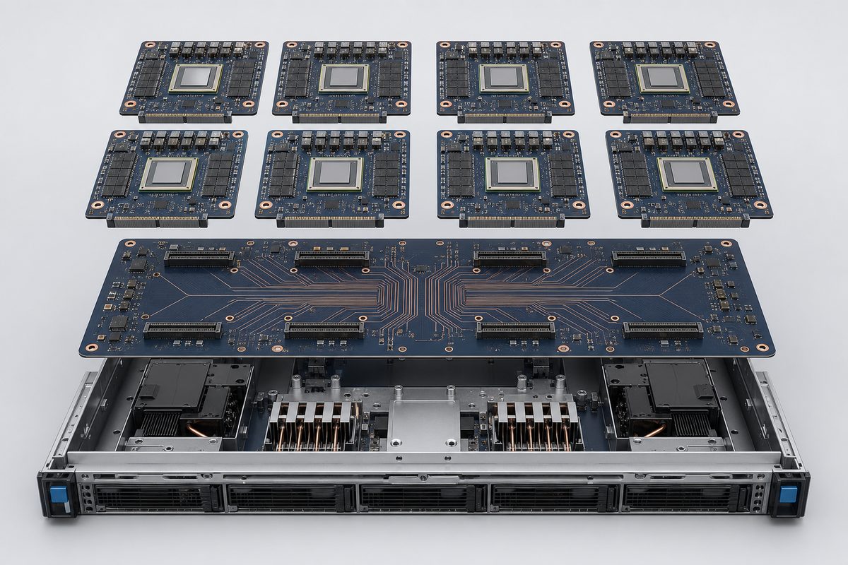
How Are Counterbores and Countersinks Drilled in PCBs?

PCB counterbores and countersinks are normally produced as controlled secondary machining features around a defined mounting hole, although the exact sequence depends on the factory process, plating requirement, tool, and panel support. The finished geometry and board condition matter more than assuming one universal drilling sequence.

  1. Verify the released drill data, fabrication drawing, stack-up, finished thickness, and machining side.
  2. Create or reference the finished mounting hole according to its plated or non-plated requirement.
  3. Machine the cylindrical pocket or conical seat with a qualified tool and controlled setup.
  4. Remove burrs or loose laminate without changing the specified diameter, depth, or angle.
  5. Inspect geometry, copper and mask condition, and the fit of the specified production fastener.

Counterhole data may be supported in NC Drill, ODB++, or IPC-2581 outputs, but a human-readable fabrication drawing should still confirm the side, diameter, depth or angle, tolerance, and plating intent. For projects continuing through PCB assembly, include the enclosure stack-up and any installation constraint that affects screw fit or torque.

How to Dimension a Hole With a Counterbore or Countersink?

Dimension the mounting hole and recess as one controlled mechanical feature, with every value needed for machining and inspection. Do not make the fabricator reverse-engineer the screw head or choose between conflicting drill notes, drawings, and 3D models.

  1. Identify hole quantity and XY location from controlled datums.
  2. State whether each recess is on the top, bottom, or both sides.
  3. Specify the finished through-hole diameter and plated or non-plated condition.
  4. Specify the recess diameter.
  5. For a counterbore, specify depth from the machined surface.
  6. For a countersink, specify included angle and either maximum diameter or depth.
  7. Add tolerances based on functional fit and a practical inspection method.
  8. Define the required screw position: flush, below flush, or controlled protrusion.
  9. Show copper, solder-mask, component, and board-edge keep-outs around the complete recess.

Release one controlled value for each dimension. Include Gerber or another accepted PCB image format, drill data, fabrication drawing, stack-up and finished thickness, and a current STEP or mechanical model when enclosure fit is critical. If these sources disagree, production should stop for clarification.

What Are Common Counterboring and Countersinking Mistakes?

Common counterboring and countersinking mistakes begin with the wrong fastener, incomplete callouts, or clearances based only on the small mounting hole. Most can be found during DFM review before material is removed.

  • The drawing does not state the machined side.
  • The countersink angle does not match the purchased flat-head screw.
  • Counterbore depth is measured from the wrong reference surface.
  • The copper keep-out is based on D1 instead of the larger D2 recess.
  • The feature removes too much laminate from the minimum finished board thickness.
  • The mounting hole’s plated or non-plated condition is missing.
  • The screw head fits, but the driver, washer, standoff, or nearby component does not.
  • An ordinary twist drill is assumed to produce a controlled flat-bottom counterbore.
  • Tolerances are copied from metal machining without considering PCB material or inspection.
  • The drill table, fabrication notes, and mechanical model contain different values.

A DFM review should return these discrepancies to the designer before drilling or routing. EBest Circuit lists countersunk and counterbore-hole work among its FR4 PCB manufacturing support areas, but every special recess still requires project-specific review rather than a generic capability assumption.

How Should the Finished PCB Feature Be Inspected?

Inspection should verify geometry, surface condition, remaining material, and functional fastener fit. A diameter check alone cannot confirm that the screw seats at the required height or that the recess was machined from the correct side.

  1. Confirm hole count, location, machining side, and visible surface condition.
  2. Measure the finished through-hole and recess diameters.
  3. Measure counterbore depth or countersink angle or depth with suitable equipment.
  4. Check for exposed or damaged copper, lifted mask, delamination, burrs, and laminate breakout.
  5. Install the specified production fastener and verify flushness or recessed height.
  6. Confirm driver access and component, standoff, or enclosure clearance.
  7. Where electrical isolation matters, verify separation from copper and chassis metal.
Quality inspection of countersink and counterbore PCB holes with optical measurement and depth checking

For first articles, retain the measurement record and approved fastener-fit sample. These references make later checks more repeatable than a drawing note that only says the screw must be flush.

FAQ About Counterbore vs Countersink

What is the difference between countersink and countersunk?

A countersink is the conical feature or the cutting operation. Countersunk describes a hole or fastener that has already been formed or seated in that feature. For example, a drawing may specify a countersink, while the completed assembly uses a countersunk screw.

Why is it called counter sunk?

The term describes a fastener head being sunk into a prepared conical recess so it can sit flush or below the original surface. In technical writing, “countersink” is the noun or verb for the feature and operation, while “countersunk” usually describes the finished condition.

Can a countersink or counterbore be made on both sides of a PCB?

Yes, if the finished thickness and layer clearances support it. The drawing must identify which features are on the top, bottom, or both sides. Opposing recesses can leave very little laminate, so worst-case depth and thickness need a DFM check.

Should a PCB mounting hole be plated or non-plated?

The choice depends on grounding and mechanical requirements. If the screw connects to chassis ground, define the copper land and plating intent. If isolation is required, define the non-plated hole and full copper keep-out explicitly.

How do I choose the countersink angle?

Use the included angle from the actual flat-head screw specification. Do not assume a regional or CAD default. Confirm the part number, head diameter, and underside angle, then make the PCB callout match that hardware.

What is the correct speed for counterboring?

There is no single correct speed for every PCB counterbore. Tool diameter and material, laminate structure, spindle condition, depth, support, and machine capability all affect the qualified parameters. The manufacturer should set and validate the cutting conditions for the specific job.

Can a counterbore use a washer?

Yes, but the recess diameter and depth must fit both the washer and screw head. Check driver access and confirm that the remaining PCB section can support the wider bearing area without cutting into copper or nearby components.

Does a countersink weaken a PCB?

It can. The conical cut removes laminate around the mounting hole, and a thin board may lose a large share of its local thickness. Risk increases with a large recess, deep seating, limited edge distance, insufficient support, or high installation load.

Can metal-core PCBs use countersunk or counterbored holes?

They may be possible, but the stack-up, dielectric isolation, metal base, plating condition, and machining route require review. Do not transfer an FR4 counterhole design directly to an aluminum- or copper-base board without checking the complete structure.

Are counterhole dimensions stored in drill files?

Supported CAD tools can include counterhole data in NC Drill, ODB++, or IPC-2581 outputs. Even so, include a readable fabrication drawing that confirms the side, recess diameter, depth or angle, tolerance, and plating intent.

What tolerance should I use for a PCB counterhole?

Set tolerance from the functional fit and inspection method, then confirm it with the fabricator. Avoid copying an unnecessarily tight metal-machining tolerance into PCB laminate. The required screw seating position may be more useful than an isolated diameter tolerance.

What should I send for a counterhole DFM review?

Send the PCB image data, drill files, fabrication drawing, stack-up, finished thickness, screw drawing or part number, and STEP model. Include the required screw height, mounting side, enclosure interface, and electrical isolation or grounding requirement.

How Can EBest Circuit Review Your Mounting-Hole Design?

Send us the PCB fabrication package, stack-up, finished thickness, fastener specification, and mechanical model. Our engineering team can review the counterhole callout, machined side, remaining laminate, copper clearance, fastener fit, and assembly constraints before production. For PCB fabrication or full PCBA support, contact EBest Circuit at sales@bestpcbs.com with your Gerber files, quantity, and project requirements.

You may also like

PCB Interposer: Stackup, Routing, DFM, and Testing

August 13th, 2026

A PCB interposer is an intermediate printed circuit board that remaps pads, pins, power rails, or signals between two incompatible interfaces. Typical uses include adapting a new BGA to a legacy footprint, expanding a fine-pitch device into a testable array, and connecting boards or sockets with different pin assignments. Its design must control the complete transition from the first pad field through vias and routing to the second interface.

Organic PCB interposer with dense BGA pads and routed copper connections

Do You Need an Organic PCB Interposer or a Package-Level Interposer?

Choose the supplier from the interconnect level, not from the word interposer. An organic PCB interposer is fabricated with laminate, copper circuitry, plated holes or microvias, solder mask, and a board-level surface finish. A silicon interposer uses semiconductor processes and may contain through-silicon vias. Glass and advanced package substrates also require different fabrication equipment and qualification methods.

Structure Connection Level Typical Fabrication Route Primary Design Constraint
Organic PCB interposer Package-to-board, board-to-board, socket, or test interface Multilayer PCB or HDI processes BGA escape, via geometry, planarity, impedance, and assembly
IC package substrate Die or package to system board Fine-line organic substrate processes Package warpage, fine pitch, and substrate reliability
Silicon interposer Die-to-die or die-to-package in 2.5D integration Semiconductor lithography, often with TSVs Microbump density, TSV design, and thermal stress
Glass interposer Advanced package redistribution Specialized glass-via and metallization processes Via formation, metallization adhesion, and handling

If the input data contains bare-die bumps, microbumps, TSVs, redistribution layers, or package-level warpage requirements, route the project to an advanced-packaging supplier. If both sides are conventional pads, BGA lands, connectors, sockets, or test contacts that can be built with PCB processes, continue with an organic PCB feasibility review.

Which Inputs Must Be Fixed Before Stackup Design?

Freeze both mating interfaces and their electrical mapping before selecting layer count or via type. The design team needs controlled coordinates, orientation, pin names, mechanical datums, installed height, attachment method, and service conditions for both sides. A mirrored footprint or outdated pin map can produce a board that passes fabrication inspection but connects the wrong nets.

  • Interface geometry: provide pad coordinates, package drawings, body outline, keepouts, datum locations, connector or socket drawings, and allowable positional error.
  • Pin mapping: identify every signal, ground, power, no-connect, reserved pin, polarity mark, and remapped connection in a controlled table.
  • Electrical limits: state impedance, current, voltage spacing, differential-pair skew, insertion-loss budget, and any sensitive analog or clock nets.
  • Assembly route: define soldered, socketed, compression-contact, or test-only use; also state which side is assembled first and the number of thermal cycles.
  • Mechanical limits: specify total thickness, flatness or coplanarity, component clearance, support points, contact force, and allowable board deflection.
  • Service profile: include operating and storage temperature, vibration, expected mating cycles, moisture exposure, cleanliness, and target life.

How Should the BGA Escape and Stackup Be Built?

Derive the stackup from routing channels, reference-plane continuity, and manufacturable via transitions. Start by grouping pins into ground, power, high-speed, low-speed, analog, clock, and unused classes. Then estimate how many traces must leave each BGA ring and which layer changes are unavoidable.

Engineer reviewing PCB interposer stackup and dense BGA escape routing
  1. Route the outer rows: use surface escape where trace width, clearance, and solder-mask geometry provide adequate manufacturing margin.
  2. Assign via structures: use through holes when pitch permits; introduce blind microvias or via-in-pad only where inner rows cannot escape otherwise.
  3. Reserve reference planes: keep controlled-impedance signals adjacent to continuous ground and provide nearby ground transitions at every signal-layer change.
  4. Distribute power: size copper and via arrays from current and transient requirements, then place decoupling where the connection inductance remains useful.
  5. Check lamination sequence: map each blind and buried via to a real build stage; stacked microvias and multiple sequential laminations require an explicit reliability review.

  6. Balance copper: correct large density differences between the central pad field and the perimeter to reduce bow, twist, and registration variation.

Via-in-pad must be called out as filled, capped, and planarized when the pad will be soldered. Leaving the construction undefined can cause solder loss into the via, insufficient joint volume, and uneven pad surfaces. Backdrilling may reduce through-via stubs, but it requires adequate stub access, drill tolerance, and clearance from adjacent structures.

Which Parameters Control Signal and Power Integrity?

Analyze the pad, via, trace, plane reference, and mating joint as one electrical discontinuity. Short interposers can still degrade fast interfaces because their transitions may contain large pads, long via stubs, anti-pad changes, or interrupted return paths.

  • Impedance: calculate from the proposed production stackup, including finished copper, dielectric thickness, resin content, trace geometry, and fabrication tolerance.
  • Return path: prevent plane splits and voids below fast routes; place ground vias close to signal vias when the route changes layers.
  • Via discontinuity: evaluate barrel length, unused stub, pad diameter, anti-pad diameter, and nearby ground-via placement.
  • Differential symmetry: match the two paths through pads and vias, not only along straight traces; control intra-pair skew at the transition.
  • Crosstalk: evaluate spacing together with parallel length, edge rate, reference distance, and allowable coupled noise; a fixed spacing ratio is not a universal acceptance rule.
  • Power impedance: minimize loop inductance through paired power-ground vias, suitable plane spacing, and decoupling connected with short, wide paths.

Use impedance coupons for fabrication control, TDR for time-domain discontinuity location, and S-parameters or an end-to-end link test when insertion loss, return loss, or crosstalk is part of the interface budget. Match the test method and frequency range to the actual signal instead of using a generic high-speed label.

What Manufacturing Limits Require an Early DFM Review?

No single minimum-feature value proves that a dense interposer is manufacturable. Pad pitch must accommodate trace escape, capture pads, anti-pads, solder-mask openings, registration allowance, copper thickness, via fill, and the selected lamination sequence at the same time.

Capability Item General Capability Special Process or Review
FR-4 layer count 1-10 layers; high-Tg material noted for 8 layers and above 10-32 layers
Laser blind or buried via diameter 0.10 mm Project-specific stackup review
Minimum finished mechanical hole 0.20 mm 0.15 mm
Through-hole aspect ratio 8:1 10:1
Inner-layer line/space at 0.5 or 1 oz 4/4 mil 3/3 mil
Outer-layer line/space at 1 oz 4/4 mil 3/3 mil
Solder-mask opening, single side 2 mil 1 mil
ENIG thickness Gold 0.025-0.125 micrometers; nickel 3-8 micrometers Confirm against pad function and assembly criteria

These values come from the current general PCB capability workbook and are feasibility boundaries, not automatic design rules. EBest Circuit must review the actual BGA map, copper weight, material, panel construction, via sequence, solder-mask strategy, and acceptance criteria before confirming a special-process design.

How Is an Organic PCB Interposer Manufactured?

Organic PCB production is the base process. Dense pad fields add tighter controls for registration, via filling, planarity, and copper balance.

  1. Verify data: compare the netlist, layer stack, drill pairs, pin map, dimensions, impedance notes, and finish requirements before tooling.
  2. Form inner layers: image and etch copper, then inspect line width, spacing, annular rings, and defects before lamination.
  3. Laminate the structure: control resin flow, dielectric thickness, copper distribution, and layer registration across each build cycle.
  4. Create interconnects: drill mechanical holes or laser microvias, desmear, metallize, and plate to the specified layer pairs.
  5. Fill via-in-pad: fill, cure, planarize, and cap solderable pads so that the assembly surface remains flat and sealed.
  6. Form outer layers: image and etch the final circuitry, then inspect critical pads, traces, and clearances.
  7. Apply mask and finish: control solder-mask registration and apply the approved surface finish for soldering or contact use.
  8. Profile and test: route the outline, inspect dimensions, perform electrical test, and complete the defined coupon or microsection checks.

Which Failure Modes Should the Design and Test Plan Control?

Each critical failure needs a defined prevention method and a measurable detection method. Continuity testing alone cannot detect planarity, joint fatigue, impedance discontinuities, or weak microvias.

Failure Mode Primary Cause Design Control Verification
Wrong net connection Mirrored footprint, orientation error, or uncontrolled pin-map revision Independent coordinate and netlist comparison Electrical test against the approved netlist
Solder wicking Open or incompletely filled via-in-pad Filled, capped, and planarized construction Cross-section and assembly inspection
Open or intermittent joint Warpage, contamination, inadequate solder volume, or unstable contact force Flatness, finish, stencil or socket, and support controls X-ray, coplanarity measurement, and continuity under load
Signal reflection Via stub, pad/anti-pad discontinuity, or reference-plane interruption Transition modeling and controlled return path TDR, S-parameters, or link test
Microvia fatigue Stacked geometry, high thermal stress, or unsuitable lamination sequence Via-structure and stackup reliability review Thermal cycling with resistance monitoring and cross-section
Pad or laminate damage Board bending, socket force, shock, or poor support Mechanical load-path and thickness review Strain measurement, mechanical test, or destructive analysis

How Should the Finished PCB Interposer Be Validated?

Validate in four stages: data correctness, bare-board quality, assembled-interface quality, and application performance.

Technician inspecting and probing a finished PCB interposer
  • Data comparison: verify fabrication data, drill pairs, stackup, netlist, and pin-map revision before production release.
  • Dimensional inspection: measure thickness, outline, datum locations, hole and pad positions, and bow or twist where mating alignment depends on them.
  • Electrical test: check opens and shorts; add four-wire resistance limits for low-resistance power or measurement paths when required.
  • Microsection: inspect plating, via fill, registration, dielectric condition, and interconnect structure on representative coupons or boards.
  • Assembly inspection: evaluate hidden solder joints by X-ray and inspect bridging, voiding, solder volume, wetting, and alignment against defined limits.
  • Signal verification: use impedance coupons, TDR, S-parameters, or a functional link test according to the electrical risk.
  • Reliability verification: select thermal cycling, vibration, mechanical loading, or mating-cycle testing from the actual service profile.

The purchase specification must name the test, sampling level, equipment or method, numerical acceptance limit, and disposition for failure. “100% electrical test” is meaningful only when the controlled netlist and tested characteristics are identified.

What Determines PCB Interposer Cost and Supplier Suitability?

PCB interposer cost is driven by the number of special operations and the manufacturing margin left around critical features. A small board can still be expensive when it requires sequential lamination, stacked or filled microvias, fine line/space, tight registration, controlled flatness, impedance coupons, or extensive inspection. Quantity and panel utilization matter, but they do not remove the cost of a complex build sequence.

Cost Driver Why It Changes the Quote RFQ Action
Layer and lamination structure Additional build cycles increase processing, registration control, inspection, and failure exposure. Request the proposed stackup and a layer-pair diagram for every blind or buried via.
Microvia and via-in-pad construction Laser drilling, filling, planarization, copper capping, and stacked structures add controlled operations. Identify which pads require filled and capped vias; do not apply the requirement to every via by default.
Fine features and tolerances Line/space, annular ring, solder-mask registration, positional accuracy, thickness, and flatness interact and can reduce yield margin. Mark each tolerance as functional, preferred, or open to supplier proposal.
Material and surface finish Material availability, stackup thickness, copper weight, finish type, and finish thickness affect sourcing and process compatibility. State the required electrical, thermal, soldering, or contact function instead of naming an unsupported substitute.
Electrical control Controlled impedance, low-resistance paths, and high-frequency limits require stackup calculations, coupons, or additional measurements. List the controlled nets, target values, tolerances, test method, and required report.
Inspection and reliability evidence Dimensional reports, microsections, X-ray, TDR, S-parameters, thermal cycling, and traceability add work only when specified as deliverables. Separate mandatory production acceptance from qualification or optional engineering tests.
Assembly responsibility Bare-board supply, solder-ball attachment, component assembly, socket integration, and functional testing have different tooling and quality ownership. Define the delivery state and assign responsibility for each mating interface.

Compare quotations only after normalizing their scope. One supplier may include via filling, impedance coupons, electrical test, dimensional reporting, and assembly inspection, while another may quote only the bare board. Ask each supplier to identify exclusions, special-process charges, tooling, test coverage, supplied reports, and the design changes assumed in the price.

A technically suitable supplier should return a manufacturable stackup, a complete via sequence, the features that consume the smallest process margin, and any proposed changes to pads, anti-pads, mask openings, copper balance, or tolerances. The response should also identify which operations are performed and controlled within its qualified supply chain. Silicon, glass, and bare-die package structures require an advanced-packaging route and should not be evaluated as conventional PCB work.

What Should Be Included in the Engineering Review Package?

The review package must reproduce both interfaces without assumptions. It must also control their mapping, board construction, and acceptance criteria.

  • Fabrication package: Gerber X2 or ODB++, NC drill files with layer pairs, IPC-356 or equivalent netlist, fabrication drawing, outline, and stackup.
  • Interface package: land-pattern coordinates, package and connector drawings, pin maps, orientation, datums, keepouts, and height limits.
  • Electrical package: net classes, impedance and skew limits, current by rail, voltage spacing, loss budget, and required measurements.
  • Material package: laminate performance requirements, copper weight, solder mask, surface finish, and restricted-substance requirements.
  • Assembly package: BOM where applicable, centroid data, paste intent, reflow limits, inspection criteria, and handling controls.
  • Quality package: acceptance class or customer specification, sampling, coupon plan, dimensional report, microsection criteria, traceability, and reliability tests.

Mark every requirement as mandatory, preferred, or open to supplier proposal. This prevents inherited layout habits from being treated as fixed system requirements and makes DFM changes auditable.

FAQs About PCB Interposer

Q1: Can one PCB interposer support several package variants?

A1: Only when the pad geometry and pin mapping remain unambiguous. Shared pads, jumpers, or option components must not create unterminated stubs, accidental shorts, or an assembly configuration that cannot be inspected.

Q2: When is a socketed interposer preferable to a soldered one?

A2: Use a socket when replacement, repeated testing, or device preservation is more important than minimum height and transition loss. Confirm contact resistance, force, wear, alignment, and bandwidth.

Q3: Does a thicker interposer improve reliability?

A3: Not automatically. Greater thickness can increase stiffness but also lengthen vias and change solder-joint or socket loading; evaluate electrical and mechanical effects together.

Q4: Can ENIG be used for every interposer contact?

A4: ENIG is common for solderable pads, but the contact function determines the finish. Repeated mechanical contacts, wire bonding, fine-pitch assembly, or special storage requirements may require another finish and separate confirmation.

Q5: When is backdrilling worth adding?

A5: Add backdrilling when the unused through-via stub consumes a meaningful part of the channel budget. Confirm remaining stub, drill tolerance, accessible side, and nearby-clearance limits before release.

Q6: Should unused BGA pads be removed?

A6: Remove or retain them only after checking routing space, assembly balance, inspection needs, and future variants. Unused pads must not be mistaken for connected or testable nodes.

Q7: How should orientation be controlled?

A7: Use at least two independent controls. Combine pin-one marking with asymmetric datums, keyed mechanical features, coordinate tables, or an assembly drawing that cannot be mirrored.

Q8: Is a functional test enough for production acceptance?

A8: Functional testing does not replace bare-board netlist testing or structural inspection. It may miss latent microvia, plating, dimensional, and process defects that have not yet caused system failure.

Q9: When should a test coupon be added?

A9: Add a coupon when production verification requires a representative structure that cannot be measured reliably on the finished board. Examples include impedance, plating, microvia, and lamination checks.

Q10: What must be controlled when the interposer is reworked?

A10: Limit cumulative heat, pad damage, laminate moisture, and mechanical bending. Define the permitted rework cycle, thermal profile, cleaning method, inspection, and acceptance test before reusing the assembly.

Conclusion

A reliable PCB interposer begins with controlled interface data and ends with measurable acceptance evidence. Freeze both pad fields and the pin map, derive the stackup from escape and reference requirements, review every via against the real build sequence, and connect each failure risk to a defined inspection or test.

For an organic PCB interposer review, send the fabrication data, pin maps, stackup, impedance targets, assembly method, service profile, and acceptance criteria to sales@bestpcbs.com. EBest Circuit will review the printed-board construction and identify features that require special-process confirmation.

You may also like

K Factor for Copper: Bending, Busbars and Voltage Drop

August 13th, 2026

The k factor for copper can mean two different engineering constants. In sheet-metal work, it is a dimensionless value that locates the neutral axis during bending. In wire calculations, K is a resistivity constant used to estimate voltage drop. Mixing these definitions can produce a wrong flat pattern or a wrong conductor size.

For copper sheet, formed terminals, and rigid busbars, practical bend calculations often start around 0.35 for soft copper, 0.407 for half-hard copper, and 0.452 for hard copper. These are starting values, not universal settings. Copper temper, thickness, inside radius, grain direction, and tooling must be confirmed before production.

K Factor for Copper shown on a 90-degree copper busbar bend

What Does K Factor for Copper Mean?

For bending, copper K-factor is the neutral-axis distance from the inside bend surface divided by material thickness. If the neutral axis sits 0.4 mm from the inside surface of a 1.0 mm sheet, K equals 0.40.

The metal inside a bend compresses while the outside stretches. Between those zones is a layer that keeps nearly the same length: the neutral axis. Its position determines how much material the bend consumes in the flat pattern.

Neutral axis, inside radius, and thickness in a bent copper strip

A higher bending K places the neutral axis farther from the inside surface and increases bend allowance. A lower K moves it inward and shortens the allowance. This value is dimensionless; it is not copper resistivity and it is not thermal conductivity.

Meaning of K Typical unit Primary use
Bending K-factor None Flat patterns and bend allowance
Electrical K value ohm-cmil/ft Conductor voltage drop
Thermal conductivity, k W/m·K Heat-transfer analysis

What K Factor Should You Use for Copper Bending?

Use 0.35, 0.407, and 0.452 as practical starting values for soft, half-hard, and hard copper respectively, then validate the selected value with the actual material and forming setup. A generic CAD default such as 0.44 may be convenient, but it can shift holes, slots, and terminals when the bend is tight or the copper temper changes.

Copper condition Starting K-factor Use note
Soft or annealed copper 0.350 Confirm tight bends for thinning or surface cracking
Half-hard copper 0.407 Common initial value for formed copper parts
Hard copper 0.452 Use a suitable radius and verify springback

The table does not replace a bend database. The production value belongs to a defined combination of copper grade, temper, thickness, bend direction, inside radius, tool, and process. If any of those inputs changes, repeat the trial or use a proven setup record.

K Factor for Copper Sheet Metal

The k factor for copper sheet metal controls the developed blank dimensions before a copper cover, shield, contact, or formed terminal is cut. Start with a temper-based value, use the drawing’s actual inside radius, and keep the same dimensioning convention throughout the calculation.

Copper sheet is more sensitive than a generic CAD material label suggests. Annealed sheet can flow around a tighter radius, while harder sheet usually needs a larger radius and shows more springback. Rolled sheet is also directional. A bend across the rolling direction often behaves differently from a bend parallel to it.

Before releasing a flat pattern, define:

  • alloy or copper grade and temper;
  • finished thickness and applicable thickness tolerance;
  • inside bend radius and included angle;
  • bend direction relative to the grain;
  • tooling method, such as air bending, bottoming, or forming;
  • critical hole-to-bend and terminal dimensions.

Do not use K-factor to hide an unsafe radius. K adjusts developed length; it does not prevent cracking. If a radius is below the material and temper limit, revise the geometry or forming process.

K Factor for Copper Busbar

The k factor for copper busbar should be selected by temper, thickness, radius-to-thickness ratio, and bend orientation, then proven on the intended machine. Busbar errors are costly because a few millimeters of flat-length error can misalign terminals, preload a bolted joint, or reduce designed clearance.

Copper busbar being bent in a precision press brake

Flatwise bends use the busbar’s smaller dimension as the bending thickness. Edgewise bends deform the wide dimension and normally require different tooling, a much larger radius, and separate validation. The same equation may describe both, but the mechanical limits are not interchangeable.

Keep bend geometry separate from current capacity. The K-factor and bend allowance determine cut length. Cross-sectional area, temperature rise, enclosure conditions, joint design, and allowable loss determine ampacity. Our guides to copper busbar ampacity and copper busbar PCB construction address those electrical and structural decisions separately.

How Do You Calculate Bend Allowance for Copper?

Calculate copper bend allowance with BA = θ × (R + K × T), where θ is the bend angle in radians, R is the inside radius, K is the bending K-factor, and T is material thickness.

For a 90-degree bend, θ equals π/2, or about 1.5708. Consider a 2.0 mm half-hard copper sheet with a 2.0 mm inside radius and K = 0.407:

BA = 1.5708 × (2.0 + 0.407 × 2.0) = 4.42 mm

If the two straight legs are measured to the tangent points and are 30 mm and 45 mm, the developed length is:

30 + 4.42 + 45 = 79.42 mm

For several bends, calculate each allowance separately. Do not assume that every bend uses one K or radius. Add the straight tangent-to-tangent segments and all allowances, then round once at the final drawing precision.

Bend deduction is an alternative when the drawing uses outside dimensions. Either method can work, but mixing outside dimensions, tangent dimensions, and centerline dimensions in one calculation will not.

How Can You Find the Actual K Factor From a Test Bend?

Find the production K-factor by bending a measured coupon, measuring the resulting geometry, calculating the bend allowance consumed, and solving the bend equation for K. This is more reliable than copying a general table when the finished dimensions are critical.

  1. Cut a coupon from the production material batch and record its flat length and thickness.
  2. Bend it with the planned punch, die, direction, angle, and forming method.
  3. Measure the inside radius, final angle, and straight tangent lengths after springback.
  4. Calculate bend allowance: flat length minus the two tangent-to-end straight lengths.
  5. Solve K = (BA/θ − R) / T.
  6. Repeat the bend to confirm that the result is stable, then store it with the complete setup record.

Use calibrated measurement methods. An assumed inside radius can corrupt the result even when the flat length is measured accurately. For recurring production, maintain a bend table by material, thickness, radius, and tool instead of relying on a single copper value.

Which Variables Change the Copper K Factor?

Copper K-factor changes when material behavior or the deformation path changes. The largest practical drivers are temper, radius-to-thickness ratio, bend direction, tool geometry, and forming method.

  • Temper: softer copper yields more readily; harder copper generally needs more radius and springback control.
  • R/T ratio: changing the inside radius relative to thickness changes strain distribution and the neutral-axis position.
  • Grain direction: rolling direction affects cracking risk and repeatability, especially on tight bends.
  • Tooling: punch nose, die opening, tool wear, and alignment affect the actual radius and angle.
  • Forming method: air bending, bottoming, wiping, and dedicated forming tools do not produce identical results.
  • Part geometry: nearby holes, slots, embosses, plated areas, or width transitions can redistribute strain.

Springback changes the final angle rather than the theoretical neutral-axis location alone, but it must be calibrated with K because both affect the finished coordinates. A correct blank with the wrong recovered angle still fails to fit.

What Is the K Factor for Copper Wire?

For voltage-drop calculations, the k factor for copper wire is commonly taken as 12.9 ohm-cmil/ft at 75°C in the referenced conductor-resistance convention. This K is not the dimensionless bending value.

Copper wire voltage-drop test with source, load, and multimeters

A common single-phase estimate is VD = 2 × K × I × L / CM. I is current in amperes, L is one-way length in feet, and CM is conductor area in circular mils. For a three-phase circuit, use 1.732 in place of 2.

For example, a 40 A single-phase load on 100 ft one-way copper conductors with 41,740 circular mils gives:

VD = 2 × 12.9 × 40 × 100 / 41,740 ≈ 2.47 V

This is an estimate. Conductor temperature, AC impedance, power factor, terminations, and installation conditions can change real voltage drop. Cable selection must also satisfy ampacity, protection, temperature rating, and applicable code requirements.

How Do Bending K Factor, Electrical K Value, and Thermal Conductivity Differ?

They differ in physical meaning, units, and formula. Use the equation’s units as a quick check before inserting a copper value.

Property Typical copper reference Used to calculate
Bending K-factor About 0.35–0.452 as temper-based starting values Bend allowance and flat length
Electrical K value 12.9 ohm-cmil/ft at 75°C Conductor voltage drop
Thermal conductivity, k Material- and temperature-dependent, in W/m·K Heat flow and thermal resistance

Do not paste 12.9 into a CAD bend table, and do not use 0.407 in a voltage-drop equation. Thermal conductivity is another separate material property; it belongs in a thermal model, not in either of these K-factor formulas.

What Errors Cause Wrong Copper Flat Patterns?

Wrong copper flat patterns usually come from an incorrect radius, the wrong dimensioning convention, or an unverified default K-factor rather than difficult arithmetic.

  • Using one generic K for every copper temper: the neutral-axis location and springback do not remain constant.
  • Using nominal instead of formed radius: the tool and process determine the actual inside radius.
  • Measuring legs to bend centers: bend allowance calculations normally need tangent-point lengths.
  • Combining allowance and deduction: choose the method that matches the drawing dimensions.
  • Ignoring grain and edge condition: a mathematically correct flat can still crack during forming.
  • Rounding each bend: small rounding errors accumulate across multi-bend copper parts.
  • Releasing holes too close to the bend: deformation can oval holes or move terminal features.

For production, connect the flat-pattern calculation to the actual copper busbar manufacturing process. A drawing should identify the datum, radius, angle, finished critical dimensions, material condition, and inspection method.

FAQ About K Factor for Copper

Is 0.44 always the correct K factor for copper bending?

No. A value near 0.44 may be a CAD default or a useful starting point for some setups, but copper temper, radius, thickness, tooling, and bend direction can require a different value.

What is the best starting K factor for soft copper?

Start around 0.35 for soft or annealed copper, then verify it on a coupon made with the intended radius and tooling.

Can one copper busbar use several K-factors?

Yes. If bends use different radii, orientations, or processes, calculate and validate them separately rather than assigning one K to the entire part.

Does copper thickness change K-factor?

Thickness affects the radius-to-thickness ratio and the strain path. A K value proven for one thickness should not be assumed valid for another without checking.

What is the difference between K-factor and bend deduction?

K-factor locates the neutral axis. Bend deduction is a dimensional amount subtracted from outside flange dimensions to obtain flat length. K is one input used to calculate bend allowance and deduction.

Is the K factor for copper and aluminum the same?

No. In both bending and voltage-drop work, copper and aluminum have different material properties. Use values and validation data for the specified material rather than substituting one for the other.

Is the K factor for copper cable different from copper wire?

In a voltage-drop equation, the same copper resistivity convention can apply, but cable construction and installation affect temperature, AC impedance, and allowable ampacity. Those conditions still need separate checks.

Does XLPE insulation change copper’s electrical K value?

XLPE does not change copper’s intrinsic resistivity, but its temperature rating and installation conditions influence conductor operating temperature, which changes resistance and voltage drop.

Can thermal conductivity be called the K value for copper?

It is often written as lowercase k, but it is measured in W/m·K and describes heat transfer. It is unrelated to the dimensionless sheet-metal bending K-factor.

When should a test bend be mandatory?

Use a test bend when terminal position is critical, material or tooling has changed, the bend is tight, the copper is hard, or a repeated part is moving from prototype to production.

How Can EBest Circuit Support Copper-Intensive PCB and Busbar Projects?

At EBest Circuit, we help engineering and procurement teams coordinate copper-intensive PCB and PCBA requirements with the mechanical and electrical interfaces around the board. That may include heavy copper PCB requirements, current paths, mounting features, busbar connection points, and assembly fit.

For a useful review, send us the Gerber files, stackup or copper-weight requirement, fabrication drawing, BOM, quantity, and any busbar or formed-copper drawing that controls the interface. If the design includes critical bends, include copper grade, temper, thickness, radius, angle, finished dimensions, and the proven bend table where available. You can also review our heavy copper PCB capabilities before submitting the package.

If you are unsure which k factor for copper belongs in the drawing, tell us whether the task is flat-pattern development, voltage-drop estimation, or thermal analysis. Email the project files and questions to sales@bestpcbs.com for review and quotation.

You may also like