PCB manufacturing PCB manufacturing
Home > Blog

epag surface finish

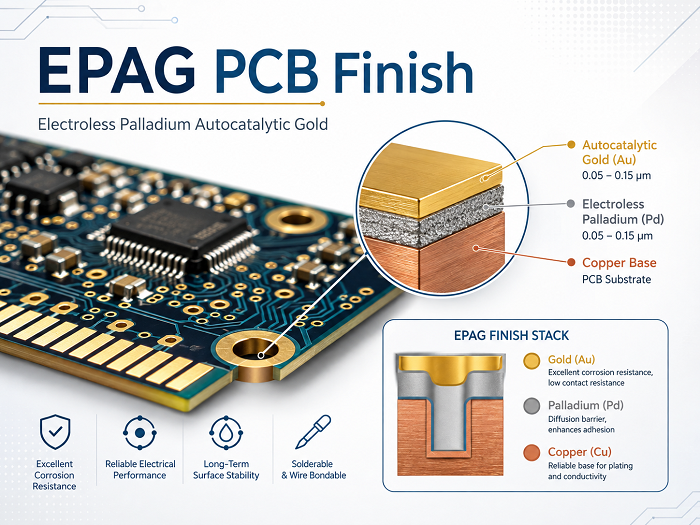
EPAG PCB Finish: Electroless Palladium Autocatalytic Gold Guide
Tuesday, August 18th, 2026

An EPAG PCB finish deposits electroless palladium directly over copper and adds an autocatalytic gold layer without nickel. It is a specialized option for qualified wire bonding, fine features, flex circuits, and exposed RF conductors where removing nickel provides a measurable benefit.

EPAG is not necessary for every PCB. It is mainly considered for wire-bonding applications, fine-feature designs, flex circuits, and high-frequency boards where removing nickel offers a practical benefit. This guide explains how EPAG works, how it compares with EPIG, ENIG, and ENEPIG, and what engineers and buyers should specify before requesting a quote.
EPAG PCB Finish: Electroless Palladium Autocatalytic Gold Guide

What Is EPAG (Electroless Palladium Autocatalytic Gold)?

EPAG stands for Electroless Palladium Autocatalytic Gold.

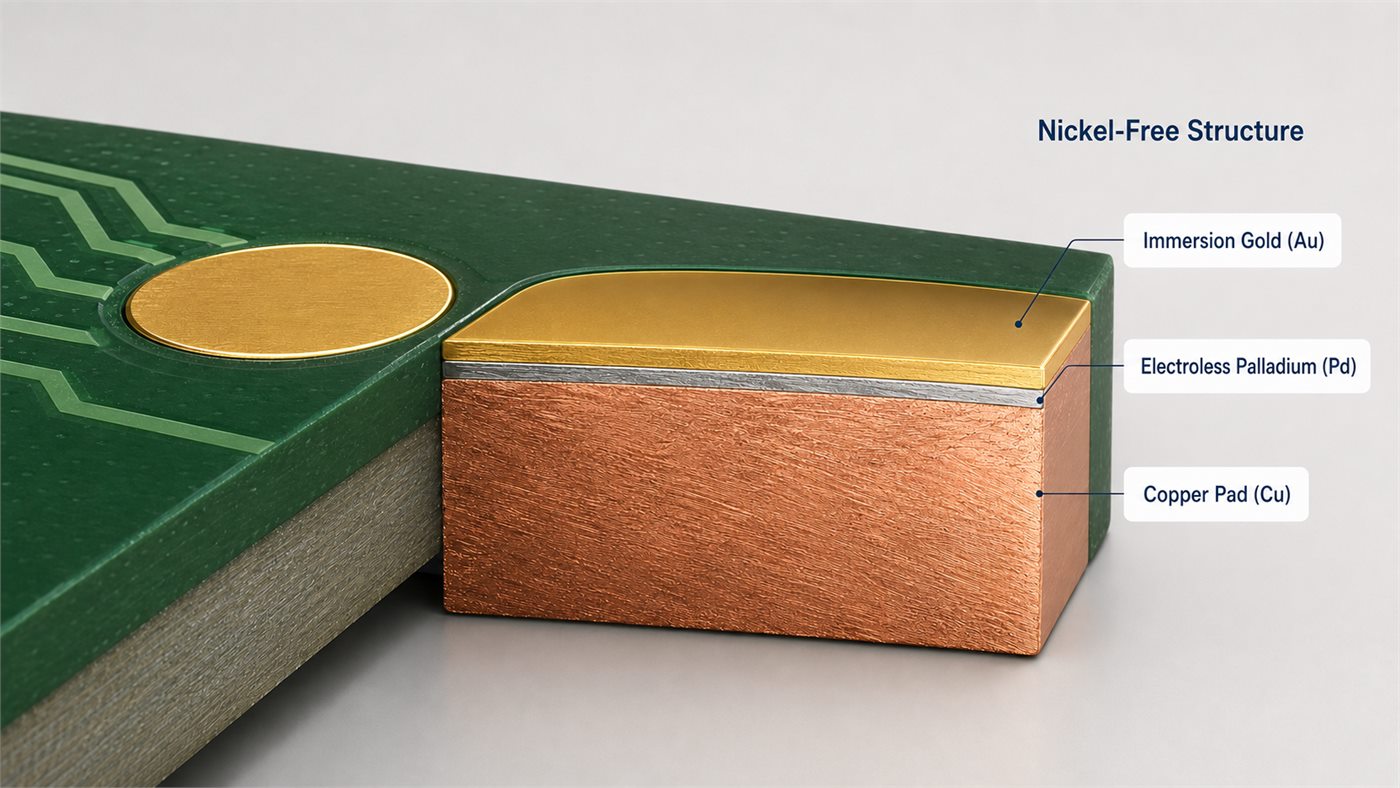
Copper → Electroless Palladium → Autocatalytic Gold

The key difference from ENIG is the absence of electroless nickel. Palladium is deposited over the exposed copper, followed by an autocatalytic gold layer.

This gives EPAG several useful characteristics:

  • nickel-free surface construction;
  • relatively low metallic buildup around fine features;
  • a solderable noble-metal surface;
  • compatibility with qualified wire-bonding processes;
  • potential advantages in RF and flex designs where nickel is undesirable.

The gold process is also important. Autocatalytic gold can continue depositing after the surface has been covered, which gives more control over functional gold thickness than a conventional immersion-gold process.

For this reason, EPAG should be specified as a complete surface-finish system rather than simply as “palladium gold.”
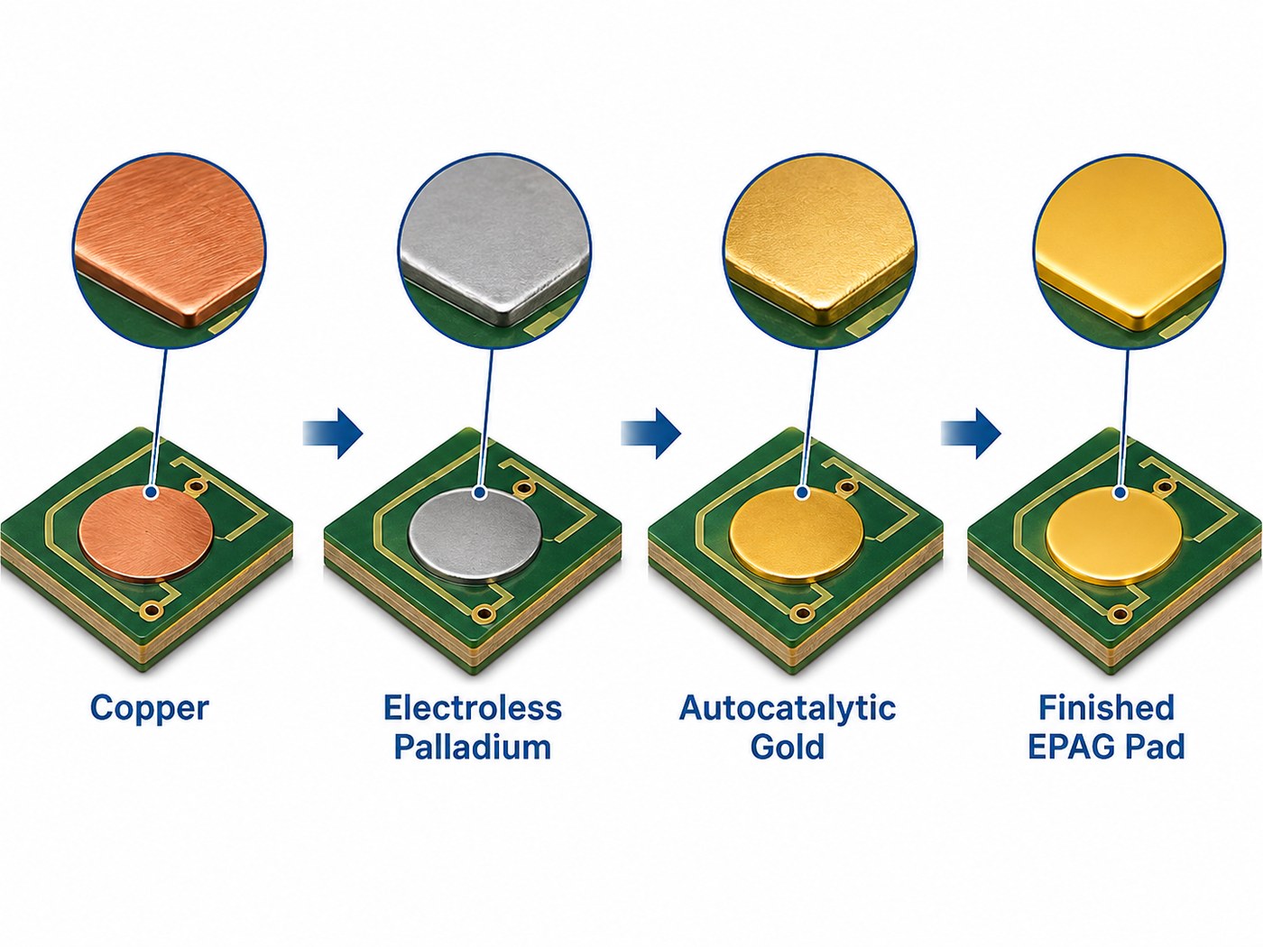
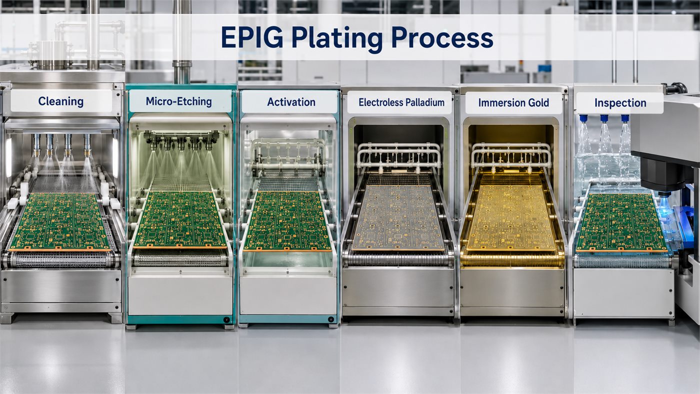
EPAG PCB plating process from copper to electroless palladium and autocatalytic gold

How Is EPAG Plated on a PCB?

The exact chemistry varies between plating systems, but a typical EPAG plating process follows four main stages.

  1. Copper preparation: Exposed copper is cleaned and conditioned. Oxides and contaminants must be removed before palladium deposition.
  2. Electroless palladium plating: Palladium is chemically deposited on the copper without using external electrical current.
  3. Autocatalytic gold deposition: Gold is chemically reduced onto the palladium surface. Unlike a self-limiting immersion reaction, the process can continue building the gold layer.
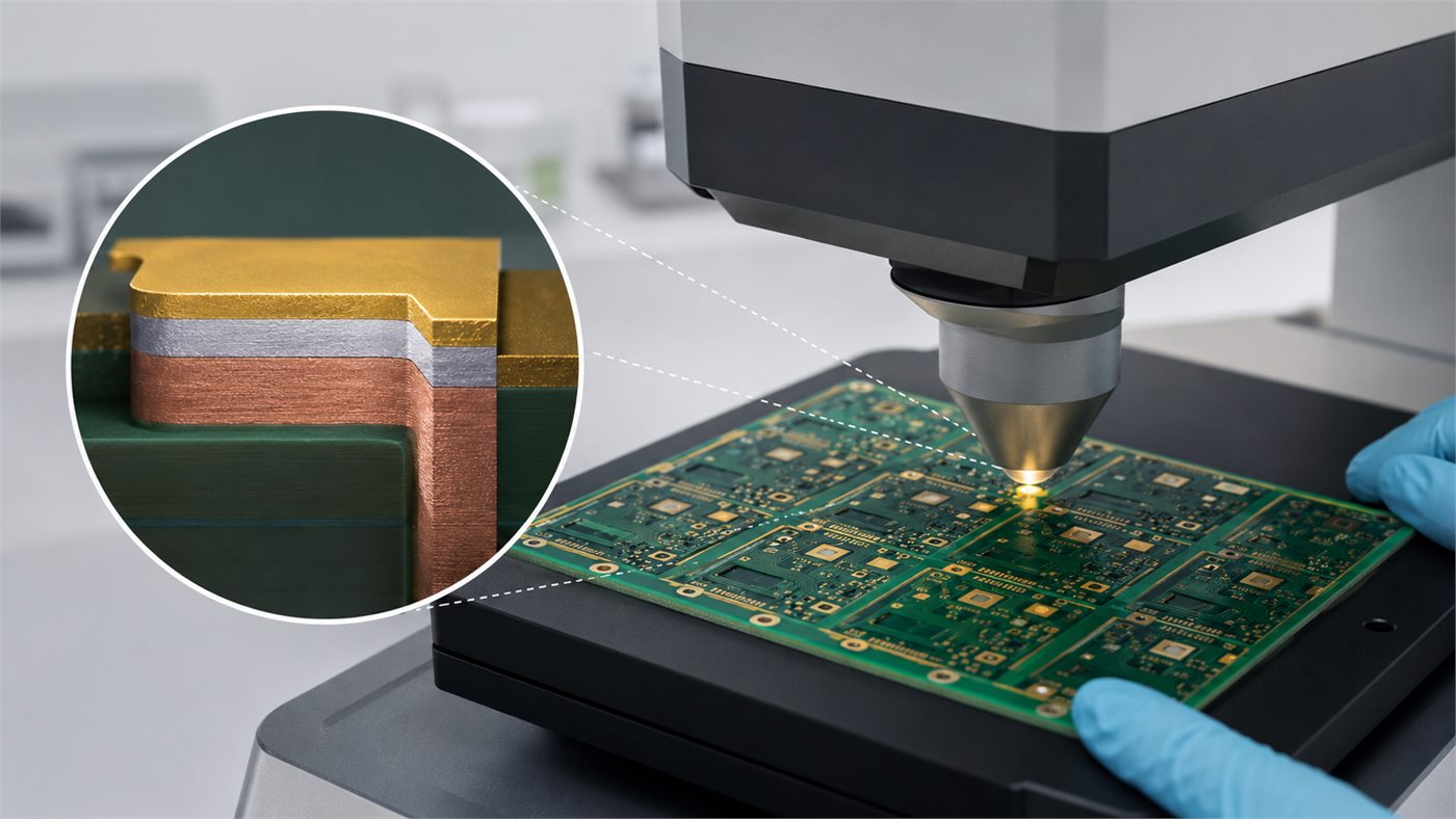
  4. Cleaning and inspection: The board is rinsed and checked for deposit consistency, thickness, solderability, and application-specific requirements.

The process is more specialized than standard ENIG. A PCB manufacturer needs suitable electroless palladium and autocatalytic-gold chemistry, stable bath control, and reliable thickness measurement.

If EPAG is essential to the design, confirm process availability before finalizing the fabrication drawing.

How Does Autocatalytic Gold Differ from Immersion Gold?

The main difference is how the gold layer grows.

Immersion gold relies on a displacement reaction. Gold deposits while a small amount of the underlying metal is displaced. As the surface becomes covered, deposition slows.

Autocatalytic gold uses a chemical reducing agent, so the gold surface can continue supporting further deposition. This makes it easier to build a thicker functional gold layer where required.

Feature Immersion Gold Autocatalytic Gold
Deposition method Displacement reaction Chemical reduction
Deposit growth Relatively self-limiting Can continue building
Typical role Protection and solderability Functional gold surface
Thickness flexibility More limited Greater
Wire-bond use Process-dependent More suitable when properly qualified

For ordinary solder pads, a thin protective gold layer may be sufficient. Wire-bond pads can require tighter control over gold thickness, purity, and surface condition. That is where autocatalytic gold becomes more valuable.

What Are the Advantages of EPAG PCB Finish?

EPAG is most useful when the design benefits from both a nickel-free stack and a controlled gold surface.

  • Nickel-free construction: useful when nickel is undesirable for electrical, magnetic, or mechanical reasons.
  • Fine-feature compatibility: removing the nickel layer reduces total metal buildup around small pads and tight clearances.
  • Wire-bond capability: properly qualified EPAG processes can support gold, silver, or copper wire bonding.
  • Solderability: palladium and gold provide a solderable, oxidation-resistant surface.
  • RF suitability: removing nickel can be useful on exposed high-frequency conductor areas.
  • Flex compatibility: eliminating the relatively hard nickel layer can help in flex designs where finished areas are close to bending zones.

These advantages matter only when they solve an actual design requirement. For a normal SMT control board, they may not justify a more specialized finish.

What Are the Limitations of EPAG Plating?

The first limitation is availability. EPAG is not offered by every PCB manufacturer that provides ENIG or ENEPIG.

Cost can also be higher because the process uses palladium and gold, and some applications require a more substantial gold deposit.

Specification quality is another concern. For critical applications, “EPAG finish” alone may not be enough. A complete requirement may need to define:

  • palladium thickness;
  • gold thickness;
  • solder-only or wire-bond surfaces;
  • bonding wire material;
  • selective plating areas;
  • storage requirements;
  • acceptance or qualification criteria.

For a standard SMT board with no RF, bonding, fine-feature, or nickel-related constraint, ENIG may remain the more practical choice.

EPAG vs EPIG: What Is the Difference?

EPAG and EPIG are both nickel-free palladium/gold finishes. The main difference is the gold deposition process.

For more detail on the alternative process, see our EPIG PCB surface finish guide.

Feature EPAG EPIG
Full name Electroless Palladium Autocatalytic Gold Electroless Palladium Immersion Gold
Layer concept Cu → Pd → autocatalytic Au Cu → Pd → immersion Au
Nickel layer No No
Gold process Autocatalytic Immersion
Gold build capability Greater More limited
Soldering Suitable Suitable
Wire bonding Strong option with qualified process Possible with suitable process
Fine-feature use Suitable Suitable
Main selection reason Functional gold layer Nickel-free finish with thinner gold

EPIG is often sufficient when the main goal is to remove nickel while maintaining a solderable palladium/gold surface. EPAG becomes more attractive when the gold layer itself needs to perform a more demanding function, especially in wire bonding.

EPAG vs ENIG: Which PCB Surface Finish Should You Choose?

For conventional SMT assembly, ENIG is usually the simpler starting point. EPAG becomes relevant when the nickel layer in ENIG creates a specific design concern.

Our ENIG PCB surface finish guide covers the nickel/gold process and its selection limits.

Selection Factor EPAG ENIG
Layer structure Cu/Pd/Au Cu/Ni/Au
Nickel-free Yes No
Standard SMT Suitable Very common
Wire bonding Suitable with qualified process Not usually the first choice
Fine features Lower metal buildup Nickel increases total deposit thickness
Flex applications Useful where nickel should be avoided Application-dependent
RF applications Attractive when nickel loss matters Common, but contains nickel
Availability Specialized Widely available
Sourcing simplicity Lower Higher

Choose ENIG when you mainly need a flat, solderable, widely supported finish.

Consider an EPAG PCB finish when the project involves:

  • exposed high-frequency conductors;
  • wire bonding;
  • very fine pad geometry;
  • repeated flexing near finished areas;
  • nickel-sensitive design conditions.

Changing from ENIG to EPAG without one of these reasons usually adds complexity without adding much value.
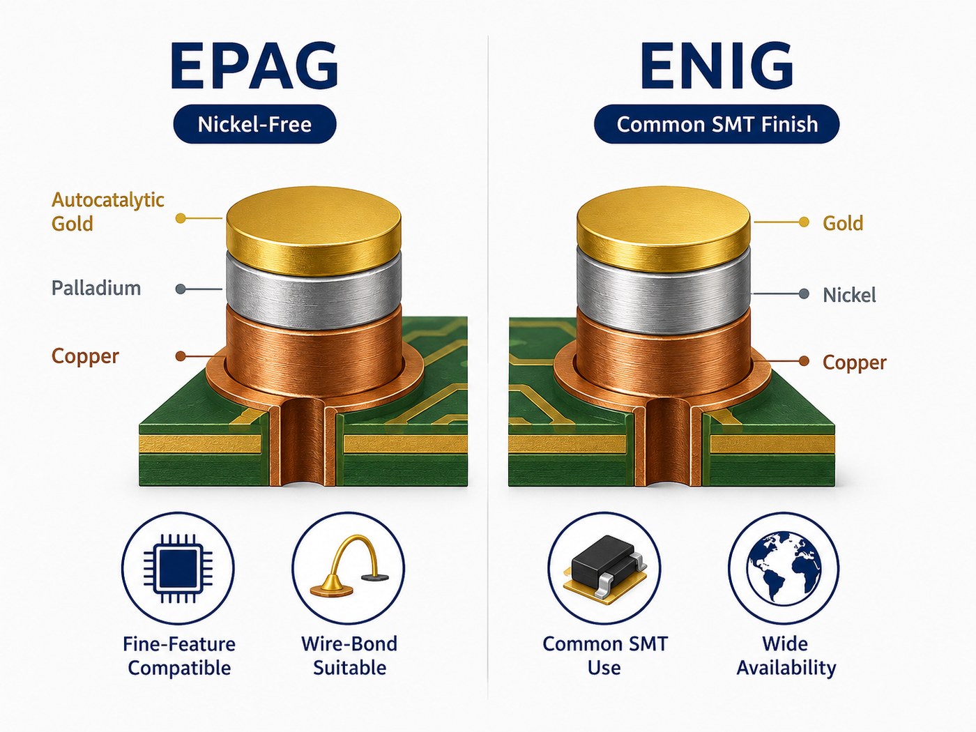
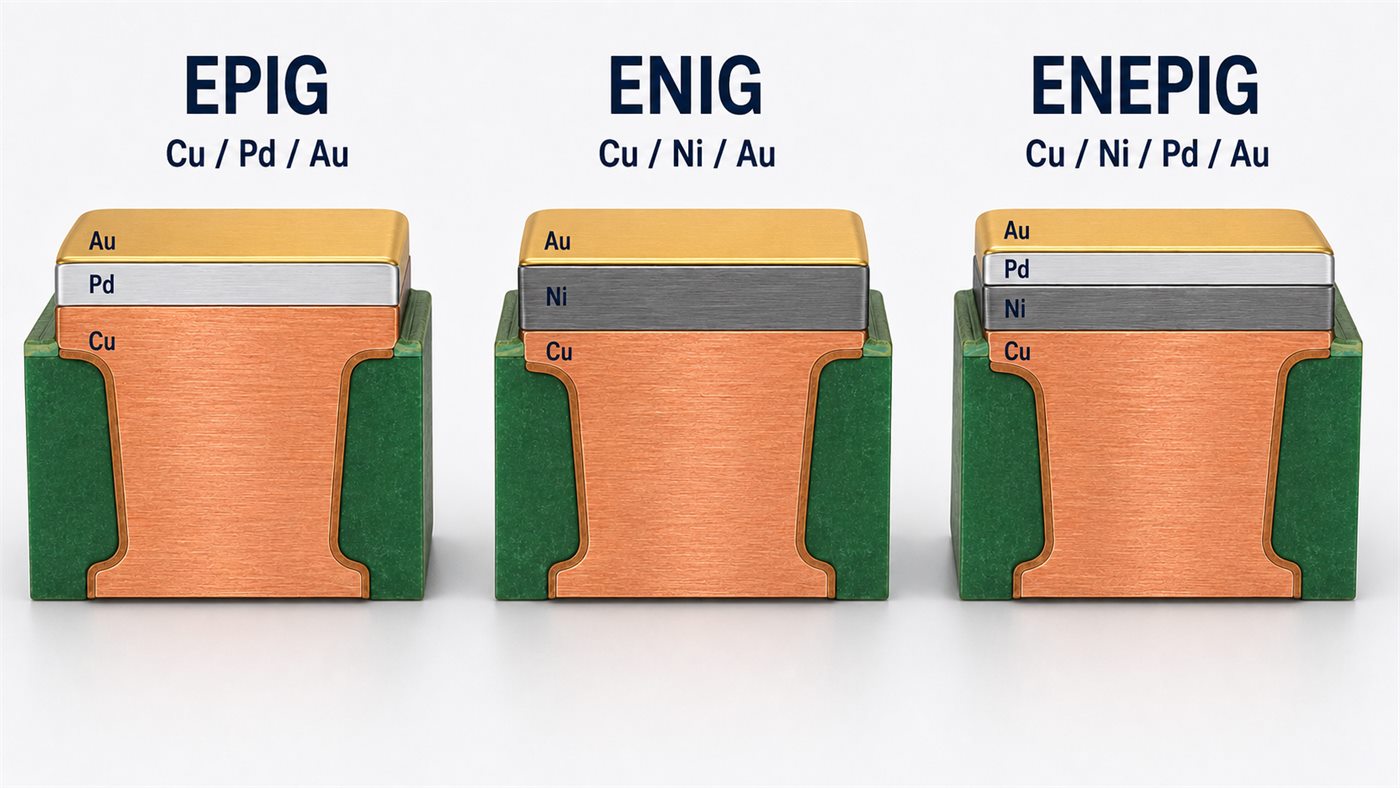
EPAG versus ENIG PCB surface finish comparison

EPAG vs ENEPIG: What Are the Key Differences?

ENEPIG and EPAG can both support soldering and wire bonding, but their metallic structures are different.

Feature EPAG ENEPIG
Layer structure Cu/Pd/autocatalytic Au Cu/Ni/Pd/immersion Au
Nickel No Yes
Palladium Yes Yes
Wire bonding Suitable Widely used
Soldering Suitable Suitable
RF consideration No nickel layer Nickel remains
Flex consideration Attractive where nickel should be avoided Nickel layer remains
Main selection reason Nickel-free functional gold Versatile soldering and bonding

ENEPIG is already a strong option when one PCB needs both soldering and wire bonding. EPAG should not replace it automatically. The case for EPAG becomes stronger when removing nickel provides a measurable electrical, dimensional, or mechanical benefit.

Is EPAG Suitable for Soldering and Wire Bonding?

Yes. EPAG can support both, provided the finish is specified and qualified for the intended assembly process.

For deposit-control context, compare the qualification points in our wire bonding EPIG thickness guide.

For soldering, the gold protects the palladium surface before assembly. The finished pad must still meet the solderability requirements of the selected assembly process.

Wire bonding needs tighter control. Important variables include:

  • gold thickness and purity;
  • surface cleanliness;
  • palladium condition;
  • bonding wire material;
  • wire diameter;
  • ball or wedge bonding method;
  • bonding force and temperature;
  • storage time before assembly.

A surface that looks visually acceptable is not automatically suitable for bonding. For a new production program, prototype bond testing is advisable when the plating chemistry, pad design, bonding wire, or bonding process has changed.
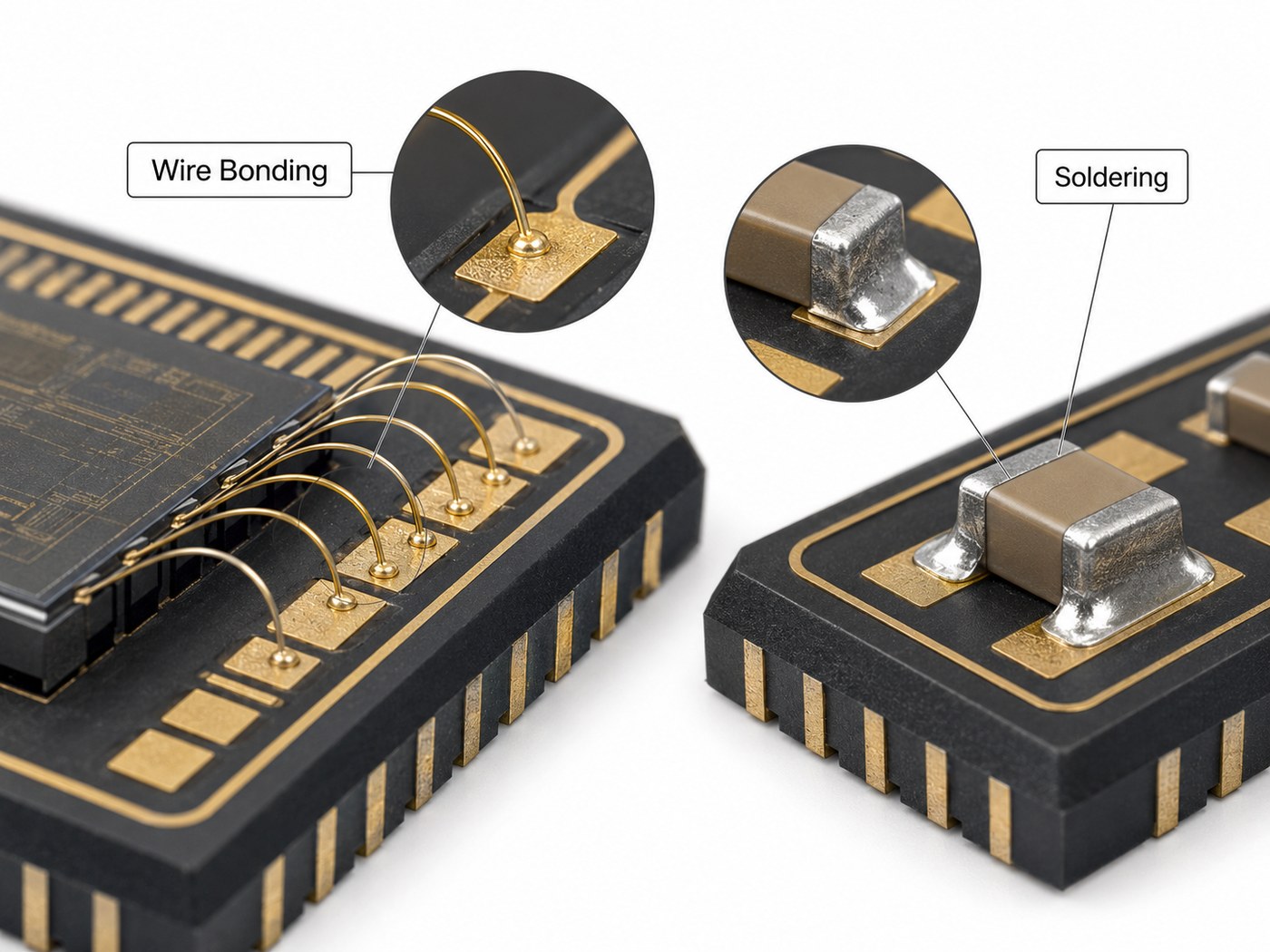
EPAG PCB finish for wire bonding and soldering

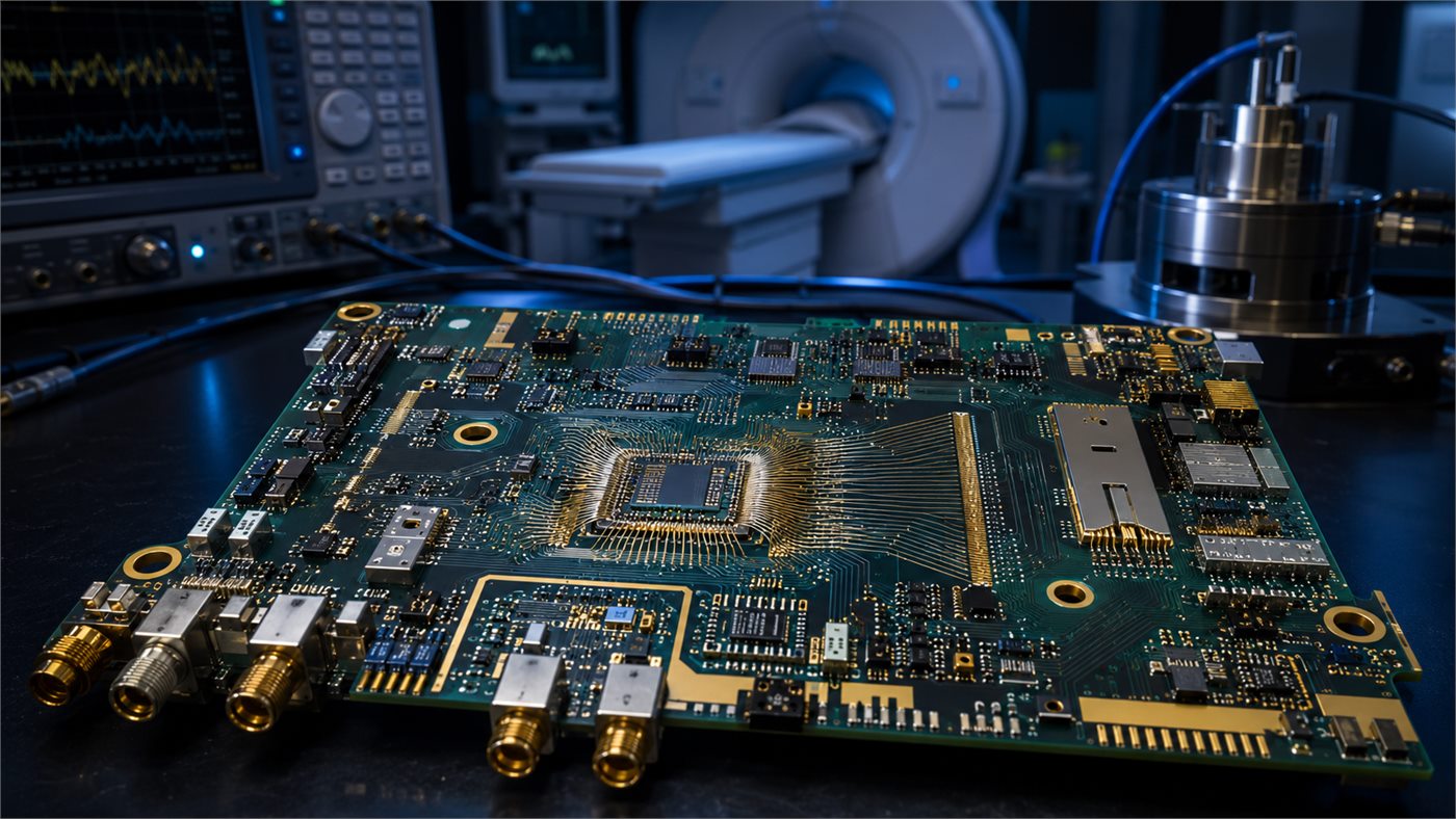
Why Is EPAG Used for High-Frequency and RF PCBs?

The main RF reason is simple: EPAG removes the nickel layer.

At high frequencies, current becomes concentrated near conductor surfaces because of skin effect. The metallic finish on those surfaces can therefore contribute to conductor loss.

Nickel has much lower conductivity than copper and also has magnetic properties. Removing it from exposed RF conductors can be useful when insertion-loss requirements are tight.

EPAG is worth considering when:

  • RF traces or launches contain exposed finished copper;
  • operating frequency is high;
  • insertion loss is tightly controlled;
  • fine RF features make plating buildup important;
  • nickel-containing surfaces are undesirable.

However, EPAG is not an automatic RF upgrade.

If most transmission lines remain under solder mask and only small component pads receive surface finish, other factors may have a much greater impact, including:

  • copper roughness;
  • dielectric loss;
  • impedance geometry;
  • stackup tolerance;
  • connector launches;
  • via transitions.

The finish should be selected according to where it actually appears in the RF signal path.
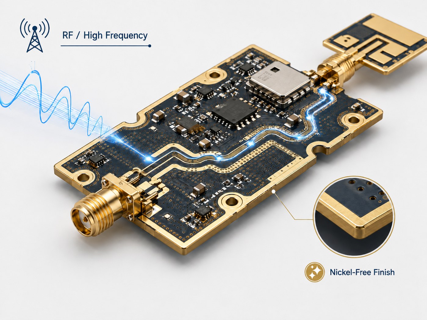
EPAG nickel-free finish for RF and high-frequency PCB applications

Can EPAG Be Used on Flex, HDI, and Ceramic PCBs?

Yes, but the reason for using EPAG changes with the PCB technology.

Flex PCB

A nickel-free finish can be useful near bending areas because nickel is relatively hard. EPAG may therefore be considered when finished conductors are exposed to repeated flexing.

HDI and fine-line PCB

Removing the nickel layer can reduce total plated buildup around small pads and closely spaced features. This can help preserve finished geometry in dense layouts.

Ceramic PCB

EPAG can also be considered for ceramic substrates, but compatibility depends on the conductor system rather than the ceramic material alone.

Examples include:

  • direct-bonded copper ceramic;
  • thick-film metallization;
  • thin-film metallization;
  • plated ceramic substrates.

These constructions may require different preparation and plating routes. Do not specify EPAG for a ceramic board based only on the substrate name. Confirm the exposed conductor metallurgy first.

What Should You Specify When Ordering an EPAG PCB?

An EPAG RFQ needs more information than a note saying “gold finish.”

Provide the PCB manufacturer with:

  • Surface finish: EPAG / Electroless Palladium Autocatalytic Gold
  • Board type: rigid, flex, rigid-flex, HDI, ceramic, etc.
  • Base material and stackup
  • Board thickness
  • Copper weight
  • Minimum trace and spacing
  • Minimum pad dimensions
  • Required palladium thickness, if controlled
  • Required gold thickness
  • Soldering requirements
  • Wire-bond requirements and wire material
  • Selective plating areas, if any
  • Controlled impedance or RF requirements
  • Inspection or qualification standard
  • Prototype and production quantities

Avoid copying a plating thickness from an older drawing unless you know why it was specified. Excessive gold can increase cost, while insufficient control can create problems in bonding applications.

At EBest Circuit, we can review the fabrication data, stackup, finish requirement, assembly method, and qualification needs during quotation. We confirm whether the proposed finish route fits the intended soldering, bonding, RF, or flex application before production.
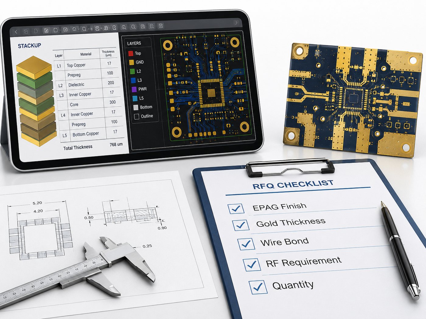
EPAG PCB RFQ checklist with stackup, gold thickness, wire bond, RF requirement and quantity

FAQs About EPAG PCB Finish

Is EPAG a nickel-free PCB surface finish?

Yes. EPAG uses electroless palladium over copper followed by autocatalytic gold, without an electroless nickel layer.

What is the difference between EPAG and EPIG?

Both are nickel-free palladium/gold finishes. EPIG uses immersion gold, while EPAG uses autocatalytic gold, which provides greater flexibility for building a functional gold layer.

Can EPAG be used for gold wire bonding?

Yes, provided the plating process, gold thickness, surface condition, and bonding parameters are qualified for the application.

Is EPAG better than ENIG for high-frequency PCBs?

Not always. EPAG can be useful when nickel on exposed RF conductors contributes to loss. If most RF traces are covered by solder mask, material loss, copper roughness, geometry, and connector transitions may matter more.

How should EPAG be specified on a PCB drawing?

Write Electroless Palladium Autocatalytic Gold (EPAG) and add controlled palladium or gold thickness where required. Wire-bond areas, bonding material, selective plating, and qualification requirements should also be identified.

How Can EBest Circuit Review Your EPAG PCB Requirements?

EPAG is valuable when its nickel-free structure and autocatalytic gold layer solve a real bonding, geometry, flex, or RF requirement. For routine SMT boards, a more widely available finish may remain the better purchasing choice.

Send us your Gerber or ODB++ files, stackup, quantity, finish specification, wire material, RF conditions, and deposit or qualification requirements. We will review manufacturability, confirm process availability, and prepare a quotation without assuming that one finish fits every design.
You may also like

EPIG PCB Surface Finish: Process, Thickness, Benefits, and EPIG vs ENIG
Monday, July 27th, 2026

An EPIG PCB surface finish uses electroless palladium directly over copper, followed by a thin immersion gold layer. This EPIG PCB finish is nickel-free and can support fine features, high-frequency circuits, soldering, and qualified wire bonding.

An EPIG PCB should be selected only when its layer structure solves a defined electrical, dimensional, magnetic, or bonding requirement. Comparisons with an EPAG surface finish must also account for the different gold-deposition process and achievable gold thickness.

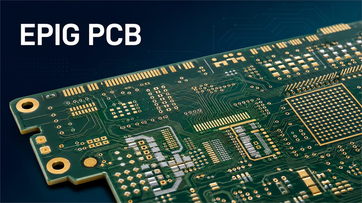
EPIG PCB with gold-finished pads and fine-pitch circuitry

EPIG, short for electroless palladium immersion gold, is a nickel-free PCB surface finish designed for fine features, high-frequency circuits, soldering, and wire bonding. Its copper-palladium-gold structure removes the relatively thick nickel layer found in ENIG and ENEPIG.

That difference matters when conductor spacing, magnetic behavior, or signal loss is sensitive to the surface-finish structure. However, EPIG is not automatically the best choice for every board. It has a less mature supply base than ENIG, requires tight process control, and may add cost without providing a meaningful benefit to an ordinary digital or industrial PCB.

This guide explains how EPIG is produced, how its thickness should be specified, where it performs well, and what buyers should confirm before requesting a quotation. The finish should be evaluated together with the underlying PCB material and the required PCB testing plan.

What Is EPIG PCB Surface Finish?

EPIG is a metallic PCB surface finish in which electroless palladium is deposited directly onto exposed copper, followed by a thin immersion gold layer. The palladium acts as a barrier and bonding surface, while the gold protects it from oxidation during storage and assembly.

Unlike ENIG, EPIG contains no electroless nickel layer. This makes it useful when nickel is undesirable because of high-frequency loss, magnetic sensitivity, biocompatibility requirements, or the dimensional effect of plating on very fine conductors.

EPIG should not be treated as another name for immersion gold. “Immersion gold” alone usually refers to ENIG in PCB purchasing documents. A fabrication note must explicitly state EPIG if the required structure is copper-palladium-gold.

It is also different from electrolytic hard gold. EPIG is intended mainly for solderable pads and wire-bonding surfaces. It is not the default choice for edge fingers or sliding contacts that require a wear-resistant hard-gold deposit.

What Is the Layer Structure of an EPIG Finish?

An EPIG finish uses fewer metallic layers than ENIG or ENEPIG. That simpler structure is the source of many of its electrical and dimensional advantages.

Labeled EPIG layer structure showing immersion gold, electroless palladium, and copper
Layer Main Function Manufacturing Concern
Immersion gold Protects palladium from oxidation and preserves the assembly surface Porosity, uniformity, storage condition, and thickness
Electroless palladium Provides a diffusion barrier and supports soldering or wire bonding Bath stability, adhesion, phosphorus content, and deposit thickness
Copper pad Provides the conductive base Cleanliness, micro-etch depth, surface activation, and roughness

Because palladium is deposited directly on copper, copper preparation is critical. Contamination, excessive micro-etching, or incomplete activation can reduce adhesion and create localized plating defects.

The structure also avoids several micrometers of nickel build-up. This can be valuable where pads and traces have very small clearances, although surface finish alone cannot compensate for an unsuitable PCB design rule.

How Does the EPIG Plating Process Work?

EPIG plating process from cleaning through inspection
  1. Copper cleaning: Oils, fingerprints, solder mask residues, and other contaminants are removed from exposed pads.
  2. Micro-etching: A controlled amount of copper is removed to eliminate oxides and create an active, uniform surface.
  3. Conditioning and activation: The copper is prepared so that palladium deposition starts evenly across the panel.
  4. Electroless palladium deposition: Palladium is chemically deposited without an external electrical current. Bath temperature, pH, metal concentration, reducing chemistry, and exposure time affect the deposit.
  5. Rinsing: Residual chemistry is removed without contaminating the next bath.
  6. Immersion gold deposition: Gold replaces a small amount of the palladium surface through a controlled chemical reaction.
  7. Final rinsing and drying: Water quality and drying conditions are controlled to prevent stains and ionic contamination.
  8. Inspection and testing: The fabricator may check coating thickness by X-ray fluorescence and perform solderability or bonding tests when specified.

EPIG quality depends more on bath control and copper preparation than on visual appearance alone. A bright, uniform surface does not prove that the palladium and gold thicknesses meet the drawing.

What Is the Typical EPIG Plating Thickness?

XRF inspection of palladium and gold coating thickness on an EPIG PCB

There is no single thickness range that should be copied into every EPIG drawing. Published process ranges vary with the chemical system, intended assembly method, and supplier capability.

Common industry references place electroless palladium at approximately 0.10-0.15 µm and immersion gold at approximately 0.10-0.20 µm. These values are useful as a starting point, not as an automatic purchasing specification.

  • Soldering may use a different process window from gold or aluminum wire bonding.
  • A gold layer that is too thin may provide inadequate protection during storage.
  • Excessive gold can alter solder-joint intermetallic formation and increase cost.
  • An insufficient palladium layer may provide an incomplete barrier between copper and gold.
  • A deposit optimized for wire bonding may require tighter surface and thickness controls.

Specify whether the values are nominal, minimum, or an acceptable range. Also state the measurement method and sampling plan if coating thickness is critical. For prototypes, confirm that the same chemistry and thickness window can be maintained in volume production.

What Are the Advantages of EPIG Surface Finish?

  • Nickel-free construction: Useful for non-magnetic products, nickel-sensitive medical applications, and circuits where nickel-related conductor loss is a concern.
  • Low metallic build-up: Supports fine lines, small pads, narrow gaps, and advanced HDI geometries.
  • Flat surface: Suitable for QFNs, BGAs, and other packages that need consistent pad planarity.
  • High-frequency potential: Removing nickel can reduce one source of conductor loss in RF and microwave designs.
  • Solderability: A controlled EPIG deposit provides a solderable surface for PCB assembly.
  • Wire-bonding capability: EPIG can support gold and aluminum wire bonding when its chemistry, thickness, and surface condition are qualified.
  • Corrosion protection: Palladium and gold protect exposed copper from oxidation before assembly.
  • Lead-free compatibility: EPIG can be used in RoHS-compliant PCB and PCBA production.

These advantages are application-specific. On a conventional four-layer controller operating at low frequency, ENIG may provide the required flatness and shelf life with broader availability and lower purchasing risk.

What Are the Limitations of EPIG?

EPIG remains less common than ENIG and ENEPIG. Fewer PCB factories maintain a qualified direct-palladium process, so buyers may face longer lead times, higher minimum charges, or limited options for urgent production.

  • Palladium and gold increase material and process costs.
  • The process requires stable bath chemistry and precise copper activation.
  • Thickness limits vary among suppliers.
  • Wire-bonding performance must be qualified against the actual wire, bonding parameters, and pad design.
  • Immersion gold is relatively thin and is not a substitute for wear-resistant hard gold.
  • Storage life depends on deposit quality, packaging, humidity, and handling.
  • Industry data and production history are less extensive than for ENIG.

EPIG is most economical when its nickel-free structure solves a defined problem. Selecting it only because it appears more advanced can increase sourcing complexity without improving product performance.

EPIG vs ENIG: What Is the Difference?

The choice is mainly determined by whether the design benefits from removing nickel. ENIG remains a practical default for many fine-pitch commercial boards, while EPIG serves more specialized electrical, dimensional, bonding, and non-magnetic requirements.

Labeled comparison of EPIG, ENIG, and ENEPIG PCB surface finish layers
Factor EPIG ENIG
Layer structure Copper/palladium/gold Copper/nickel/gold
Nickel present No Yes
Availability Limited Widely available
Fine-line build-up Lower Higher because of the nickel layer
High-frequency use Attractive when nickel-related loss matters Suitable for many designs, but losses should be evaluated
Wire bonding Possible with a qualified process Gold wire bonding is more restricted
Process maturity Emerging or specialized Mature and broadly used
Typical cost Often higher or less predictable Usually easier to source and price

For a standard SMT board, ENIG is usually easier to qualify and source. EPIG becomes more compelling when a simulation, spacing constraint, bonding process, or product requirement provides a clear reason to exclude nickel.

EPIG vs ENEPIG: Which One Should You Choose?

EPIG and ENEPIG both use palladium and gold, but ENEPIG retains an electroless nickel layer beneath the palladium.

Selection Factor EPIG ENEPIG
Structure Cu/Pd/Au Cu/Ni/Pd/Au
Nickel-free Yes No
Fine conductor spacing Lower deposit build-up Nickel adds thickness
High-frequency behavior Preferred where nickel loss must be minimized Requires evaluation of the nickel layer
Soldering Supported Well established
Gold and aluminum wire bonding Supported with process qualification Widely used for mixed assembly requirements
Supply availability More limited More widely available

Choose EPIG when the absence of nickel is a design requirement. Choose ENEPIG when a mature, versatile finish for soldering and wire bonding is more important than eliminating nickel.

EPIG vs EPAG: How Are They Different?

EPIG and EPAG are both nickel-free finishes that deposit palladium directly onto copper. Their primary difference is the gold process. EPIG uses immersion gold, which is created through a displacement reaction and is normally thin. EPAG uses autocatalytic gold, allowing the fabricator to build a thicker gold layer.

Factor EPIG EPAG
Base structure Copper/palladium/gold Copper/palladium/gold
Gold process Immersion Autocatalytic
Gold thickness Generally thinner Can be built thicker
Process complexity Relatively simpler More complex bath control
Typical use Fine-feature, soldering, and qualified bonding applications Applications needing thicker gold or a broader bonding window

EPAG may be preferable when the assembly specification demands a thicker gold layer. EPIG is more appropriate when a thinner protective gold deposit meets the soldering and bonding requirements.

When Should You Use EPIG on a PCB?

EPIG PCB used for high-frequency, HDI, medical, and wire-bonded electronics
  • RF and microwave circuits: Particularly where conductor loss and surface roughness have been modeled as part of the channel budget.
  • High-speed digital boards: When insertion loss at the operating frequency justifies closer control of the conductor finish.
  • HDI and fine-line boards: Lower deposit build-up can help preserve spacing around small pads and tightly routed conductors.
  • Fine-pitch assemblies: The flat surface suits BGAs, QFNs, chip-scale packages, and dense layouts.
  • Wire-bonded electronics: EPIG may support gold or aluminum wire when the deposit and bonding process are jointly qualified.
  • Non-magnetic products: Suitable for sensors, medical equipment, scientific instruments, and RF assemblies that restrict nickel.
  • Advanced semiconductor substrates: Useful when fine geometry and direct wire bonding are required.

EPIG is usually unnecessary for low-frequency, cost-sensitive boards with standard SMT packages unless another requirement, such as wire bonding or nickel exclusion, supports the choice.

How Reliable Is EPIG for Soldering and Wire Bonding?

EPIG can provide reliable soldering and wire bonding, but performance depends on more than the finish name. Palladium thickness, gold thickness, copper preparation, deposit porosity, storage time, contamination, reflow profile, and bonding parameters all affect the result.

During soldering, the surface metals dissolve and the joint develops an intermetallic structure with the underlying copper. This differs from ENIG and ENEPIG, where nickel remains part of the final interface. The difference can be beneficial, but the solder alloy and number of thermal cycles still need to be considered.

Wire-bonding validation should use the production wire and equipment. Useful qualification tests include wire pull, ball shear, solderability testing, multiple-reflow simulation, thermal cycling, humidity or steam aging, cross-section analysis, and XRF coating measurement.

A prototype that passes visual inspection is not sufficient evidence for volume production. Bond strength, failure mode, coating thickness, and storage condition should be recorded during process qualification.

How Do You Specify EPIG on a PCB Fabrication Drawing?

A clear fabrication note prevents EPIG from being interpreted as ENIG or generic immersion gold. At minimum, provide:

  • Surface finish: EPIG—electroless palladium immersion gold
  • Required palladium and immersion gold thicknesses
  • Nominal, minimum, or acceptable thickness range
  • Full-board or selective application
  • Solder alloy and maximum reflow cycles
  • Gold or aluminum wire-bonding requirement
  • Nickel-free or non-magnetic requirement
  • Required thickness report or certificate
  • Applicable inspection and reliability tests
  • Packaging, storage, and shelf-life requirements

If the design uses both EPIG and hard gold, identify the relevant pads or connector areas clearly. Do not rely only on color-coded Gerber layers; include a drawing note or pad list that the fabricator can verify during CAM review.

For quotation, send the Gerber or ODB++ files, stack-up, board dimensions, copper weight, quantity, panel requirements, surface-finish specification, assembly method, and test requirements.

How Should You Choose an EPIG PCB Manufacturer?

Start by confirming whether EPIG is processed in-house or subcontracted. Outsourcing is not automatically unacceptable, but it affects traceability, lead time, thickness control, and responsibility when a failure occurs.

  • Available palladium and gold thickness ranges
  • XRF measurement capability
  • Bath-control and lot-traceability records
  • Experience with RF, HDI, fine-line, or wire-bonded products
  • Minimum line width and spacing after accounting for finish build-up
  • Solderability and wire-bond test options
  • Prototype-to-volume process continuity
  • Vacuum packing, desiccant, and humidity indicator practices
  • Control of mixed finishes such as EPIG plus hard gold

At EBest Circuit, we can review the PCB data, stack-up, assembly method, bonding requirement, and target coating thickness before quotation. EPIG availability and the manufacturing window must be confirmed for each project, especially for a high-frequency or fine-feature board.

FAQs About EPIG PCB Surface Finish

What does EPIG stand for in PCB manufacturing?

EPIG stands for electroless palladium immersion gold. It consists of an electroless palladium deposit applied directly to exposed copper, followed by a thin immersion gold layer.

Is EPIG a nickel-free PCB finish?

Yes. A true EPIG structure is copper-palladium-gold and does not contain the electroless nickel layer used in ENIG or ENEPIG. The drawing should explicitly state “nickel-free EPIG” when nickel exclusion is mandatory.

Is EPIG suitable for high-frequency PCBs?

EPIG can be suitable for high-frequency PCBs because it removes nickel, a material that may contribute to conductor loss. The real benefit depends on frequency, transmission-line geometry, copper roughness, finish thickness, and the overall loss budget.

Can EPIG be used for gold wire bonding?

Yes, provided that the palladium and gold deposits are qualified for the selected gold wire, bonding equipment, pad geometry, and storage condition. Pull and shear tests should be defined for production qualification.

Can EPIG be used for aluminum wire bonding?

EPIG can support aluminum wire bonding, but the bonding window must be confirmed with production materials and equipment. Qualification for gold wire does not automatically cover aluminum wire.

What is the difference between EPIG and ENIG?

EPIG uses copper, palladium, and gold. ENIG uses copper, nickel, and gold. EPIG is nickel-free and more specialized, while ENIG is widely available and suitable for many standard fine-pitch PCB assemblies.

What is the difference between EPIG and ENEPIG?

ENEPIG includes a nickel layer between copper and palladium. EPIG deposits palladium directly onto copper. EPIG is preferable when nickel must be eliminated; ENEPIG offers a more established universal finish for soldering and wire bonding.

Is EPIG more expensive than ENIG?

EPIG is often more expensive or less predictable to price because fewer factories offer it and palladium process control is specialized. The final difference depends on board area, quantity, thickness, testing, and whether the finish is processed in-house.

What is the typical shelf life of an EPIG PCB?

Shelf life depends on deposit quality, packaging, storage humidity, temperature, contamination, and the assembly standard. Obtain a supplier-specific shelf-life statement rather than assuming EPIG has the same storage window as ENIG.

How should EPIG be specified on a PCB drawing?

State the full finish name, palladium thickness, gold thickness, measurement basis, application area, soldering or wire-bonding requirements, and any nickel-free requirement. Writing only “immersion gold” is not sufficiently precise.

Request an EPIG PCB Manufacturing Review

EPIG is a strong option for nickel-free, high-frequency, fine-line, HDI, non-magnetic, and wire-bonded designs. For ordinary SMT boards, ENIG or ENEPIG may be easier to source and equally suitable. The decision should come from electrical performance, geometry, assembly method, reliability testing, and supply-chain requirements—not from the finish name alone.

For a practical manufacturing review and quotation, provide your Gerber or ODB++ files, stack-up, board dimensions, quantity, palladium and gold thickness requirements, soldering process, wire-bonding details, testing needs, and target delivery date.

Contact us at sales@bestpcbs.com for a PCB manufacturing review. We will evaluate whether EPIG is appropriate for your PCB and confirm whether a qualified production route is available for the project.

You may also like