An EPAG PCB finish deposits electroless palladium directly over copper and adds an autocatalytic gold layer without nickel. It is a specialized option for qualified wire bonding, fine features, flex circuits, and exposed RF conductors where removing nickel provides a measurable benefit.
EPAG is not necessary for every PCB. It is mainly considered for wire-bonding applications, fine-feature designs, flex circuits, and high-frequency boards where removing nickel offers a practical benefit. This guide explains how EPAG works, how it compares with EPIG, ENIG, and ENEPIG, and what engineers and buyers should specify before requesting a quote.
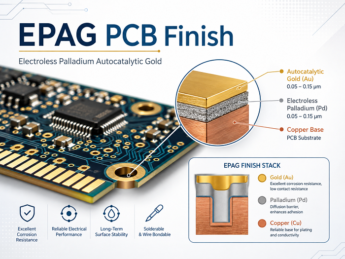
What Is EPAG (Electroless Palladium Autocatalytic Gold)?
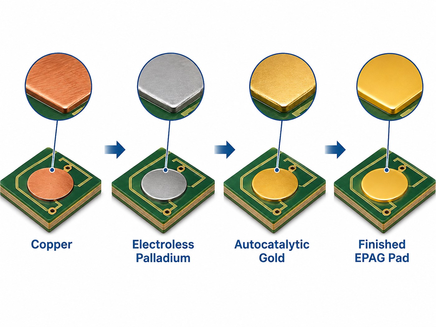
EPAG stands for Electroless Palladium Autocatalytic Gold.
Copper → Electroless Palladium → Autocatalytic Gold
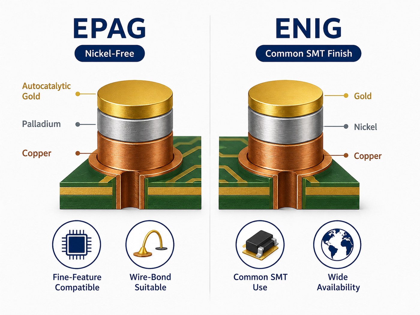
The key difference from ENIG is the absence of electroless nickel. Palladium is deposited over the exposed copper, followed by an autocatalytic gold layer.
This gives EPAG several useful characteristics:
- nickel-free surface construction;
- relatively low metallic buildup around fine features;
- a solderable noble-metal surface;
- compatibility with qualified wire-bonding processes;
- potential advantages in RF and flex designs where nickel is undesirable.
The gold process is also important. Autocatalytic gold can continue depositing after the surface has been covered, which gives more control over functional gold thickness than a conventional immersion-gold process.
For this reason, EPAG should be specified as a complete surface-finish system rather than simply as “palladium gold.”
How Is EPAG Plated on a PCB?
The exact chemistry varies between plating systems, but a typical EPAG plating process follows four main stages.
- Copper preparation: Exposed copper is cleaned and conditioned. Oxides and contaminants must be removed before palladium deposition.
- Electroless palladium plating: Palladium is chemically deposited on the copper without using external electrical current.
- Autocatalytic gold deposition: Gold is chemically reduced onto the palladium surface. Unlike a self-limiting immersion reaction, the process can continue building the gold layer.
- Cleaning and inspection: The board is rinsed and checked for deposit consistency, thickness, solderability, and application-specific requirements.
The process is more specialized than standard ENIG. A PCB manufacturer needs suitable electroless palladium and autocatalytic-gold chemistry, stable bath control, and reliable thickness measurement.
If EPAG is essential to the design, confirm process availability before finalizing the fabrication drawing.
How Does Autocatalytic Gold Differ from Immersion Gold?
The main difference is how the gold layer grows.
Immersion gold relies on a displacement reaction. Gold deposits while a small amount of the underlying metal is displaced. As the surface becomes covered, deposition slows.
Autocatalytic gold uses a chemical reducing agent, so the gold surface can continue supporting further deposition. This makes it easier to build a thicker functional gold layer where required.
| Feature | Immersion Gold | Autocatalytic Gold |
| Deposition method | Displacement reaction | Chemical reduction |
| Deposit growth | Relatively self-limiting | Can continue building |
| Typical role | Protection and solderability | Functional gold surface |
| Thickness flexibility | More limited | Greater |
| Wire-bond use | Process-dependent | More suitable when properly qualified |
For ordinary solder pads, a thin protective gold layer may be sufficient. Wire-bond pads can require tighter control over gold thickness, purity, and surface condition. That is where autocatalytic gold becomes more valuable.
What Are the Advantages of EPAG PCB Finish?
EPAG is most useful when the design benefits from both a nickel-free stack and a controlled gold surface.
- Nickel-free construction: useful when nickel is undesirable for electrical, magnetic, or mechanical reasons.
- Fine-feature compatibility: removing the nickel layer reduces total metal buildup around small pads and tight clearances.
- Wire-bond capability: properly qualified EPAG processes can support gold, silver, or copper wire bonding.
- Solderability: palladium and gold provide a solderable, oxidation-resistant surface.
- RF suitability: removing nickel can be useful on exposed high-frequency conductor areas.
- Flex compatibility: eliminating the relatively hard nickel layer can help in flex designs where finished areas are close to bending zones.
These advantages matter only when they solve an actual design requirement. For a normal SMT control board, they may not justify a more specialized finish.
What Are the Limitations of EPAG Plating?
The first limitation is availability. EPAG is not offered by every PCB manufacturer that provides ENIG or ENEPIG.
Cost can also be higher because the process uses palladium and gold, and some applications require a more substantial gold deposit.
Specification quality is another concern. For critical applications, “EPAG finish” alone may not be enough. A complete requirement may need to define:
- palladium thickness;
- gold thickness;
- solder-only or wire-bond surfaces;
- bonding wire material;
- selective plating areas;
- storage requirements;
- acceptance or qualification criteria.
For a standard SMT board with no RF, bonding, fine-feature, or nickel-related constraint, ENIG may remain the more practical choice.
EPAG vs EPIG: What Is the Difference?
EPAG and EPIG are both nickel-free palladium/gold finishes. The main difference is the gold deposition process.
For more detail on the alternative process, see our EPIG PCB surface finish guide.
| Feature | EPAG | EPIG |
| Full name | Electroless Palladium Autocatalytic Gold | Electroless Palladium Immersion Gold |
| Layer concept | Cu → Pd → autocatalytic Au | Cu → Pd → immersion Au |
| Nickel layer | No | No |
| Gold process | Autocatalytic | Immersion |
| Gold build capability | Greater | More limited |
| Soldering | Suitable | Suitable |
| Wire bonding | Strong option with qualified process | Possible with suitable process |
| Fine-feature use | Suitable | Suitable |
| Main selection reason | Functional gold layer | Nickel-free finish with thinner gold |
EPIG is often sufficient when the main goal is to remove nickel while maintaining a solderable palladium/gold surface. EPAG becomes more attractive when the gold layer itself needs to perform a more demanding function, especially in wire bonding.
EPAG vs ENIG: Which PCB Surface Finish Should You Choose?
For conventional SMT assembly, ENIG is usually the simpler starting point. EPAG becomes relevant when the nickel layer in ENIG creates a specific design concern.
Our ENIG PCB surface finish guide covers the nickel/gold process and its selection limits.
| Selection Factor | EPAG | ENIG |
| Layer structure | Cu/Pd/Au | Cu/Ni/Au |
| Nickel-free | Yes | No |
| Standard SMT | Suitable | Very common |
| Wire bonding | Suitable with qualified process | Not usually the first choice |
| Fine features | Lower metal buildup | Nickel increases total deposit thickness |
| Flex applications | Useful where nickel should be avoided | Application-dependent |
| RF applications | Attractive when nickel loss matters | Common, but contains nickel |
| Availability | Specialized | Widely available |
| Sourcing simplicity | Lower | Higher |
Choose ENIG when you mainly need a flat, solderable, widely supported finish.
Consider an EPAG PCB finish when the project involves:
- exposed high-frequency conductors;
- wire bonding;
- very fine pad geometry;
- repeated flexing near finished areas;
- nickel-sensitive design conditions.
Changing from ENIG to EPAG without one of these reasons usually adds complexity without adding much value.
EPAG vs ENEPIG: What Are the Key Differences?
ENEPIG and EPAG can both support soldering and wire bonding, but their metallic structures are different.
| Feature | EPAG | ENEPIG |
| Layer structure | Cu/Pd/autocatalytic Au | Cu/Ni/Pd/immersion Au |
| Nickel | No | Yes |
| Palladium | Yes | Yes |
| Wire bonding | Suitable | Widely used |
| Soldering | Suitable | Suitable |
| RF consideration | No nickel layer | Nickel remains |
| Flex consideration | Attractive where nickel should be avoided | Nickel layer remains |
| Main selection reason | Nickel-free functional gold | Versatile soldering and bonding |
ENEPIG is already a strong option when one PCB needs both soldering and wire bonding. EPAG should not replace it automatically. The case for EPAG becomes stronger when removing nickel provides a measurable electrical, dimensional, or mechanical benefit.
Is EPAG Suitable for Soldering and Wire Bonding?
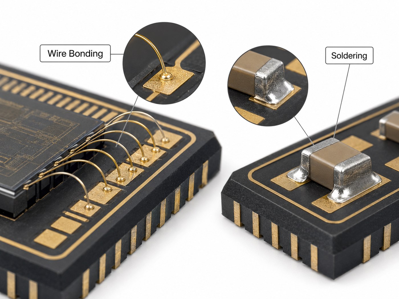
Yes. EPAG can support both, provided the finish is specified and qualified for the intended assembly process.
For deposit-control context, compare the qualification points in our wire bonding EPIG thickness guide.
For soldering, the gold protects the palladium surface before assembly. The finished pad must still meet the solderability requirements of the selected assembly process.
Wire bonding needs tighter control. Important variables include:
- gold thickness and purity;
- surface cleanliness;
- palladium condition;
- bonding wire material;
- wire diameter;
- ball or wedge bonding method;
- bonding force and temperature;
- storage time before assembly.
A surface that looks visually acceptable is not automatically suitable for bonding. For a new production program, prototype bond testing is advisable when the plating chemistry, pad design, bonding wire, or bonding process has changed.
Why Is EPAG Used for High-Frequency and RF PCBs?
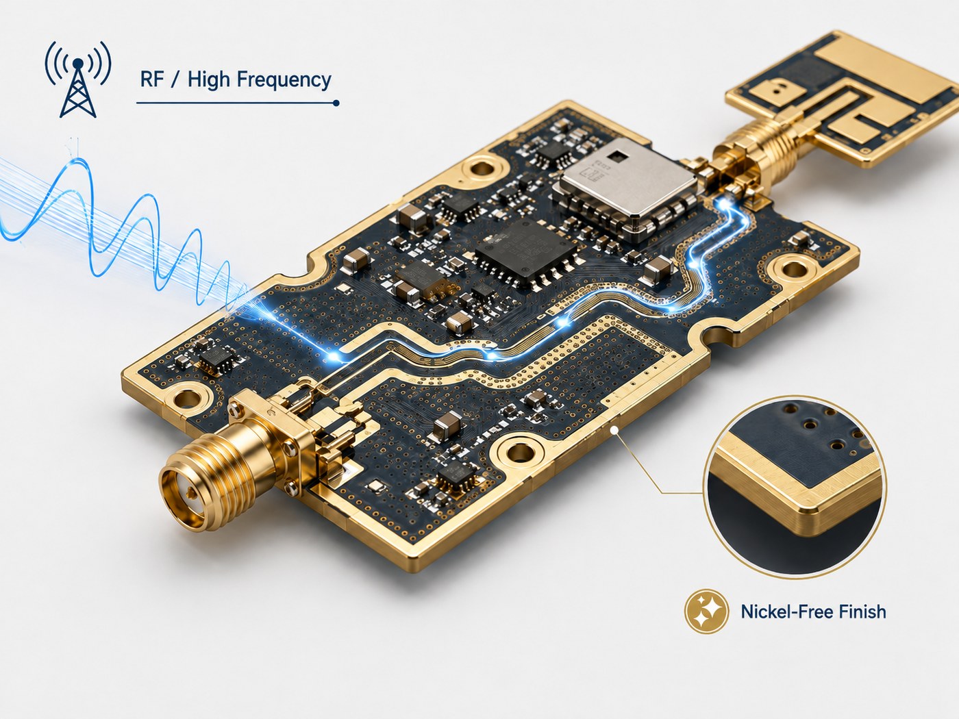
The main RF reason is simple: EPAG removes the nickel layer.
At high frequencies, current becomes concentrated near conductor surfaces because of skin effect. The metallic finish on those surfaces can therefore contribute to conductor loss.
Nickel has much lower conductivity than copper and also has magnetic properties. Removing it from exposed RF conductors can be useful when insertion-loss requirements are tight.
EPAG is worth considering when:
- RF traces or launches contain exposed finished copper;
- operating frequency is high;
- insertion loss is tightly controlled;
- fine RF features make plating buildup important;
- nickel-containing surfaces are undesirable.
However, EPAG is not an automatic RF upgrade.
If most transmission lines remain under solder mask and only small component pads receive surface finish, other factors may have a much greater impact, including:
- copper roughness;
- dielectric loss;
- impedance geometry;
- stackup tolerance;
- connector launches;
- via transitions.
The finish should be selected according to where it actually appears in the RF signal path.
Can EPAG Be Used on Flex, HDI, and Ceramic PCBs?
Yes, but the reason for using EPAG changes with the PCB technology.
Flex PCB
A nickel-free finish can be useful near bending areas because nickel is relatively hard. EPAG may therefore be considered when finished conductors are exposed to repeated flexing.
HDI and fine-line PCB
Removing the nickel layer can reduce total plated buildup around small pads and closely spaced features. This can help preserve finished geometry in dense layouts.
Ceramic PCB
EPAG can also be considered for ceramic substrates, but compatibility depends on the conductor system rather than the ceramic material alone.
Examples include:
- direct-bonded copper ceramic;
- thick-film metallization;
- thin-film metallization;
- plated ceramic substrates.
These constructions may require different preparation and plating routes. Do not specify EPAG for a ceramic board based only on the substrate name. Confirm the exposed conductor metallurgy first.
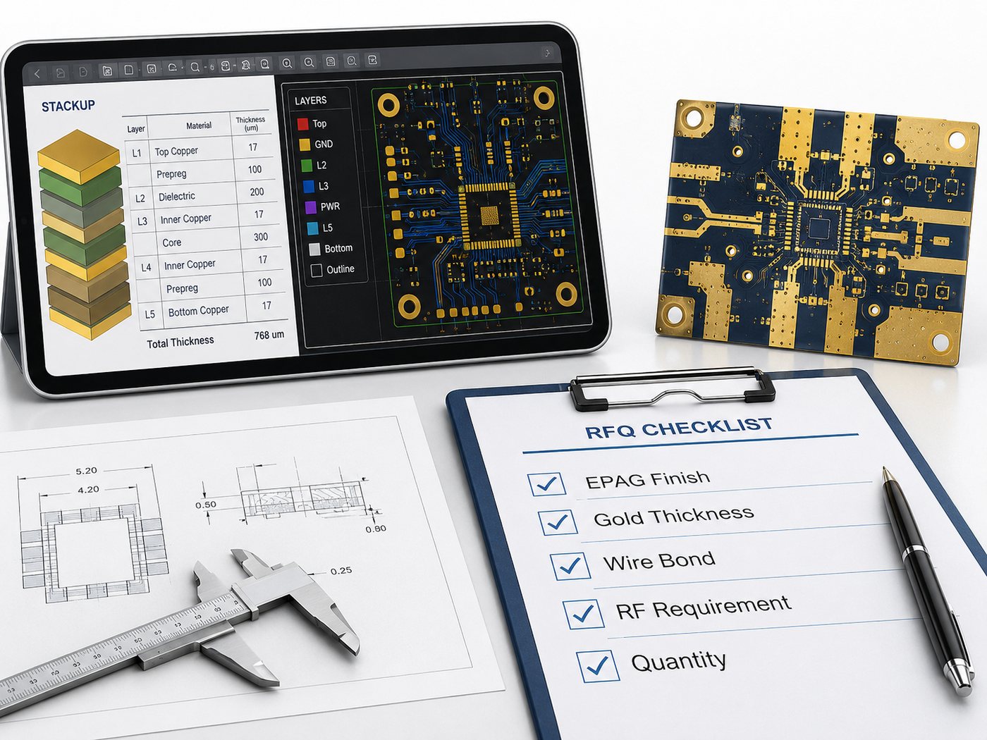
What Should You Specify When Ordering an EPAG PCB?
An EPAG RFQ needs more information than a note saying “gold finish.”
Provide the PCB manufacturer with:
- Surface finish: EPAG / Electroless Palladium Autocatalytic Gold
- Board type: rigid, flex, rigid-flex, HDI, ceramic, etc.
- Base material and stackup
- Board thickness
- Copper weight
- Minimum trace and spacing
- Minimum pad dimensions
- Required palladium thickness, if controlled
- Required gold thickness
- Soldering requirements
- Wire-bond requirements and wire material
- Selective plating areas, if any
- Controlled impedance or RF requirements
- Inspection or qualification standard
- Prototype and production quantities
Avoid copying a plating thickness from an older drawing unless you know why it was specified. Excessive gold can increase cost, while insufficient control can create problems in bonding applications.
At EBest Circuit, we can review the fabrication data, stackup, finish requirement, assembly method, and qualification needs during quotation. We confirm whether the proposed finish route fits the intended soldering, bonding, RF, or flex application before production.
FAQs About EPAG PCB Finish
Is EPAG a nickel-free PCB surface finish?
Yes. EPAG uses electroless palladium over copper followed by autocatalytic gold, without an electroless nickel layer.
What is the difference between EPAG and EPIG?
Both are nickel-free palladium/gold finishes. EPIG uses immersion gold, while EPAG uses autocatalytic gold, which provides greater flexibility for building a functional gold layer.
Can EPAG be used for gold wire bonding?
Yes, provided the plating process, gold thickness, surface condition, and bonding parameters are qualified for the application.
Is EPAG better than ENIG for high-frequency PCBs?
Not always. EPAG can be useful when nickel on exposed RF conductors contributes to loss. If most RF traces are covered by solder mask, material loss, copper roughness, geometry, and connector transitions may matter more.
How should EPAG be specified on a PCB drawing?
Write Electroless Palladium Autocatalytic Gold (EPAG) and add controlled palladium or gold thickness where required. Wire-bond areas, bonding material, selective plating, and qualification requirements should also be identified.
How Can EBest Circuit Review Your EPAG PCB Requirements?
EPAG is valuable when its nickel-free structure and autocatalytic gold layer solve a real bonding, geometry, flex, or RF requirement. For routine SMT boards, a more widely available finish may remain the better purchasing choice.
Send us your Gerber or ODB++ files, stackup, quantity, finish specification, wire material, RF conditions, and deposit or qualification requirements. We will review manufacturability, confirm process availability, and prepare a quotation without assuming that one finish fits every design.