PCB manufacturing PCB manufacturing
Home > Blog

What Is Circuit Board Refurbishing and How Does It Work?

September 2nd, 2026

Electronic equipment can remain useful long after one of its circuit boards begins to age or fail. A damaged relay, degraded capacitor, corroded connector, cracked solder joint, or localized PCB defect does not always justify replacing the complete assembly.

Circuit board refurbishing restores an aged, damaged, or failed electronic board to a usable and verified condition. Depending on the board, the work may involve troubleshooting, cleaning, component replacement, solder rework, conductor repair, and functional testing.

It is particularly relevant to industrial electronics, legacy equipment, discontinued assemblies, and high-value boards where direct replacement may be difficult or uneconomical.

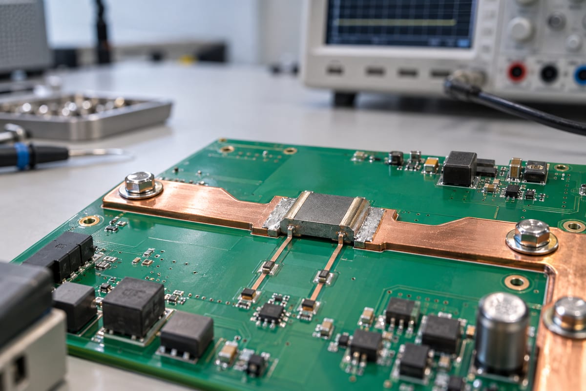
Circuit board refurbishing before and after restoration on an electronics workbench

What Is Circuit Board Refurbishing?

Circuit board refurbishing is a broader restoration process than simply replacing one failed part.

Although the term “circuit board” is sometimes used for a bare PCB, refurbishment usually applies to a populated assembly containing components, connectors, solder joints, and interconnections.

Typical work can include:

  • replacing failed or degraded components;
  • repairing cracked or defective solder joints;
  • restoring damaged pads, traces, or vias;
  • cleaning corrosion and contamination;
  • repairing connectors and contacts;
  • removing and replacing damaged conformal coating;
  • checking areas affected by overheating;
  • testing the board after rework.

The objective is to restore the board to a condition where its required functions can be verified, not to make an old assembly physically identical to a newly manufactured one.

What Is the Difference Between Circuit Board Refurbishing and PCB Repair?

PCB repair normally targets a known fault, while circuit board refurbishing evaluates the board more broadly before returning it to service.

PCB repair compared with circuit board refurbishing
PCB Repair Circuit Board Refurbishing
Usually starts with a specific fault May start with failure, age, or deterioration
Focuses on the failed area Looks at the wider board condition
Often replaces one defective part May replace failed and selected aging parts
Main goal is fault correction Main goal is restoring serviceability
Testing may focus on the repaired circuit Testing may cover a wider range of board functions

For example, replacing a failed relay and checking its output is a repair. If the same board is also inspected for heat damage, deteriorated capacitors, connector corrosion, weak solder joints, and other age-related problems before being functionally tested, the work is closer to refurbishment.

Which Circuit Boards Are Good Candidates for Refurbishing?

Boards are generally worth evaluating when they are expensive, difficult to replace, or installed in equipment that still has useful service life.

Common candidates include:

  • industrial control boards;
  • PLC and automation electronics;
  • motor-drive boards;
  • power-control assemblies;
  • machine-tool electronics;
  • legacy instrumentation;
  • discontinued OEM boards;
  • proprietary low-volume assemblies;
  • equipment with long spare-part lead times.

The best candidates usually have localized faults and a mechanically sound PCB substrate.

Schematics, a BOM, service documentation, firmware information, a known-good board, or an existing test procedure can also make diagnosis much more practical.

What Problems Can Circuit Board Refurbishing Correct?

Refurbishment is most suitable for defects that can be isolated and repaired without rebuilding large portions of the PCB.

Common PCB problems including swollen capacitor, corroded connector, cracked solder joint, burned component, lifted pad and broken trace

Common examples include:

  • high-ESR or failed electrolytic capacitors;
  • worn relays;
  • oxidized or damaged connectors;
  • cracked solder joints;
  • failed MOSFETs, IGBTs, regulators, or diodes;
  • overheated resistors;
  • lifted pads;
  • broken copper traces;
  • damaged plated-through holes;
  • localized corrosion;
  • deteriorated conformal coating;
  • contamination from dust, moisture, or residues.

The visible failure is not always the root cause. A burned MOSFET may have failed because of a damaged gate-drive circuit, excessive load, or another power-stage problem.

Corrosion also needs careful assessment. Surface corrosion near a connector may be manageable, while corrosion beneath packages or inside vias can be much harder to restore reliably.

How Is a Circuit Board Refurbished?

A typical refurbishment process moves from diagnosis to controlled rework and then verification.

Eight-step circuit board refurbishing process from inspection through final testing

1. Review the fault history

Record the board model, symptoms, operating conditions, previous repairs, and when the failure occurs. Intermittent, temperature-related, and load-related faults can point to different failure mechanisms.

2. Inspect the board

Visual and microscopic inspection may reveal:

  • burned components;
  • cracked joints;
  • corrosion;
  • damaged connectors;
  • swollen capacitors;
  • lifted pads;
  • coating damage;
  • previous poor-quality rework.

3. Diagnose the electrical fault

Testing may include continuity checks, resistance measurements, power-rail analysis, signal tracing, diode-mode measurements, and comparison with a known-good board.

4. Clean contaminated areas

Flux residue, dust, oils, and corrosion products may interfere with inspection or electrical performance. Proper cleaning of PCB assemblies after soldering helps technicians expose defects and remove residues. Cleaning materials must be compatible with the PCB, plastics, labels, coatings, and components.

5. Remove defective components

Removal technique depends on the package. A through-hole relay, small resistor, QFN, and BGA each require different tools and thermal control.

6. Repair PCB damage

Localized board restoration may include:

  • pad repair;
  • trace repair;
  • via repair;
  • conductor reinforcement;
  • solder-mask restoration;
  • limited laminate repair.

7. Install replacement parts

Replacement components must match the required electrical ratings, package, polarity, thermal capability, and circuit function.

8. Inspect and test

The reworked area is inspected before the board moves to electrical and functional verification.

Which Components Are Commonly Replaced During Refurbishing?

Components exposed to mechanical wear, heat, or gradual electrical degradation usually receive the most attention.

For basic work, a circuit board repair kit and suitable circuit board repair tools may cover through-hole components, but fine-pitch PCB refurbishment and PCB restoration require controlled heating, inspection, and test equipment.

Frequently evaluated parts include:

  • electrolytic capacitors;
  • relays;
  • connectors;
  • MOSFETs and IGBTs;
  • rectifiers;
  • voltage regulators;
  • optocouplers;
  • heat-stressed resistors;
  • damaged ICs.

Electrolytic capacitors are commonly checked because capacitance, ESR, leakage, and temperature exposure can change over time.

Relays may still actuate mechanically even when their contacts have become resistive or unreliable under load. Connectors can develop similar intermittent faults through oxidation, vibration, or repeated mating cycles.

Parts should not be replaced only because the board is old. Unnecessary rework adds thermal cycles and handling stress to the PCB.

How Are BGA and SMD Components Reworked During PCB Refurbishment?

Fine-pitch SMD and BGA refurbishment requires tighter process control than conventional through-hole repair.

BGA rework station, X-ray inspection and functional testing of a refurbished circuit board

A BGA rework may involve:

  • confirming that the device or solder interface is defective;
  • protecting nearby components;
  • controlling top and bottom heating;
  • removing the package without lifting pads;
  • cleaning and inspecting the land pattern;
  • repairing damaged pads if necessary;
  • reballing or preparing the replacement component;
  • aligning and reflowing the device;
  • inspecting hidden joints by X-ray.

Poor thermal control can warp the PCB, damage laminate, lift pads, or overheat adjacent components.

QFN packages create a similar inspection challenge because part of the solder interface sits beneath the component and cannot be fully checked optically.

How Is a Refurbished Circuit Board Tested?

Testing should confirm that the original fault has been corrected without introducing another defect. A documented PCB inspection step also helps verify workmanship before functional testing.

Depending on the assembly, verification may include:

  • visual and microscopic inspection;
  • continuity and resistance checks;
  • short-circuit checks before power-up;
  • controlled power-up with current limiting;
  • voltage-rail verification;
  • signal and I/O testing;
  • communication testing;
  • relay or actuator operation;
  • functional testing;
  • load testing;
  • X-ray inspection for hidden joints;
  • thermal inspection.

Functional testing is particularly important. Confirming a 5 V rail, for example, does not prove that an industrial controller can read sensors, communicate with another device, drive its outputs, and remain stable under load.

When Is a Circuit Board Not Worth Refurbishing?

Refurbishment becomes difficult to justify when damage is widespread, structural, or impossible to verify after repair.

Warning signs include:

  • severe laminate carbonization;
  • extensive delamination;
  • major internal-layer damage;
  • widespread corrosion;
  • badly damaged BGA pad fields;
  • repeated previous repairs in the same area;
  • large areas affected by overheating;
  • unavailable proprietary ICs;
  • inaccessible firmware or programmed devices;
  • safety-critical boards without an approved repair route;
  • refurbishment cost close to the cost of replacement.

Carbonized PCB material deserves particular caution because it can become electrically conductive. Covering a burned area with coating or epoxy does not necessarily restore its original insulation properties.

Repeated heating can also weaken pads, plated-through holes, and laminate adhesion.

Circuit Board Refurbishing vs Replacement: Which Should You Choose?

Refurbishment usually makes the most sense when the board is valuable, difficult to replace, and affected by a localized fault that can be properly tested afterward.

Situation More Practical Choice
OEM board is discontinued Refurbish
Replacement lead time is long Refurbish
High-value industrial board Evaluate refurbishment
Failure is localized Repair or refurbish
Extensive laminate damage Replace
New board is inexpensive and available Replace
Critical IC is unavailable Replacement may be necessary
Functional testing is impossible Further engineering evaluation
Several areas have repeatedly failed Consider replacement

The comparison should include more than the price of the board. Downtime, machine qualification, software compatibility, installation work, spare-part availability, and equipment lifecycle can materially change the economics.

What Standards Apply to Circuit Board Rework and Refurbishment?

IPC-7711/7721 is one of the main references for electronic assembly rework, modification, and repair. It covers procedures associated with component removal and installation as well as land, conductor, laminate, and coating repair.

Other relevant standards can include:

  • J-STD-001 — requirements for soldered electrical and electronic assemblies;
  • IPC-A-610 — acceptance criteria for electronic assemblies.

The applicable requirement depends on the product, customer specification, assembly class, and industry.

Medical, aerospace, automotive, military, and other controlled applications may impose additional limits on permitted repairs and required documentation.

What Information Should You Provide for Circuit Board Refurbishing?

Clear fault information can reduce diagnostic time and help technicians reproduce the problem.

Useful materials include:

  • photos of both sides of the board;
  • PCB or assembly part number;
  • equipment model;
  • detailed fault symptoms;
  • operating voltage;
  • schematics;
  • BOM;
  • PCB drawings or Gerber files;
  • firmware information;
  • previous repair history;
  • known damaged components;
  • expected I/O behavior;
  • test procedures;
  • a known-good board for comparison.

A description such as “the board does not work” provides little diagnostic value.

A more useful report would be:

“The 24 V input is present, but the 5 V rail falls to 1.8 V after about 20 seconds and U17 becomes unusually hot.”

For intermittent faults, temperature, vibration, load, startup conditions, and operating duration can also help narrow down the cause.

FAQs About Circuit Board Refurbishing

Can an old circuit board be refurbished?

Yes. Older boards can often be refurbished when the PCB remains structurally sound, replacement components are available, and operation can be properly verified after repair.

Can a corroded circuit board be refurbished?

Localized surface corrosion may be repairable. Severe corrosion beneath components, inside vias, or across internal conductors can make restoration much more difficult.

How long can a refurbished circuit board last?

There is no fixed service-life figure. Remaining life depends on the original board condition, component age, operating temperature, electrical load, environment, and quality of the repair.

Is circuit board refurbishing cheaper than replacement?

It often can be for expensive, discontinued, or proprietary assemblies. For low-cost boards that remain readily available, replacement may be more economical.

Can obsolete circuit boards be refurbished?

Yes. Discontinued industrial boards are common refurbishment candidates, although obsolete components, programmed devices, missing documentation, and limited test access can complicate the work.

Can multilayer PCBs and BGA assemblies be refurbished?

Yes, if the damage is repairable and suitable equipment is available. Multilayer conductor damage and hidden-joint packages generally require more specialized rework and inspection than simple component replacement.

What Is the Best Next Step for an Aging Circuit Board?

Start with the board’s fault history, physical condition, replacement availability, and test access. Choose circuit board refurbishment when the defect is localized and the repaired functions can be verified; choose replacement when damage is structural, widespread, or cannot be tested reliably.

You may also like

Hotel Automation PCB Assembly for Smart Hotel Hardware

September 2nd, 2026

Hotel automation PCB assembly provides the hardware foundation for connected, responsive guest rooms. A single project may include room control units, smart thermostats, bedside panels, sensors, relay boards, and gateways—all expected to work together reliably across different room types and repeated installations.

EBest Circuit (Best Technology) supports the stage where approved hotel automation designs become production-ready hardware. From PCB layout and manufacturability review to PCB fabrication, component sourcing, PCBA, and customer-defined testing, we help engineering and purchasing teams move from design data to consistent assembled boards.

hotel automation PCB

What Does a Hotel Automation PCB Control?

A hotel automation PCB connects digital control with the physical functions guests use every day. Depending on the product, it may manage lighting scenes, HVAC signals, curtains, door contacts, occupancy sensing, bedside controls, or do-not-disturb and make-up-room indicators.

Common hardware roles include:

  • A central room controller coordinating lighting, HVAC, and service functions
  • A bedside or wall panel providing local user controls
  • Sensor boards detecting occupancy, temperature, doors, or windows
  • Relay boards switching customer-defined room loads
  • Gateway boards connecting room devices with the hotel room control system

Some hotel automation systems concentrate several functions on one main board. Others use distributed boards connected through wired or wireless interfaces. In both cases, the PCB must support the intended connectors, power domains, communication modules, enclosure, and installation method.

This is why a hotel automation PCB is more than a generic controller board. Its value comes from bringing multiple room functions together in a form that can be installed, identified, serviced, and reproduced across an entire hotel project.

What Must a Hotel Room Control PCB Support?

A hotel room control PCB must balance functionality with practical installation. The board may combine low-voltage control electronics, relays, terminal blocks, sensor inputs, communication modules, and service connectors within a compact enclosure.

A production-ready board should support:

  • Clear separation of control, power, and customer-defined load interfaces
  • Connector positions and orientations suited to field wiring
  • Component heights and mounting features compatible with the enclosure
  • Accessible programming, test, and service connections
  • Controlled hardware options for different room configurations

Consider a guest room control PCB with plug-in field wiring along one edge. If a connector faces away from the enclosure opening, the circuit may be electrically correct while the finished product remains difficult to install. PCB layout and DFM review can help align the approved electrical design with the supplied mechanical requirements before assembly begins.

The same principle applies to hotel room automation variants. Standard rooms and suites may share one base PCB but use different relays, connectors, wireless modules, or component populations. Clear BOMs and board identification make those options easier to manufacture and reorder without confusing one configuration with another.

How Should a Room Control Unit PCB Manage Power and Relays?

A room control unit PCB often places sensitive control electronics close to components that switch lighting, fans, curtains, valves, or other specified loads. Good PCB implementation keeps these functions organized while supporting heat management, isolation, assembly access, and dependable connections.

Once the customer’s relay loads, protection requirements, and isolation strategy are established, the next challenge is carrying them accurately into PCB layout and production.

Important implementation points include:

  • Correct footprints for approved relays, power components, and connectors
  • Suitable copper, spacing, and thermal layout based on customer requirements
  • Practical placement for SMT parts, through-hole relays, and terminal blocks
  • Clear polarity, pin numbering, and assembly information
  • Controlled approval of any proposed component alternative

Relay substitution deserves particular care. Two parts may share a footprint while differing in coil voltage, contact rating, load suitability, dimensions, service life, or approvals. EBest Circuit can identify sourcing constraints and provide alternative-part information, while the customer retains approval of the electrical selection.

By coordinating PCB fabrication, sourcing, SMT assembly, through-hole soldering, and inspection, we help carry the approved power and relay implementation into the finished hardware with fewer handoff gaps.

How Does a Hotel IoT PCB Support Wireless Connectivity?

A hotel IoT PCB connects room hardware with gateways, local networks, or management platforms through a customer-selected wireless technology. Wi-Fi, Bluetooth, Zigbee, Thread, and other modules may support different smart hotel technology architectures.

The wireless module must work as part of the complete board and enclosure—not only as a standalone component.

Consistent wireless hardware depends on:

  • The approved module model and hardware revision
  • Customer-defined antenna keep-out and placement requirements
  • Suitable board outline, connector, cable, and enclosure relationships
  • Controlled programming, provisioning, serial-number, and label instructions

A smart hotel PCB may communicate successfully on the bench but behave differently after installation if wiring, copper, components, or enclosure hardware obstructs the antenna area. With complete customer requirements, PCB layout support can preserve the specified module position and keep-out geometry as the design moves toward fabrication.

Wireless modules may also have long lead times or multiple hardware revisions. If an approved module becomes unavailable or changes revision, EBest Circuit raises the issue before it enters production. This helps later builds remain aligned with firmware references and hardware already deployed in the hotel IoT environment.

hotel automation PCB

What Reliability Checks Matter for 24/7 Hotel Hardware?

Hotel controllers may remain powered around the clock, and the same design may be installed in dozens or hundreds of rooms. Reliability therefore means more than producing one successful prototype. The board must remain consistent across production lots and support practical maintenance or replacement later.

The most important production priorities are:

  • Stable assembly of SMT components, relays, connectors, and terminals
  • Correct component and room-configuration identity
  • Inspection suited to visible and hidden solder joints
  • Functional checks focused on the board’s critical interfaces
  • Revision continuity for repeat orders

The exact controls should follow the assembly. AOI can support SMT inspection, X-ray can verify applicable hidden joints, and focused inspection can address relays or terminal blocks. Customer-defined functional testing may confirm power rails, inputs, communication interfaces, indicators, or relay outputs.

For example, a standard-room board and a suite board may look nearly identical even though the suite version adds relays and uses another wireless module. Clear identification and configuration-specific testing help ensure that the correct board reaches the correct installation.

These controls provide useful production evidence without asking the buyer to manage factory inspection details.

How Is Hotel Room Control PCB Assembly Verified?

Hotel room control PCB assembly verification should confirm that the approved configuration was built and create a reliable reference for repeat production.

A useful first-build handoff provides:

  • The PCB and BOM revisions used for assembly
  • Visibility into approved substitutions and room variants
  • Early findings that may affect fit or repeat production
  • Agreed inspection or functional-test results

The first build may reveal an incorrect footprint, unclear polarity, connector conflict, or inaccessible test point. Resolving these findings before volume production creates a cleaner manufacturing baseline. Our PCB assembly first article inspection checklist can help buyers define this approval stage.

Repeat builds can then follow the approved files, parts, and configuration. Projects that require batch-level records can use our PCB assembly traceability RFQ checklist to define the appropriate evidence before ordering.

hotel automation PCB

Why Choose EBest Circuit for Hotel Automation PCB Assembly?

Hotel automation hardware becomes easier to manage when PCB layout, bare-board fabrication, component sourcing, assembly, and production feedback connect through one manufacturing partner.

EBest Circuit helps buyers move forward with:

  • PCB layout based on approved schematics and mechanical requirements
  • PCB fabrication and PCBA coordinated within one project
  • Sourcing support with customer-controlled substitutions
  • Mixed SMT and through-hole assembly for modules, relays, and connectors
  • Inspection and customer-defined testing matched to the board
  • A consistent manufacturing reference from prototype to repeat orders

Our PCB layout service turns approved circuit, component, interface, and mechanical requirements into production-ready board data. Working alongside the customer’s engineering team keeps the original product intent clear while we focus on manufacturability and execution. Circuit creation, system architecture, firmware, protocol development, certification, and final product approval stay with the customer or its design partner.

For buyers, this creates a focused and accountable path from engineering data to assembled hotel automation hardware—without separately coordinating a PCB supplier, component source, and assembly factory.

Have a room controller, smart thermostat, bedside panel, sensor board, or gateway PCB in development? Send your Gerber files and BOM—or tell us your current project stage—at sales@bestpcbs.com. EBest Circuit will review the manufacturing scope and help define the next step for PCB layout, quotation, or prototype assembly.

FAQs About Hotel Automation PCB

1. What products use a hotel automation PCB?

Hotel automation PCBs are used in room control units, thermostats, lighting and curtain controllers, bedside panels, occupancy sensors, guest-service indicators, relay boards, and hotel IoT gateways. The exact interfaces and assembly requirements depend on the product architecture.

2. Can EBest Circuit provide PCB layout for hotel control hardware?

Yes. We provide PCB layout from customer-approved schematics, component requirements, interfaces, and mechanical constraints. We work alongside the customer’s engineering team while they retain responsibility for the circuit, system architecture, firmware, certification, and final product approval.

3. Can one hotel room control PCB support several room configurations?

Yes, if the product is designed for controlled variants. Different room versions may share one bare PCB while using different relays, connectors, wireless modules, labels, or programming. Clear BOM revisions and configuration-specific testing help prevent production mix-ups.

4. How are wireless modules handled during hotel IoT PCB production?

EBest Circuit can source and assemble the approved module and follow the supplied placement, programming, labeling, and traceability requirements. The customer or design partner provides the antenna, protocol, RF-performance, certification, and final network requirements.

5. What supports consistent hotel room control PCB assembly?

Approved PCB and BOM revisions, controlled substitutions, clear room-variant identification, suitable inspection, and agreed functional testing create a reliable reference for later orders. EBest Circuit coordinates these requirements across PCB fabrication, sourcing, assembly, and repeat production. Contact sales@bestpcbs.com to discuss your project.

You may also like

NRE Cost for PCB: What Is NRE Cost in PCB?

September 2nd, 2026

NRE cost for PCB pays for the project-specific engineering, tooling and production setup that turns your design files into a repeatable manufacturing package. Understanding the charge helps you compare quotations on the same basis, calculate the effective cost per board and plan prototypes, production quantities and repeat orders more accurately.

EBest Circuit (Best Technology) connects DFM review, tooling preparation, PCB fabrication, component sourcing, assembly and testing through self-owned PCB and PCBA factories. Send your Gerber files, fabrication notes, panel requirements and quantities to sales@bestpcbs.com for a quotation that identifies the NRE scope, confirms manufacturing fit and gives you a project-specific lead-time plan.

nre cost for pcb

What Does NRE Stand for in PCB Manufacturing?

NRE stands for non-recurring engineering. In PCB manufacturing and assembly, it refers to project-specific work completed before or around the first production run but not charged as a normal per-board manufacturing operation.

The word “non-recurring” describes the nature of the work, not an unconditional promise that the fee can never appear again. If the approved PCB revision, assembly data, panel, stencil, programming or test requirements remain unchanged, some setup assets may continue to support repeat orders. A significant change can create new engineering or tooling work.

NRE is therefore best viewed as an investment that converts your design data into a controlled production package. Its exact scope depends on whether you are ordering bare PCBs, assembled PCBAs or a broader turnkey service; the next section shows the deliverables that may be included.

What Does an NRE Charge Cover in a PCB Quote?

A useful PCB quotation should connect the NRE charge to identifiable deliverables. The buyer can then see which costs are one-time setup work and which costs apply to every manufactured board.

For bare PCB fabrication, NRE may cover:

  • Gerber or ODB++ data preparation.
  • Stackup, drill and routing-program preparation.
  • Phototools or other process-specific tooling where required.
  • Production panel preparation.
  • Electrical-test programming or dedicated test fixtures.
  • Engineering review for special structures or controlled requirements.

For PCBA, NRE may also cover:

  • Solder-paste stencils.
  • Pick-and-place program preparation from the BOM and CPL.
  • SPI, AOI or X-ray inspection-program setup where applicable.
  • Programming fixtures or procedures.
  • ICT, flying-probe or customer-defined functional-test preparation.
  • Work instructions and first-build setup.

Not every project requires every item. A simple bare PCB, a mixed-technology PCBA and an assembly requiring a custom functional-test fixture should not carry identical NRE scopes. Ask the supplier to identify the deliverable behind each charge rather than presenting NRE as one unexplained amount.

The quotation should also distinguish the sample or first-panel requirement from the requested production quantities. When buyers request several quantity breaks, they can see both the one-time preparation cost and the recurring unit price before selecting the most suitable prototype, pilot or production batch.

nre cost for pcb

How Is NRE Cost Different From PCB Unit Cost?

NRE cost and PCB unit cost answer different purchasing questions.

Cost typeWhat it pays forHow it behaves
NRE costProject-specific engineering, programming, tooling and setupUsually fixed or semi-fixed for the defined revision and scope
PCB unit costMaterial and fabrication for each bare boardChanges with board specifications and quantity
PCBA unit costComponents, placement, soldering, inspection and recurring test workChanges with BOM, assembly complexity and quantity

To compare offers fairly, calculate the effective cost per usable board:

Effective cost per board = recurring unit cost + total NRE ÷ accepted board quantity

This prevents a quotation with a low headline unit price but a high setup charge from appearing automatically cheaper. It also prevents a quotation with NRE included in the unit price from appearing expensive when another supplier lists the same work separately.

The commercial format can vary. One supplier may show every setup item, another may combine them under “tooling,” and another may amortize them into the unit price. The correct comparison is the complete cost for the same files, quantity, inspection scope, test coverage and delivery requirement.

Which PCB Requirements Determine NRE Cost?

NRE is driven by the preparation needed to make your specific design production-ready. Clear input data allows the supplier to define that work more accurately.

The main factors include:

  • PCB complexity: Layer count, controlled impedance, blind or buried vias, rigid-flex construction and special materials can require additional CAM or process preparation.
  • Board and panel format: Finished dimensions, routing, V-scoring, breakaway rails and mixed arrays affect production-panel work and tooling.
  • Assembly complexity: Double-sided assembly, fine-pitch packages, BGA devices, press-fit parts and mixed SMT/THT processes influence stencils, programming and work instructions.
  • Test scope: Standard electrical testing, flying probe, ICT and functional testing require different data, fixtures and preparation.
  • Programming requirements: Firmware loading, device configuration and serial-number handling may need dedicated procedures or fixtures.
  • Documentation requirements: First-article records, traceability, special inspection reports or customer-controlled formats can add project-specific engineering work.
  • Revision readiness: Complete, consistent Gerber, BOM, CPL, drawing and test files reduce clarification and reprogramming.

Complexity should not be removed merely to reduce NRE if it is needed for the product. The better goal is to ensure that every charge supports a necessary production control or deliverable.

How Does Order Quantity Change NRE Cost per PCB?

Order quantity normally does not change the cost of creating one stencil or preparing one machine program as much as it changes how that cost is distributed. The same NRE amount has a larger effect on a small prototype batch and a smaller effect on each board in production.

For illustration, assume that a project has USD 300 of NRE:

Accepted quantityTotal NRENRE allocated per board
10 boardsUSD 300USD 30.00
100 boardsUSD 300USD 3.00
1,000 boardsUSD 300USD 0.30

This example only shows NRE allocation; it does not include recurring PCB, component, assembly, testing or logistics costs.

The practical buying decision is not always “order more.” Engineers may still need a small prototype batch to validate the design. A better approach is to request pricing at the quantities that match your development plan—for example, prototype, pilot and expected production volume. This shows how the same setup investment contributes to the effective cost at each stage.

When several small boards can share a technically suitable production array, PCB panelization may also improve material handling and production efficiency. The array still needs to meet fabrication, assembly and depaneling requirements, so panelization should be reviewed as an engineering decision rather than used only to fill open space.

When Can Repeat Orders Reuse PCB Tooling?

Repeat orders can gain more value from the original NRE investment when the production package remains stable and the supplier can reuse suitable tooling, programs and approved data.

Reuse is more likely when the following remain unchanged:

  • PCB revision and Gerber or ODB++ data.
  • BOM and approved component packages.
  • CPL coordinates, rotation and assembly side.
  • Panel dimensions and breakaway method.
  • Stencil aperture requirements.
  • Inspection and test criteria.
  • Programming files and device configuration.

Confirm what the supplier retains, how long physical tooling is stored and whether it remains suitable for the new order. Stencils and fixtures are reusable only while their condition and production requirements remain compatible. Machine programs may also continue supporting production, while a component-package or coordinate change may require revision and verification.

A stable release package gives both the buyer and supplier a clear reference. Include the PCB revision on purchase orders and confirm that the repeat order uses the previously approved manufacturing data.

nre cost for pcb

How Can You Reduce NRE Costs?

The most effective savings come from making each engineering and tooling activity useful across the intended production path.

  • Release consistent files: Align the Gerber or ODB++ data, BOM, CPL, drawings and test instructions before quotation.
  • Use DFM before tooling: Resolve manufacturability and assembly questions before the stencil, fixture or final machine program is prepared.
  • Define the test purpose: Select test coverage that matches the product and production stage instead of requesting an undefined “full test.”
  • Plan prototype and production quantities together: Ask how the setup package will support the next build if the design is approved.
  • Confirm reusable assets: Identify whether stencils, fixtures and programs can be retained for repeat orders.
  • Control revisions: Give every released dataset a clear revision and communicate changes before production preparation begins.
  • Review panelization early: Confirm array size, rails, fiducials, tooling holes and depaneling before the panel becomes part of the production package.

For early-stage products, prototype PCB assembly can validate the release package before a larger quantity is authorized. This keeps the initial engineering and tooling investment useful as the project moves from prototype to repeat production.

What Should an NRE Fee Show in a PCB Quote?

A buyer-friendly quote makes the one-time work easy to understand and easy to compare.

Request confirmation of:

  • The NRE item and its production purpose.
  • The approved revision and input files on which the quote is based.
  • Whether the charge includes a stencil, fixture, programming, test preparation or other engineering setup.
  • Unit prices for the sample, pilot and planned production quantities.
  • Which tools, programs and approved data can support repeat orders.
  • The changes or tooling conditions that would require additional NRE.
  • Whether NRE is separate from or included in the recurring unit price.
  • When the quoted lead time begins and whether it includes tooling and first-build approval.
  • Whether the supplier's proven PCB or PCBA capabilities match the project.

When comparing suppliers, keep the scope constant. A quotation that includes a test fixture, first-build documentation and controlled traceability is not directly comparable with one that includes only basic board fabrication. The clearer quote is often more useful because it shows what will be ready before production and what evidence or tooling will remain available afterward.

What NRE Engineering Support Does EBest Provide?

EBest helps customers turn one-time engineering and tooling costs into a production package that can support prototypes, approval builds and repeat orders.

  • A clearer production package: One business contact works with three engineering specialists to review Gerber files, BOMs, CPLs, panel requirements and test instructions before tooling is released. You can see which NRE items create stencils, programs, fixtures or manufacturing data that may support future orders.
  • One production path: Our self-owned PCB and PCBA factories connect fabrication, component sourcing, SMT or through-hole assembly, inspection and testing. Approved data and tooling can move from prototype validation into production without transferring the project between unrelated suppliers.
  • Controlled repeat production: ISO 9001, ISO 13485, IATF 16949 and AS9100D quality systems support different project requirements. MES traceability connects approved revisions with material batches, production records and finished products.

Lead time is confirmed with the NRE scope because tooling, programming and test preparation can affect the production start date. For standard FR-4 prototypes under one square meter, normal lead time is typically 7–12 days depending on layer count, with expedited options from 24–72 hours. Standard PCBA projects can generally be planned around one week, while urgent quick-turn PCBA may be reviewed for service as fast as two days when files, components and test requirements are ready. Final timing is confirmed against the actual project rather than treated as an automatic commitment.

Send the current Gerber or ODB++ files, fabrication drawing, panel requirement, revision and planned quantities. For PCBA, also include the BOM, CPL, assembly drawing, programming files and test requirements. EBest can then identify the one-time preparation, reusable production assets and recurring production scope for your quotation.

nre cost for pcb

FAQs About NRE Cost for PCB

What does NRE stand for in PCB manufacturing?

NRE stands for non-recurring engineering. It covers project-specific preparation such as engineering review, CAM work, tooling, stencils, machine programming or test-fixture preparation before or around production.

Is PCB NRE paid only once?

It is generally associated with one defined design revision and production scope. Suitable tools and programs may support repeat orders, but design changes, new test requirements, worn tooling or supplier retention policies can create additional work.

Why does NRE have a larger effect on prototype pricing?

The fixed setup amount is distributed across fewer boards. The same NRE allocated across a production quantity contributes much less to the effective cost of each board.

Does a larger order always reduce the total NRE charge?

Not necessarily. A larger order usually reduces the NRE allocated per board, while the total setup charge may remain similar. Additional panels, fixtures or production requirements can change the total scope.

Can a PCB supplier remove the NRE fee?

A supplier may include NRE in the unit price, discount part of it or reuse existing tooling, but the underlying preparation still has a cost. Compare the complete project total and included deliverables rather than judging the quote only by whether an NRE line is visible.

Send your current PCB or PCBA data to sales@bestpcbs.com for a quotation that separates project-specific preparation from recurring production costs. EBest Circuit will review the files, quantity, assembly scope and test requirements so you can see what the initial setup supports and how it fits your prototype and production plan. Start with a clear review of your NRE cost for PCB.

You may also like

RGB LED Board: Circuit, Power, Layout, and Manufacturing Guide

September 2nd, 2026

An RGB LED Board combines red, green, and blue light channels on one PCB so a controller can mix colors, dim the output, and create visual effects. Reliable performance depends less on the number of colors than on the chosen LED architecture, current control, voltage-drop margin, heat removal, and production test plan.

This guide focuses on the engineering decisions that separate a stable board from one that flickers, shifts color, overheats, or fails at the end of a long power path. It covers discrete and addressable LEDs, 5V and 12V systems, PCB layout, assembly, inspection, and the information needed for a realistic manufacturing quote.

RGB LED Board with an array of red, green, and blue LEDs, controller IC, connectors, and copper routing

What Is an RGB LED Board?

An RGB LED board is a printed circuit assembly that controls three light-emitting channels to produce a wide range of colors. The channels may be separate dies inside one package, independent high-power LEDs, or addressable pixels with an integrated control IC.

The term can describe a small indicator board, an illuminated human-machine interface, a decorative strip, a matrix panel, or a high-output lighting module. That range matters because a compact indicator and a large display do not share the same current, thermal, routing, or test requirements.

How Does an RGB LED Board Display Work?

An RGB LED Board Display creates color by changing the relative intensity of the red, green, and blue channels. Conventional circuits use three current-controlled outputs per LED, while addressable pixels receive serial data and generate their own channel PWM internally.

The visual result depends on more than digital color values. LED binning, forward-voltage variation, driver accuracy, PWM resolution, refresh rate, diffuser geometry, ambient light, and board temperature can all change perceived brightness or color uniformity.

Architecture Control Method Best Fit Main Design Constraint
Discrete RGB LED Three resistors or constant-current channels Indicators and simple color status Channel current and common-anode/cathode selection
Matrix with external driver Multiplexing or multi-channel constant-current IC Displays and uniform animation Refresh rate, row current, and driver heat
Addressable RGB pixel Serial data passed from pixel to pixel Effects, signs, and modular lighting Power distribution, data margin, and failure propagation
High-power RGB module Dedicated constant-current drivers Architectural and high-output lighting Thermal path, current matching, and optics

RGB LED Board 5V or RGB LED Board 12V: Which Should You Choose?

Choose 5V when the LED package or driver requires it and the board can support the resulting current; choose 12V when the selected LED architecture is designed for 12V and lower distribution current is important. Voltage is not interchangeable, so the LED and driver datasheets must define the final rail.

For equal electrical power, a 12V feed carries less current than a 5V feed, which reduces connector and trace loss. However, many 12V addressable products group LEDs or use internal regulation, changing pixel granularity and efficiency. A 5V board may offer finer pixel control but need wider copper, more injection points, and stronger connectors.

Comparison of 5V and 12V RGB LED board power distribution architectures
Decision Point 5V Board 12V Board
Distribution current at equal power Higher Lower
Typical control granularity Often one addressable LED package May control grouped LEDs, depending on the part
Power-path priority Wide copper and frequent injection Input protection and local voltage conversion where needed
Selection rule Use only the voltage and topology specified for the selected LED and driver

For a practical 5V addressable example, see our guide to a rigid 5V addressable RGB strip.

How Should Power and Current Be Calculated?

Calculate the worst-case current from the LED or driver datasheet, then verify copper loss, connector rating, supply margin, and temperature at the intended duty cycle. For addressable pixels, a conservative first estimate is the pixel count multiplied by the maximum full-white current per pixel; the validated design should use the actual selected part.

Older 5V addressable pixels are sometimes budgeted at up to 60mA each at full white, but newer devices can differ substantially. Do not copy that value into a production specification without checking the exact package. The same caution applies to brightness-limited firmware: software limits are useful, but the hardware should still fail safely.

  • Estimate worst-case LED, driver, regulator, and controller current.
  • Calculate path drop with ΔV = I × R for traces, vias, cables, and connectors.
  • Check the lowest voltage at the farthest LED under maximum load.
  • Provide bulk capacitance at the input and local decoupling near switching loads.
  • Add power-injection points when one feed cannot hold the voltage window.
  • Measure full-white current and board temperature on the assembled prototype.
RGB LED board power layout showing wide power paths, bulk capacitance, local decoupling, and test points

How Should the Driver and Control Interface Be Selected?

Select the driver from the required channel count, current accuracy, PWM resolution, refresh behavior, communication interface, and thermal limit. A simple indicator may need three transistor or current-sink channels, while a matrix may benefit from an I2C or SPI constant-current driver with independent color and brightness control.

RGB dimming usually uses three PWM channels. Dedicated RGB drivers can add current matching, phase-shifted PWM, fault reporting, and lower microcontroller workload. Addressable LEDs reduce driver count but make logic thresholds, data timing, chain length, and power sequencing part of the board-level design.

A 3.3V controller does not automatically provide a reliable logic-high level to every 5V pixel. Verify the input threshold across supply and temperature, and add a logic-level shifter when the noise margin is insufficient. For many addressable designs, a 300–500Ω series resistor close to the first data input and a 500–1000µF bulk capacitor near the power entry are useful starting practices, subject to the selected device guidance.

Which PCB Layout Rules Improve Color Stability and EMC?

Stable color requires low-impedance power and ground paths, controlled switching loops, short data routes, and consistent local decoupling. A board can pass a low-brightness bench test yet flicker at full white when return-path voltage or simultaneous switching noise shifts the logic reference.

  • Use continuous ground where possible and avoid routing data across return-path gaps.
  • Place the driver, level shifter, and input protection close to the signals they serve.
  • Keep each decoupling capacitor close to its LED or driver power pins.
  • Use copper pours, parallel feeds, and sufficient vias for high-current distribution.
  • Separate noisy switching nodes from sensitive data, clock, and analog reference paths.
  • Add accessible test points for input power, ground, data, clock, and key driver rails.

For broader component placement and routing context, our earlier RGB LED PCB design article provides a useful starting reference.

How Should Heat Be Managed?

Manage heat by converting LED and driver losses into a realistic power map, then giving that heat a low-resistance path into copper, the enclosure, airflow, or a heat-spreading substrate. RGB boards can heat unevenly because the three color dies have different forward voltages and because animation does not load every channel equally.

FR-4 is appropriate for many indicators, decorative modules, and moderate-power displays. High-output lighting may need thicker copper, thermal vias, a metal-backed board, interface material, or an enclosure heat sink. The choice should follow measured junction or board temperature rather than an automatic material rule.

When the LED power density is high, review the thermal options in our LED PCB manufacturing and thermal design guide.

What Manufacturing and Assembly Checks Matter?

Manufacturing control should protect LED orientation, solder quality, optical uniformity, and the high-current power path. RGB packages can look symmetrical while having a strict pin-one or data-direction requirement, so assembly drawings and silkscreen must make orientation unambiguous.

  • Confirm LED polarity, pin-one, data-in/data-out direction, and common-anode or common-cathode selection.
  • Review stencil apertures for exposed pads, thermal pads, and fine-pitch driver packages.
  • Control board flatness when lenses, diffusers, or light guides need consistent spacing.
  • Use AOI for component presence, orientation, and solder-joint screening.
  • Use X-ray where a hidden thermal pad, QFN, BGA, or bottom-terminated joint requires it.
  • Protect LED optical surfaces from contamination, scratches, and incompatible cleaning residues.
Engineer inspecting assembled RGB LED boards and running a red, green, and blue functional test

A complete LED module assembly process should connect PCB inspection with optical and functional verification rather than treating solder quality as the only acceptance criterion.

How Should an RGB LED Board Be Tested?

Test each color channel independently before running mixed-color patterns, then repeat the test at the lowest and highest specified input voltage. This sequence separates assembly defects from firmware, color-order, power-distribution, and thermal problems.

  1. Inspect orientation, solder joints, bridges, contamination, and damaged LED packages.
  2. Check resistance or current-limited power-up before applying full supply current.
  3. Light red, green, and blue separately to detect swapped or open channels.
  4. Run black, primary colors, white, gradients, and fast transitions.
  5. Measure input current, far-end voltage, connector rise, and hot spots at maximum intended duty.
  6. Test communication margin, startup behavior, reset behavior, and power-cycle recovery.
  7. Use a fixture or camera method when brightness and color uniformity are acceptance requirements.

The functional test specification should define allowable dead pixels, channel failures, brightness variation, current limits, and cosmetic defects. A vague instruction such as “lights OK” is not repeatable enough for production.

What Affects RGB LED Board Price?

RGB LED Board Price is driven mainly by LED count and grade, driver complexity, PCB size and copper, assembly density, thermal structure, optical requirements, and functional test coverage. A low-cost board can become expensive if color uniformity, high brightness, waterproofing, tight binning, or individual-pixel testing is added late.

Cost Driver Why It Changes Cost
LED type and binning Affects component price, color consistency, brightness, and sourcing risk
Board area and copper Changes material use, current capacity, panel utilization, and thermal behavior
Driver and control circuit Adds ICs, passives, programming, routing density, and validation effort
Assembly and inspection Depends on package pitch, bottom-terminated joints, AOI, X-ray, and rework access
Functional and optical test Fixture time and acceptance criteria increase with pixel count and uniformity requirements

For a useful comparison, send the same controlled file set to each manufacturer. Otherwise, one quote may include programmed parts, optical testing, or cable assembly while another covers only bare PCB fabrication.

FAQ About RGB LED Boards

Can a 3.3V microcontroller control a 5V RGB LED board?
It can when the LED or driver recognizes the 3.3V logic-high level under all operating conditions. Many 5V addressable LEDs need a logic-level shifter for reliable margin, so the component datasheet and worst-case voltage thresholds should decide the interface.
Does every RGB LED need a resistor?
Discrete RGB LEDs normally need current limiting for each color channel unless a constant-current driver provides it. Addressable RGB packages usually integrate their own driver, but they still need correct local decoupling and may need a series resistor on the incoming data line.
Why does an RGB LED board show the wrong color?
Wrong color usually comes from an incorrect channel order, a common-anode versus common-cathode mismatch, weak ground reference, voltage drop, a damaged channel, or the wrong data protocol. Testing red, green, and blue separately helps isolate the fault.
Is FR-4 suitable for an RGB LED board?
FR-4 is suitable for indicators, decorative panels, and many moderate-power RGB assemblies when copper area and airflow control temperature. High-power or tightly enclosed lighting may need a metal-core PCB or another thermal path after a verified thermal analysis.
What files are needed to quote a custom RGB LED board?
A useful quote package includes Gerber and drill files, BOM, pick-and-place data, assembly drawings, LED and driver datasheets, input voltage, LED count, dimensions, quantities, color or brightness requirements, and the required functional test.

How Can EBest Circuit Support Your RGB LED Board Project?

At EBest Circuit, we support PCB design review, prototype fabrication, component sourcing, PCB assembly, AOI, X-ray where applicable, and functional testing for custom LED electronics. We can review the power path, LED orientation, driver package, thermal structure, panelization, assembly data, and production test requirements before volume build.

Send your Gerber files, BOM, pick-and-place data, LED and driver datasheets, input voltage, dimensions, quantity, and test requirements to sales@bestpcbs.com. We will use that information to prepare a manufacturing review and quotation for your RGB LED Board.

You may also like

Metal Core PCB Manufacturers in Spain: Companies, Capabilities and Sourcing Options

September 2nd, 2026

Metal Core PCB manufacturers in Spain include CIRLAN, Fast PCB, Maxwell Atlantic and CIPSA Circuits. The useful differences are practical: which IMS structures they describe, what quality controls they disclose, whether they publish a lead time, and whether they supply only bare boards or can cover a wider manufacturing scope.

If you are sourcing an aluminium or copper-base PCB, start with the structure and delivery requirement. A single-sided lighting board, a double-sided PTH IMS design and a fully assembled thermal board do not belong in the same RFQ. The comparison below shows what each supplier publicly offers and which details still need a written quotation.

Metal Core PCB manufacturers in Spain, aluminium and copper IMS panels in a quality inspection lab

Who Are the Main Metal Core PCB Manufacturers in Spain?

CIRLAN, Fast PCB, Maxwell Atlantic and CIPSA Circuits all identify finished PCB manufacturing operations in Spain and publish an IMS or metal-core offer. Their process scope and delivery visibility are not the same.

Company Process capability Lead-time information Service scope
CIRLAN
Urnieta, Gipuzkoa
Single-sided aluminium and copper IMS; published standard and special dimensional ranges No standard IMS turnaround published; factory route and committed date belong in the quote Engineering, optimisation, panelisation and bare PCB manufacturing; some technologies may use Shenzhen partners
Fast PCB
Irún, Gipuzkoa
Single-sided aluminium IMS; 0.8–3.2 mm base, 35–105 µm copper and 100 m²/day stated capacity Short series: 5 working days
Large series: 10 working days
Bare PCB prototypes and series; routing, V-scoring, chemical tin and optional production certificate
Maxwell Atlantic
Santiago de Compostela
Aluminium or copper IMS within an in-house single-, double- and multilayer PCB process No standard IMS turnaround published; ask for prototype and repeat-order dates separately Bare PCB manufacturing for prototypes and small, medium or large series; in-house inspection and traceability
CIPSA Circuits
Rubí, Barcelona
Aluminium IMS, including single-sided, isolated-hole, double-sided and PTH structures General PCB prototype service: 24 hours to 5 days; confirm that the quoted IMS build qualifies Bare PCB prototypes and series with process testing and lot traceability

Match the shortlist to the actual build before requesting prices. Fast PCB publishes defined timing for single-sided aluminium IMS; CIRLAN provides aluminium and copper single-sided process limits; CIPSA documents double-sided and PTH aluminium structures; and Maxwell Atlantic offers broad in-house PCB inspection and traceability. Send the same material, quantity, test, dispatch-date and delivery-price requirements to the relevant suppliers so their quotations cover the same work.

CIRLAN

CIRLAN publishes one of the clearest Spanish process windows for single-sided aluminium and copper IMS. Its aluminium range lists 1.0, 1.5, 2.0 and 3.0 mm board thicknesses. Standard copper is 35 or 70 µm; 105 µm is listed as special production. The same table gives track and spacing, drill, routing, scoring, panel-size and finish limits.

That detail helps a buyer see whether a conventional IMS design falls inside the standard column before requesting a quote. It does not publish a standard turnaround or price. Ask CIRLAN to identify the dielectric grade, thermal data, metal alloy, inspection package and dispatch date for the released files.

CIRLAN separates local services from outsourced technologies. Its local scope includes engineering, optimisation, panelisation, aluminium IMS and copper IMS. The company also describes cooperation with PCB factories in Shenzhen for other technologies. If Spain production is a purchasing condition, the quotation should name the physical plant for the exact part.

Fast PCB

Fast PCB is the easiest supplier in this group to assess when the project is a conventional single-sided aluminium board and delivery speed matters. Its IMS page states 5 working days for short series, 10 working days for large series and 100 m²/day of production capacity.

The published process range covers aluminium bases from 0.8 to 3.2 mm, copper from 35 to 105 µm, a maximum delivery format of 544 × 390 mm, chemical tin, CNC routing and V-scoring. That is enough to reject obvious mismatches before engineering spends time on an RFQ.

Fast PCB also describes a metallographic laboratory that performs ageing tests, thermal shock, digital microsection measurement and solderability checks. A production certificate can be supplied with the order on request. Put the required report, sampling level and acceptance criteria into the purchase specification; do not assume every report is included in the unit price.

Its public IMS offer is specifically single-sided aluminium. Copper-base, plated-through-hole, double-sided IMS and alternative finishes need an explicit technical answer and separate schedule.

Maxwell Atlantic

Maxwell Atlantic is relevant when a buyer wants broad in-house PCB process control as well as an aluminium or copper IMS option. The Santiago de Compostela company states that its PCB manufacturing is carried out without third-party subcontracting and can cover prototypes plus small, medium and large series.

Its listed equipment and processes include CNC drilling and milling, lamination, single-, double- and multilayer etching, electroplating, desmear, AOI, solder-mask processing, laser marking and flying-probe electrical test. The quality system follows UNE-EN-ISO 9001, and the company describes full traceability for raw materials and test results.

This is useful quality evidence, but the public pages do not provide an IMS-specific lead-time table or detailed metal-core process window. The quotation should therefore state the exact IMS structure, dielectric, thermal and isolation values, PTH method, inspection reports, quantity break and committed dispatch date. Ask for the IMS limits, not a general PCB capability list.

CIPSA Circuits

CIPSA Circuits publishes the widest aluminium IMS structure range among the four companies compared here. Its capability material covers single-sided boards, isolated holes, openings in the aluminium, double-sided PTH with an aluminium base and double-sided constructions with an aluminium core. Several structures list 35 or 70 µm copper and 0.15 mm line and spacing.

CIPSA states on its quality page that it performs rigorous controls throughout manufacturing and retains traceability for raw materials and test results. Its general prototype service runs from 24 hours to 5 days and uses the same production lines and finishes as series manufacture. Because that timing page covers PCB prototypes broadly, ask CIPSA to confirm whether the actual IMS material and construction qualify for the requested expedite window.

CIPSA is a strong technical candidate for aluminium IMS that goes beyond a basic single-sided board. Copper-core IMS, the current revision of the capability data, inspection deliverables, setup charges and freight to the final destination still need to appear in the quotation.

How Do These Metal Core PCB Manufacturers Compare?

Do not compare four unit prices until every quote covers the same material, tests, quantity, delivery point and service scope. A cheaper line item can become the expensive choice once tooling, certificates, freight or a second supplier for assembly is added.

Buyer concern What to compare What the quote should state
Quality IMS material identity, electrical test, isolation test, dimensional inspection, traceability and non-conformance handling Named material and factory, test method, sampling or 100% scope, reports supplied and acceptance criteria
Total price Unit price at prototype and repeat quantities, tooling, test reports, special material, packing, freight and import charges Separate line items, quotation validity, quantity breaks, Incoterm and currency
Lead time DFM response, material procurement, fabrication, test, packing and transit Clock start, working days, engineering-hold rule, dispatch date and arrival responsibility
Service scope Bare PCB only or PCB plus component sourcing, assembly, inspection, functional test and shipping Exact owner for each stage, included deliverables and warranty or failure-analysis route

Ask for two dates: the factory dispatch date and the expected delivery date at your site. A five-day fabrication promise is not a five-day delivered order if material approval, engineering questions or freight sit outside the quoted clock.

What Should You Check Before Choosing a Metal Core PCB Manufacturer?

Approve the complete thermal and commercial build, not just an “aluminium PCB” label. These checks prevent the most common gaps between an attractive quotation and the board that actually arrives.

  • Lock the thermal stack: name the IMS material, metal alloy, dielectric thickness, dielectric performance, finished copper and total board thickness. Ask whether the thermal value is typical or guaranteed.
  • Define electrical isolation: specify working voltage, test voltage, dwell time and acceptance limit. For PTH IMS, require the supplier to show how barrels and pads are isolated from the metal.
  • Control the mechanical interface: include outline, flatness, hole and slot tolerances, burr limits, countersinks, V-score and the heat-sink contact surface.
  • Check repeatability: ask which material and factory will be used for prototypes and series. Any material or site substitution should need written approval.
  • Match the inspection to the risk: define electrical test, isolation test, dimensional report, material certificate, first-article check and lot traceability. State which documents must ship with the boards.
  • Close the delivery assumptions: agree when the clock starts, what pauses it, which parts of the schedule are expedited and whether the promised date is dispatch or arrival.

For a pilot order, keep the supplier’s deviations list with the approved files. When the board moves into repeat production, compare the new material lot, factory, process and test plan against that record before release.

Metal Core PCB manufacturers in Spain, IMS stackup and quality checks before supplier approval

EBest Circuit – An Overseas Metal Core PCB Manufacturing Option for Spain

If the project does not require Spain-local fabrication, EBest Circuit can combine metal-core PCB fabrication, component sourcing, PCBA, inspection and testing under one order. That removes the handoff between a bare-board factory, a component buyer and an assembly house. One team reviews the Gerber or ODB++, stackup, BOM, placement data and test requirements before production.

For standard MCPCB prototypes below 1 m² using standard aluminium, 0.8–2.0 mm board thickness, H/H or 2 oz copper, lead-free HASL, white solder mask, black legend and 0.8 W/(m·K) material, EBest publishes these manufacturing references:

  • Single-layer MCPCB: 4 days standard, with a 24-hour fastest option;
  • Two-layer MCPCB: 14 days standard, with a 168-hour fastest option;
  • Four-layer MCPCB: 21 days standard; expedite timing is reviewed per design.

Copper-base, higher-conductivity, heavy-copper, special-finish, multilayer or custom-test builds need a project schedule. For full PCBA, the standard published reference is 10–12 business days from confirmed files and purchase order, subject to BOM availability and test scope.

The commercial advantage is a quote that can show the complete delivered scope: bare board, components, SMT or THT assembly, AOI, functional test, packing and freight to Spain. This makes the total cost easier to compare with a local bare-board quotation. EBest also provides a free DFM review, so material, isolation, panelisation and assembly risks can be raised before the order is released.

Use the same drawings, quantities and quality requirements when comparing EBest with Metal Core PCB manufacturers in Spain. Then compare the final delivered price and arrival date rather than bare-board price alone.

What Should You Include in a Metal Core PCB RFQ?

A complete RFQ reduces both price padding and schedule surprises. Send the same controlled package to every supplier:

  • Gerber or ODB++, drill files and revision-controlled fabrication drawing;
  • metal type and alloy, dielectric, finished copper and total thickness;
  • required thermal and electrical-isolation performance;
  • outline, slots, holes, countersinks, flatness, burr and V-score limits;
  • surface finish, solder mask, legend, panelisation and breakaway method;
  • electrical, isolation, dimensional and traceability deliverables;
  • prototype, pilot and repeat quantities, plus annual demand;
  • requested factory dispatch date, delivery address and Incoterm;
  • BOM, approved alternates, CPL, assembly drawing and test specification when PCBA is required.

Require the quotation to list deviations and exclusions beside the price. If the supplier proposes a different dielectric, omits a test or starts lead time only after a later approval, you should see that before comparing totals.

Metal Core PCB manufacturers in Spain, quality evidence and RFQ documents checked before ordering

FAQs About Metal Core PCB Manufacturers in Spain

Q1: Which Spanish supplier publishes a lead time for aluminium IMS?

A1: Fast PCB states 5 working days for short series and 10 working days for large series. CIPSA publishes a broader PCB prototype service of 24 hours to 5 days, but the requested IMS construction should be confirmed for that service.

Q2: Which companies publish copper IMS capability?

A2: CIRLAN and Maxwell Atlantic list copper as well as aluminium IMS. The quote should still identify the copper base, dielectric, factory and process limits for the part.

Q3: Which supplier publishes double-sided or PTH IMS structures?

A3: CIPSA publishes aluminium IMS options that include double-sided and PTH constructions. Ask for the current capability revision and the isolation method around plated features.

Q4: How should I compare metal core PCB prices?

A4: Compare the same material, quantity, tooling, tests, reports, packing, freight and delivery term. Separate bare-board and PCBA costs so missing work does not make one quote look artificially low.

Q5: What quality records should I request?

A5: Typical records include material identity, electrical-test results, isolation-test results, dimensional inspection, lot traceability and any agreed first-article report. Put required documents in the purchase order.

Q6: Does a short fabrication lead time include delivery to Spain?

A6: Usually not unless the quotation says so. Ask for the clock start, fabrication days, dispatch date, freight method and expected arrival date.

Q7: Can one supplier handle both metal-core PCB and assembly?

A7: Some overseas suppliers, including EBest Circuit, offer metal-core PCB fabrication, component sourcing, PCBA and testing together. The Spanish suppliers reviewed here mainly present bare PCB manufacturing services.

Q8: What files are needed for an accurate quotation?

A8: Send Gerber or ODB++, drills, stackup, fabrication drawing, thermal and isolation requirements, quantity and delivery target. Add BOM, CPL, assembly drawing and test instructions for PCBA.

Conclusion

The best supplier depends on the exact structure and delivery model. CIRLAN publishes detailed single-sided aluminium and copper IMS limits. Fast PCB provides the clearest stated series lead times for single-sided aluminium. Maxwell Atlantic offers broad in-house PCB processing and traceability. CIPSA publishes aluminium IMS structures that include double-sided and PTH options.

Compare quality evidence, total delivered cost, clock start, dispatch date and service scope before choosing. If you need a combined metal-core PCB and PCBA route for delivery to Spain, send Gerber or ODB++, stackup, quantities, BOM, CPL, assembly drawing, test requirements and target arrival date to sales@bestpcbs.com. EBest Circuit will provide a free DFM review and a project-specific quotation.

You may also like

Electronic Glass Cloth Price Increase 2026: PCB Cost and Lead-Time Impact

September 2nd, 2026

electronic glass cloth moved from a background laminate input to a visible PCB supply-chain issue in 2026. A June supplier notice reported increases of 30% for E-glass cloth and 15% for FLD2 cloth, while an August 28 notice reproduced by industry media reported a 20% adjustment for thin-cloth prepreg below 7628, versus 10% for FR-4 and the notice’s 7628-and-above prepreg group.

These figures do not mean every PCB quotation rises by the same percentage. They show where material pressure is building. The effect on a finished board depends on the laminate system, glass style, resin content, layer count, panel utilization, supplier stock, yield, order quantity, and required delivery date.

Electronic glass cloth used in FR-4 laminate, prepreg, and multilayer PCB manufacturing

What Is Electronic Glass Cloth in a PCB?

Electronic-grade woven glass fiber fabric is made from fine glass yarn woven into a controlled cloth. Laminate manufacturers combine it with epoxy, polyimide, or another resin system to make rigid cores and prepreg. In an FR-4 construction, the woven reinforcement contributes electrical insulation, dimensional stability, heat resistance, and mechanical strength.

Several terms appear in specifications and searches. They overlap, but they are not always interchangeable:

  • Electronic glass cloth and electronic-grade glass fiber cloth identify the electronic-material application.
  • Woven glass fabric and glass fiber cloth describe the textile form more broadly.
  • Electronic glass fabric is a natural industry variation of the same product category.
  • The search phrase e glass cloth normally refers to E-glass composition, not every electronic glass material. Low-Dk or low-CTE specialty glass may use a different composition.

Searches such as glass cloth pcb, glass fabric pcb, and fiberglass cloth pcb usually point to this same reinforcement layer inside a copper-clad laminate or prepreg construction. For a broader material overview, see what copper-clad laminate is in a PCB.

Copper foil, prepreg, FR-4 core, and woven glass cloth used in PCB materials

Why Did Electronic Glass Cloth Prices Rise in 2026?

The reported increases were not caused by one isolated factor. Supplier and industry reports point to a combination of glass-yarn cost, energy, transportation, specialized capacity, and demand from AI servers, high-speed switches, semiconductor packages, and other advanced electronics.

The market is also segmented. Standard E-glass, low-Dk glass, low-CTE glass, spread glass, and ultra-thin glass cloth do not share the same production route or availability. A price change for one family must not be presented as a universal increase for every electronic glass product.

What Do the 2026 Supplier Notices Say?

Date Material Scope Reported Adjustment Application Basis
July 1, 2026 FULLTECH E-glass glass fiber cloth +30% New orders placed on or after the effective date
July 1, 2026 FULLTECH FLD2 glass fiber cloth +15% New orders placed on or after the effective date
August 28, 2026 FR-4, all thicknesses in the reproduced notice +10% New orders accepted under the notice
August 28, 2026 PP, 7628 and the notice’s thicker-cloth group +10% New orders accepted under the notice
August 28, 2026 PP, the notice’s thin-cloth group below 7628 +20% New orders accepted under the notice

The August data comes from a supplier letter reproduced by financial and metals-industry media. Buyers should confirm the exact brand, grade, region, currency, order date, and open-PO treatment with their material source. Our separate Kingboard FR-4 and prepreg update explains that notice in more detail.

Reported August 2026 prepreg price adjustments for glass cloth below 7628 and 7628 or above

How Does Glass Cloth Cost Move Through the PCB Supply Chain?

The price signal passes through several commercial and manufacturing stages before it reaches a finished PCB. A glass-yarn producer supplies yarn to a weaving and treatment operation. The resulting electronic cloth is sold to a laminate manufacturer, which impregnates it with resin to make prepreg or combines it with copper foil to make CCL. A PCB factory then consumes specific core and prepreg constructions during lamination.

Pressure can change at each stage:

  • Glass yarn and weaving: fine-yarn availability, energy, yield, and specialist capacity affect cloth supply.
  • Laminate production: cloth, resin, copper foil, treatment, and coating costs are combined into a material grade.
  • PCB fabrication: the board’s panel area, layer count, bond plies, lamination cycles, and scrap allowance determine how much material is consumed.
  • Customer quotation: stock position, volume, quote validity, test scope, and delivery priority determine the final commercial effect.

This chain also explains why two suppliers may quote different changes for the same Gerber package. One may hold qualified inventory bought before the notice, while another may need to purchase new material immediately. Freight, minimum-order quantities, allocation rules, and the remaining shelf life of prepreg can also change the usable cost basis. The comparison is meaningful only when both quotations use the same stack-up, laminate series, glass construction, copper weights, acceptance criteria, quantity, and delivery basis.

Why Is Thin Glass Cloth Under More Pressure?

Thin glass cloth is not merely a lighter version of 7628. Fine yarn, weaving control, fiber opening or spreading, surface treatment, uniform resin impregnation, and thickness tolerance all influence its suitability for electronic laminates. These requirements can limit interchangeable supply.

IPC glass-style numbers such as 106, 1080, 2116, and 7628 identify different constructions. In general, thinner styles support thinner dielectric openings, while 7628 is a heavier cloth. However, the final pressed thickness and electrical behavior still depend on resin content, ply count, resin system, and the laminate manufacturer’s construction. The August notice’s “below 7628” classification is a commercial grouping in that notice, not a complete engineering rule for every supplier.

Which PCB Types May Feel the Impact First?

Boards that use more specialized, thinner, or tightly controlled dielectric constructions are more exposed to availability and substitution risk:

  • HDI PCB: thin dielectric build-up layers and microvia reliability depend on a controlled material system.
  • High-layer-count PCB: many bond plies amplify the effect of prepreg availability, press planning, and material qualification.
  • Thin PCB: the overall thickness budget leaves less room to replace one glass style with a thicker construction.
  • High-speed PCB: Dk, Df, resin content, glass weave, and trace geometry must remain aligned with the impedance and loss model.

Not every board in these categories uses the same cloth. For example, a high-speed design may require low-Dk glass rather than standard E-glass. A high-speed PCB design therefore needs material review before any cost-driven stack-up change.

HDI, high-layer-count, thin, and high-speed PCB types affected by glass cloth availability

Does a 20% PP Increase Mean a 20% PCB Price Increase?

No. The reported percentage applies to a material category under a supplier notice. A finished PCB quotation includes many other inputs and operations. The actual effect varies with:

  • board area, panel utilization, layer count, and bond-ply count;
  • laminate brand, material family, glass style, resin content, and copper weight;
  • drilling, lamination cycles, plating, surface finish, testing, and expected yield;
  • supplier inventory, order quantity, quote validity, and requested lead time.

A small standard double-sided FR-4 board and a 24-layer controlled-impedance board will not absorb the same material-cost change. The more useful question is which line items and stack-up layers changed, not whether one headline percentage can be copied into the finished-board price.

Can a Cheaper Glass Style Be Substituted Safely?

Only after engineering review. Two constructions with similar nominal thickness can have different resin content, Dk, Df, local weave behavior, copper geometry, and lamination performance. A substitution can change impedance, insertion loss, skew, CAF risk, drill behavior, and reliability.

Before approving an alternative, compare at least:

  • laminate and prepreg manufacturer, series, and approved glass style;
  • nominal and pressed dielectric thickness, resin content, and ply count;
  • Dk and Df at the relevant frequency and test method;
  • Tg, Td, CTE, moisture performance, and CAF requirements;
  • controlled-impedance geometry and simulation or coupon acceptance criteria.

This is especially important for fine-feature designs. Our UHDI printed circuit board guide shows why material and stack-up decisions must follow the actual geometry and reliability target.

How Can PCB Buyers Reduce Cost and Lead-Time Risk?

Procurement and engineering teams can act before a shortage becomes a schedule problem:

  1. Freeze the electrical and mechanical stack-up early enough for material confirmation.
  2. Separate mandatory material properties from brand preferences that may allow an approved equivalent.
  3. Share realistic prototype and production forecasts so uncommon glass styles can be planned.
  4. Ask whether the quotation is based on current inventory, a new material purchase, or an allocation.
  5. Keep quote validity, open-PO treatment, and delivery assumptions in writing.
  6. Never approve a high-speed or HDI substitution from a price table alone.

FAQ About Electronic Glass Cloth

Is electronic glass cloth the same as fiberglass?

It is a fiberglass textile made for electronic-material use, but the electronic-grade designation adds controls for yarn, weave, thickness, treatment, and performance. General-purpose fiberglass fabric should not be treated as PCB laminate reinforcement.

Is all PCB glass cloth E-glass?

No. E-glass is common, but low-Dk, low-CTE, and other specialty glass compositions are also used. The required material depends on the laminate family and electrical or mechanical target.

Why does glass style matter to impedance?

Glass style changes the resin-to-glass ratio and local dielectric distribution. Together with pressed thickness and copper geometry, those changes affect the impedance and loss model.

Should buyers reserve thin prepreg earlier?

For HDI, high-layer-count, thin, or high-speed designs, early confirmation is sensible when the stack-up relies on a specific glass style or laminate series. The need depends on actual supplier stock and order timing.

How Can EBest Circuit Support Your PCB Material Review?

At EBest Circuit, we review PCB fabrication requirements together with the stack-up, material system, copper weights, impedance targets, quantity, and delivery plan. If a preferred material is under price or supply pressure, we can identify which requirements are fixed and which alternatives still need technical approval.

For a project affected by electronic glass cloth availability, send your Gerber files, stack-up, material brand or grade, board thickness, copper weights, impedance requirements, order quantity, and target delivery date to sales@bestpcbs.com. We will review the material basis before confirming a quotation or proposing a substitution.

You may also like

PCB Assembly Fixtures for Consistent PCBA Quality

September 2nd, 2026

PCB assembly fixtures help buyers keep thin, flexible, double-sided, or irregular boards stable through printing, placement, soldering, inspection, and handling. Applied to a defined process risk, they can improve repeatability and protect yield without adding tooling that the build does not need.

EBest Circuit (Best Technology) evaluates fixture support as part of the PCB assembly plan—not as a stand-alone product sale. Buyers can send Gerber files, BOM, assembly drawings, pick-and-place data, panel information, and forecast quantities to sales@bestpcbs.com for a build-specific review.

PCB assembly fixtures
PCB assembly fixtures can keep a board stable and accurately located during production.

When Are PCB Assembly Fixtures Necessary?

Not every PCB assembly needs a dedicated fixture. A rigid, well-panelized board may run reliably with standard conveyor support. Fixture support becomes worth evaluating when the board or process cannot consistently hold the position, flatness, clearance, or thermal exposure required for stable production.

You may need fixture support when:

  • A thin rigid PCB bows: Deflection during printing or placement can affect paste transfer and component position.
  • An FPC or rigid-flex area moves: Unsupported material can wrinkle, lift, or shift beneath connectors and dense component areas.
  • A double-sided assembly needs underside clearance: Previously mounted components may require protection during the second-side process.
  • An irregular outline is difficult to transport: Cutouts, narrow rails, or an unusual center of gravity can make standard conveyor support unreliable.
  • Tall, heavy, press-fit, or off-board parts need restraint: Controlled support may be required while force or heat is applied.
  • Only selected joints should contact solder: A wave or selective soldering operation may need precise exposure and shielding.

The decision should start with an observable problem: what moves, bends, heats unevenly, or loses alignment, and at which operation? This prevents a fixture from becoming an unexplained tooling charge and ties it to a manufacturing risk the buyer can verify.

How Do PCB Fixtures Reduce Assembly Defects?

PCB fixtures reduce defects by removing avoidable mechanical variation. Their contribution depends on where that variation enters the process:

  • During solder paste printing: Support beneath vulnerable areas can limit local deflection and help the stencil, PCB, and paste deposits remain in the intended relationship.
  • During component placement: A stable board is less likely to flex or shift as components are positioned.
  • During reflow, wave, or selective soldering: The fixture can maintain orientation and flatness, restrain a connector, or shield regions that should not contact molten solder.
  • During handling and transfer: A carrier can reduce repeated bending, edge damage, and stress on fragile or already mounted parts.

For the buyer, the expected result should be stated in practical terms: fewer opens caused by incomplete contact, less bridging linked to movement or poor solder presentation, more consistent positioning, or lower handling damage.

What a fixture cannot fix: A fixture does not compensate for incorrect pad design, unsuitable paste volume, component coplanarity problems, inaccurate placement data, or an unstable thermal profile. It should remove a defined mechanical variable so the remaining process can be validated more clearly.

PCB assembly fixtures
A support carrier helps control PCB flatness and positioning during inspection and assembly.

Which Boards Benefit Most from Assembly Fixtures?

Assembly fixtures usually add the most value when the board itself does not provide a stable manufacturing platform. Buyers should pay particular attention to:

  • Thin rigid PCBs: Low stiffness can allow bowing under a stencil, placement nozzle, clamp, or conveyor support.
  • Flexible and rigid-flex circuits: Unsupported areas can move, wrinkle, or lift, especially near connectors or dense component zones. Our flex PCB assembly guide explains additional handling considerations.
  • Double-sided assemblies: Bottom-side components may need clearance and protection during the second-side process.
  • Irregular or routed outlines: Cutouts and narrow rails can make standard line support unreliable.
  • Boards with press-fit, tall, heavy, or off-board parts: The assembly may need controlled support while force is applied or a connector is soldered.
  • Selective soldering candidates: Closely spaced keep-out areas or heat-sensitive parts may require controlled exposure and shielding. See our selective wave soldering overview for process context.

The decision should be based on process risk, not order volume alone. A small prototype lot can justify a simple carrier when one unstable operation threatens expensive components or a critical schedule. A high-volume board may not need custom support when its panel and process are already robust.

How Do Fixtures Support SMT and Wave Soldering?

The fixture must match the production operation. A carrier that works for printing or placement is not automatically suitable for reflow, wave soldering, or selective soldering.

For SMT assembly:

  • Keep thin, flexible, or irregular boards flat enough for paste printing and placement.
  • Leave fiducials, tooling features, printed pads, and component locations accessible.
  • Secure the board without creating stress or interfering with clamps, nozzles, and components.
  • Tolerate the intended reflow temperature and repeated production cycles.

For wave or selective soldering:

  • Expose the intended through-hole joints to solder.
  • Shield SMT components, board areas, and underside features that should not contact the solder wave.
  • Maintain sufficient clearance around components and solder apertures.
  • Support the intended solder-flow direction without starving or disturbing nearby joints.
  • Fit the conveyor, loading method, and production equipment.

What buyers should confirm: Ask which operation the fixture supports, which areas it exposes or protects, how the board is located and retained, and how thermal compatibility and first-article performance will be checked. The quotation should explain the risk being controlled—not simply include “fixture” as an unexplained line item.

PCB assembly fixtures
Different fixtures support different SMT and soldering operations.

What Should Buyers Confirm About Fixture Cost and Reuse?

Fixture cost is easier to evaluate when the quotation defines the purpose of the tool and how it will be managed.

Before approving the fixture cost, confirm:

  • the process step and defect risk the fixture is intended to control;
  • whether the price covers design, fabrication, validation, and later adjustment;
  • whether one fixture is enough for the required throughput or several are needed;
  • who owns the fixture, where it will be stored, and how it will be identified; and
  • expected service life, cleaning, inspection, and replacement criteria.

Before reusing the fixture, confirm:

  • the PCB, panel, BOM, and assembly-drawing revision it was designed for;
  • whether the board outline, thickness, locating holes, or panel rails have changed;
  • whether component locations, keep-out areas, support points, or solder apertures have changed; and
  • whether the fixture remains clean, undamaged, dimensionally stable, and traceable to the correct program.

Reuse should never be assumed from the product name alone. Even a small revision near a locating pin, clamping area, support point, or aperture can make an existing fixture unsuitable. The repeat-order review should record a clear disposition: reuse, modify, or replace.

For a new program, compare fixture cost with first-article needs, expected order frequency, rework exposure, and schedule risk. A low-cost tool that cannot be matched to the correct revision is not economical; a well-controlled reusable tool may support multiple repeat orders.

FPC Connector Soldering: A Fixture Decision Case

An anonymized internal manufacturing case illustrates how the decision should work.

The problem: An FPC with a long connector did not remain sufficiently flat during solder paste contact. One end of the connector was at risk of not contacting the paste as intended. The issue was the mechanical presentation of the joint—not simply a request for “better soldering.”

The fixture decision: The corrective route evaluated rigid composite support beneath the flexible circuit together with magnetic retention to control position and flatness. This was an evaluated manufacturing response, not proof that one material or fixture design will solve every FPC problem.

What the buyer should provide:

  • unsupported FPC zones and the connector span;
  • stiffener locations and board thickness information;
  • panel or carrier orientation;
  • component and clamp keep-out areas; and
  • photos or inspection evidence showing the existing contact problem.

What should be validated: The supplier should check flatness, retention force, component clearance, thermal compatibility, loading and unloading, and first-article soldering results before the solution is treated as production-ready.

The value of the fixture is not its material name. Its value is that a known mechanical problem is converted into a controlled manufacturing response with a defined reason, revision, and validation point.

PCB assembly fixtures
Illustrative FPC connector support concept for controlling flatness and position.

Why Choose EBest Circuit for PCB Assembly with Fixture Support?

Buyers rarely want another tooling supplier to manage. They want a PCB assembly partner that can recognize when mechanical support affects manufacturability, coordinate the required fixture with production, and keep the decision connected to the approved product revision.

EBest Circuit supports that objective through:

  • One coordinated manufacturing handoff: PCB data, BOM, placement information, assembly drawings, and fixture requirements can be reviewed together.
  • Build-specific DFM review: The review connects board construction, panel stability, component clearance, soldering route, and the risk the fixture must control.
  • Fixture and process coordination: Support features are considered alongside SMT, wave or selective soldering, handling, inspection, and first-article requirements.
  • Revision control for repeat orders: The approved data set can be checked before an existing fixture is reused, modified, or replaced.
  • Practical inspection planning: Mechanical support is paired with appropriate assembly checks rather than presented as a guarantee that every solder joint will automatically be acceptable. Our PCB assembly first article inspection checklist provides a structured starting point.
  • Traceability discussions at RFQ stage: Where the program requires it, buyers can define material and process records before production. See our PCB assembly traceability RFQ checklist for the questions to raise.
What to send for review: Gerber files, BOM, assembly drawings, pick-and-place data, panel details, board thickness, order quantity, and expected repeat volume. If an existing process already shows bowing, shifting, incomplete contact, bridging, or handling damage, include photos or inspection evidence.

Send the project package to sales@bestpcbs.com. EBest Circuit can then assess whether fixture support belongs in the assembly plan, what it must control, and what should be confirmed before quotation and production.

FAQs About PCB Assembly Fixtures

Are PCB assembly fixtures required for every order?

No. They are most useful when a defined mechanical, thermal, clearance, or handling risk cannot be controlled reliably by the board, panel, or standard production equipment. The need should be justified against the actual process.

Can one fixture be used for both prototypes and volume production?

Sometimes. A prototype carrier may be designed for learning and manual handling, while volume production may require greater durability, multiple identical tools, faster loading, or compatibility with automated equipment. Confirm the production purpose before assuming the same design is suitable.

Who owns and stores a custom fixture?

Ownership and storage terms vary by supplier and quotation. Buyers should document ownership, tool identification, storage location, retention period, maintenance responsibility, and what happens if the program transfers or becomes inactive.

Can a PCB assembly fixture be reused after a board revision?

Only after a compatibility review. Changes to the outline, thickness, panel rails, component positions, keep-out areas, locating holes, or solder apertures can affect fit and function even when the product name remains the same.

What files help a supplier evaluate fixture requirements?

Provide Gerber data, fabrication notes, BOM, centroid or pick-and-place data, assembly drawings for both sides, panel information, board thickness, expected quantity, and the intended soldering route. Add photos, samples, or defect records when the request is driven by an existing manufacturing issue.

Not sure whether your project needs PCB assembly fixtures? Send your Gerber files, BOM, assembly drawings, pick-and-place data, panel details, order quantity, and any existing defect photos to sales@bestpcbs.com. EBest Circuit can review where fixture support may add value and clarify the manufacturing checks, tooling decision, and next steps before quotation.

You may also like

PCB V-Grooves vs Tab Routing: Design Rules and Selection

September 1st, 2026

PCB V-grooves vs tab routing is mainly a choice between panel efficiency and geometric freedom. V-grooves are usually the simpler option when board boundaries form continuous straight lines. Tab routing is more suitable for curved or irregular outlines, local support points, and designs that cannot share a full straight separation line.

That rule is only the starting point. Component position, copper near the edge, acceptable breakaway stress, edge-finish requirements, routing clearance, assembly handling, and the planned depaneling process can all change the decision. This guide compares the two methods from the perspective of a PCB designer preparing a manufacturable panel.

PCB V-grooves vs tab routing comparison with a straight scored panel and an irregular tab-routed panel

What Are PCB V-Grooves and Tab Routing?

A V-groove, also called a V-score, is a shallow V-shaped cut made from both sides of a PCB panel along a straight separation line. A thin web of base material remains between the two cuts, holding the boards together during fabrication and assembly. The individual boards are separated later by bending or with a dedicated depaneling machine.

Tab routing uses a router to remove most of the material around each PCB outline while leaving selected bridges, or tabs, that keep the boards connected to the panel or rails. A tab can remain solid for machine cutting, or it can include a row of small holes known as mouse bites so it can be broken away more easily.

The two methods therefore create different panel structures:

  • V-groove: continuous straight separation line, little or no gap between adjacent boards, and a continuous residual web.
  • Tab routing: routed clearance around the outline, with support only at chosen tab locations.
  • Mouse-bite tab: a routed tab weakened by drilled perforations; it is a variation of tab routing, not a separate outline-cutting process.
Cross-section and top-view comparison of a V-groove line and routed breakaway tabs on PCB panels

PCB V-Grooves vs Tab Routing: Quick Comparison

V-grooves favor regular arrays and fast straight-line separation. Tab routing favors outline freedom and controlled support placement. The correct choice depends on the complete panel, not just the shape of one board.

Decision Factor V-Groove Tab Routing
Board outline Best for straight, aligned boundaries Supports curved, round, and irregular outlines
Space between boards Often zero along the scored edge Requires a router path around the outline
Support location Continuous along the score line Placed at selected tabs
Separation Bending or V-score depaneling equipment Breaking perforated tabs or cutting solid tabs
Finished edge Straight scored edge with a small fracture zone Routed edge with local tab witness marks
Typical reason to choose Material use and production efficiency Outline flexibility and local stress control

Neither method guarantees a perfect edge without a suitable depaneling process. A poorly supported routed panel can flex during assembly, while an incorrectly separated V-scored panel can transfer bending force into components. Panel stiffness, tab locations, separation equipment, and handling instructions must be considered together.

When Should You Use V-Grooves?

Use V-grooves when the PCB boundaries can be arranged as uninterrupted straight lines across the panel and the assembly can tolerate the planned separation method. This is common for rectangular boards placed in a regular matrix.

V-grooves are attractive when:

  • adjacent boards have straight and aligned edges;
  • high panel utilization is important because no router channel is needed between scored edges;
  • the production line needs fast, repeatable depaneling;
  • components, pads, traces, and mounting holes can remain outside the required score-line clearance;
  • the final product accepts the dimensional and cosmetic character of a scored edge.

Do not select V-scoring only because the board looks rectangular. A connector that overhangs the edge, a tall component beside the score, a fragile ceramic component, or copper that enters the scoring zone may make that edge unsuitable. The direction of bending during separation also matters.

When Should You Use Tab Routing?

Use tab routing when the outline cannot be separated by a continuous straight cut or when the panel needs support at selected locations. The router can follow arcs, cutouts, and irregular profiles while leaving controlled bridges between the board and the surrounding material.

Tab routing is usually the stronger candidate when:

  • the PCB is round, curved, L-shaped, notched, or otherwise irregular;
  • edge connectors, antennas, LEDs, switches, or mechanical features interrupt a possible score line;
  • the separation load should be limited to chosen parts of the perimeter;
  • most of the final edge must be router-finished rather than fractured;
  • a board needs dedicated rails, spacing, or component overhang clearance.

Tab routing consumes more panel area because the router needs a path, and each tab must be accessible for cutting or breaking. It can also leave visible nubs where the tabs were removed. Those tradeoffs should be weighed against the flexibility it provides.

PCB V Groove Specifications

The practical intent behind a search for pcb v groove specifications is to know what must be defined before a panel is released. There is no universal score geometry for every board thickness, laminate, scoring machine, and finished-edge requirement. The fabricator should confirm the dimensions.

A V-groove drawing or fabrication note should address:

  • Score centerline: show the exact line and make sure it continues across the full panel in a direction the scoring machine can process.
  • Remaining web: define or approve the material left between the top and bottom cuts. Too much material makes separation difficult; too little weakens the panel.
  • Score angle and tolerance: use the manufacturer’s supported cutter geometry and inspection method.
  • Board thickness and material: scoring behavior changes with thickness and laminate construction.
  • Copper and component clearance: keep conductors, pads, holes, and components outside the confirmed scoring and bending zone.
  • Depaneling direction: document how the assembly will be supported and which way the board will be separated.

A commonly quoted remaining-web ratio is only a starting reference. It should not be copied into a new design without checking the selected supplier’s capability and the planned separation equipment. The same caution applies to score angle, board thickness limits, and component clearances.

PCB panelization DFM details showing V-score clearance, routed slot, breakaway tab, and mouse-bite features

PCB Tab Routing Guidelines

Good pcb tab routing guidelines start with panel stability. Tabs should hold the array flat through printing, placement, reflow, inspection, and handling without making final separation unnecessarily difficult.

Review the following before release:

  • Tab count and position: distribute support so the board does not twist, sag, or vibrate, especially around heavy components.
  • Tab width: use enough material for process stability, but avoid a bridge that requires excessive cutting force.
  • Router access: leave a continuous cutter path and consider the router diameter at corners and narrow gaps.
  • Edge keepout: keep copper, pads, brittle components, and sensitive features away from the tab-removal zone.
  • Tab removal method: state whether tabs will be broken, cut with a hand tool, milled, or separated by a fixture.
  • Residual nub allowance: decide whether a witness mark is acceptable or whether secondary edge finishing is required.

Tab placement should reflect how the board will be supported during removal. Pulling a tab away from an unsupported corner can twist the PCB. A better process constrains the assembly close to the tab and uses a repeatable cutting or breaking direction.

How Do Board Shape and Edge Components Affect the Choice?

Board geometry is the first filter, but edge-mounted parts often decide the final method. A straight outline may still need routing if a connector lip, antenna keepout, LED, switch, castellation, or mounting feature occupies the score path.

Use this selection sequence:

  1. Trace every separation boundary. If any required boundary is curved or cannot continue across the panel, route that boundary.
  2. Mark component envelopes. Include the body, solder joint, overhang, insertion tooling, and keepout—not just the land pattern.
  3. Mark fragile parts. MLCCs, glass components, ceramic packages, BGA assemblies, and large solder joints deserve extra attention near a flexing edge.
  4. Check the finished enclosure interface. A local tab mark may be unacceptable on a sliding, sealing, cosmetic, or connector-mating edge.
  5. Check production access. Rails, tooling holes, fiducials, clamps, conveyors, and depaneling blades all need space.

A hybrid layout may keep V-grooves on clean straight sides and use routed tabs around interrupted or shaped edges. That solution is often better than forcing one method across the entire panel.

How Do Separation Stress and Edge Quality Differ?

V-groove separation bends a continuous line until the residual web fractures. Tab routing limits the connection to local bridges, but the stress at each bridge can still be high if a tab is twisted or torn. The actual strain seen by a component depends on support distance, board thickness, copper distribution, separation direction, and tooling.

To reduce damage risk:

  • support the PCB close to the separation line or tab;
  • use a depaneling tool rather than uncontrolled hand bending for sensitive assemblies;
  • move brittle or large components away from high-strain edge zones;
  • avoid placing a score line through dense copper or immediately beside plated holes;
  • inspect solder joints and components after the actual production separation process, not only on an unassembled panel.

Edge quality also has two meanings. Routing creates a machined outline, but tab removal leaves local witness marks. V-scoring creates a straight separation edge, but part of that edge is fractured rather than fully machined. If the PCB must slide into a slot, seal against a gasket, expose a cosmetic edge, or meet a tight profile tolerance, identify the critical edge on the drawing and agree on the finishing method.

Comparison of PCB depaneling stress and edge quality for V-scored and tab-routed assemblies

PCB Mouse Bites Dimensions

Searches for pcb mouse bites dimensions often imply that one hole pattern should work everywhere. In practice, the perforation is a controlled weak point, and its geometry must match the board thickness, material, tab width, required panel strength, and acceptable post-break edge.

Confirm these items with the PCB manufacturer:

  • hole diameter and number of holes per tab;
  • hole pitch and the amount of material left between holes;
  • the location of the hole row relative to the finished board outline;
  • tab width, tab count, and spacing around the board;
  • copper, component, and plated-feature clearance;
  • acceptable protrusion after the tab is broken away.

Moving the perforation line outward can leave a larger nub. Moving it inward can remove material from the nominal board edge. The drawing should identify the finished profile and the intended break line clearly enough that the manufacturer does not need to infer which result is acceptable.

Can V-Grooves and Tab Routing Be Combined?

Yes. A panel can use V-grooves on aligned straight boundaries and routed tabs on irregular or interrupted boundaries, provided the combined structure remains stable and both processes are supported by the manufacturer.

A hybrid approach is useful when:

  • rectangular boards share long straight edges but include one shaped side;
  • one panel axis can be scored while the other needs component or connector clearance;
  • routed openings are needed around overhanging parts while the remaining boundaries can stay tightly nested;
  • the assembly line wants rails and local breakaway features without giving up all scored-edge material efficiency.

Do not assume a mixed panel is automatically better. It adds process instructions and can create weak transitions where routed features meet score lines. The panel should be reviewed as a single mechanical structure.

What Should Be Included in the Panel Drawing?

The panel drawing should remove ambiguity about finished profile, separation features, assembly rails, and process ownership. If the supplier will create the production panel, provide the single-board data plus the assembly constraints and ask for the proposed panel drawing for approval.

Include or confirm:

  • finished board outline and panel outline;
  • array count, orientation, and board-to-board spacing;
  • V-score centerlines and routed paths on the designated mechanical layer;
  • tab locations and whether each tab is solid or perforated;
  • rails, tooling holes, global fiducials, local fiducials, and conveyor direction;
  • component overhangs and keepout regions;
  • critical edge tolerances and areas that cannot show tab remnants;
  • depaneling method and any assembly-side support requirement.

These details connect the comparison to the broader set of pcb panelization methods. For more context on array construction, rails, tooling, and assembly handling, see our PCB panelization guide. Our guides to PCB depaneling, mouse-bite PCB design, and V-cut PCB depaneling cover the related processes in more detail.

FAQ About PCB V-Grooves and Tab Routing

Is V-grooving the same as routing a PCB outline?

No. V-grooving scores a straight separation line from both sides while leaving a continuous web. Routing removes material with a rotating cutter and can follow shaped outlines while leaving selected tabs.

Does tab routing always include mouse bites?

No. A routed tab can be solid and cut with a tool, or it can be perforated with mouse-bite holes for breakaway separation. The manufacturing drawing should state which tab type is required.

Which method uses less PCB material?

V-grooves usually use less space along aligned straight boundaries because adjacent boards can share the score line. Tab routing needs a cutter path, but it can sometimes nest irregular shapes efficiently. The complete panel yield should be compared rather than one gap dimension.

Which method is safer for components near the edge?

Neither is automatically safe. V-scoring creates bending along a line, while breaking a routed tab creates local stress. Component type, distance, board support, tab placement, and depaneling equipment determine the actual risk.

Can a V-groove stop in the middle of a panel?

Most conventional scoring processes require a straight line that runs across the panel. A stopped or curved separation feature should normally be routed, but the final construction must be confirmed with the selected manufacturer.

Who should create the final production panel?

The PCB or PCBA supplier often creates or adjusts the production panel because its equipment, rails, fiducials, process clearances, and depaneling method determine the final details. Designers should still provide the product constraints and approve the proposed panel.

How Can EBest Circuit Review Your PCB Panelization?

At EBest Circuit, we provide PCB fabrication and PCBA assembly support from prototype builds through production. Our engineering review can check board outline, score feasibility, routed-tab placement, component-to-edge conflicts, panel rails, tooling features, and the separation information needed for the selected assembly process.

Send your Gerber or ODB++ data, board thickness, stackup, BOM, component placement, required quantity, assembly method, and finished-edge requirements to sales@bestpcbs.com. If any component overhangs the board or any edge has a tight mechanical tolerance, identify it in the drawing. We will review whether PCB V-grooves vs tab routing, or a hybrid panel, is the better production approach for your project.

You may also like

PCB PPAP for Consistent PCB Production Quality

September 1st, 2026

PCB PPAP applies the production part approval process PPAP to a PCB or PCBA so buyers can approve more than a sample that happens to pass inspection. The submission should show that the agreed board revision, materials, manufacturing process, inspection plan and production records can repeatedly meet the customer’s requirements. If the required evidence is not defined before quotation, approval can be delayed by missing documents, unplanned testing, unclear responsibilities or a production change that was never submitted for review.

EBest Circuit (Best Technology) helps customers connect PPAP requirements with PCB fabrication, component sourcing, PCBA assembly, testing and traceability. In the first half of 2026, our engineering team delivered 18 completed PPAP reports, giving customers structured production evidence for PCB approval and traceability. This practical experience helps customers define the required submission before production, keep manufacturing evidence connected to the correct revision and move from approval samples to repeat orders with fewer documentation gaps.

PCB PPAP

What Is the Production Part Approval Process PPAP?

The production part approval process PPAP is used to confirm that a supplier understands the engineering design record and specification requirements and that the planned production process can consistently make conforming parts under actual production conditions.

For a PCB or PCBA buyer, PPAP is therefore not just a folder of forms. It is a decision package used to answer whether the supplied part is ready for production approval.

A useful PCB PPAP submission should help the customer confirm:

  • The correct PCB, BOM and assembly revisions were used.
  • Materials, components and approved sources match the agreed requirements.
  • The production process is defined and controlled.
  • Measurements and test results meet the acceptance criteria.
  • Samples came from a representative production process.
  • Material, process and inspection records can be traced to the delivered batch.
  • Future changes will be reviewed before they affect approved production.

The customer or authorized approval organization decides whether the submission is approved. The PCB or PCBA supplier prepares the manufacturing evidence within its agreed scope; it does not replace the customer’s product-design responsibility, system validation or final approval authority.

What Must PCB PPAP Prove Before Production?

PCB PPAP must connect the approved product definition to a repeatable manufacturing process. A visually acceptable sample is not enough if the supplier cannot show which revision, material lot, process settings and inspection results produced it.

Before production approval, buyers should be able to answer five questions:

  • Was the correct product built? The Gerber data, drawing, stack-up, BOM, CPL, firmware or programming instructions and other controlled files must use the approved revision.
  • Were the correct materials and components used? Laminate, copper weight, surface finish, solder mask, components and approved substitutions must match the agreed specification.
  • Can the manufacturing process repeat the result? Fabrication, stencil, SMT, through-hole, reflow, wave soldering, coating, programming and testing requirements must be translated into controlled production instructions where applicable.
  • Does the product meet the measurable requirements? Dimensional, electrical, soldering, cleanliness, functional or reliability results should be matched to the customer’s acceptance criteria.
  • Can the evidence be traced? The supplier should be able to connect the sample and report to the relevant order, material batch, production route and inspection record.

This is why PPAP should be discussed before the approval build. Adding a special study, customer form, third-party test or traceability requirement after production may require new samples or a repeat production run.

PCB PPAP

Which PPAP Documents Should Come From Your PCB Supplier?

The AIAG PPAP framework contains 18 potential elements, but that does not mean every PCB supplier automatically owns every element or that every submission requires the same package. The customer should define the required level, customer-specific forms and responsibility for each item.

The most practical approach is to separate customer-controlled inputs from supplier manufacturing evidence.

ResponsibilityTypical information or evidence
Customer or design ownerApproved drawing and design record, revision, specifications, special characteristics, application requirements, acceptance criteria and customer-specific forms
PCB/PCBA supplierProcess flow, manufacturing instructions, applicable PFMEA and control plan, material records, dimensional results, electrical or assembly inspection results, initial samples and batch traceability within the agreed scope
Customer and supplier to confirmPart Submission Warrant ownership, MSA or capability studies, laboratory requirements, IMDS submission, component sub-tier evidence, master sample, checking aids and retention period

For an efficient quotation, ask the supplier to identify each requested item as:

  • Included in the quoted PPAP scope.
  • Available from an existing manufacturing record.
  • Requiring a dedicated production study or sample run.
  • Requiring an approved external laboratory or sub-tier supplier.
  • Supplied or approved by the customer.
  • Not applicable to the PCB or PCBA project.

This prevents a common commercial problem: both parties agree to “PPAP,” but the customer expects a complete customer-specific package while the quotation covers only samples and basic inspection reports.

PCB PPAP

How Do PPAP Levels Change What Your Supplier Submits?

The PPAP submission level controls what is sent to the customer and what must remain available for review. It does not change the underlying obligation to manufacture the approved part consistently.

PPAP levelGeneral submission expectation
Level 1Part Submission Warrant only
Level 2Warrant, product samples and limited supporting data
Level 3Warrant, product samples and complete supporting data
Level 4Warrant and other requirements defined by the customer
Level 5Warrant, samples and complete supporting data available for review at the supplier’s manufacturing location

Level 3 is frequently requested in automotive supply chains, but it should not be treated as the automatic requirement for every PCB or PCBA. The customer must specify the submission level and any customer-specific additions.

Before accepting a level, confirm:

  • The exact document list and form revision.
  • Whether evidence is submitted, retained or reviewed on site.
  • The required sample quantity and production-run conditions.
  • Which special characteristics require capability evidence.
  • Whether sub-tier PCB, component or laboratory records are required.
  • The target submission date and review cycle.

A clear level definition makes the supplier’s quotation more accurate and reduces the risk of discovering additional work immediately before approval.

PPAP vs FAI: What Is Different for PCB Approval?

PPAP and first article inspection both use measured evidence, but they answer different questions.

Approval methodMain question
FAIDoes the first manufactured item conform to the drawing and specified characteristics?
PPAPCan the defined production process repeatedly manufacture conforming parts and maintain the required evidence?

An FAI report may be part of the evidence used during PCB qualification, but dimensional conformity alone does not establish the full production-control picture expected from PPAP.

PCB PPAP may extend beyond FAI by connecting the results to:

  • Process flow and production controls.
  • Material and component traceability.
  • Risk analysis and control planning where required.
  • Measurement-system or process-capability evidence for specified characteristics.
  • Sample origin and representative production conditions.
  • Change notification and resubmission requirements.

The customer should still define whether it needs FAI, PPAP or both. Treating the terms as interchangeable can leave important evidence missing from the approval package.

When Do PCB Changes Require a New PPAP Submission?

An approved sample does not give unrestricted permission to change the product or process. A change may alter electrical performance, reliability, solderability, fit, traceability or long-term repeatability even when the finished board looks similar.

Changes that should be reviewed against the customer’s PPAP rules include:

  • PCB drawing, Gerber, stack-up or specification revision.
  • Laminate, copper, solder mask, surface finish or other material change.
  • BOM revision or component substitution.
  • Change of an approved material or component source.
  • New tooling, stencil, fixture or manufacturing equipment.
  • Significant change to fabrication, assembly, coating, programming or test methods.
  • Transfer to another production line, factory or sub-tier supplier.
  • Restart after an extended production interruption.
  • Correction following a nonconformance that changes the approved process.

The existence of a change does not automatically determine the required submission level. The supplier should notify the customer with enough information for the customer to decide whether approval, limited evidence or a complete resubmission is required.

For PCB and PCBA programs, revision control is especially important because one commercial part number may involve several connected files. Gerber data, BOM, CPL, assembly drawings, test instructions and firmware references must remain aligned.

What Should Be Confirmed Before a PCB PPAP Quote?

A PCB PPAP quotation should make the approval work visible. Quoting only the board or assembly price leaves both parties exposed to extra samples, testing fees, engineering time and schedule changes later.

Send the following information with the RFQ:

  • Approved Gerber data, drawing and revision.
  • BOM and CPL for PCBA projects.
  • Required PPAP level and customer-specific checklist.
  • Sample quantity and expected production-run quantity.
  • Special characteristics and acceptance limits.
  • Required dimensional, electrical, functional or reliability tests.
  • Required forms, language and file format.
  • IMDS, material declaration or sub-tier evidence requirements.
  • Required laboratory accreditation, if applicable.
  • Submission date and planned production-approval date.
  • Change-notification and document-retention requirements.

The supplier’s quotation should then clarify:

  • Which PPAP documents are included.
  • Which tests are performed internally or externally.
  • Whether a dedicated production run is required.
  • Sample, tooling, fixture and laboratory charges.
  • Expected preparation and review schedule.
  • Information still required from the customer.

This gives the buyer a usable approval plan instead of a low initial price followed by unplanned documentation charges and delayed production.

How Does EBest Support PCB PPAP Evidence?

EBest Circuit (Best Technology) supports PCB fabrication, component sourcing, PCBA assembly, inspection and customer-defined testing coordination through one project path. Our IATF 16949 quality-management capability and engineering experience provide a practical foundation for automotive and other controlled-production projects.

Our engineering department completed 18 PPAP reports in the first half of 2026. During the same period, the team also prepared IQ, OQ and PQ reports for five products, created 332 new SMT programs and maintained 489 product and process records in MES. These are not presented as identical PPAP packages; they demonstrate active experience in converting customer requirements into controlled manufacturing and supporting records.

Depending on the confirmed project scope, EBest can coordinate:

  • Pre-production review of PCB, BOM, CPL, drawings and special requirements.
  • DFM review and engineering questions before the approval build.
  • Process flow, manufacturing instructions, SOPs and control records.
  • First-article and trial-production issue review.
  • Material, order and product-batch traceability through MES.
  • Incoming, in-process and outgoing inspection records.
  • Electrical, AOI, X-ray, functional or other agreed testing.
  • Component sourcing and approved-substitution control.
  • PCB fabrication, PCBA assembly and repeat production.

Our MES records can connect incoming materials, warehouse activity, production stages, inspection and shipment to the relevant order or product record. This helps customers investigate a question without separating the approval sample from the manufacturing history that produced it.

For each new project, EBest first reviews the customer’s requested PPAP level, document list, special characteristics and testing requirements. We then identify what can be supplied from our manufacturing scope, what requires a dedicated study or third party, and what must come from the customer. This prevents a certification or approval promise from being made before the evidence has been defined.

PCB PPAP

FAQs About Production Part Approval Process PPAP

Is PPAP required for every PCB or PCBA?

No. PPAP is commonly associated with automotive and other controlled supply chains, but the customer determines whether it is required. Many industrial, medical or high-reliability buyers may request similar evidence without using the complete AIAG PPAP format.

Is PCB PPAP a separate AIAG standard?

No. PCB PPAP is the production part approval process applied to a PCB or PCBA supplied part. The applicable submission requirements still come from the customer’s PPAP manual and customer-specific requirements.

Is Level 3 PPAP always required for automotive PCBs?

No. Level 3 is frequently requested, but it is not a universal default for every program. The customer must define the submission level and any additional documents.

What is a Part Submission Warrant?

The Part Submission Warrant, or PSW, summarizes the submitted part and records the supplier’s declaration that the applicable PPAP requirements have been met. The required format and signature responsibility should be confirmed with the customer.

Can an FAI report replace PPAP?

Not automatically. FAI primarily confirms that an initial item meets specified characteristics. PPAP addresses the broader ability of the production process to make conforming parts consistently. The customer decides whether FAI, PPAP or both are required.

Does a BOM substitution require PPAP resubmission?

It may. A component substitution can affect fit, function, reliability, compliance, sourcing approval and test results. The proposed change should be submitted to the customer before use, and the customer should decide the required approval evidence.

How early should PPAP requirements be discussed?

They should be defined before quotation and before the approval build. Early confirmation allows the supplier to include the correct samples, production conditions, studies, records, third-party tests and schedule.

Can EBest provide a complete Level 3 PPAP package?

EBest has practical PPAP-report experience, including 18 reports completed in the first half of 2026. However, the exact package depends on the customer’s checklist, product scope and responsibility allocation. We review every requested element before confirming the deliverables.

Need manufacturing evidence that stays connected to your approved PCB revision and repeat production? Send your Gerber files, drawings, BOM/CPL, PPAP level, document checklist, sample quantity and testing requirements to sales@bestpcbs.com. EBest Circuit will review the requested scope and help you prepare a clear quotation and approval plan for your PCB PPAP project.

You may also like

PCB Kitting Service for Assembly-Ready PCBA Builds

September 1st, 2026

PCB kitting helps PCBA buyers confirm whether supplied parts, BOM, CPL, and assembly files are truly ready before SMT assembly starts. For buyers with recurring PCBA orders, the risk is often not only the first prototype. The bigger problem is that every reorder can create new sourcing work, shortage checks, substitute decisions, and production delays if the kit is not managed clearly.

Many engineering teams do not want their design engineers to spend time chasing out-of-stock parts on every order. They want a manufacturing partner who can review the kit, identify missing or high-risk components, suggest suitable alternatives with data, and ask for approval before anything changes. That is where PCB kitting becomes more than material preparation. It becomes a way to reduce BOM risk, material confusion, and avoidable SMT delays before production.
For prototype, pilot, and small-batch PCBA builds, one missing connector, one wrong package, one unclear substitute, or one long-lead IC can stop production after the SMT line has already been planned. EBest Circuit helps buyers review customer-supplied parts, combine kitted parts with sourced parts when needed, and prepare PCBA orders with clearer material control.

PCB kitting
PCB kitting helps turn supplied components into a production-ready PCBA material package before SMT assembly.

When a PCB Kitting Service Fits Your PCBA Order

A PCB kitting service fits projects where the buyer supplies some or all components instead of asking the assembly factory to purchase everything.

This is common when the buyer already has approved ICs, allocated parts, customer-owned inventory, or components purchased from a preferred distributor. It is also useful for repeat PCBA orders where the buyer wants the supplier to take more responsibility for BOM readiness, shortage review, substitute control, and reorder preparation.

This model is useful when:

  • You already have key ICs or controlled parts.
  • Your BOM includes long-lead components.
  • Your company requires approved MPNs.
  • You want to control component cost.
  • You need the kit checked before SMT.
  • You want unused parts handled clearly.
  • You want fewer sourcing tasks pushed back to your engineers.

A good kitting workflow should not only receive components. It should turn reels, cut tape, trays, tubes, loose parts, and buyer notes into a material package that can actually support production.

For recurring PCBA production, kitting is also a visibility problem. A component may physically exist in stock, but it may be reserved for another build, waiting for inspection, or not approved for the current BOM. That is why the supplier should check both the files and the actual material status before production is scheduled.

How EBest Circuit Reviews Parts Before SMT Production

Before SMT production, EBest Circuit reviews the supplied kit against the production files. The goal is to find material issues before they become line stoppages.

Check Item What It Prevents
BOM quantity Shortage before SMT
MPN Wrong or unapproved parts
Reference designators Placement mismatch
Package type Footprint mismatch
CPL file Position or rotation errors
Assembly drawings Polarity and soldering mistakes
Packaging format Machine handling problems
Sensitive parts MSL, BGA, QFN, fine-pitch risk

This is where many kitting problems are found. A BOM may list one part number, while the received package or supplier label shows something different. A CPL may still match an older footprint. A substitute may be electrically close but not yet approved for this product.

If these issues are found after SMT scheduling, the buyer loses time. If they are found during kit review, the project still has room for correction.

EBest Circuit supports SMT, THT, and mixed assembly. The PCBA process can support 01005 components, BGA down to 0.25 mm pitch, and common material formats such as reels, cut tape, tubes, trays, and loose parts. This makes the kitting review connected to real assembly capability, not just a document check.

EBest Circuit also uses MES-based material records to support supplied-part control. Components can be recorded through receiving, warehouse storage, material issuing, production, inspection, and shipment. For PCB kitting projects, this helps reduce wrong-part risk, confirm whether supplied parts are available for the order, and keep clearer visibility when the same components are used across repeat PCBA builds.

PCB kitting
BOM, CPL, package, quantity, and component format checks help reduce material issues before SMT scheduling.

Component Kitting for PCB Assembly Shortages and Substitute Parts

Component kitting for PCB assembly often fails at two points: shortages and substitutes.

A kit may include the right part number but not enough attrition. A shared component may already be reserved for another order. A connector may arrive late. A tray quantity may not match the label. If these issues are checked only when production starts, the buyer has fewer options.

Buyer Concern EBest Circuit Action
Missing parts Report before SMT
Low quantity Check attrition need
Wrong MPN Hold for approval
Unclear substitute Ask before use
Damaged packaging Review usability
Loose parts Check handling method
Long-lead parts Discuss timing early

For repeat orders, material visibility is especially important. A component may be received, but it still needs to be checked, recorded, and issued correctly before it can support the current PCBA order. Controlled records help avoid the common risk of assuming that stock exists when it is not actually ready for this build.

Substitute control is especially important for recurring production. When a part goes short or moves to a long lead time, the buyer does not only need a notification. The buyer needs a suitable alternative, comparison data, and a clear approval step before the replacement is used.

EBest Circuit can review shortage items, check possible alternatives, and confirm with the buyer before production. This helps keep electrical decisions under buyer approval while reducing the sourcing burden on the buyer’s engineering team.

PCB kitting
Barcode and material records help buyers keep clearer visibility of supplied components and repeat-order inventory.

Kitted PCB Assembly vs Turnkey PCB Assembly

Kitted PCB assembly and turnkey PCB assembly are both valid. The better choice depends on who should control the components and who should manage sourcing risk.

Model Best For Buyer Keeps Supplier Handles
Kitted assembly Buyer-owned parts MPN control Assembly and inspection
Turnkey assembly Full sourcing needed Less sourcing work Parts, PCB, assembly
Partial turnkey Incomplete kit Key parts control Missing parts support

Kitted assembly is useful when the buyer already owns the material or must use approved components. Turnkey assembly is useful when the buyer wants one supplier to manage PCB fabrication, BOM sourcing, assembly, and inspection. Partial turnkey is often the most practical choice when the buyer has critical ICs but still needs support for passives, connectors, or last-minute missing parts.

For many PCBA buyers, the best model is not fixed at the beginning. EBest Circuit can review the BOM and supplied kit first, then discuss whether the project should stay kitted, move to turnkey, or use partial turnkey support.

Partial Turnkey PCB Assembly When the Kit Is Not Complete

Partial turnkey PCB assembly is useful when the supplied kit is close to complete but not fully ready for production.

This happens often in prototype, pilot, and repeat production builds. The buyer may have the main ICs, sensors, modules, or custom connectors, while small passive components or common parts are missing. In other cases, one approved part becomes unavailable, and the buyer needs help finding an acceptable replacement.

Partial turnkey support can help when:

  • The buyer supplies critical components.
  • EBest Circuit sources missing standard parts.
  • The BOM needs review before replacement.
  • Substitutes require buyer approval.
  • Small missing parts should not stop the build.
  • Reorders need supplier-side sourcing support.

This model reduces pressure on the buyer while keeping control over critical components. It also lowers the chance that one small missing item delays the whole PCBA order.

PCB Kitting Lead Time After BOM and Parts Review

PCB kitting lead time should be discussed after both files and parts are reviewed. If the BOM is clean, the CPL is ready, and all components are usable, the project can move faster. If parts are missing, damaged, mislabeled, or unclear, the real lead time starts only after those issues are resolved.

For PCBA projects, our normal PCBA service is about 1 week, and urgent builds can be discussed when the BOM, parts, and assembly files are ready. For kitted projects, timing depends heavily on material readiness.

Project Condition Timing Impact
Complete kit Fastest SMT path
Minor shortage Wait for parts
Unclear substitute Wait for approval
Damaged packaging Extra review
Missing notes Engineering check
BGA/QFN parts Inspection planning

A kit that arrives early but has unresolved issues may still delay production. A kit that is checked clearly can move into assembly with fewer interruptions.

Material tracking also affects timing. For repeat orders, clear receiving, storage, issuing, and production records help the buyer understand whether parts are available for the current build, already used, waiting for replenishment, or blocked by an open question.

PCB kitting
Verified reels and prepared feeder materials help kitted PCBA projects move toward SMT production with fewer interruptions.

PCB Kitting Case Study for a Prototype PCBA Build

A PCBA buyer prepared most components in advance and wanted to move quickly after the bare PCBs were ready. The kit included ICs, connectors, passives, and several customer-selected parts. At first, the material list looked complete.

During review, several issues needed confirmation before SMT:

  • Some passive quantities left little attrition.
  • One connector label did not match clearly.
  • One substitute needed buyer approval.
  • BOM and CPL needed package confirmation.

EBest Circuit reviewed the supplied parts, confirmed the shortage risk, checked the connector information, and discussed the missing or substitute items before production. After the buyer confirmed the open items, SMT assembly could proceed with clearer material control.
The value for the buyer was clear:

  • Issues were found before SMT.
  • Critical parts were not changed without approval.
  • Shortage risk was visible early.
  • Material movement was easier to trace.
  • The build had a clearer production path.

For recurring PCBA orders, this kind of review also helps reduce repeated engineering involvement. Instead of asking the buyer’s design team to solve every sourcing issue again, the supplier can first review the BOM, identify the risk, and bring practical options back for approval.

FAQs About PCB Kitting

What is PCB kitting?
PCB kitting means preparing and checking the components required for PCB assembly before production starts. It usually includes matching supplied parts against the BOM, CPL, drawings, quantity, package type, and assembly requirements.

Is PCB kitting the same as consigned PCB assembly?
They are related but not exactly the same. Consigned PCB assembly means the customer supplies components. PCB kitting focuses on preparing and checking those parts before production.
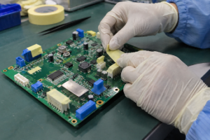
Can EBest Circuit assemble boards with customer-supplied parts?
Yes. EBest Circuit can support customer-supplied parts, turnkey sourcing, or partial turnkey assembly depending on the BOM, component condition, and production requirements.

Can EBest Circuit help if one part goes out of stock?
Yes. If a part is short or becomes long lead, EBest Circuit can review possible alternatives and bring the option back to the buyer for approval before use.

Can EBest Circuit track supplied components during production?
Yes. Supplied components can be recorded through receiving, storage, issuing, production, inspection, and shipment. This helps buyers keep clearer visibility of customer-owned parts and reduce wrong-part risk.

What files should I send for a PCB kitting review?
Send Gerber files, BOM, CPL / pick-and-place file, assembly drawings, special notes, and information about supplied components, approved substitutes, or critical parts.

What if my PCB kit is missing some parts?
EBest Circuit can review the missing items and discuss whether the buyer will ship the parts, approve substitutes, or use partial turnkey sourcing.

Can loose parts be used for SMT assembly?
Loose parts may be usable, but they need to be reviewed first. Package format, quantity, polarity, and machine handling requirements affect whether they are suitable.

Does PCB kitting reduce lead time?
It can reduce avoidable delay if the kit is complete and clearly checked before SMT. If parts are missing or unclear, kitting helps expose the issue early.

If your team has a BOM, approved MPNs, customer-supplied components, or a partial kit ready, send your Gerber files, BOM, CPL, quantity, and component list to sales@bestpcbs.com. EBest Circuit can review whether your PCB kit is ready for SMT assembly, whether any parts are short or high-risk, and whether partial turnkey support is needed before production.

You may also like