PCB manufacturing PCB manufacturing
Home > Blog

SMT Traceability Log: What Buyers Should Request

August 13th, 2026

An smt traceability log helps you isolate affected boards without holding an entire production batch. It connects each lot or serial number to the materials, process records, inspection results, tests, rework, and shipment history behind it.

Do not settle for a supplier’s “full traceability” claim. Ask what can be retrieved for one finished board and one material lot. This guide shows what evidence to request before production.

smt traceability log
A board identifier connects the finished PCBA to its production and quality history.

What Should an SMT Traceability Log Prove?

An SMT traceability log should give you a connected production history, not scattered spreadsheets and signatures. For a returned PCBA, it should answer:

  • Which PCB, component, and solder-paste lots were used?
  • Which BOM, assembly drawing, and SMT program revisions controlled the build?
  • Which line, machine, stencil, feeder setup, and production window were involved?
  • Did SPI, AOI, X-ray, ICT, or functional testing identify an abnormal condition?
  • Was the board repaired, retested, or released under an approved disposition?
  • Which other boards and shipments share the same material or process history?

The benefit is faster investigation: one identifier leads your team to the relevant build evidence. Agree on the required depth before production; a commercial assembly may need lot-level records, while a field-critical product may need unit-level linkage.

How SMT Traceability Limits a Suspect Batch

Smaller containment scope: instead of holding every board built during a broad time window, you can focus on units that share the suspect material or process history.

Backward investigation should show:

  • The work order, product revision, and production time for a failed board
  • The PCB, component, solder paste, and other controlled material lots used
  • The SMT line, machine program, stencil, and relevant process references
  • Inspection, test, repair, and retest results linked to that board or lot

Forward investigation should show:

  • Every board, panel, or work order that consumed the suspect material
  • The affected serial-number or lot-number range
  • Current inventory, work-in-process, and shipped quantities
  • Inspection, screening, repair, and release status for the affected population

The result is less unnecessary sorting, retesting, replacement, and delivery disruption. Traceability does not prove that a board is defect-free; it gives your team better evidence for containment and root-cause analysis.

Which Electronic Component Traceability Records Matter?

Faster material investigation: connect the approved BOM to the actual reel, tray, tube, or package used. An internal part number alone cannot distinguish supplier, manufacturer, date-code, or lot variations.

Useful material records may include:

  • Customer part number and manufacturer part number
  • Manufacturer and approved sourcing channel
  • Supplier lot and manufacturer lot information when available
  • Date code and quantity received
  • Internal reel, tray, tube, or package identifier
  • Incoming acceptance status
  • Moisture-sensitivity and floor-life status when applicable
  • Storage or baking records when required
  • Feeder load, replenishment, unload, and return events
  • Approved substitution or deviation reference

Specify which labels, certificates, and incoming records must be retained; they do not prove the same facts. For customer-supplied parts, define the received quantity, lot identity, acceptance condition, shortage policy, and unused-material disposition before kitting.

smt traceability log
Scanning reel and feeder identifiers helps link the actual material lot to the SMT build.

PCB Traceability Requirements for SMT Process Records

Fewer revision mistakes: PCB traceability requirements should link the approved build files to the route actually used. Correct components cannot prevent a failure caused by the wrong revision, stencil, placement program, or reflow setup.

Core process fields can include:

  • Work order and production lot
  • PCB part number, revision, and panel identification
  • BOM, centroid, assembly drawing, and SMT program revision
  • Line, machine, and production timestamps
  • Stencil identification and revision
  • Solder paste product, batch, opening time, and expiry status
  • Printer, placement, and reflow program references
  • Feeder position and material-loading confirmation where required
  • Reflow profile or approved recipe reference
  • Process alarm, interruption, or approved deviation

Not every machine parameter belongs in the customer report. The practical benefit is being able to retrieve the controlled setup when an issue occurs. During NPI, engineering changes, and repeat orders, the record should identify the released Gerber, BOM, centroid, assembly, programming, and test revisions that apply.

PCBA Traceability for Inspection, Test, and Rework

Clear pass history: PCBA traceability should link inspection and test evidence to the same board, panel, or lot. An equipment list does not prove that your assembly passed an inspection.

Depending on the agreed manufacturing plan, linked quality records may include:

  • Solder paste inspection status and relevant findings
  • AOI result, defect code, image reference, and review status
  • X-ray result for selected hidden joints or samples
  • First-article or visual inspection approval
  • ICT, flying probe, boundary-scan, or functional test result
  • Test program, fixture, procedure, or golden-sample revision
  • Repair action, replaced component, and operator
  • Retest result and final release status
  • Nonconformance, deviation, or concession reference

The log must distinguish “not required,” “not performed,” “passed,” and “no record available.” Confirm which checks are included and which need your procedures, fixtures, firmware, limits, or expected results. Repair and retest must remain visible so a reworked unit is not mistaken for a first-pass board.

smt traceability log
Board identification links inspection findings and release status to the correct PCBA.

Component-Level Traceability vs Lot-Level Traceability

Choose enough detail to protect the project without paying for unusable data. Lot-level records cost less to manage; unit- or component-level linkage can reduce the scope of field containment.

Traceability levelTypical linkageBuyer benefitImportant limitation
Lot-levelA production lot is linked to shared material and process recordsPractical for many commercial builds and repeat ordersMay not identify the exact material used on one individual board
Panel-levelA panel ID is linked to production and inspection eventsNarrows the affected population within a work orderUnit history may be lost after depanelization unless mapping is retained
Unit-levelEach PCBA serial number is linked to its route and resultsSupports precise field-return and test-history reviewRequires stable identification and consistent data integration
Component-levelA specific material lot or reel is linked to its placement or usageSupports focused material containment and where-used analysisAvailability depends on labeling, equipment integration, and replenishment control

IPC-1782 uses a risk-based approach agreed between user and supplier; it does not mean every assembly automatically receives the same record depth. Base the decision on product risk, field-replacement cost, customer requirements, volume, service life, and likely containment cost.

How PCB Component Traceability and Supplier Quality Work Together

Verify the claim before ordering: ask for a redacted record from one completed lot. It should connect the approved source and received material to the boards that consumed it. Traceability cannot compensate for weak sourcing or incoming control.

A useful audit sample should demonstrate:

  • Approved BOM and revision
  • Purchase and receiving references
  • Material labels and incoming acceptance status
  • Work order and kitting record
  • Material-to-line or material-to-board linkage
  • SMT program and controlled process references
  • Inspection and test evidence
  • Rework and retest closure, if applicable
  • Packing and shipment linkage

Test both directions: select one material lot and ask which boards used it; then select one finished board and request its materials, route, inspections, and tests. If the supplier must manually assemble unrelated files, containment may be slower than its claim suggests. Approved alternates should also carry an approval reference and affected-build identification.

Electronics Assembly Traceability Requirements Before Quotation

Fewer quotation gaps: put electronics assembly traceability requirements in the RFQ. Late requirements can change labeling, equipment setup, inspection, testing, reporting, cost, and lead time.

Define these items before quotation:

  • Required level: lot, panel, unit, or component linkage
  • Board identification method and code content
  • Customer serial-number allocation rules
  • Mandatory material, process, inspection, and test fields
  • Required label, certificate, image, or report retention
  • Record format, delivery method, and retention period
  • Applicable customer or end-market requirements
  • Treatment of customer-supplied materials and approved alternates
  • Rework, retest, deviation, and release documentation
  • Shipment label and serial-number mapping

Send released Gerber files, BOM, centroid data, assembly drawings, approved alternates, inspection criteria, test requirements, programming files when applicable, and the traceability specification.

EBest Circuit (Best Technology) can confirm the supported record scope for PCB fabrication, sourcing, SMT assembly, inspection, and agreed testing. The customer defines the required depth, regulatory obligations, acceptance criteria, firmware and functional requirements, and final product validation.

A Realistic SMT Production Traceability Example

An industrial controller PCBA returns from the field with an intermittent power fault. Its serial number leads to the work order, revisions, SMT line, power IC lot, solder paste batch, AOI result, functional test, and repair history.

A forward search then identifies every board that used the same power IC lot. If only a limited group shares that history, the customer can focus containment and additional testing on those boards. If failures cross material lots but share a production window or test setup, the investigation can move toward process or test evidence.

The customer benefit is a defensible affected population without reconstructing the build from emails, memory, and unrelated reports. Traceability supports the investigation; it does not automatically prove root cause.

Avoid a record gap after production: send the released fabrication and assembly files, BOM, volume, product requirements, and requested record package to <strong>sales@bestpcbs.com</strong>. EBest Circuit will confirm the supported linkage before the build begins.

SMT Traceability Log FAQs

What is the main purpose of an SMT traceability log? It connects a board or production lot to its materials, approved revisions, SMT process history, inspection, testing, rework, and shipment records. This helps investigate failures and isolate the affected population.

Does every PCBA need unit-level traceability? No. The appropriate depth depends on product risk, customer requirements, field-replacement cost, production volume, and the likely containment need. Many projects can use lot-level records, while others require serialized unit history.

Is MES the same as SMT traceability? No. MES can collect and connect manufacturing data, but the required identifiers, fields, equipment links, retrieval rules, and data quality still need to be defined and verified.

Which files should a buyer provide before requesting traceability? Provide the released Gerber files, BOM, centroid data, assembly drawings, approved alternates, inspection and test requirements, programming inputs when applicable, and the required traceability specification or record list.

Can a traceability log prove regulatory compliance? Not by itself. It can provide manufacturing and material evidence within an agreed scope, but the customer must define the applicable regulations, acceptance criteria, required retention period, and final compliance documentation.

You may also like

Solder Mask Defects: Causes, Checks, and Prevention

August 13th, 2026

Stop solder mask defects before they become assembly rework. A blocked pad can weaken a joint, a broken mask dam can contribute to bridging, and exposed copper can create a reliability risk.

The fastest path to a decision is to identify what the defect affects, compare it with the released requirement, and request evidence that supports acceptance, repair, or rejection.

solder mask defects
Inspect solder mask conditions before they become assembly rework.

What Are Solder Mask Defects?

Solder mask defects are unintended problems with PCB mask coverage, openings, alignment, adhesion, curing, or cleanliness. Common signs include exposed copper, mask on pads, pinholes, bubbles, peeling, cracks, contamination, and broken mask dams.

Do not approve a board from appearance alone. Confirm:

  • The affected feature and board location
  • The released Gerber and drawing revision
  • The number of affected boards
  • The applicable acceptance requirement
  • Whether the defect appeared before or after assembly

This gives you a faster, evidence-based disposition instead of a subjective appearance debate.

Common PCB Solder Mask Defects

Match the visible problem with the loss you need to prevent:

What you find What you can prevent
Mask on pads or shifted openings Weak joints and assembly delays
Exposed copper or pinholes Corrosion and reliability escapes
Blisters, peeling, or cracks Heat-triggered failures during PCBA
Broken mask dams Bridging between fine-pitch pads
Via-tenting defects Solder wicking and uneven surfaces
Debris or contamination Adhesion and cleanliness disputes

Location matters more than appearance alone. A small mark on unused laminate is not equal to the same defect on a BGA pad, test point, fine-pitch footprint, or closely spaced conductor.

Ask for a marked defect map and quantity count. You can then see whether the issue is isolated, feature-specific, panel-related, or present across the lot.

solder mask defects
Magnified inspection helps locate mask damage before component placement.

How Solder Mask Problems Affect Assembly and Reliability

Catch solder mask problems before component placement to avoid sorting populated boards later.

Mask on pads can reduce solderable area. Missing dams can increase bridging risk. Weak or undercured mask may blister, crack, or peel during baking, reflow, wave soldering, cleaning, or repair.

Exposed conductors may also lose protection against moisture and contamination. The actual field risk depends on location, spacing, voltage, cleanliness, and the product environment, so appearance alone cannot predict service life.

Early containment helps you avoid:

  • Line stoppage and emergency sorting
  • Weak joints or solder bridges
  • Damage from late-stage rework
  • Shipment delays and repeated lot disputes

Causes of Solder Mask Failure in Design and Fabrication

Separate design, fabrication, and assembly causes before asking for corrective action.

Design data: Incorrect openings, insufficient expansion, unclear via treatment, or mask dams below manufacturing capability can create repeatable defects. Confirm the minimum solder mask sliver the fabricator can hold before releasing fine-pitch data.

Fabrication: Contamination, weak surface preparation, registration error, incorrect processing, or incomplete curing can reduce coverage or adhesion.

Assembly: Excessive heat, incompatible chemistry, fixtures, handling, or repeated rework can damage an otherwise acceptable coating.

Use four checks to reach a decision faster:

Check Decision it supports
Released files and drawing Design issue or fabrication issue?
Defect map and quantity Sort, release, or remake?
Before/after assembly records When did the damage occur?
Material, cure, and process records What must change next lot?

A corrective action should change a file, note, process control, or inspection point. “Pay more attention” does not prevent recurrence.

Simple Tests for Solder Mask Damage

Use agreed tests to obtain release evidence without damaging acceptable boards.

Start with visual inspection under suitable lighting and magnification. Compare the affected area with the same feature on an unaffected board. Record exposed copper, lifted edges, cracked dams, contamination, or color transfer.

Adhesion, hardness, solvent-resistance, or controlled thermal checks may help separate weak adhesion from incomplete curing. When a customer specification calls for IPC-TM-650 testing methods for solder mask, record the exact method number and acceptance limit.

For each test, record:

  • Board revision, lot, sample size, and location
  • Before-and-after photographs
  • Method, conditions, and acceptance limit
  • Results from affected and control samples

Electrical test is not a substitute for mask inspection. A board may pass continuity while still creating soldering or protection risks.

What Inspection Evidence Should a Buyer Request?

Replace “the boards are usable” with evidence that supports your decision.

Request:

  • Close-up photographs with scale and marked locations
  • Lot, panel position, inspected quantity, and defect count
  • Confirmation of the released file and drawing revision
  • The applicable acceptance requirement
  • Test method and actual result
  • Containment status and proposed disposition
  • Root cause and corrective action for repeat defects

For repairs, also approve the material, area, cure method, final thickness, and post-repair inspection. A repair is useful only when it restores protection without reducing pad area or creating a new assembly problem.

solder mask defects
Compare the physical board, released data, and inspection record before disposition.

A Project Example: Reject, Repair, or Release?

Fine-pitch pads show mask encroachment one day before assembly. Releasing the lot risks poor wetting; rejecting every board may create unnecessary delay.

The buyer quarantines the lot and requests a defect map, measurements, file-revision confirmation, and panel-position data. The results show correct Gerber data but a repeatable registration shift in one panel position.

The evidence supports a controlled decision:

  • Release verified unaffected boards
  • Reject or remake boards outside the limit
  • Repair only with customer approval
  • Add a targeted registration check for the next lot

This illustrative example shows the customer benefit: contain first, identify the affected population, and avoid both unsafe release and unnecessary total-lot rejection.

How to Prevent Solder Mask Issues From Repeating

Confirm mask requirements before production so defects do not reach assembly.

Provide synchronized copper, solder mask, drill, and drawing data. State the mask color, finish, via treatment, acceptance standard, and any special thickness or appearance limits.

For dense BGA, fine-pitch, via-in-pad, test-point, and edge-contact areas, request a focused DFM review before releasing the order.

With EBest Circuit (Best Technology), you can confirm solder mask openings, dams, via treatment, and other manufacturability risks before they become assembly rework. You can also coordinate PCB fabrication, PCBA, and agreed inspection evidence with one manufacturing team.

Send previous defect photographs and corrective-action requirements with your RFQ. This directs the review toward the loss you want to prevent. The customer remains responsible for approved design requirements, product-level reliability targets, regulations, and final acceptance.

FAQs About Solder Mask Defects

Can a PCB with solder mask defects still be used? Possibly. Release it only after checking the affected location, quantity, drawing requirement, and assembly risk.

What causes solder mask to peel? Common causes include contamination, poor surface preparation, incomplete curing, heat, incompatible chemistry, or mechanical damage.

Can solder mask over a pad be repaired? Only when the customer approves the method and the repair restores the required solderable area without creating new damage.

Which files help prevent solder mask defects? Provide synchronized Gerbers, drill files, a fabrication drawing, revision notes, via instructions, and acceptance requirements.

What should I send for a solder mask review? Send the approved PCB files, fabrication notes, defect photographs, lot information, and inspection requirements to sales@bestpcbs.com.

You may also like

Custom Scanner PCB Board Manufacturer: Design, Prototype, and Assembly Services

August 13th, 2026

A custom scanner pcb board must do more than connect a scan engine to a host. It has to deliver stable power during illumination and data capture, protect exposed interfaces, fit the optical and mechanical assembly, support the required firmware, and remain testable after the enclosure is closed. A mistake at any one of these boundaries can produce intermittent scanning even when the bare PCB and solder joints are acceptable.

EBest supports scanner PCB design, prototyping, component sourcing, PCB assembly, and production. The project starts with the actual scan module and product requirements rather than a generic scanner schematic. This allows the quotation and engineering scope to define what EBest will manufacture, assemble, program, inspect, and test.

Custom scanner PCB board beside an imaging engine and barcode test card

What Is a Scanner PCB Board?

A scanner PCB board is the control and interconnection board that turns a scanning module into a usable product. Depending on the device, it can distribute power, receive trigger inputs, control indicators, connect the scan engine or sensor, process captured data, and send results to a computer, terminal, or industrial controller.

Processing responsibilities vary by scanner. A decoded barcode engine can return decoded characters to the host, whereas an undecoded imaging engine sends data for processing elsewhere. A flatbed scanner may also require illumination and motion control, while a fingerprint product may place matching or security functions in a separate processor or module. The module documentation therefore determines the circuit, connector, data path, and firmware responsibilities.

Which Scanner Devices Need a Custom PCB Board?

A custom board is useful when an off-the-shelf scanner module cannot directly satisfy the product’s enclosure, host interface, controls, power source, or test requirements. The board may be a compact carrier for a decoded engine or a larger controller that coordinates several scanner subsystems.

Scanner Product What the PCB Commonly Integrates Decision That Drives the Design
Handheld barcode or QR scanner Scan engine, trigger, beeper, LEDs, USB or serial connection, and power Decoded versus undecoded engine and wired versus battery operation
Fixed-mount industrial scanner Imager, machine I/O, status outputs, protected power input, and host communication Electrical environment, connector retention, grounding, and service access
Fingerprint scanner Sensor module, processor or secure module, user indication, and host interface Where image processing, matching, and security functions reside
Flatbed or document scanner Image sensor, illumination, motor control, position sensing, and data transfer Moving cable path, calibration method, motion scope, and image bandwidth
Embedded kiosk or terminal scanner Scan module, wake or trigger input, host connector, and product power Available space, optical window, mounting datum, and host protocol

A scanner control board and a camera PCB module serve different roles. A camera module centers on image capture and its local electronics. A scanner control PCB can manage the complete product interface, including power conversion, triggering, user feedback, host communication, and the connection to a separate imager.

What Information Is Required Before Starting a Scanner PCB Design?

The most important design input is the exact scan engine or sensor part number with its current integration documentation. Without that information, connector selection, voltage domains, timing, data routing, and mechanical placement cannot be verified.

  • Scanning subsystem: exact module part number, hardware guide, mating connector, cable, optical keep-out, mounting drawing, and approved alternatives.
  • Host connection: USB, UART, SPI, I2C, MIPI, parallel data, or another interface; also define logic levels, host role, protocol owner, connector, and cable length.
  • Power source: input range, battery or external supply, operating modes, available peak-current data, sequencing, sleep behavior, and charging responsibility.
  • Mechanical package: board outline, mounting holes, enclosure model, component-height limits, optical window, connector openings, FPC path, and assembly access.
  • User controls: trigger, buttons, beeper, indicators, display, vibration motor, and required default states.
  • Firmware scope: processor selection, decoding location, configuration method, programming file, version identification, and responsibility for software debugging.
  • Operating conditions: temperature, contamination, drop or vibration exposure, ESD contact points, ingress expectations, and product-level compliance requirements.
  • Acceptance criteria: required code types, reading media, operating distance, orientation, host behavior, test conditions, and pass/fail limits.

Before schematic release, organize these inputs in an interface-control table. For each connection, record the source, destination, voltage domain, direction, connector pin, default state, protection requirement, and verification method. Keep unresolved items open for engineering review instead of turning them into undocumented assumptions in the PCB files.

Scanner PCB design inputs with scan engine, FPC, USB cable, and interface planning sheet

How Should a Barcode Scanner PCB Integrate the Scan Engine, Power, and Host Interface?

Start with the scan engine’s electrical and mechanical specification, then design the power tree, data interface, connector, and control signals around that exact device. Two engines that read the same symbols can require different pinouts, voltage levels, communication paths, and host processing.

Zebra’s SE4100 and SE4107 documentation, for example, distinguishes an undecoded engine from a decoded version and lists different interface arrangements. This comparison shows why the term “barcode scanner module” is not a sufficient schematic specification. Other engines may use different interfaces.

  • Power path: size regulators and distribution from documented operating modes and transient demand. Verify rail behavior during illumination, capture, decoding, and communication, not only at idle.
  • Logic levels: check direction, high and low thresholds, idle state, pull requirements, reset conditions, and tolerance for every signal crossing a voltage domain.
  • FPC or board connector: review the mating view, pin-one reference, contact side, latch direction, stiffener, insertion depth, retention, and technician access.
  • High-speed data: apply the impedance, length, return-path, spacing, and protection requirements appropriate to the selected USB, MIPI, clock, or image interface.
  • Control sequence: document power enable, reset, trigger, wake, illumination, and status timing so the hardware design and firmware use the same states.
  • External exposure: add suitable ESD or transient protection at exposed connectors while checking its capacitance, leakage, and placement against the real interface.

Review the PCB layout and enclosure together. A correct connector footprint can still fail in the assembled product if the latch is inaccessible, the FPC is forced into an unsuitable bend, a cable crosses the optical path, or the scan engine sits outside its specified mounting position.

What Design Risks Must Be Controlled on a Scanner PCB Board?

The most damaging failures usually appear at subsystem boundaries, where each individual part can look correct but the assembled scanner is unstable. Connect every major risk to a preventive design check and a prototype measurement.

Boundary Risk Possible Product Symptom Evidence Needed Before Release
Scan engine pinout or connector orientation error No communication, wrong power connection, or damaged module Independent pin mapping, mating-view drawing, and continuity check before module installation
Power rail droop during illumination or transmission Random reset, failed reads, unstable light output, or corrupted data Oscilloscope capture at the load during defined operating modes
Incorrect logic level or startup state Intermittent communication, failure to wake, or electrical overstress Powered measurements compared with the signed interface table
Noisy return path or protection layout Data errors or sensitivity to cable, touch, or operating mode Layout review by current path followed by interface and ESD-oriented testing
FPC strain or inaccessible latch Assembly damage or intermittent contact after movement Enclosure build, bend-path inspection, retention check, and movement test
Hardware, firmware, and test revisions do not match A production unit behaves differently from the approved prototype One release baseline linking PCB, BOM, firmware, configuration, and test revision

Optical performance also has a clear responsibility boundary. Follow the scan-engine supplier’s mechanical and optical integration guidance. PCB fabrication cannot correct an obstructed field of view, unsuitable illumination geometry, a contaminated window, or a module installed outside its permitted position.

How Does Scanner PCB Prototyping Reduce Product Development Risk?

A prototype answers questions that drawings and simulations cannot close: Does the module start reliably? Does the interface recover from faults? Does the complete scanner work inside its enclosure? Assign each sample a revision and a defined test purpose.

  1. Inspect before connecting the scan engine. Verify fitted parts, polarity, connector orientation, rail resistance, and isolation to reduce the risk of damaging a high-value module.
  2. Bring up the power system in stages. Confirm every rail, reset state, enable state, current behavior, and unexpected heating before full operation.
  3. Establish host communication. Test enumeration or serial exchange, configuration, malformed or interrupted transactions, disconnects, and recovery.
  4. Measure real operating modes. Capture power and control behavior during aim, illumination, image capture, decoding, data transfer, sleep, wake, and repeated triggering as applicable.
  5. Build the mechanical assembly. Install the production-intent PCB, engine, window, cables, and enclosure to expose alignment, access, strain, and clearance problems.
  6. Run the intended reading task. Use approved symbols or documents at defined distances, angles, orientations, and operating conditions instead of relying on one clean test label.
  7. Close every issue against a revision. Record the symptom, root cause, correction, affected files, and retest result before authorizing the next build.

What Is Included in Custom Scanner PCB Assembly?

Scanner PCB assembly begins with a controlled BOM and assembly package, followed by the handling, programming, inspection, and test operations agreed for the order. The quotation distinguishes customer-supplied scan engines from manufacturer-sourced components because their procurement risk, value, and handling requirements can differ.

  • BOM validation: manufacturer part numbers, package data, quantities, designators, lifecycle status, approved manufacturers, and substitution rules.
  • Component sourcing: procurement against approved part identities, with proposed alternates held for documented approval rather than silently fitted.
  • SMT and THT assembly: placement and soldering planned around fine-pitch parts, mixed technologies, panel handling, inspection access, and rework risk.
  • Connector protection: defined storage, placement, soldering, cleaning, insertion, and packing controls for ZIF, FPC, USB, and board-to-board connectors.
  • Programming: released image, version, configuration, connector, programming method, serialization, security handling, and pass record when included.
  • Functional-test preparation: fixture, software, known-good cables, scan engine, host, test media, sequence, and objective limits supplied before production test begins.

For a customer-supplied scan engine, the work instruction also covers incoming inspection, storage conditions, traceability, connector insertion, contamination control, and responsibility for units that fail before or after integration.

How Should a Scanner PCB Board Be Inspected and Functionally Tested?

Inspection should progress from board integrity to assembly quality, powered interfaces, and finally scanner behavior. Each layer finds different defects, so a bare-board electrical pass cannot substitute for a scan test, and a successful scan cannot prove that every solder joint or protection path is acceptable.

Verification Level What It Can Confirm What It Cannot Confirm Alone
Bare PCB electrical inspection Required continuity and isolation within the agreed fabrication scope Component placement, firmware, module communication, or scan performance
Assembly inspection Presence, orientation, solder condition, connector condition, and visible contamination Correct power sequencing or complete interface behavior
Controlled power-up Rail voltage, current behavior, reset state, sequencing, and abnormal heating Reliable communication across all modes
Interface and control test Host communication, trigger, indicators, beeper, wake, configuration, and recovery Reading performance in the final mechanical assembly
Product-level scan test Defined reading behavior with the approved module, firmware, media, cable, host, and enclosure Performance outside the documented test conditions
Scanner PCB board functional testing with fixture probes, scan engine, and barcode card

Functional testing cannot be priced accurately from Gerber files alone. The manufacturer needs the expected behavior, sequence, required fixtures or fixture concept, released software, scan media, host configuration, limits, and required test record. If these inputs are not available, the quotation should list test development and missing customer inputs as open items.

How Do You Move a Scanner PCB Board from Prototype to Volume Production?

Production release is a configuration-control decision, not simply a larger prototype order. The approved board, BOM, scan engine, firmware, enclosure, programming method, and functional test must all point to the same baseline.

  1. Close prototype issues: assign every issue a disposition and verify each correction on the affected revision.
  2. Release matching manufacturing files: fabrication data, drawings, stackup, BOM, placement data, assembly instructions, and approved deviations must carry compatible revisions.
  3. Freeze component decisions: identify approved parts, controlled alternates, customer-supplied materials, and the approval path for future substitutions.
  4. Bind firmware to hardware: release the production image, configuration, programming procedure, version check, and security requirements.
  5. Approve the test baseline: define fixtures, software, media, known-good references where applicable, limits, failure handling, and retained records.
  6. Review the first production build: compare the output with the validated sample before increasing quantity.
  7. Control later changes: assess PCB, BOM, firmware, scan-engine, process, and test changes for revalidation impact.

This release package gives engineering, purchasing, quality, and manufacturing the same definition of an acceptable unit. It also prevents a component substitution or firmware update from silently breaking a scanner function that worked during prototyping.

What Scanner PCB Manufacturing Services Does EBest Provide?

EBest provides PCB design, PCB prototyping, component sourcing, PCB assembly, and mass production services. For a scanner project, these services can be quoted separately or combined after the input files, responsibilities, and acceptance criteria are reviewed.

Service Customer Input Scope to Confirm in the Quote
Scanner PCB design Product requirements, module guide, interfaces, mechanics, firmware boundary, and test criteria Schematic, layout, reviews, design files, and validation responsibilities
PCB prototype Released fabrication data, quantity, stackup, materials, and inspection requirements Bare-board build, documentation, schedule, and acceptance
Component sourcing Controlled BOM, approved manufacturers, alternate policy, and consigned-parts list Procurement responsibility, approval records, and traceability
PCB assembly BOM, placement data, assembly drawings, special instructions, and panel information SMT/THT operations, inspection, programming, cleaning, handling, and packing
Mass production Validated release baseline, order quantity, forecast, change controls, and test package Production revision, records, test coverage, packaging, and delivery terms

How Does EBest Support Scanner PCB Design and Engineering Review?

Engineering support turns product requirements into reviewable interfaces and manufacturable release files. Work can begin with a requirement set, an existing schematic and layout, or a complete manufacturing package. The deliverables depend on the maturity of the customer’s design.

For a new design, the review can cover the scan-engine connection, power architecture, host interface, controls, protection, board outline, component placement, FPC access, programming, and planned test points. For customer-supplied PCB files, the review can focus on fabrication clarity, footprint-to-BOM consistency, assembly access, polarity, panel requirements, component availability, and whether the stated programming and test scope is executable.

Responsibilities also need to be explicit. The scan-engine supplier may own optical performance and module firmware; the product developer may own the enclosure and application software; the PCB team may own power, connectivity, layout, and manufacturing data. Defining those boundaries before the prototype prevents a failure from being passed between suppliers without a measurable owner or acceptance criterion.

How Does EBest Manage Components for Scanner PCB Assembly?

Component control protects the validated electrical function, footprint, firmware compatibility, and mechanical fit of the scanner PCBA. Availability or price alone is not enough to approve an alternate.

The production BOM identifies the manufacturer part number, package, quantity, reference designators, approved manufacturer list, customer-supplied parts, and substitution status. Give priority to the scan engine, processor, memory, power devices, clock components, FPC/ZIF connectors, USB connectors, protection parts, beeper, and indicators. A visually similar part may have a different pinout, interface behavior, tolerance, lifecycle, or firmware requirement.

Before releasing a substitute, compare its electrical ratings, pin and package compatibility, mechanical clearance, firmware impact, regulatory relevance where applicable, and required validation tests. Record the approval against the production revision so procurement changes remain visible to engineering and quality.

What Files Are Needed for a Scanner PCB Manufacturing Quote?

An accurate quote separates PCB fabrication, assembly, programming, testing, and commercial requirements. Listing missing inputs as open items prevents them from being hidden inside a provisional price.

  • PCB fabrication: Gerber or ODB++, drill files, fabrication drawing, board outline, stackup, material, copper, surface finish, impedance, marking, panel, and applicable acceptance requirements.
  • Assembly: revision-controlled BOM, pick-and-place data, assembly drawings, polarity information, special process notes, customer-supplied parts, and substitution rules.
  • Mechanical integration: enclosure model or drawing, scan-engine mounting data, connector openings, keep-outs, height limits, optical window, FPC route, and cable drawings.
  • Programming: released image, configuration values, method, connector or fixture definition, security handling, serialization, and version-verification rule.
  • Functional test: test sequence, instruments or fixture concept, software, approved scan engine, cables, host, scan media, objective limits, and required report fields.
  • Commercial requirements: prototype and production quantities, delivery destination, requested schedule, packaging, forecast, and change-control contacts.

Why Choose EBest as Your Scanner PCB Manufacturer?

Choose EBest when you want one manufacturing partner to carry your scanner PCB from design review and prototyping through sourcing, assembly, and production. Keeping these stages connected helps reduce handoff gaps between separate design, PCB, purchasing, and assembly suppliers.

  • Find integration problems before they reach a larger build. The review can check scan-engine pinout, power, connector orientation, board outline, FPC access, programming, and test requirements before prototype release.
  • Keep the validated design consistent during production. PCB files, BOM, approved component alternatives, firmware inputs, and test requirements can be controlled against the same project revision.
  • Reduce sourcing uncertainty. Component sourcing and PCB assembly can be coordinated from the approved BOM, while proposed substitutions remain subject to customer or engineering approval.
  • Receive a clearer quotation. The review identifies included services, customer-supplied parts, missing inputs, programming responsibilities, and functional-test scope before the order is placed.
  • Support both development and production needs. EBest provides PCB design, PCB prototyping, component sourcing, PCB assembly, and mass production services.

EBest Circuit was established on June 28, 2006. Its certifications and compliance credentials include IATF 16949, ISO 9001:2015, ISO 13485:2016, AS9100D, REACH, RoHS, and UL. Current documents and the applicable scope can be provided for supplier qualification.

Send your scan-engine documentation, Gerber/ODB++, BOM, quantity, enclosure constraints, programming method, and test requirements. EBest can review the package and prepare a quotation based on the services and deliverables your scanner project actually needs.

FAQs About Scanner PCB Boards

Q1: Is a QR code scanner PCB different from a barcode scanner PCB?

Not necessarily. “Barcode scanner” can include 1D and 2D products, while QR reading requires a 2D-capable imaging and decoding path. The engine interface and processing architecture, rather than the product label, determine whether the PCB must change.

Q2: Can one PCB support both 1D and 2D barcode scan engines?

Yes, when both engines are compatible with the board’s power, connector, interface, mechanical space, control signals, and firmware. A common connector does not prove drop-in compatibility; both integration guides must be compared.

Q3: What is the difference between decoded and undecoded scan engines?

A decoded engine returns decoded results to the host. An undecoded engine requires image or sensor data to be processed elsewhere. The choice affects processor workload, software responsibility, data interface, and connector definition.

Q4: Can a barcode scanner PCB use both USB and UART interfaces?

It can if the selected engine and system architecture support both. The design must provide the correct routing, logic levels, protection, connectors, and firmware selection behavior. Confirm both interfaces for the exact engine part number.

Q5: Does a battery-powered scanner require a different PCB design?

Usually. Battery operation adds energy budgeting, transient-load response, low-voltage behavior, sleep and wake control, and potentially charging, protection, and fuel-gauge functions. The battery profile and scan-engine operating modes must be reviewed together.

Q6: How is a fingerprint scanner PCB different from a barcode scanner PCB?

The sensor, processing, security boundary, interface, mechanics, firmware, and validation method can all differ. A fingerprint module should be integrated as its own controlled subsystem, not treated as a barcode-engine substitute.

Q7: What should be considered when designing a flatbed scanner PCB?

Define the image-sensor interface, illumination, motion-control responsibility, home or limit sensing, moving-cable path, calibration, data bandwidth, and enclosure geometry. Cable life and calibration ownership should be included in the validation plan.

Q8: Can the scan engine be replaced without redesigning the entire PCB?

Only if the replacement remains compatible with the existing power, pinout, logic levels, protocol, firmware, mechanics, thermal conditions, and optical arrangement. Any failed comparison may require a PCB or product change.

Q9: How is a scanner control PCB different from a camera PCB module?

A camera module concentrates on image capture. A scanner control PCB can manage the broader product functions, such as power, trigger, indicators, host communication, peripheral control, and a separate scan engine. The two boards can coexist in the same product.

Q10: Can EBest support scanner PCB prototypes and volume production?

Yes. EBest provides PCB prototyping, PCB assembly, component sourcing, and mass production services. The quotation defines the deliverables after review of the design, BOM, quantities, assembly, programming, and test package.

Conclusion

A production-ready scanner pcb board begins with one defined scan engine, a controlled interface table, a realistic enclosure model, and measurable acceptance criteria. Prototype work should close power, communication, connector, firmware, mechanical, and scanning risks before the manufacturing files are frozen.

For scanner PCB design, prototyping, component sourcing, assembly, or production support, send your Gerber/ODB++, BOM, quantity, stackup, scan-engine documentation, enclosure constraints, assembly details, programming method, and test requirements to sales@bestpcbs.com for engineering review and a quotation.

You may also like

PCB Interposer: Stackup, Routing, DFM, and Testing

August 13th, 2026

A PCB interposer is an intermediate printed circuit board that remaps pads, pins, power rails, or signals between two incompatible interfaces. Typical uses include adapting a new BGA to a legacy footprint, expanding a fine-pitch device into a testable array, and connecting boards or sockets with different pin assignments. Its design must control the complete transition from the first pad field through vias and routing to the second interface.

Organic PCB interposer with dense BGA pads and routed copper connections

Do You Need an Organic PCB Interposer or a Package-Level Interposer?

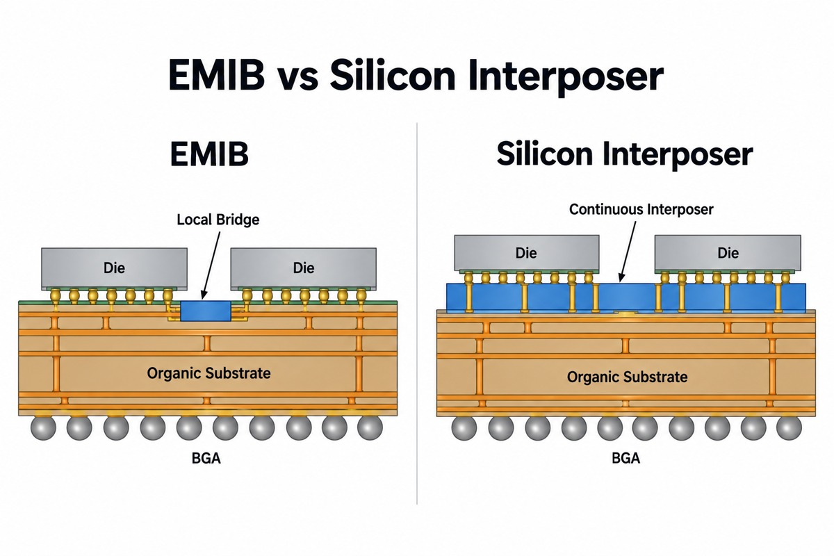
Choose the supplier from the interconnect level, not from the word interposer. An organic PCB interposer is fabricated with laminate, copper circuitry, plated holes or microvias, solder mask, and a board-level surface finish. A silicon interposer uses semiconductor processes and may contain through-silicon vias. Glass and advanced package substrates also require different fabrication equipment and qualification methods.

Structure Connection Level Typical Fabrication Route Primary Design Constraint
Organic PCB interposer Package-to-board, board-to-board, socket, or test interface Multilayer PCB or HDI processes BGA escape, via geometry, planarity, impedance, and assembly
IC package substrate Die or package to system board Fine-line organic substrate processes Package warpage, fine pitch, and substrate reliability
Silicon interposer Die-to-die or die-to-package in 2.5D integration Semiconductor lithography, often with TSVs Microbump density, TSV design, and thermal stress
Glass interposer Advanced package redistribution Specialized glass-via and metallization processes Via formation, metallization adhesion, and handling

If the input data contains bare-die bumps, microbumps, TSVs, redistribution layers, or package-level warpage requirements, route the project to an advanced-packaging supplier. If both sides are conventional pads, BGA lands, connectors, sockets, or test contacts that can be built with PCB processes, continue with an organic PCB feasibility review.

Which Inputs Must Be Fixed Before Stackup Design?

Freeze both mating interfaces and their electrical mapping before selecting layer count or via type. The design team needs controlled coordinates, orientation, pin names, mechanical datums, installed height, attachment method, and service conditions for both sides. A mirrored footprint or outdated pin map can produce a board that passes fabrication inspection but connects the wrong nets.

  • Interface geometry: provide pad coordinates, package drawings, body outline, keepouts, datum locations, connector or socket drawings, and allowable positional error.
  • Pin mapping: identify every signal, ground, power, no-connect, reserved pin, polarity mark, and remapped connection in a controlled table.
  • Electrical limits: state impedance, current, voltage spacing, differential-pair skew, insertion-loss budget, and any sensitive analog or clock nets.
  • Assembly route: define soldered, socketed, compression-contact, or test-only use; also state which side is assembled first and the number of thermal cycles.
  • Mechanical limits: specify total thickness, flatness or coplanarity, component clearance, support points, contact force, and allowable board deflection.
  • Service profile: include operating and storage temperature, vibration, expected mating cycles, moisture exposure, cleanliness, and target life.

How Should the BGA Escape and Stackup Be Built?

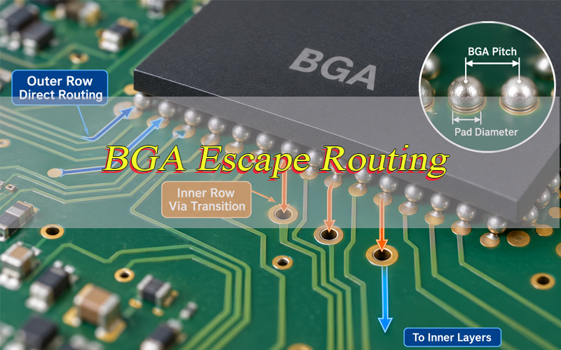
Derive the stackup from routing channels, reference-plane continuity, and manufacturable via transitions. Start by grouping pins into ground, power, high-speed, low-speed, analog, clock, and unused classes. Then estimate how many traces must leave each BGA ring and which layer changes are unavoidable.

Engineer reviewing PCB interposer stackup and dense BGA escape routing
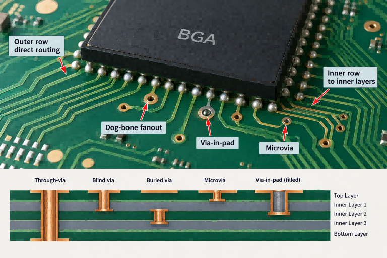
  1. Route the outer rows: use surface escape where trace width, clearance, and solder-mask geometry provide adequate manufacturing margin.
  2. Assign via structures: use through holes when pitch permits; introduce blind microvias or via-in-pad only where inner rows cannot escape otherwise.
  3. Reserve reference planes: keep controlled-impedance signals adjacent to continuous ground and provide nearby ground transitions at every signal-layer change.
  4. Distribute power: size copper and via arrays from current and transient requirements, then place decoupling where the connection inductance remains useful.
  5. Check lamination sequence: map each blind and buried via to a real build stage; stacked microvias and multiple sequential laminations require an explicit reliability review.
  6. Balance copper: correct large density differences between the central pad field and the perimeter to reduce bow, twist, and registration variation.

Via-in-pad must be called out as filled, capped, and planarized when the pad will be soldered. Leaving the construction undefined can cause solder loss into the via, insufficient joint volume, and uneven pad surfaces. Backdrilling may reduce through-via stubs, but it requires adequate stub access, drill tolerance, and clearance from adjacent structures.

Which Parameters Control Signal and Power Integrity?

Analyze the pad, via, trace, plane reference, and mating joint as one electrical discontinuity. Short interposers can still degrade fast interfaces because their transitions may contain large pads, long via stubs, anti-pad changes, or interrupted return paths.

  • Impedance: calculate from the proposed production stackup, including finished copper, dielectric thickness, resin content, trace geometry, and fabrication tolerance.
  • Return path: prevent plane splits and voids below fast routes; place ground vias close to signal vias when the route changes layers.
  • Via discontinuity: evaluate barrel length, unused stub, pad diameter, anti-pad diameter, and nearby ground-via placement.
  • Differential symmetry: match the two paths through pads and vias, not only along straight traces; control intra-pair skew at the transition.
  • Crosstalk: evaluate spacing together with parallel length, edge rate, reference distance, and allowable coupled noise; a fixed spacing ratio is not a universal acceptance rule.
  • Power impedance: minimize loop inductance through paired power-ground vias, suitable plane spacing, and decoupling connected with short, wide paths.

Use impedance coupons for fabrication control, TDR for time-domain discontinuity location, and S-parameters or an end-to-end link test when insertion loss, return loss, or crosstalk is part of the interface budget. Match the test method and frequency range to the actual signal instead of using a generic high-speed label.

What Manufacturing Limits Require an Early DFM Review?

No single minimum-feature value proves that a dense interposer is manufacturable. Pad pitch must accommodate trace escape, capture pads, anti-pads, solder-mask openings, registration allowance, copper thickness, via fill, and the selected lamination sequence at the same time.

Capability Item General Capability Special Process or Review
FR-4 layer count 1-10 layers; high-Tg material noted for 8 layers and above 10-32 layers
Laser blind or buried via diameter 0.10 mm Project-specific stackup review
Minimum finished mechanical hole 0.20 mm 0.15 mm
Through-hole aspect ratio 8:1 10:1
Inner-layer line/space at 0.5 or 1 oz 4/4 mil 3/3 mil
Outer-layer line/space at 1 oz 4/4 mil 3/3 mil
Solder-mask opening, single side 2 mil 1 mil
ENIG thickness Gold 0.025-0.125 micrometers; nickel 3-8 micrometers Confirm against pad function and assembly criteria

These values come from the current general PCB capability workbook and are feasibility boundaries, not automatic design rules. EBest Circuit must review the actual BGA map, copper weight, material, panel construction, via sequence, solder-mask strategy, and acceptance criteria before confirming a special-process design.

How Is an Organic PCB Interposer Manufactured?

Organic PCB production is the base process. Dense pad fields add tighter controls for registration, via filling, planarity, and copper balance.

  1. Verify data: compare the netlist, layer stack, drill pairs, pin map, dimensions, impedance notes, and finish requirements before tooling.
  2. Form inner layers: image and etch copper, then inspect line width, spacing, annular rings, and defects before lamination.
  3. Laminate the structure: control resin flow, dielectric thickness, copper distribution, and layer registration across each build cycle.
  4. Create interconnects: drill mechanical holes or laser microvias, desmear, metallize, and plate to the specified layer pairs.
  5. Fill via-in-pad: fill, cure, planarize, and cap solderable pads so that the assembly surface remains flat and sealed.
  6. Form outer layers: image and etch the final circuitry, then inspect critical pads, traces, and clearances.
  7. Apply mask and finish: control solder-mask registration and apply the approved surface finish for soldering or contact use.
  8. Profile and test: route the outline, inspect dimensions, perform electrical test, and complete the defined coupon or microsection checks.

Which Failure Modes Should the Design and Test Plan Control?

Each critical failure needs a defined prevention method and a measurable detection method. Continuity testing alone cannot detect planarity, joint fatigue, impedance discontinuities, or weak microvias.

Failure Mode Primary Cause Design Control Verification
Wrong net connection Mirrored footprint, orientation error, or uncontrolled pin-map revision Independent coordinate and netlist comparison Electrical test against the approved netlist
Solder wicking Open or incompletely filled via-in-pad Filled, capped, and planarized construction Cross-section and assembly inspection
Open or intermittent joint Warpage, contamination, inadequate solder volume, or unstable contact force Flatness, finish, stencil or socket, and support controls X-ray, coplanarity measurement, and continuity under load
Signal reflection Via stub, pad/anti-pad discontinuity, or reference-plane interruption Transition modeling and controlled return path TDR, S-parameters, or link test
Microvia fatigue Stacked geometry, high thermal stress, or unsuitable lamination sequence Via-structure and stackup reliability review Thermal cycling with resistance monitoring and cross-section
Pad or laminate damage Board bending, socket force, shock, or poor support Mechanical load-path and thickness review Strain measurement, mechanical test, or destructive analysis

How Should the Finished PCB Interposer Be Validated?

Validate in four stages: data correctness, bare-board quality, assembled-interface quality, and application performance.

Technician inspecting and probing a finished PCB interposer
  • Data comparison: verify fabrication data, drill pairs, stackup, netlist, and pin-map revision before production release.
  • Dimensional inspection: measure thickness, outline, datum locations, hole and pad positions, and bow or twist where mating alignment depends on them.
  • Electrical test: check opens and shorts; add four-wire resistance limits for low-resistance power or measurement paths when required.
  • Microsection: inspect plating, via fill, registration, dielectric condition, and interconnect structure on representative coupons or boards.
  • Assembly inspection: evaluate hidden solder joints by X-ray and inspect bridging, voiding, solder volume, wetting, and alignment against defined limits.
  • Signal verification: use impedance coupons, TDR, S-parameters, or a functional link test according to the electrical risk.
  • Reliability verification: select thermal cycling, vibration, mechanical loading, or mating-cycle testing from the actual service profile.

The purchase specification must name the test, sampling level, equipment or method, numerical acceptance limit, and disposition for failure. “100% electrical test” is meaningful only when the controlled netlist and tested characteristics are identified.

What Determines PCB Interposer Cost and Supplier Suitability?

PCB interposer cost is driven by the number of special operations and the manufacturing margin left around critical features. A small board can still be expensive when it requires sequential lamination, stacked or filled microvias, fine line/space, tight registration, controlled flatness, impedance coupons, or extensive inspection. Quantity and panel utilization matter, but they do not remove the cost of a complex build sequence.

Cost Driver Why It Changes the Quote RFQ Action
Layer and lamination structure Additional build cycles increase processing, registration control, inspection, and failure exposure. Request the proposed stackup and a layer-pair diagram for every blind or buried via.
Microvia and via-in-pad construction Laser drilling, filling, planarization, copper capping, and stacked structures add controlled operations. Identify which pads require filled and capped vias; do not apply the requirement to every via by default.
Fine features and tolerances Line/space, annular ring, solder-mask registration, positional accuracy, thickness, and flatness interact and can reduce yield margin. Mark each tolerance as functional, preferred, or open to supplier proposal.
Material and surface finish Material availability, stackup thickness, copper weight, finish type, and finish thickness affect sourcing and process compatibility. State the required electrical, thermal, soldering, or contact function instead of naming an unsupported substitute.
Electrical control Controlled impedance, low-resistance paths, and high-frequency limits require stackup calculations, coupons, or additional measurements. List the controlled nets, target values, tolerances, test method, and required report.
Inspection and reliability evidence Dimensional reports, microsections, X-ray, TDR, S-parameters, thermal cycling, and traceability add work only when specified as deliverables. Separate mandatory production acceptance from qualification or optional engineering tests.
Assembly responsibility Bare-board supply, solder-ball attachment, component assembly, socket integration, and functional testing have different tooling and quality ownership. Define the delivery state and assign responsibility for each mating interface.

Compare quotations only after normalizing their scope. One supplier may include via filling, impedance coupons, electrical test, dimensional reporting, and assembly inspection, while another may quote only the bare board. Ask each supplier to identify exclusions, special-process charges, tooling, test coverage, supplied reports, and the design changes assumed in the price.

A technically suitable supplier should return a manufacturable stackup, a complete via sequence, the features that consume the smallest process margin, and any proposed changes to pads, anti-pads, mask openings, copper balance, or tolerances. The response should also identify which operations are performed and controlled within its qualified supply chain. Silicon, glass, and bare-die package structures require an advanced-packaging route and should not be evaluated as conventional PCB work.

What Should Be Included in the Engineering Review Package?

The review package must reproduce both interfaces without assumptions. It must also control their mapping, board construction, and acceptance criteria.

  • Fabrication package: Gerber X2 or ODB++, NC drill files with layer pairs, IPC-356 or equivalent netlist, fabrication drawing, outline, and stackup.
  • Interface package: land-pattern coordinates, package and connector drawings, pin maps, orientation, datums, keepouts, and height limits.
  • Electrical package: net classes, impedance and skew limits, current by rail, voltage spacing, loss budget, and required measurements.
  • Material package: laminate performance requirements, copper weight, solder mask, surface finish, and restricted-substance requirements.
  • Assembly package: BOM where applicable, centroid data, paste intent, reflow limits, inspection criteria, and handling controls.
  • Quality package: acceptance class or customer specification, sampling, coupon plan, dimensional report, microsection criteria, traceability, and reliability tests.

Mark every requirement as mandatory, preferred, or open to supplier proposal. This prevents inherited layout habits from being treated as fixed system requirements and makes DFM changes auditable.

FAQs About PCB Interposer

Q1: Can one PCB interposer support several package variants?

A1: Only when the pad geometry and pin mapping remain unambiguous. Shared pads, jumpers, or option components must not create unterminated stubs, accidental shorts, or an assembly configuration that cannot be inspected.

Q2: When is a socketed interposer preferable to a soldered one?

A2: Use a socket when replacement, repeated testing, or device preservation is more important than minimum height and transition loss. Confirm contact resistance, force, wear, alignment, and bandwidth.

Q3: Does a thicker interposer improve reliability?

A3: Not automatically. Greater thickness can increase stiffness but also lengthen vias and change solder-joint or socket loading; evaluate electrical and mechanical effects together.

Q4: Can ENIG be used for every interposer contact?

A4: ENIG is common for solderable pads, but the contact function determines the finish. Repeated mechanical contacts, wire bonding, fine-pitch assembly, or special storage requirements may require another finish and separate confirmation.

Q5: When is backdrilling worth adding?

A5: Add backdrilling when the unused through-via stub consumes a meaningful part of the channel budget. Confirm remaining stub, drill tolerance, accessible side, and nearby-clearance limits before release.

Q6: Should unused BGA pads be removed?

A6: Remove or retain them only after checking routing space, assembly balance, inspection needs, and future variants. Unused pads must not be mistaken for connected or testable nodes.

Q7: How should orientation be controlled?

A7: Use at least two independent controls. Combine pin-one marking with asymmetric datums, keyed mechanical features, coordinate tables, or an assembly drawing that cannot be mirrored.

Q8: Is a functional test enough for production acceptance?

A8: Functional testing does not replace bare-board netlist testing or structural inspection. It may miss latent microvia, plating, dimensional, and process defects that have not yet caused system failure.

Q9: When should a test coupon be added?

A9: Add a coupon when production verification requires a representative structure that cannot be measured reliably on the finished board. Examples include impedance, plating, microvia, and lamination checks.

Q10: What must be controlled when the interposer is reworked?

A10: Limit cumulative heat, pad damage, laminate moisture, and mechanical bending. Define the permitted rework cycle, thermal profile, cleaning method, inspection, and acceptance test before reusing the assembly.

Conclusion

A reliable PCB interposer begins with controlled interface data and ends with measurable acceptance evidence. Freeze both pad fields and the pin map, derive the stackup from escape and reference requirements, review every via against the real build sequence, and connect each failure risk to a defined inspection or test.

For an organic PCB interposer review, send the fabrication data, pin maps, stackup, impedance targets, assembly method, service profile, and acceptance criteria to sales@bestpcbs.com. EBest Circuit will review the printed-board construction and identify features that require special-process confirmation.

You may also like

Best AI Server PCB Manufacturer From Design to Assembly

August 11th, 2026

An AI Server PCB project succeeds when its electrical and mechanical requirements survive every handoff from architecture and layout to fabrication, assembly, and testing. The central task is to preserve signal, power, thermal, and mechanical margin in a construction that can be manufactured repeatedly.

Before layout begins, define the board’s role, interface generations, power profile, cooling conditions, connector locations, mechanical limits, and acceptance tests. These inputs determine the materials, stackup, via structure, manufacturing controls, and quotation scope.

AI Server PCB manufacturing review on a large server-class circuit board

What Is an AI Server PCB?

An AI server PCB is a circuit board that carries one or more compute, memory, networking, storage, control, or power functions inside an AI server. Fast interfaces, concentrated power, dense packages, large board formats, and continuous workloads make these boards more demanding than their basic copper-and-dielectric construction suggests.

The term can refer to a host motherboard, accelerator baseboard, network switch board, power distribution board, backplane, or management board. Requirements depend on the processors, interfaces, power rails, connectors, and cooling conditions assigned to that board. Defining its role gives the designer and manufacturer a sound basis for the stackup, materials, via structure, and test plan.

Which PCB Boards Are Used in an AI Server?

An AI server normally uses several PCB boards to perform different system functions. The exact combination depends on the server architecture; common board types are listed below.

PCB Board Primary Function
Host motherboard Connects the CPU, memory, storage, management controller, and expansion devices
Accelerator baseboard Connects GPUs or other accelerator modules and supports communication between them
Network or switch board Transfers data between accelerators, servers, and external networks
Power distribution board Distributes or converts power for processors, accelerators, and other server loads
Backplane Connects multiple server boards, storage devices, or modules through a shared interface
Riser board Changes the orientation or position of expansion cards within the server chassis
Management board Monitors server status and supports remote control, diagnostics, and system management
Storage board Connects and controls SSDs, hard drives, or other storage devices

Not every AI server uses every board listed above. Some functions may be combined on one PCB, while modular platforms may separate them across several boards. Identifying the board type and its function prevents a host motherboard, accelerator baseboard, backplane, or power board from being quoted as though they were the same product.

How Is an AI Server PCB Different from a Standard Server PCB?

An AI server PCB differs from a standard server PCB mainly in accelerator connectivity, local power demand, routing density, cooling loads, and the validation needed to prove stable operation. The exact difference depends on the server architecture, but the board-level comparison below shows the usual design shift.

Comparison Area Standard Server PCB AI Server PCB
Board architecture Primarily connects CPUs, memory, storage, management, and network interfaces Adds dense GPU or accelerator modules and the high-bandwidth fabric that connects them
High-speed routing Channel count and routing density follow conventional server interfaces More simultaneous accelerator and fabric links increase breakout, reference-plane, via-transition, and crosstalk constraints
Power delivery Power planes and regulators support conventional processor, memory, storage, and network loads Higher localized current and faster load changes near accelerators demand lower-impedance power paths, stronger decoupling, and closer thermal review
Materials and stackup High-Tg FR-4 or other materials may be sufficient when the verified channel budget allows Long or fast accelerator links may require lower-loss laminate, tighter impedance control, shorter stubs, and additional routing or power-distribution layers
Thermal and mechanical design Board support and cooling are sized for the standard component and heat-sink arrangement Large packages, heavier cooling hardware, concentrated heat, and connector density increase the need to control board support, airflow, bow, twist, and mating alignment
Validation scope Bare-board, assembly, functional, and platform tests confirm the specified server design Validation must also correlate channel margin, power behavior, temperature, mechanical fit, and workload stability across the accelerator platform

A standard server stackup should therefore be reused only after its channel loss, reference planes, power distribution, via structure, board support, and thermal margin have been checked against the AI server architecture.

Why Does an AI Server PCB Need High-Speed and High-Power Design?

An AI server PCB needs high-speed design to move large amounts of data between processors, memory, accelerators, storage, and network interfaces, and it needs high-power design to deliver stable current to those devices under rapidly changing workloads. If either side is inadequate, the server may lose interface margin, suffer voltage instability, overheat, or throttle before it reaches its intended performance.

High-speed design protects signal integrity. Package escape, trace geometry, dielectric loss, copper roughness, vias, reference-plane transitions, connectors, and module interfaces all contribute to channel loss and reflections. The PCB therefore needs controlled impedance, continuous return paths, appropriate materials, and transition structures that keep the complete channel within its electrical budget.

High-power design protects power integrity and temperature margin. Accelerators can draw high local current and change load quickly, so power planes, copper distribution, vias, voltage regulators, and decoupling must limit voltage drop and transient noise while carrying current without excessive heating.

The two requirements must be reviewed together. Dense signal routing can reduce the space available for power copper, while plane splits, large via fields, and copper imbalance can affect return paths, lamination, and thermal behavior. The design target is sufficient signal and power margin under the intended workload and operating temperature—not maximum performance in only one domain.

How Should an AI Server PCB Be Designed?

An AI server PCB should be designed in a controlled sequence from system requirements to a verified production package. Signal, power, thermal, mechanical, manufacturing, and test decisions must be developed together because a change in one area can reduce margin in another.

  1. Define the board role: Identify whether the PCB is a host motherboard, accelerator baseboard, network board, power board, backplane, riser, management board, or storage board, then define its interfaces with the rest of the server.
  2. Set measurable constraints: Record interface generations and channel budgets, rail voltages and current profiles, board outline, connector locations, component heights, cooling zones, mounting points, and required validation results.
  3. Select materials and stackup: Choose laminates, copper weights, layer functions, reference planes, impedance structures, and via types that meet electrical and reliability needs while remaining manufacturable.
  4. Place critical components: Position processors, accelerators, memory, regulators, clocks, connectors, and decoupling parts to shorten sensitive paths, support airflow, and leave realistic breakout and assembly space.
  5. Design the power distribution network: Size planes, pours, vias, regulator connections, and decoupling for DC voltage drop, transient response, current density, and temperature rise at the expected workload.
  6. Route high-speed interfaces: Maintain controlled impedance and continuous return paths, limit discontinuities and stubs, manage lane spacing and length requirements, and review packages, vias, connectors, and cables as one channel.
  7. Review thermal, mechanical, and DFM risks: Check copper balance, heat-sink and board-support loads, airflow, warpage, connector alignment, drill and registration limits, assembly access, and test-point availability.
  8. Verify and release the design: Close signal, power, thermal, mechanical, DFM, and test findings, then issue one synchronized revision of the fabrication data, drawings, stackup, netlist, BOM, assembly files, and acceptance criteria.

Which Materials and Stackups Are Suitable for an AI Server PCB?

AI server PCBs typically use high-Tg FR-4, mid-loss laminate, or low-loss high-speed laminate, selected according to the function and channel budget of each board. Accelerator baseboards and network or switch boards usually need the lowest-loss construction. Host motherboards often combine high-speed routing with substantial power distribution. Management and lower-speed storage boards may use high-Tg FR-4 when verified channel loss remains within the interface budget.

AI Server PCB Type Suitable Material Direction Stackup Priorities
Accelerator baseboard Low-loss laminate with controlled dielectric properties and low-profile copper for long, fast processor-to-processor or processor-to-module links Critical signal layers beside continuous ground references, short via transitions, sufficient power and ground planes, and balanced copper distribution
Network or switch board Low-loss high-speed laminate selected from the total connector, via, and trace loss budget Closely referenced differential-pair layers, controlled breakout and backdrill structures, isolation between channel groups, and stable return paths through connectors
Host motherboard Mid-loss or low-loss laminate for high-speed regions, with high-Tg and reliability characteristics suitable for the complete board Separate routing, reference, and power-distribution functions; enough breakout layers for dense packages; and plane pairs positioned to support return current and decoupling
Power distribution board High-Tg laminate with copper thickness and thermal behavior matched to the required current; low-loss dielectric is usually not the primary need Wide copper areas, parallel power and ground paths, adequate via arrays, thermal balance, insulation spacing, and mechanical support for high-current connections
Backplane or riser Mid-loss or low-loss laminate when it carries high-speed fabrics; high-Tg FR-4 may suit lower-speed control or power-only connections Connector-launch control, continuous references, short transitions, mechanical thickness control, and balanced construction for mating alignment
Management or storage board High-Tg FR-4 for moderate-speed functions, upgraded to a mid-loss material when interface length and speed require more channel margin A simpler multilayer stackup with clear signal references, practical power planes, manufacturable vias, and enough test access

The layer count should not be chosen from the term “AI server” alone. It is determined by package escape, routing density, reference-plane continuity, current distribution, board thickness, via aspect ratio, and mechanical balance. Adding layers without assigning each one a necessary function increases cost and fabrication difficulty without guaranteeing better electrical performance.

Final material approval should be based on the complete channel and construction. Confirm dielectric data at the relevant frequency, copper profile, glass style, resin system, thermal expansion, CAF resistance, availability, pressed thickness, impedance geometry, and fabricator capability. If two laminate families are combined, their bonding, drilling, registration, and thermal compatibility must be reviewed before release.

What Should Be Checked During an AI Server PCB DFM Review?

An AI server PCB DFM review should check the stackup, via architecture, registration margin, copper balance, assembly geometry, and test access against both factory capability and the board’s electrical and mechanical intent. A minimum trace-and-space check alone cannot reveal whether the complete construction is manufacturable.

  • Stackup definition: Confirm material designations, pressed dielectric thicknesses, copper weights, impedance structures, finished board thickness, and permitted material alternatives. The fabrication drawing, impedance table, and layer data must describe the same construction.
  • Via architecture: Review drill sizes, finished hole sizes, aspect ratios, annular rings, capture pads, drill-to-copper clearances, laser-via cycles, buried vias, and backdrill depths as one interconnection system.
  • Registration margin: Check that fine-pitch escapes, dense via fields, plane clearances, and backdrill targets retain enough tolerance for imaging, lamination, and drilling variation.
  • Impedance and return paths: Match the proposed trace geometries to the approved stackup and confirm that reference planes remain continuous through layer changes, connector launches, and high-density breakout regions.
  • Copper and mechanical balance: Review local copper density, plane distribution, board thickness, panel orientation, heavy components, and heat-sink loads to reduce plating variation, bow, twist, and assembly distortion.
  • Assembly geometry: Verify pad and solder-mask geometry, component spacing, polarity markings, stencil-sensitive packages, board support, inspection visibility, and rework access against the intended assembly process.
  • Test access: Reserve usable access for bare-board electrical test, impedance coupons, programming, boundary scan, functional fixtures, and measurement points required by the acceptance plan.

The DFM report should separate mandatory corrections from optional improvements and accepted exceptions. Any proposal that changes impedance, current capacity, timing, thermal paths, component fit, or connector alignment requires documented design approval before fabrication data is released.

How Does AI Server PCB Prototyping Reduce Production Risk?

AI server PCB prototyping reduces production risk by testing the assumptions that control yield, performance, assembly, and system fit before they are repeated across a production lot. A useful prototype build supports six release decisions.

  1. Verify the PCB construction: Measure finished thickness, impedance coupons, microsections, annular rings, backdrill results, bow and twist, and electrical continuity. Use the results to confirm or correct the stackup, drill structure, plating requirements, impedance geometry, and panel process.
  2. Validate high-speed channels: Review link training, eye or margin results, error behavior, and measurements across traces, vias, and connectors. Release the channel only when routing, reference transitions, via stubs, connector launches, and material loss provide sufficient margin.
  3. Prove power delivery: Measure rail sequence, voltage drop, ripple, transient response, current sharing, and temperature at the expected load. Adjust planes, via arrays, decoupling, regulator settings, copper distribution, or cooling where limits are missed.
  4. Check mechanical and thermal fit: Inspect connector alignment, module seating, heat-sink contact, board support, airflow clearance, and operating temperature. Correct the outline, mounting, stiffening, connector position, cooling interface, or chassis tolerance before production.
  5. Qualify the assembly process: Review the first article, AOI, X-ray, solder joints, component coplanarity, and measured reflow profile. Refine stencil apertures, paste volume, support tooling, placement, reflow settings, inspection scope, or rework access as required.
  6. Confirm test and traceability: Verify fixture access, programming, functional logs, serial and lot records, BOM revision, and failure disposition. Finalize test coverage, acceptance limits, fixture controls, data retention, and repeat-order records before release.

Production release requires every prototype finding to have a recorded disposition. The issue must be corrected and retested, accepted with a documented limit, or transferred into a controlled production inspection or test. This prevents an unresolved prototype anomaly from becoming a repeated lot-level failure.

How Is an AI Server PCB Manufactured?

An AI server PCB is manufactured by building and inspecting its inner layers, laminating them into a multilayer panel, forming plated interconnections, completing the outer surfaces, and verifying the finished bare board against the released data. Controls are applied at each stage because buried defects cannot be corrected after the structure is complete.

  1. Engineering and CAM review: Reconcile artwork, netlist, drawings, stackup, controlled-impedance features, drill data, materials, tolerances, and revision identifiers before panelization.
  2. Material preparation: Verify cores, prepregs, and copper foils, then clean and prepare them according to the approved stackup and material-lot controls.
  3. Inner-layer formation: Image, develop, etch, and strip the internal circuitry, then use AOI to find opens, shorts, neck-down, and pattern defects before the layers are buried.
  4. Layup and lamination: Align the inspected cores with prepregs and copper foils, then press the panel while controlling registration, resin flow, pressure, temperature, and finished thickness.
  5. Drilling and hole preparation: Drill plated through-holes and backdrill features as specified, laser-drill microvias where required, then remove resin smear and condition the hole walls. Buried vias are formed within their designated subassemblies before final lamination.
  6. Copper deposition and plating: Deposit conductive copper in the holes and plate them to the specified thickness. Sequential build-up boards repeat imaging, lamination, drilling, and plating for each defined cycle.
  7. Outer-layer formation: Apply the outer-layer image, plate the required copper and etch resist, remove unwanted copper, and inspect the completed external circuitry.
  8. Solder mask and surface finish: Apply and cure solder mask with controlled registration, add permitted markings, and form the specified finish on exposed pads.
  9. Profiling and cleaning: Route, score, or otherwise form the final board and panel features, then remove process residues and verify critical dimensions and connector features.
  10. Final bare-board verification: Perform electrical test, dimensional and visual inspection, impedance testing, and any specified microsection or construction checks before final identification, packaging, and release.

Traceability should connect the finished AI Server PCB to its revision, material lots, process route, approved deviations, and test records. These records establish the manufacturing baseline for repeat orders and failure investigation.

What Does AI Server PCB Assembly Require?

AI server PCB assembly requires accurate component data, controlled material handling, stable board support, package-specific soldering, a measured thermal profile, and first-article approval. The assembly process should be defined around the actual board and component mix rather than a generic SMT recipe.

AI Server PCB assembly on an automated inspection conveyor
  1. Release one consistent assembly package: Align the BOM, manufacturer part numbers, centroid data, assembly drawings, polarity marks, approved substitutions, and PCB revision before components are issued to production.
  2. Control component condition: Verify packaging, lot identification, moisture sensitivity, floor life, baking requirements, solderability risk, and quantities for factory-sourced and customer-supplied parts.
  3. Support the PCB during processing: Use suitable carriers, rails, or fixtures for large, heavy, thin, or densely populated boards so that printing, placement, reflow, and handling do not introduce excessive flex or warpage.
  4. Match solder paste to the package mix: Set stencil thickness, aperture design, paste type, and print parameters for fine-pitch devices, large thermal pads, connectors, BGAs, and components with different solder-volume needs.
  5. Control placement and special assembly steps: Confirm feeder setup, package orientation, placement force, connector seating, press-fit operations, through-hole insertion, hand soldering, and any required heat-sink or hardware installation.
  6. Develop a measured thermal profile: Attach thermocouples to representative high-mass and temperature-sensitive locations, then set preheat, soak, peak temperature, time above liquidus, and cooling conditions for the populated board.
  7. Approve the first article before continuing: Verify component identity, orientation, placement, solder joints, mechanical fit, and required rework on the first completed unit before releasing the remaining build quantity.

How Is AI Server PCB Quality Inspected and Tested?

AI server PCB quality is inspected throughout fabrication and assembly, then verified through electrical and functional testing before release. Each stage targets defects that may become hidden or more expensive to correct later.

AI Server PCB quality inspection with X-ray and optical equipment
  1. Verify materials and production data: Match laminate, prepreg, copper, surface finish, stackup, drill files, netlist, impedance requirements, and revision identifiers to the released order before fabrication begins.
  2. Inspect inner layers before lamination: Use AOI and dimensional checks to detect opens, shorts, conductor damage, incorrect clearances, and registration problems while the circuitry is still accessible.
  3. Control lamination, drilling, and plating: Monitor pressed thickness, layer alignment, hole position, desmear, copper deposition, and plating. Microsections can verify hole-wall copper, interconnection quality, dielectric thickness, and backdrill results where specified.
  4. Test the finished bare board: Perform electrical testing against the supplied netlist, inspect dimensions and workmanship, and verify controlled impedance with the agreed coupons. Additional checks may cover bow and twist, solder-mask registration, surface finish, and final hole size.
  5. Inspect the assembled PCB: Confirm the first article against the BOM, placement data, drawings, polarity, and component orientation. SPI checks solder-paste deposition, AOI examines visible placement and solder features, and X-ray evaluates hidden joints beneath packages.
  6. Run electrical and functional tests: Apply the approved procedure for continuity, shorts, rail sequence, voltage limits, programming, communications, interfaces, and board functions. Each test needs defined limits, recorded results, and a disposition for failures.
  7. Review records before release: Link the shipped boards to their revision, material and component lots, inspection results, test logs, repairs, and approved deviations. Release only units that meet the agreed acceptance criteria.

Factory testing verifies the PCB and assembled board within the agreed test scope; it does not automatically qualify the complete AI server. Firmware, cooling, chassis interaction, workload stability, and full-system performance require validation in the customer’s final platform.

Why Choose EBest Circuit as Your AI Server PCB Manufacturer?

One source from design support to assembled production. EBest Circuit combines PCB design, prototyping, production, component sourcing, and assembly.

  • One accountable supplier: Customers coordinate design support, PCB fabrication, component sourcing, assembly, and production questions through one company instead of managing several disconnected vendors.
  • Lower prototype-transfer risk: EBest supports both prototypes and mass production, allowing approved stackups, revisions, BOM decisions, and inspection requirements to carry into repeat builds.
  • Better technology fit: Available capabilities include multilayer, high-Tg, high-speed, impedance-controlled, HDI, and heavy-copper PCBs for different signal, power, density, and thermal requirements.
  • Earlier engineering review: PCB design support and fabrication are coordinated so that material, stackup, via, impedance, and manufacturability issues can be addressed before release.
  • Simpler component coordination: EBest combines component sourcing with PCB assembly, helping customers manage approved parts, substitutions, consigned components, and shortages within the same project.
  • Documented quality qualifications: EBest’s qualifications include ISO 9001:2015, ISO 13485:2016, IATF 16949, AS9100D, UL, RoHS, and REACH; customers can confirm the scope required for their order.
  • Long-term manufacturing support: Established in 2006, EBest supports custom PCB projects and offers expedited service when the selected materials, processes, components, and inspection requirements allow it.

What Files Are Needed for an AI Server PCB Quotation?

For an accurate AI server PCB quotation, provide five groups of information. Complete inputs prevent conflicting assumptions about fabrication, assembly, testing, and delivery.

  • PCB files: Gerber, ODB++, or IPC-2581 data, plus NC drill files, netlist, board outline, and fabrication drawing.
  • Build requirements: Stackup, materials, copper weights, finished thickness, impedance, via structure, surface finish, tolerances, and acceptance standard.
  • Assembly files: BOM with manufacturer part numbers, centroid data, assembly drawings, polarity information, and special handling notes.
  • Test scope: Required bare-board tests, impedance coupons, programming, functional procedure, acceptance limits, fixtures, and reports.
  • Order details: Prototype and production quantities, requested delivery date, consigned parts, approved substitutions, packaging, and destination.

Use the same revision identifier across every file and clearly mark any requirement that is still undecided.

FAQs About AI Server PCBs

Q1: Is there a fixed minimum order quantity for an AI server PCB?

A1: The practical minimum depends on the board and service scope. The manufacturer should review board size, material, panel utilization, tooling, component packaging, and assembly setup before confirming the smallest workable quantity.

Q2: Can customer-supplied components be used for assembly?

A2: Consigned components can be evaluated. Define quantities, packaging, moisture condition, traceability, incoming inspection, shortages, and replacement responsibility before the build.

Q3: When does the manufacturing lead time begin?

A3: Manufacturing lead time normally begins after order confirmation and engineering release. Unresolved technical questions, incomplete files, unavailable materials, or BOM shortages can delay the production start.

Q4: What happens to unused customer-supplied components?

A4: The disposition should be agreed before assembly. Remaining parts may be returned, stored for repeat orders, or shipped with the finished boards, with quantities and packaging recorded.

Q5: How should long-lead components be managed?

A5: Identify long-lead parts during BOM review. Confirm authorized sources, realistic availability, approved alternatives, and consigned supply before committing the assembly schedule.

Q6: How can sensitive design files be controlled across suppliers?

A6: File access can be limited by responsibility. Each party still needs sufficient controlled data, with revision, transfer, retention, and deletion requirements agreed in advance.

Q7: What happens when a component changes during the product lifecycle?

A7: The change must pass an impact review. Check form, fit, function, layout, firmware, sourcing, manufacturing, and validation before approving the new part.

Q8: Can spare boards be packed for service inventory?

A8: Service stock can use order-specific packaging. Define moisture and ESD protection, labels, serial numbers, accessories, storage conditions, and shipment grouping.

Q9: Who owns the functional test fixture?

A9: Ownership depends on the commercial agreement. Specify design approval, validation, calibration, maintenance, storage, access, modification, and return terms before purchase.

Q10: How are engineering changes handled after an order is placed?

A10: Production data should change only through documented revision control. The manufacturer should confirm affected materials, tooling, work in progress, components, tests, schedule, and approval before implementing the change.

Conclusion

A dependable AI server PCB begins with clear system responsibilities and ends with evidence that the released design can be built, assembled, and verified repeatedly. Define board roles first, convert interface and power needs into a manufacturable construction, use prototypes to close the highest risks, and keep every decision tied to one revision.

Start your AI server PCB quotation today. Send your PCB files, BOM, quantities, and test requirements to sales@bestpcbs.com. EBest Circuit will review the project scope and help move your design toward a controlled prototype or production build.

You may also like

BNC vs SMA: How to Choose the Right RF Connector?

August 10th, 2026

BNC is usually the better choice for fast cable changes, accessible test connections, and 75-ohm video systems, while SMA is usually better when compact size, threaded retention, or higher-frequency performance matters. That quick rule is useful, but it is not enough to specify a connector. The correct choice must also match impedance, cable type, mating frequency, PCB launch geometry, mechanical load, and the performance stated for the exact part number.

An effective BNC vs SMA comparison therefore begins with the whole signal path rather than the connector name alone. A well-rated connector can still perform poorly when it is attached to the wrong cable, launched into an uncontrolled PCB trace, or mixed with an incompatible interface.

BNC and SMA RF connectors compared side by side

What Are the Core Differences Between BNC and SMA Connectors?

BNC prioritizes quick bayonet coupling, while SMA prioritizes compact size and higher-frequency threaded performance. The table below covers the distinctions that affect specification; the exact ordering code still controls final limits.

Engineering criterion BNC SMA Selection implication
Coupling Push-and-turn bayonet 1/4-36 threaded coupling BNC is faster for frequent access; SMA needs controlled tightening for repeatable contact.
Nominal impedance 50 ohms or 75 ohms, depending on part 50 ohms Match source, cable, connector, adapter, PCB trace, and load impedance.
Published family range Standard 50-ohm designs commonly reach DC–4 GHz; qualified extended or 12G-SDI designs can reach DC–12 GHz Common designs reach DC–18 GHz; precision extended designs can reach 26.5 GHz Never use the family maximum in place of the exact part-number rating.
Panel density Larger mated interface; standard BNC outer diameter is approximately 14.5 mm Smaller interface with a 0.312-inch coupling hex commonly used for wrench access Check connector spacing, finger or wrench clearance, and cable bend radius.
Typical mating life Many qualified product lines specify 500 or more cycles Common product lines specify up to 500 cycles when correctly torqued Use the exact mechanical-life specification and inspect frequently serviced ports.
Mechanical behavior Fast positive lock and easy visual confirmation Threaded retention resists accidental release but can be damaged by cross-threading or over-torque Support the cable so neither connector transfers bending load into PCB solder joints.
Typical best fit Bench instruments, patching, timing, 50-ohm RF, and 75-ohm video Compact RF modules, antennas, wireless equipment, and microwave paths Impedance, frequency, power, environment, and launch geometry decide the final part.

How Does Operating Frequency Affect the BNC vs SMA Choice?

Use the lowest connector frequency rating in the complete assembly as the real limit. The connector body, cable, adapter, PCB launch, and installation quality form one transmission path. A connector advertised for a high frequency cannot compensate for a poor transition or a lower-rated cable.

Standard BNC products commonly reach 4 GHz, while common SMA products reach 18 GHz and selected designs reach 26.5 GHz. Specialized 75-ohm 12G-SDI BNC products can also reach 12 GHz. These are product-family examples, not automatic ratings for every connector; verify the operating band, VSWR or return loss, and cable combination for the exact part.

Frequency also changes how strongly small discontinuities matter. At higher frequencies, excess center-pin length, a large exposed pad, a gap in the ground return, a via stub, or an abrupt trace-width change can create measurable reflection. The shorter wavelengths make the physical launch geometry electrically larger. This is why an SMA connector may be the right interface yet still fail a return-loss target when its PCB footprint is copied without stackup-specific modeling.

Set the required band before selecting the connector. Include the highest fundamental, required harmonics, modulation bandwidth, and measurement margin. Then compare insertion loss and return loss across that entire band, using the manufacturer’s stated cable, fixture, and reference plane as the qualification boundary.

Should You Choose BNC or SMA for Frequent Connections and Vibration?

Choose BNC when fast, repeated hand connection is the priority; choose SMA when compact threaded retention is more important. A BNC plug can be pushed and locked with a short turn, making it convenient on laboratory instruments and frequently reconfigured test setups. An SMA interface takes longer to mate, but the threaded coupling resists accidental release and fits densely packed equipment.

Neither family is suitable for unlimited mating cycles. Many BNC and SMA product lines specify about 500 cycles, but plating, cleanliness, alignment, and handling determine whether that rating is achieved. For measurement-grade SMA connections, use the part or instrument manufacturer’s torque value; 5 in-lb (56 N-cm) is documented for certain Keysight SMA test interfaces, not as a universal setting.

Design the cable support before approving the connector. A rigid or heavy cable hanging from a board-mounted connector transfers bending force into solder joints, pads, and laminate. Use strain relief, a bulkhead interface, or a supported cable route, then verify shock and vibration qualification for the exact part and intended environment.

Should You Choose 50-Ohm BNC, 75-Ohm BNC, or 50-Ohm SMA?

Use 50-ohm BNC or SMA for a 50-ohm RF path, and use 75-ohm BNC only for a specified 75-ohm system. Fifty-ohm interfaces are standard in RF transmitters, receivers, antennas, test equipment, and many data-conversion systems. Seventy-five-ohm BNC is used in broadcast video and other 75-ohm distribution paths. Standard SMA is a 50-ohm interface.

Mechanical mating does not prove electrical compatibility. Some 50-ohm and 75-ohm BNC products can engage physically, but their internal conductor and dielectric geometry targets different characteristic impedances. Mixing them creates an impedance discontinuity that can increase reflection, disturb amplitude flatness, and reduce measurement accuracy. Confirm cross-mating and contact safety from the exact manufacturers and part numbers, especially when legacy connector designs are involved.

Treat impedance as a BOM-controlled requirement, not a visual choice. A mismatch becomes more damaging as frequency rises, electrical length increases, or the return-loss limit tightens. It might be tolerated in a short, low-frequency monitoring connection, but it can invalidate calibrated RF measurements, broadband digital edges, precision video, or a tuned antenna feed. State the impedance in the schematic, BOM, cable specification, and connector drawing.

Separate BNC and SMA male cable connectors on an RF engineering bench

Treat adapters as part of the RF path, not as simple mechanical hardware. A BNC-to-SMA adapter must match nominal impedance and be rated for the required frequency, return loss, insertion loss, power, and gender combination. It cannot exceed the weakest component in the path, and stacked adapters add discontinuities and leverage. Use a direct cable assembly for permanent builds when practical. Also distinguish standard SMA from RP-SMA: the shell gender can look familiar while the center-contact polarity is reversed.

Which BNC or SMA Mounting Style Fits Your PCB?

Select the mounting style from mechanical access, signal-launch direction, enclosure geometry, and expected cable load. Common options include edge-mount, through-hole, surface-mount, vertical, right-angle, and bulkhead connectors. Each style changes the RF transition and the way force enters the board.

Mounting style Useful when Main check
Edge-mount The connector exits directly from the board edge Board thickness and coplanar launch geometry
Vertical PCB mount The cable approaches perpendicular to the board Height, keepout, and mechanical leverage
Right-angle PCB mount The cable must run parallel to the board Internal transition and enclosure clearance
Through-hole Mechanical anchoring is important Hole tolerance, solder access, and ground pins
Surface-mount Automated assembly and compact layout are needed Pad design, coplanarity, and strain relief
Bulkhead or panel mount The enclosure should carry cable force Panel thickness and cable-to-PCB connection
SMA and BNC connector mounting arrangements on printed circuit boards

For an edge-mount SMA, confirm the permitted PCB thickness and whether the footprint expects grounded coplanar waveguide, microstrip, or another structure. The connector’s ground tabs must sit against the intended copper surfaces without forcing the center pin out of alignment. For a BNC attached to a PCB, its larger body and cable leverage often justify through-hole ground legs, enclosure support, or a panel-mounted arrangement.

Orientation also affects serviceability. A right angle PCB arrangement can reduce enclosure height, but it needs tool access, cable bend clearance, and a keepout that prevents neighboring parts from blocking the coupling. Review the 3D envelope and mating motion, not only the land pattern.

How Should a BNC or SMA PCB Launch and Ground Return Be Designed?

Design the connector launch as a controlled-impedance transition, not as an ordinary component pad. The connector, pad, trace, ground structure, vias, solder, and production stackup form one RF discontinuity. Use the following checks before releasing the footprint:

  • Start from the production stackup: Use the actual dielectric thickness, Dk value, copper thickness, finished board thickness, solder-mask condition, and target impedance. Calculate or model the trace width and ground gap for the selected microstrip or grounded-coplanar geometry.
  • Control the center-pin transition: Keep the exposed pin and signal-pad length short, avoid abrupt trace-width changes, and align the pin without forcing it. An oversized pad adds capacitance; a narrow neck, long pin, or excessive gap adds inductance.
  • Provide a short ground-return path: Connect the connector ground tabs or body to continuous ground copper close to the signal transition. Add symmetric stitching vias near the launch so return current does not detour around a void or distant via fence.
  • Protect the reference plane: Do not place plane splits, unrelated traces, large antipads, or unnecessary voids beneath the launch. If the signal changes layers, place return vias beside the signal via and reduce or remove the signal-via stub where bandwidth requires it.
  • Model the assembled geometry: Include connector body clearance, pad and antipad dimensions, solder-mask opening, finished solder volume, board-edge tolerance, and the manufacturer’s recommended footprint. These details can shift local impedance after assembly.
  • Verify before production release: For high-frequency or strict return-loss targets, tune the launch with a field solver or 3D electromagnetic model, then measure a representative coupon or prototype with suitable calibration and de-embedding. Release controlled dimensions, tolerances, and assembly requirements with the footprint.

What Should You Check in a BNC or SMA Connector Datasheet?

Approve the exact ordering code only after its electrical, mechanical, assembly, and environmental limits all match the design. A family name alone cannot establish cable compatibility, PCB geometry, sealing, or RF performance.

Datasheet area What to verify Approval rule
Interface identity BNC or SMA; plug or jack; standard or reverse polarity; 50-ohm or 75-ohm impedance Approve only when the complete interface designation matches the mating part and system impedance.
Qualified RF band Maximum frequency; VSWR or return loss across the required band; stated cable, fixture, and reference plane The exact part must meet the reflection target across the full operating band, not only at one frequency.
Loss, voltage, and power Insertion loss; working and dielectric-withstanding voltage; current where specified; power derating versus frequency, temperature, altitude, and mismatch Approve only with operating margin under the worst specified electrical and environmental condition.
Cable termination Approved cable group; center-conductor, dielectric, and jacket diameters; ferrule; strip dimensions; crimp or solder tooling Every cable dimension and assembly tool must match the connector manufacturer’s qualified termination method.
PCB compatibility Finished board thickness; footprint revision; center-pin position; ground-tab geometry; orientation; coplanarity; soldering method; keepout The drawing and land pattern must match the production stackup, enclosure, assembly process, and RF launch design.
Mechanical service Mating-cycle rating; coupling torque; panel thickness; mounting hardware; wrench or finger clearance; cable bend radius; strain relief The installation must meet service-life needs without transferring cable or coupling force into PCB solder joints.
Materials and environment Contact and body plating; insulator; temperature range; sealing condition; corrosion; vibration; shock; moisture; material compliance Environmental ratings are acceptable only under the manufacturer’s stated mated, sealed, or capped condition.
Procurement control Manufacturer; full ordering code; drawing revision; approved tooling; inspection requirements; permitted alternates Lock the approved configuration in the BOM and compare every substitute field by field before release.

Which Applications Are Better Suited to BNC or SMA?

Choose by operating conditions, not by application name alone. The matrix below identifies the interface that normally gives the best starting point and the condition that can overturn that choice.

Application condition Preferred starting point Engineering reason Mandatory verification
Frequently reconfigured bench instrument or test lead BNC Fast bayonet coupling and easy hand access Confirm 50-ohm input, bandwidth, mating life, and cable strain relief.
Broadcast, SDI, CCTV, or video distribution 75-ohm BNC Maintains the intended 75-ohm video path and supports secure patching Confirm the required SDI data rate, connector/cable bandwidth, and return loss.
Compact wireless, GPS, antenna, or RF module SMA or RP-SMA as specified Small threaded interface suits dense 50-ohm RF assemblies Verify polarity, frequency, antenna power, enclosure clearance, and cable bend radius.
Microwave measurement or high-frequency prototype SMA only when the exact part covers the band Greater frequency headroom than standard BNC Check connector grade, torque, launch model, calibration plane, and full-band return loss.
High-vibration or cable-loaded enclosure Panel-mounted BNC or mechanically supported SMA The enclosure or support must carry cable force instead of PCB joints Verify shock/vibration qualification, fastener retention, cable support, and solder-joint load.
High-power transmitter path Do not decide from BNC versus SMA alone Power may be limited by voltage, heating, mismatch, altitude, and cable loss Use exact derated power data; select a larger RF interface when margin is inadequate.
Permanent BNC-to-SMA transition Direct 50-ohm cable assembly preferred Fewer interfaces reduce reflection, loss, and mechanical leverage Verify impedance, frequency, VSWR, insertion loss, power, and gender.

Recheck the decision after the enclosure and PCB launch are defined. Identify system impedance, full operating band, allowable reflection and loss, power and voltage, environmental exposure, mating frequency, panel space, and mechanical support. Then verify every requirement against the exact part datasheet. This second BNC vs SMA review prevents an initially sensible family choice from failing at the cable, adapter, or board transition.

FAQs About BNC vs SMA Connectors

Q1: Are SMA and coax the same?

A1: No. Coax describes a cable or transmission structure with concentric conductors. SMA is one connector interface used to terminate certain 50-ohm coaxial cables or connect a coaxial path to a PCB.

Q2: Are SMA and 3.5 mm connectors the same?

A2: No. They are different precision levels and have different frequency capability, although properly made versions are mechanically mateable under defined conditions. Inspect interfaces carefully because damaged or out-of-tolerance connectors can harm expensive test ports.

Q3: Are all SMA connectors compatible?

A3: No. Standard SMA and RP-SMA differ in center-contact polarity. Parts also vary by plug or jack, cable group, mounting style, frequency rating, and environmental design.

Q4: How much power can an SMA connector handle?

A4: There is no single universal value. Power capability depends on the exact part, frequency, VSWR, cable, temperature, altitude, and installation. Use the manufacturer’s derated power data for the specified operating conditions.

Q5: Does connector plating affect RF performance and service life?

A5: Yes, especially at the contact surfaces. Plating affects contact resistance, corrosion behavior, wear, solderability, and mating durability. Compare the specified material, plating system, and thickness for the exact part rather than treating all gold- or nickel-colored connectors as equivalent.

Q6: Can a BNC cable carry audio?

A6: Yes, if the equipment is designed for it. BNC is a connector interface and coaxial cable can carry analog or digital audio signals, but impedance, signal level, grounding, and equipment compatibility still have to match.

Q7: Can two BNC cables be connected?

A7: Yes, with the correct BNC adapter. Match 50-ohm or 75-ohm impedance and understand that the added junction introduces another discontinuity and contact pair. For permanent installations, one correctly sized cable is usually preferable.

Q8: Is BNC better than RCA?

A8: It depends on the system. BNC provides a locking connection and controlled-impedance options, which are valuable in RF, test, and professional video equipment. RCA remains common in consumer audio and video where those characteristics may not be required.

Q9: Why can SMA cable assemblies cost more?

A9: Higher-frequency performance requires tighter control. Precision dimensions, plating, cable preparation, assembly tooling, inspection, and RF testing can increase cost. Price still varies widely with cable type, frequency rating, volume, and qualification.

Q10: Is an unmated BNC or SMA connector weatherproof?

A10: Usually not unless the datasheet explicitly says so. An IP or environmental rating may apply only when the connector is correctly mated, torqued, sealed, or fitted with an approved cap. Verify the exact sealing condition before outdoor use.

Conclusion

BNC and SMA solve different interface priorities. BNC favors quick access, robust hand operation, and both 50-ohm and 75-ohm applications. SMA favors compact threaded retention and greater high-frequency headroom in a 50-ohm system. The final result still depends on the exact connector, cable, PCB launch, mechanical support, soldering quality, and operating environment.

Turn the connector choice into a reliable assembled product. EBest can review your RF footprint and controlled-impedance stackup, manufacture the PCB, source specified connectors, assemble the PCBA, and support inspection and electrical test requirements. Send your Gerber files, BOM, stackup targets, connector part numbers, and test requirements to sales@bestpcbs.com for a PCBA manufacturing review and quotation.

You may also like

Microvia Aspect Ratio: Calculate It Before PCB Release

August 10th, 2026

Microvia aspect ratio can look acceptable in a PCB layout while still creating manufacturing risk. If the microvia is too deep for its diameter, drilling, plating, filling, and bonding margin decreases. The result may be a stackup change, lower yield, or failure during thermal cycling.

This guide explains how to calculate the ratio from the actual stackup and prepare the right information for fabricator review. EBest Circuit (Best Technology) can support PCB manufacturability review, HDI fabrication, sourcing, PCBA, and agreed inspection and testing. The customer owns circuit performance, released files, and final acceptance criteria.

microvia aspect ratio
Microvia Aspect Ratio

What Is Microvia Aspect Ratio?

Microvia aspect ratio describes the relationship between the depth of a microvia and its diameter. In its simplest form:

Microvia aspect ratio = microvia depth ÷ microvia diameter

For example, a 75 μm deep microvia with a 100 μm diameter has an aspect ratio of 0.75:1. A 100 μm deep microvia with the same diameter has a ratio of 1:1.

Confirm the fabricator’s conventions before calculating:

  • Does depth mean dielectric distance only, or does it include relevant copper?
  • Does diameter mean the drilled opening or finished opening?
  • Do CAD, fabrication drawings, and CAM use the same values?

IPC-linked definitions commonly use a maximum ratio of 1:1 and total depth of 0.25 mm. This identifies the structure; it does not guarantee that every 1:1 design is easy to produce or reliable.

Calculating early prevents the team from completing BGA escape routing around a hole geometry that cannot be produced with enough margin.

microvia aspect ratio
HDI PCB layer structure with a copper-plated microvia

How Do You Calculate Via Aspect Ratio?

Start with the production stackup, not the nominal finished board thickness. A through-hole via crosses most or all of the board, but a laser microvia normally connects a much shorter layer span. Its depth should therefore be taken from the actual build-up dielectric and land construction for that layer pair.

Use this calculation sequence:

  • Identify the microvia start and stop layers.
  • Record the actual dielectric thickness between the relevant lands.
  • Confirm whether the fabricator includes outer or target copper in the depth calculation.
  • Confirm whether the denominator is the drilled opening or finished diameter.
  • Divide the confirmed depth by the confirmed diameter.
  • Repeat the calculation for every microvia family rather than assuming one value covers the entire board.

Example: an L1–L2 microvia with an 80 μm depth and 100 μm diameter is 0.8:1. A second layer pair with a 100 μm depth and the same diameter is 1:1. Calculate them separately even if their CAD pad stacks look identical.

Record the result beside the drill definition or stackup note so every reviewer uses the same geometry.

What PCB Aspect Ratio Is Suitable for Microvias?

No single production number suits every PCB. Check the ratio against:

  • Material and dielectric tolerance.
  • Via profile and target-pad preparation.
  • Plating, filling, and lamination capability.
  • Assembly exposure and reliability requirements.

A 1:1 ratio is widely cited in IPC-linked definitions. Industry guidance often prefers about 0.75:1 or below because a shallower, wider structure gives drilling, plating, and filling more margin. These are design references, not universal guarantees.

Treat the ratio as a decision gate:

  • Below the supplier’s established production target: proceed with normal DFM confirmation.
  • Near the supplier’s limit: review tolerances, via profile, plating, fill, registration, and reliability evidence.
  • Above the supplier’s confirmed limit: increase the diameter, reduce the dielectric depth, or change the HDI construction before release.

Confirm that any published maximum applies to the selected material, copper, quantity, and inspection level. Prototype feasibility is not automatically a production rule.

How Does Microvia Size Change the Result?

For a fixed depth, a smaller diameter increases the ratio and reduces process margin. Use the largest microvia that still completes the required escape routing.

Consider an 80 μm depth:

Microvia diameter Calculated ratio Design implication
125 μm0.64:1Wider geometric margin, if pad and routing space allow
100 μm0.80:1Requires confirmation against the selected process
80 μm1.00:1At the commonly cited definition limit and needs close review

Also confirm:

  • Capture and target-pad size.
  • Registration tolerance and BGA pitch.
  • Via-in-pad treatment and copper filling.
  • Component pitch, fanout approach, and affected layer pairs.

EBest Circuit can review manufacturability and assembly interfaces. The customer retains responsibility for component selection, electrical fanout, and the released layout.

How Do You Check Blind Via Aspect Ratio?

First identify whether the feature is a laser microvia or a mechanically drilled blind via. They use different processes and may use different ratio conventions.

For a laser blind microvia, use the controlled depth of its specific build-up layer pair. For a mechanically drilled blind via spanning a thicker section, use the actual controlled drilling depth and the diameter convention stated by the fabricator. Do not calculate either feature from the full board thickness unless it actually passes through that thickness.

Check these items together:

  • Via type and drilling method.
  • Start and stop layers.
  • Nominal and tolerance-controlled depth.
  • Drilled and finished diameter definitions.
  • Capture and target-pad dimensions.
  • Filling, plugging, capping, or planarization requirements.
  • Sequential lamination stage.
  • Inspection and acceptance method.

This classification prevents quotation errors and late CAM questions about the required drilling process.

microvia aspect ratio
Microscope inspection of an HDI PCB microvia cross-section

When Should You Use a Via Aspect Ratio Calculator?

A calculator quickly flags via families moving toward a process limit. Use it:

  • During stackup planning.
  • Before BGA fanout is frozen.
  • After a dielectric or layer-pair change.
  • Before design release.

A calculator cannot approve the design because it does not know the supplier’s actual process or the product’s reliability requirements. Use its result to trigger engineering review, not replace supplier confirmation.

Save the formula convention, source dimensions, layer pair, revision, and supplier response with the result.

microvia aspect ratio
Engineer reviewing HDI PCB stackup and microvia dimensions

Stacked Microvias vs Staggered Microvias

The main trade-off is:

  • Stacked microvias: save routing area but add interfaces, filling, planarization, alignment, and sequential processing.
  • Staggered microvias: use more area but avoid placing every interface on one vertical load path.

Calculate every microvia level separately. Do not divide the full stack height by one hole diameter. Also review the interfaces, lamination count, filling, planarization, and required thermal-stress evidence.

Use stacked construction only when its density benefit is necessary and the fabrication and qualification plan supports it. Otherwise, staggered structures may offer a more controllable production path.

A Calculation Example Before PCB Release

Consider a compact control board with a fine-pitch BGA. The preliminary layout uses 80 μm laser holes through a 100 μm build-up depth. The calculated ratio is 1.25:1, which is above the commonly cited 1:1 microvia definition boundary and outside the comfortable range described by much industry guidance.

If routing is completed first, a later stackup change may affect impedance, BGA escape, cost, and delivery.

The engineering team evaluates three options:

  • Increase the laser diameter where the BGA pad and routing space allow.
  • Reduce the build-up dielectric depth using an approved manufacturable stackup.
  • Change the layer-transition strategy, including selective use of staggered structures.

The team selects a 100 μm hole with an 80 μm depth, producing 0.8:1. Before freezing the layout, it sends the revised stackup, drill table, pad geometry, fill requirement, impedance information, and reliability expectations to the fabricator.

This is an illustrative scenario. The key sequence is:

  • Calculate the ratio.
  • Compare it with the supplier’s process window.
  • Revise before routing is frozen.
  • Document supplier confirmation.

What Should You Send for DFM Review?

A manufacturer cannot confirm feasibility from the ratio alone. The review package must show the complete PCB construction and acceptance needs.

Prepare these files and decisions:

  • Gerber or ODB++ data and NC drill files.
  • Controlled stackup with layer numbers and dielectric thicknesses.
  • Drill table identifying every via family and start/stop layer.
  • Drilled versus finished diameter convention.
  • Copper weights and plating requirements.
  • Pad stacks, target lands, and critical BGA footprints.
  • Via-in-pad filling, capping, and planarization requirements.
  • Impedance requirements and test-coupon needs.
  • Material requirements and acceptable alternatives.
  • Prototype and production quantities.
  • Inspection, thermal-stress, electrical-test, and acceptance requirements.
  • BOM and placement files if PCBA review is also required.

EBest Circuit (Best Technology) can use the released information to review PCB manufacturability, align fabrication and PCBA requirements, and coordinate agreed inspection or testing. If a value is still open, mark it as requiring supplier confirmation rather than allowing CAM assumptions to become an uncontrolled design decision.

For an HDI DFM review or PCB quotation, send the available project files and requirements to sales@bestpcbs.com.

FAQs About Via Aspect Ratio

Is 1:1 always a safe microvia aspect ratio?

No. It is commonly cited as an IPC-linked definition limit, but actual production suitability depends on materials, geometry, process controls, assembly exposure, and reliability requirements. Many design guides prefer additional margin below 1:1.

Should microvia depth include copper thickness?

Use the fabricator’s documented convention. Some calculations focus on dielectric depth, while others include relevant foil or land construction. Record the convention beside the result so every reviewer uses the same inputs.

Can one aspect ratio cover all microvias on a PCB?

Only if every microvia family has the same confirmed depth and diameter convention. Different layer pairs or stackup regions should be calculated separately.

Does a lower ratio guarantee microvia reliability?

No. A lower ratio generally improves geometric process margin, but material properties, target-pad preparation, copper deposition, fill quality, registration, lamination, assembly cycles, and qualification testing also matter.

When should the fabricator confirm the ratio?

Before the stackup and BGA fanout are frozen, and again after any change to dielectric thickness, hole size, copper construction, via type, or reliability requirement.

Need help checking your microvia aspect ratio before PCB release? Send your stackup, drill information, and available project files to sales@bestpcbs.com for DFM review and quotation support.

You may also like

Selective Wave Soldering: Avoid Mixed-Assembly Rework

August 10th, 2026

Selective wave soldering targets programmed through-hole joints instead of exposing the full board underside. It can protect reflowed components and improve consistency, but only when the layout, nozzle access, production volume, and acceptance criteria support the process.

selective wave soldering
Selective wave soldering for targeted through-hole joints on a mixed-technology PCB assembly.

What Is Selective Wave Soldering?

Selective wave soldering is an automated process that applies flux, heat, and molten solder to chosen plated through-hole joints. A small nozzle or mini-wave reaches the target area without deliberately exposing the full board underside.

It is often used after SMT reflow to solder connectors, relays, transformers, terminals, and switches. Compared with extensive hand soldering or full-wave exposure, it can reduce masking, operator variation, and touch-up.

The process still needs enough nozzle clearance, flux coverage, and heat transfer. The real question is whether the released assembly provides a stable and inspectable process window.

When Does Selective Wave Soldering Prevent Rework?

Selective wave soldering is most useful when a board has reflowed SMDs on the bottom side but only a limited number of through-hole joints.

It may reduce rework when:

  • Bottom-side SMDs are close to through-hole joints.
  • Heat-sensitive parts should avoid a full solder wave.
  • High-pin-count connectors need repeatable soldering.
  • Hand soldering would add too much variation.
  • Product variants require different through-hole locations.

It is not always the lowest-cost choice. Full wave soldering may suit a through-hole-heavy board, while controlled hand soldering may suit a simple prototype. Early supplier review helps identify access or layout problems before production.

Selective Soldering vs Wave Soldering

Both processes create through-hole joints, but they expose the PCB differently. The best choice depends on layout, volume, setup cost, cycle time, and rework risk.

FactorSelective solderingWave soldering
ContactTargeted jointsFull underside
Best fitMixed SMT/THTTHT-heavy boards
SetupProgram and nozzleProfile and pallet
SpeedSlower pathFaster for many joints
Main riskAccess and cycle timeHeat, masking, rework

Compare total cost, not only unit price. Include programming, pallets, first-article inspection, manual touch-up, and scrap risk. A selective process may cost more per cycle but less overall if it prevents masking and rework.

How Does the Selective Wave Soldering Process Work?

The selective wave soldering process normally includes five stages:

  • Flux: A controlled amount reaches the selected joints.
  • Preheat: Heat activates the flux and reduces thermal shock.
  • Soldering: A programmed nozzle contacts each joint or joint group.
  • Cooling: Joints solidify without disturbance.
  • Inspection: Results are checked against the approved criteria.

Board thickness, copper distribution, surface finish, hole fit, alloy, flux, and component mass all affect the process window. A generic temperature or dwell time cannot fit every PCB.

A first article should prove that the selected settings work on the actual assembly. Approved programs, materials, and inspection criteria should then remain under revision control.

selective wave soldering
A localized solder nozzle targets a selected through-hole connector area.

Selective Wave Soldering Design Rules

Selective wave soldering design rules should protect nozzle access and support consistent heat transfer.

Review before PCB release:

  • Nozzle access: Nearby parts must not block the target joint.
  • Clearance: Keep enough space from SMDs, shields, and tall bodies.
  • Lead protrusion: Allow solder contact without creating shorting risk.
  • Hole fit: Support component insertion and solder flow.
  • Pad and mask: Promote wetting without encouraging bridges.
  • Thermal balance: Review joints connected to planes or heavy copper.
  • Panel access: Rails and tooling must not block the path.
  • Inspection access: Finished joints must be assessable.

Missing these checks can lead to blocked nozzles, connector bridging, or poor fill on high-mass pins. The result may be manual rework, new tooling, or a PCB revision.

EBest Circuit (Best Technology) can review manufacturability and assembly access within the agreed production scope. The customer remains responsible for component approval, circuit function, safety spacing, and the released design.

How Do You Prevent Selective Soldering Defects?

Selective soldering defects should be traced to the actual board condition and process variable. Increasing heat without finding the cause may fix one joint and damage another.

DefectCommon causeCheck
BridgingTight spacing or excess solderMask, path, withdrawal
Poor barrel fillLow heat or high thermal massPreheat, dwell, hole fit
Non-wettingOxidation or weak flux actionStorage, finish, flux
IciclesPoor withdrawal or excess contactPath, dwell, nozzle
Solder ballsExcess flux or splashingFlux, preheat, setup
Pad damageExcess heat or repeated repairProfile and repair history

A practical validation plan includes:

  • Confirm the BOM, PCB revision, drawing, and program.
  • Run a first article with production materials and equipment.
  • Inspect ordinary and high-thermal-mass joints.
  • Agree on barrel fill, bridging, residue, and damage criteria.
  • Record approved settings and permitted touch-up.
  • Revalidate after significant material or design changes.

Inspection must follow the customer’s specified workmanship and contractual requirements. The assembler should provide evidence for the agreed PCBA scope, while the customer owns final product acceptance.

selective wave soldering
Inspection helps verify solder-joint quality against the agreed acceptance criteria.

What Should a Selective Wave Soldering RFQ Include?

An incomplete RFQ can hide access conflicts, difficult connectors, and special inspection needs. These discoveries often lead to quotation changes later.

Send the following files and requirements:

  • Gerbers, drill data, and fabrication drawing.
  • BOM with approved manufacturer part numbers.
  • Placement data and assembly drawings.
  • Panel requirements and relevant component datasheets.
  • Order quantity, repeat demand, and product variants.
  • Solder alloy, cleaning, and material restrictions.
  • Workmanship, hole-fill, and inspection requirements.
  • Test, traceability, and packaging instructions.

Also identify areas where touch-up is prohibited or downstream coating creates a special constraint. A complete package helps the supplier compare selective soldering, wave soldering, hand soldering, or a hybrid route on the same released scope.

A Mixed-Technology PCB Assembly Example

Consider a double-sided SMT assembly with a multi-pin connector, power terminal, and relay added after reflow. Bottom-side passives sit near the connector, while the terminal connects to a large copper area.

Full wave soldering may require a pallet to protect the SMDs. Hand soldering may add variation and labor. A selective-soldering review would instead check:

  • Nozzle access around the connector pins.
  • Extra heat demand at the power terminal.
  • Relay clearance and lead protrusion.
  • First-article results at both normal and difficult joints.

If the process window is stable, selective soldering may reduce masking and touch-up. If the nozzle cannot reach the connector, the layout, tooling, or soldering method should change before production.

This is a manufacturing example, not a claim about a specific customer project. The final decision depends on the actual PCB, BOM, volume, and acceptance requirements.

How Can EBest Support Selective Wave Soldering?

EBest Circuit (Best Technology) supports customers within the PCB and PCBA manufacturing scope. Support may include:

  • PCB manufacturability and assembly-access review.
  • PCB fabrication and revision control.
  • BOM review and sourcing coordination.
  • SMT and agreed through-hole assembly.
  • Selective-soldering feasibility review.
  • First-article inspection and agreed testing.

  • Required traceability and production records.

The customer retains responsibility for circuit design, component approval, firmware, regulatory requirements, certification, and final product validation. Responsibilities should be defined by the quotation, released files, and approved inspection or test requirements.

Selective Wave Soldering FAQs

Is selective wave soldering the same as selective soldering?
It is a common selective-soldering method that uses a localized solder wave or nozzle. Because “selective soldering” can also describe other localized methods, the RFQ should name the intended process.

Can selective soldering replace wave soldering on every PCB?
No. Nozzle access, joint count, cycle time, thermal mass, volume, and cost may make wave soldering or another process more suitable.

Does selective wave soldering eliminate hand soldering?
It can reduce manual work when joints are accessible and the program is stable. Blocked or very low-quantity joints may still require an approved alternative.

What causes insufficient hole fill during selective soldering?
Common causes include inadequate heat, high copper mass, poor hole fit, weak solderability, flux problems, or an unstable nozzle path.

What files are needed for a selective-soldering quotation?
Provide PCB fabrication data, BOM, assembly files, component details, quantities, panel information, inspection criteria, and test or traceability requirements.

Need help deciding whether selective wave soldering fits your mixed-technology PCBA? Send your released PCB files, BOM, quantities, and acceptance requirements to sales@bestpcbs.com for a manufacturing review and quotation.

You may also like

How to Prevent ESD Electrostatic Discharge in Electronics?

August 10th, 2026

Electrostatic discharge can damage an electronic component in far less time than a person can react. The event may produce a visible spark, but it can also occur without any sound, light, or immediate failure. A device may stop working at once, drift outside its electrical limits, or pass an initial test and fail prematurely in service. Effective prevention therefore cannot depend on whether an operator notices a shock.

The practical answer to how to prevent ESD electrostatic discharge in electronics is to control charge throughout the complete handling route. Keep personnel, tools, work surfaces, and equipment at a common electrical potential; remove avoidable charge generators; neutralize essential insulators; and enclose exposed electronics before they leave an ESD-protected area. A wrist strap, mat, or shielding bag works only as part of this connected system.

ESD-safe electronics workbench with a circuit board in a protective tray and a grounding wrist strap

What Is ESD and Why Is It Dangerous to Electronics?

ESD stands for electrostatic discharge: a rapid transfer of charge between objects at different electrical potentials. Static charge can accumulate on a person, cart, plastic tray, garment, tool, or device. When a charged object approaches or makes contact, the potential difference may drive a brief current pulse. That pulse can pass through a semiconductor junction, connector pin, PCB trace, or test point.

The voltage that a person can feel is not a useful pass-or-fail threshold for electronics. Sensitive devices can be affected by discharges below the level of human perception. The resulting damage can be catastrophic, meaning the part fails immediately, or latent, meaning the device is weakened but still appears functional. Latent damage is particularly difficult because ordinary inspection may not reveal it and a basic functional test may not exercise the degraded structure under worst-case conditions.

Prevention must cover both the bare component and every assembly stage in which its conductive contacts remain exposed. A component may be protected in its supplier packaging, then become vulnerable when unpacked, placed on a feeder, manually soldered, moved to inspection, connected to a tester, or transferred into final packaging. The control boundary must follow the item through those transitions.

What Causes Electrostatic Discharge in Electronic Environments?

ESD risk begins when a process generates or moves charge close to exposed electronics. The operator should trace the complete route—from package opening to assembly, testing, storage, and shipment—because a safe bench cannot protect a board during an uncontrolled handoff.

  • Contact and separation: Walking, peeling protective film, pulling tape, sliding bins, and removing boards from ordinary foam can cause triboelectric charging. Reduce unnecessary friction and use qualified work surfaces, containers, and packaging.


  • People and clothing: Shoes, chairs, synthetic garments, and loose sleeves can generate and retain charge. Use the personnel-grounding method and garments defined for the work area, and keep clothing away from exposed contacts.

  • Insulators and induction: A charged plastic object can redistribute charge in a nearby conductor without touching it. Remove unnecessary insulators; where one is essential, assess its field at the product position and use verified ionization when needed.
  • Movement and handoffs: Carts, cables, tools, trays, and packaging may introduce a new charge source between workstations. Map every transfer point and close protective packaging before a board leaves the protected environment.

Dry air can allow charge to remain longer, but humidity alone does not make the route safe. Before handling begins, identify the charge generators, conductive paths, exposed pins or pads, and the next location the product will enter.

How Can You Prevent ESD Before Handling Electronic Components?

Preparation is the first control. Many preventable ESD events occur during unpacking or the first transfer because the item is exposed before the area, operator, and destination container are ready. Keep the package closed while you identify the item, prepare the controlled work area, and confirm where the item will be placed if work stops unexpectedly.

Use a deliberate handling sequence:

  1. Identify ESD sensitivity: check the label, component specification, assembly drawing, or process instruction for the required handling level and packaging. If sensitivity is unknown, do not treat the item as ordinary hardware; keep it protected until the responsible technical owner confirms the controls.
  2. Choose the handling area before unpacking: move the sealed package to an approved workstation or ESD protected area. Prepare an approved tray or work surface large enough for the item so it will not be placed temporarily on a chair, carton, ordinary bench, or the outside of its packaging.
  3. Verify personnel and workstation grounding: test the wrist strap or footwear system required for the operation, check the work-surface connection, and respond to any continuous-monitor alarm. A connected cord is not proof of performance; use the specified tester and acceptance criteria.
  4. Remove or control charge generators: clear ordinary plastic, foam, tape, document sleeves, loose synthetic fabric, and personal items from the immediate area. If an insulating tool, cover, or fixture is essential, position and control it according to the process plan, using verified ionization when required.
  5. Open the package only after every destination is ready: do not slide the board across the bag, tray, or work surface. Never place an exposed assembly on the outside of a shielding bag. Preserve reusable packaging so the item can be protected immediately if the task is interrupted.


  6. Handle the item through safe mechanical points: hold boards by their edges and avoid connector contacts, component leads, pads, test points, and exposed conductive areas. Use approved tools or board supports when the item cannot be held securely, and avoid unnecessary hand-to-hand transfers.
  7. Repackage before any uncontrolled transfer: return the item to a suitable closed package before moving it to storage, another department, or a non-EPA location. Keep the ESD identification visible and ensure the next person knows where the package may be opened.

Electrical safety remains separate from ESD control. Disconnect power and stored-energy sources when the service procedure requires it, but remember that de-energizing equipment does not automatically establish an approved ESD grounding path. Never improvise a connection to an unknown conductor. Use approved grounding hardware and follow the equipment safety procedure; an ESD control measure must not create a shock or equipment hazard.

How Do You Ground Yourself and an ESD Workstation Correctly?

Grounding gives conductive objects and personnel a controlled path toward a common electrical potential. The goal is to connect the operator, work surface, approved conductive fixtures, and designated grounding point through a system that can be tested before sensitive electronics are exposed. Apply this approach according to how the work is performed:

  • For seated work, use continuous wrist-strap grounding. Fit the band against bare skin, connect the cord to the designated grounding point, and test the complete strap-and-cord assembly according to the control plan. A loose band worn over clothing or a disconnected cord provides no dependable protection.
  • For standing or mobile work, verify the footwear-and-flooring system. Performance depends on the complete path through the footwear, floor, ground connection, and person. Dirt, unsuitable shoes, worn components, or poor maintenance can break that path; conductive flooring alone is not proof of personnel grounding.
  • Connect the workstation through a documented common-point or equipotential scheme. Include the ESD work surface, personnel grounding point, metal fixtures, and applicable equipment chassis. Avoid improvised daisy chains, unverified outlet connections, and clips attached to painted or insulated surfaces.
  • Verify the system before exposing sensitive electronics. Use the tester and acceptance criteria specified by the ESD control plan. Visual inspection can find a disconnected lead, but it cannot confirm the electrical performance of the complete grounding path.

Which ESD Protection Tools and Materials Should You Use?

ESD products are not interchangeable. Select each control by the mechanism it must address and by the sensitivity of the item being handled.

Control Use it for Check before relying on it
Wrist strap and cord Continuously grounds a seated operator Must fit, contact skin, connect correctly, and pass verification
ESD work surface Provides a controlled surface and charge-dissipation path Requires correct installation, cleaning, and resistance checks
Footwear and ESD floor Grounds personnel during standing or mobile work Performance belongs to the complete footwear-floor system
Ionizer Neutralizes charge on essential insulators Does not replace grounding for conductors and requires performance checks
Shielding bag or container Protects an ESDS item during storage or movement outside a controlled area Protection depends on material function, closure, condition, and correct use
Field meter or field indicator Locates electrostatic fields and charged objects Must be used at the specified distance and does not replace resistance testing
Resistance meter and electrodes Checks work surfaces, floors, and other control items Method, electrodes, voltage, environment, and acceptance limits must match the procedure

Terms such as antistatic, conductive, dissipative, and shielding describe different behaviors. An item marketed as “anti-static” may reduce charge generation but may not shield a sensitive device from an external discharge. Purchase and inspection specifications should state the required protective function and the applicable test method rather than relying on color or a generic ESD label.

How Do Humidity, Clothing, and Insulators Affect ESD Risk?

Humidity, clothing, and insulators change ESD risk, but none replaces a verified grounding system. Treat them as distinct variables and check their effect at the place where the electronics are actually exposed.

  • Track seasonal humidity: Dry air often increases charge retention. Record conditions during measurements and investigate controls that pass in one season but fail in another; do not use added humidity as the only safeguard.
  • Control garments near the product: Synthetic fabric, loose sleeves, and clothing layers can generate charge or interfere with grounding. Wear specified ESD garments correctly fastened and keep ordinary clothing from reaching over exposed boards.
  • Remove avoidable insulators: Ordinary plastic, glass, tape, and foam cannot be discharged through a ground wire in the same way as a conductor. Relocate nonessential materials beyond the defined working distance.
  • Verify essential ionization: When an insulator is necessary, use verified ionization to neutralize its charge. Measure balance and charge-decay performance at the product position under normal airflow and obstruction conditions. Define cleaning intervals, acceptance limits, and the response to a failed check.

How Can You Prevent ESD During PCB Assembly, Repair, and Testing?

PCB secured in a grounded ESD-safe assembly and inspection workstation

PCB and PCBA operations create repeated transitions between packaging, machines, fixtures, people, and test equipment. The control plan must cover the complete route rather than a single bench. Apply the controls at each production stage:

  • Receiving and kitting: verify the ESD label and package condition before opening, then move parts to approved trays or containers. Keep moisture and ESD controls distinct because a moisture-barrier bag and an ESD shielding package may address different risks. Do not pour components into ordinary plastic bins or place cut tape on an uncontrolled surface.
  • SMT preparation and manual assembly: include feeders, carts, racks, splice tools, setup benches, board supports, soldering equipment, and personnel grounding in the ESD assessment. Confirm the required controls before exposing components, and handle boards by their edges whenever the process permits.
  • Repair and rework: define protected locations for replacement devices, removed components, suspect boards, and accepted boards. Keep microscopes, extraction equipment, fixtures, tools, and nearby materials within the control plan. A grounded operator cannot compensate for an ungrounded fixture or charged plastic beside the repair area.
  • Inspection and testing: include fixtures, cables, probes, adapters, power supplies, and communication interfaces in the equipotential and verification strategy while maintaining electrical-safety requirements. Factory handling controls do not replace circuit-level immunity design; protection components, current paths, interfaces, layout, and product testing are covered separately in the guide to PCB ESD protection.
  • Documentation and handoffs: keep assembly drawings, handling instructions, travelers, test procedures, packaging specifications, and nonconformance records consistent about item classification and required controls. Within the broader PCB manufacturing and assembly process, specify ESD handling at every transfer point instead of treating it as a final packing step.

How Should ESD-Sensitive Parts Be Stored and Transported?

Assembled circuit board in a dissipative tray beside open and sealed ESD shielding bags

Outside an ESD-protected area, closed protective packaging is the primary defense. Select it for the journey and the product’s sensitivity, not by bag color or a generic “antistatic” label.

  • Match protection to the route: Internal movement, warehouse storage, and commercial shipment expose a board to different people, surfaces, fields, and mechanical loads. Specify the needed combination of low charge generation, dissipation, and shielding for each route.
  • Close before crossing the boundary: Seal the bag or container while still inside the approved handling location. An open bag beside a board provides no dependable shielding during movement.
  • Inspect before reuse: Reject bags, foam, trays, or totes with punctures, contamination, worn surfaces, broken closures, or uncertain material identity. Preserve labels and lot or serial traceability.
  • Control both opening and repacking: At receiving, move the closed package to an approved location before opening it. At final packing, immobilize the board, protect exposed connectors, and prevent accessories or documents from compromising the protective layer.

Ordinary bubble wrap, household bags, and loose foam should not contact exposed ESD-sensitive parts unless their suitability has been established. The protection remains effective only while its specified functions and closure stay intact.

How Do You Test and Maintain an ESD Control Program?

An ESD program is a maintained control system, not a one-time workstation purchase. Effective factory protection combines environmental controls, personnel training, and ongoing management. Use the following six steps to keep the program measurable and effective:

  1. Define the control plan and acceptance limits: identify which components and assemblies are ESD-sensitive, where they may be exposed, who owns each control, and which test method applies. The plan should cover protected-area boundaries, personnel grounding, work surfaces, floors, ionizers, tools, packaging, training, records, and corrective action. A device or workstation cannot be judged as passing unless the applicable limit and test method are defined before measurement.
  2. Perform operator checks before handling begins: test wrist straps, footwear systems, or continuous monitors at the frequency required by the plan. Confirm that cords, bands, ground connections, alarms, and workstation status are usable before opening protective packaging. Record a failed check and prevent the person or station from handling exposed ESDS items until the required control passes.
  3. Schedule measurements for fixed and process equipment: measure work surfaces, floors, carts, racks, fixtures, soldering equipment, and other control items according to their risk and qualification method. Check ionizers at the actual use position for the required balance and charge-decay performance. Repeat verification after relocation, repair, maintenance, material substitution, or a process change that could alter the grounding path or electrostatic field.
  4. Control instruments and retain usable records: use equipment suitable for the measurement range and keep its calibration or verification status current. Each record should identify the item, location, method, instrument, environmental conditions when relevant, result, acceptance limit, date, and person performing the check. A simple pass mark without the measured result or applicable limit is weak evidence when a failure must be investigated later.
  5. Audit the complete material flow: extend ESD training and auditing to receiving, storage, kitting, assembly, rework, inspection, testing, packaging, laboratories, and field activities. Observe actual transfers instead of reviewing documents alone. Confirm that visitors and temporary personnel follow access rules, protective packaging remains closed outside ESD-protected areas, and trained personnel know how to respond when a control fails.
  6. Contain failures and verify corrective action: stop exposing sensitive items where a required control has failed, identify the time window and material that may have been affected, and restore the control. Evaluate affected products using the approved disposition process rather than assuming that a normal visual or functional check proves no damage. Record the cause, correction, responsible owner, due date, and recheck result before closing the issue.

What ESD Prevention Checklist Should You Follow?

Use this concise checklist before touching or moving ESD-sensitive electronics:

  1. Confirm sensitivity: identify the item as ESD-sensitive and read its handling requirements.
  2. Keep packaging closed: do not open the protective package before it reaches the approved work area.
  3. Remove charge generators: clear ordinary plastic, foam, tape, and other unnecessary materials.
  4. Verify the grounding path: check both the workstation ground and the required personnel grounding system.
  5. Use approved controls: select suitable work surfaces, tools, fixtures, trays, and containers.
  6. Control insulators: remove nonessential insulators or neutralize essential ones with verified ionization.
  7. Handle by safe edges: avoid contacts, leads, pads, and test points on components and boards.
  8. Protect every operation: maintain ESD controls during assembly, rework, inspection, and testing, not only during soldering.
  9. Package before movement: close suitable protective packaging before storage or transport outside the controlled area.
  10. Stop after a failed check: record the result and do not continue while a critical control is out of specification.
  11. Investigate suspected exposure: review damaged packaging or uncontrolled transfers before releasing affected material.
  12. Review and reverify: audit the complete process periodically and confirm corrective actions after changes.

A practical summary of how to prevent ESD electrostatic discharge in electronics follows six actions. Identify sensitivity, control the area, ground conductors, neutralize essential insulators, protect the item during movement, and verify every safeguard. Skipping one of these actions can leave sensitive hardware exposed.

FAQs About Preventing Electrostatic Discharge (ESD)

Q1: Can a powered-off component still be damaged by ESD?

A1: Yes, powered-off components remain vulnerable to ESD. Removing operating power does not protect semiconductor junctions or exposed contacts. Apply the same handling precautions to powered-off parts and unpowered assemblies.

Q2: Do disposable nitrile gloves replace ESD grounding?

A2: No, ordinary nitrile gloves do not provide a verified grounding path. Gloves may also affect charge generation, so use them only when the process requires them and retain the approved personnel-grounding method.

Q3: Is a wooden workbench safe for ESD-sensitive electronics?

A3: A wooden bench is not ESD-safe by default. Its electrical behavior changes with coatings, contamination, wear, and humidity. Use a qualified ESD work surface with a defined ground path and measurement limits.

Q4: Can ESD damage be repaired?

A4: Latent ESD damage can be difficult to locate or prove absent. A failed component may sometimes be replaced, but suspect material should be quarantined and investigated under the product’s disposition procedure rather than released after only a quick functional test.

Q5: Can ESD shielding bags be reused?

A5: Reuse a shielding bag only when the approved procedure allows it. The bag must remain clean, identifiable, undamaged, and able to close correctly. Replace it after puncture, severe creasing, contamination, or uncertain history.

Q6: Can visitors enter an ESD-protected area?

A6: Visitors may enter only under the site’s controlled-access rules. They may need training or an escort, the same personnel-grounding checks as operators, and restrictions on personal items and clothing.

Q7: Can batteries or powered assemblies go into conductive packaging?

A7: Do not select packaging by ESD properties alone. Exposed energy sources can create a short-circuit or safety hazard, so follow the product-specific packaging method and insulate terminals where required.

Q8: What should happen after a continuous monitor alarm?

A8: Stop exposing sensitive hardware immediately. Protect or close the material, identify the failed connection or equipment, record potentially affected work, and resume only after the system passes verification.

Q9: Who should own an ESD control program?

A9: Assign a named ESD coordinator and accountable process owners. Responsibilities should cover production, maintenance, quality, training, and corrective action because failures often cross departmental boundaries.

Q10: When should an ESD risk assessment be repeated?

A10: Reassess ESD risk before a changed process becomes routine. Repeat the assessment after changes to products, layouts, materials, equipment, packaging, environmental conditions, or handling routes, and after unexplained failures.

Conclusion

Preventing ESD in electronics requires more than avoiding visible sparks. Effective protection starts before a package is opened and continues through assembly, repair, testing, storage, and transport. Ground conductors and personnel through approved systems. Neutralize charge on essential insulators, protect exposed hardware outside controlled areas, and correct failed checks before work resumes.

Need reliable PCB fabrication or assembly support with clearly defined ESD handling requirements? Contact EBest Circuit and send your Gerber/ODB++, BOM, quantity, stackup, assembly, programming, and test requirements to sales@bestpcbs.com.

You may also like

IPC 2581: Reduce PCB File Handoff Errors Before Production

August 10th, 2026

IPC 2581 provides an XML-based method for transferring PCB and PCBA product data. It can reduce fragmented handoffs, but buyers must still validate the file, confirm supplier compatibility, and define the RFQ scope.

ipc 2581

What Is IPC 2581 and Where Does It Fit in PCB Production?

IPC 2581, also called IPC-DPMX, exchanges structured data between PCB design systems and manufacturing, assembly, and inspection processes. Software may display the name as IPC-2581 or IPC2581.

For buyers, the value is not simply “one file instead of many.” The larger benefit is reducing split or mismatched manufacturing data after a revision change.

Consider a multilayer PCBA release with updated copper layers but an old fabrication drawing or pick-and-place file. The supplier may quote the wrong scope, stop for clarification, or find the conflict after CAM preparation starts.

An intelligent data package helps preserve the relationships among layers, stackup, components, and other product data.

The format sits between design release and manufacturing intake. It does not replace these responsibilities:

  • The customer approves design intent and the released revision.
  • The design team verifies the export settings and content.
  • The manufacturer confirms import support, while both parties identify the controlling documents.

This distinction prevents an intelligent file format from becoming a false promise of automatic production readiness.

What Does the IPC 2581 File Format Include?

The IPC 2581 file format uses an XML schema. Its populated content depends on the revision, export purpose, and CAD implementation.

  • Layer geometry, board outline, routing, and drilling
  • Stackup, materials, thicknesses, and copper data
  • Net and connectivity information
  • Placement, rotation, packages, BOM, and vendor data
  • Mask, paste, assembly, inspection, and test attributes
  • File history and revision information

The phrase “may include” matters. A format can support a field without guaranteeing that the CAD export populated it correctly.

One structured file does not make every fabrication and assembly requirement complete.

Before treating the file as production-ready, check:

  • Export revision, purpose, and units
  • Approved stackup and material callouts
  • Drill, route, and board-outline data
  • Matching BOM and placement revision
  • Controlling drawings, specifications, and test instructions

The result should be one coordinated release, not one XML file plus several contradictory attachments.

IPC 2581 vs Gerber for Manufacturing Handoffs

Gerber remains widely accepted because most fabricators and CAM systems can process it. Its handoff risk comes from the multiple files and documents needed to communicate manufacturing intent.

CheckGerberIPC 2581
StructureMultiple filesStructured XML
ContextMostly layer graphicsLinked production data
CompatibilityBroadConfirm tools and revision
Revision riskManual package controlFewer split-file errors
DrawingsUsually separateSometimes still required

Structured data can reduce interpretation work. Gerber may be safer when a manufacturer has a proven Gerber workflow but limited intelligent-format support.

Do not ask only, “Which format is theoretically better?” Ask which verified package lets the manufacturer quote, review, and build the correct revision without reconstructing design intent.

For an initial order, confirm whether the manufacturer wants the structured file, controlled drawings, or a Gerber/ODB++ fallback. State which package controls production.

IPC 2581 vs ODB++ for Supplier Compatibility

IPC 2581 vs ODB++ is mainly a workflow decision. Both carry more manufacturing context than traditional graphical layer files.

For buyers, the practical difference is tool support, supplier workflow, and the data actually exported.

The IPC standard uses an XML schema. ODB++ is also supported by many EDA and CAM environments. A supplier may be experienced with one but not the other.

Ask the receiving manufacturer:

  • Which revisions can its CAM tools import?
  • Which stackup, drill, net, and placement data is checked?
  • Are features converted or recreated manually?
  • Which fallback files are required?

The best format is the one that preserves the approved data through the supplier’s real workflow. If a manufacturer converts an unfamiliar IPC 2581 file into another internal format and manually rebuilds missing information, the expected handoff advantage may disappear.

How to Validate a File Against the IPC 2581 Standard?

Validate the file against the XSD for the selected IPC 2581 standard revision. This finds invalid elements, missing relationships, and other structural errors.

Schema validation has a clear limit. It confirms the data structure—not engineering correctness, completeness, or manufacturability.

A file can pass schema validation and still contain:

  • An obsolete stackup or BOM
  • Incorrect material or copper values
  • Missing fabrication notes
  • Wrong rotations or board outline
  • Features outside process capability

Use a three-level release check:

  1. Schema: Validate the XML against the correct XSD.
  2. Content: Compare the board, stackup, drills, BOM, and revision with the approved design.
  3. Manufacturing: Confirm import compatibility and complete DFM/CAM review.

Keep the validation result with the controlled release record, but do not treat a “passed” message as manufacturing approval.

ipc 2581

How Can an IPC 2581 Viewer Catch Handoff Problems?

An IPC 2581 viewer lets the team inspect the export outside the original CAD environment. It shows whether the intended data is present.

After a late revision, compare the visualized export with the release notes before sending it.

Viewer checks should include:

  • Outline, dimensions, cutouts, layers, and drills
  • Stackup, dielectric data, and copper thickness
  • Placement side, coordinates, and rotation
  • BOM and component references
  • Revision, units, and export purpose

A viewer cannot prove electrical correctness or manufacturability. It catches visible export defects before they cause questions or delays.

ipc 2581

How Does an IPC Netlist Support Manufacturing Verification?

Connectivity data helps a manufacturer check whether the board data preserves the intended electrical relationships. CAM and DFM tools can use it to find possible opens, shorts, or unexpected feature relationships.

The terminology matters. The product model can carry connectivity, while an IPC-D-356 netlist is a separate verification file. They are not interchangeable without supplier confirmation.

Before release, clarify:

  • Whether the export contains usable connectivity
  • Whether CAM review uses it
  • Whether an IPC-D-356 netlist is still required
  • How image and net-data mismatches are resolved

This check prevents a dangerous assumption: that a file “contains netlist capability” and therefore contains a complete, current, and usable netlist for the receiving process.

An IPC 2581 Example for Revision Control

Consider an anonymized workflow example. A buyer releases a multilayer control board, then changes two connector locations, several BOM items, and the stackup after the initial quote.

If the release is rebuilt manually from separate files, three errors are possible:

  • The new copper and drill files are packaged with the old fabrication drawing.
  • The revised placement file is sent with the previous BOM.
  • The new stackup is described in an email but not in the controlled release folder.

The team exports one new dataset, validates it, checks it in a viewer, and assigns a controlled revision. The RFQ then identifies the controlling drawings and requirements.

The format alone does not prevent mistakes. The loss is avoided because the team combines the format with a disciplined release process:

  1. Freeze and export the approved revision.
  2. Validate and review the content.
  3. Confirm supplier compatibility.
  4. Record the controlling revision in the RFQ.

CAD systems do not export identical fields, and manufacturers may support different revisions.

Preparing a Compatible PCB Manufacturing RFQ

An intelligent file does not define the commercial scope. The supplier still needs the board, assembly, inspection, test, quantity, and schedule requirements.

Include or confirm the following:

  • Revision, export purpose, and controlling dataset
  • Quantity, panel needs, and delivery target
  • Material, layer, thickness, copper, finish, and impedance requirements
  • BOM, substitutions, sourcing, assembly, and programming scope
  • Inspection, test, and acceptance criteria
  • Requested Gerber, ODB++, drawing, or IPC-D-356 fallback files

EBest Circuit (Best Technology) supports PCB manufacturability review, fabrication, component sourcing, PCBA, inspection, and agreed test coordination.

Before using the file as the controlling dataset, confirm the revision and import workflow. Never mix release versions.

The customer retains responsibility for circuit function, design approval, export settings, controlled revisions, regulatory requirements, and final product validation. EBest Circuit can review the confirmed manufacturing package and identify questions that should be resolved before quotation or production.

To discuss a PCB or PCBA data package, send the available files, quantity, material and assembly requirements, inspection/test scope, and target schedule to sales@bestpcbs.com.

FAQs About PCB Data Handoffs

Is IPC 2581 a replacement for Gerber?
It can replace or supplement Gerber when the manufacturer supports the revision and verifies the imported data. Gerber may remain the broader fallback.

Does one IPC 2581 file contain everything needed for PCBA?
It can carry fabrication and assembly data, but content depends on the CAD export. Controlled drawings, test instructions, or purchase-order requirements may still be needed.

Does schema validation mean the PCB is manufacturable?
No. Schema validation checks whether the XML follows the corresponding structure. It does not confirm that values are correct, the package is complete, or the design fits a manufacturer’s process capability.

Should I send IPC 2581 and Gerber together?
Only after agreeing with the manufacturer which package controls production. If both are supplied, they must come from the same approved revision and any differences must be resolved before release.

What should I ask a PCB manufacturer before sending IPC 2581?
Ask which revisions its tools support, what it verifies after import, and which drawings, netlists, or fallback files it requires.

Have an IPC 2581, Gerber, ODB++, or mixed PCB/PCBA release package to review? Send the available files, quantity, material and assembly requirements, and inspection or test scope to sales@bestpcbs.com. EBest Circuit (Best Technology) can check the manufacturing handoff, identify missing inputs, and clarify the quotation scope before production.

You may also like