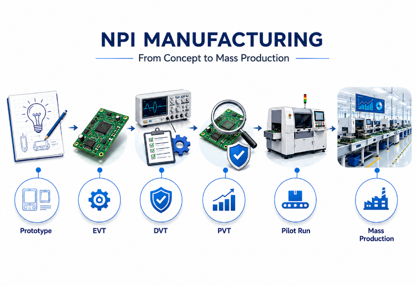
NPI manufacturing is the controlled process of turning a new product design into a repeatable, testable, and production-ready manufacturing process. It identifies design, sourcing, PCB assembly, testing, documentation, and supply-chain risks before higher production volumes make them expensive to correct.
For electronics, effective NPI manufacturing connects DFM, DFA, DFT, EVT, DVT, PVT, pilot production, inspection, testing, and production release to verify manufacturability, process stability, product quality, and readiness for mass production.
What Is NPI in Manufacturing and Why Is It Important Before Mass Production?
A prototype proves that a product can work, but production requires much more: repeatability, controlled documentation, stable sourcing, reliable assembly, and effective testing. NPI provides the structured bridge between those two conditions.
NPI stands for New Product Introduction. In manufacturing, NPI is the structured transition from a developed product design to a stable process that can produce the same product repeatedly under normal production conditions.
A successful prototype is only the starting point. NPI manufacturing determines whether the approved product can be fabricated, sourced, assembled, programmed, inspected, and tested consistently without relying on repeated engineering intervention.
It is important before mass production because it exposes issues that may remain hidden during prototype builds, including PCB fabrication limits, component shortages, unstable assembly processes, weak test coverage, revision mismatches, and supply-chain risks.
Prototype builds often receive more manual attention, engineering support, and flexible sourcing than normal production. These conditions can make a product appear ready even when the manufacturing process is still unstable.
The real output of NPI manufacturing is evidence that both the product and the production process are ready to scale.
What Is the Difference Between NPI and NPD in Manufacturing?
NPI and NPD often overlap during product development, but they solve different problems. NPD focuses on creating the product, while NPI focuses on making that product practical and repeatable to manufacture.
| Category | NPD | NPI |
|---|---|---|
| Full Term | New Product Development | New Product Introduction |
| Main Objective | Develop and validate the product | Prepare it for repeatable production |
| Core Question | Does the product work? | Can it be manufactured consistently? |
| Main Focus | Design and functionality | Manufacturability and process readiness |
| Typical Activities | Circuit, mechanical, and firmware development | DFM, sourcing, validation, and pilot builds |
| Components | Functional suitability | Availability, lifecycle, and alternatives |
| Testing | Engineering verification | Production-ready testing |
| Final Output | Mature product design | Released production process |
The two processes should overlap. If manufacturing feedback begins only after design freeze, PCB construction, component availability, assembly access, testability, or manufacturing cost may force late redesign.
For example, an IC may meet every electrical requirement but be difficult to source at production volume. A PCB may function correctly while using unnecessarily difficult via structures or providing poor test access.
Early NPI manufacturing feedback turns manufacturability into a design requirement instead of a late production problem.
What Are the Main Stages of the NPI Manufacturing Process?
A reliable NPI manufacturing process moves from early feasibility review to progressively more realistic builds. Each stage should remove a defined level of uncertainty before more time, tooling, and production volume are committed.
Step 1: Review manufacturing feasibility. Product requirements, expected volume, PCB technology, materials, components, mechanical interfaces, testing, and schedule are reviewed before major production commitments.
Step 2: Complete DFM, DFA, and DFT reviews. PCB fabrication limits, component placement, assembly access, test points, panelization, and process constraints are checked while design changes remain practical.
Step 3: Build engineering prototypes. Early units verify electrical, mechanical, thermal, firmware, and interface performance. Accepted modifications should be incorporated into controlled design data.
Step 4: Validate the design. EVT and DVT builds verify increasingly mature product configurations and close major engineering and design risks.
Step 5: Validate the manufacturing process. PVT and pilot builds introduce production-intent materials, equipment, tooling, inspection methods, testing, and work instructions.
Step 6: Review production readiness. Open defects, process stability, supply status, documentation, test coverage, revision control, and remaining risks are evaluated.
Step 7: Transfer to routine manufacturing. Production receives the approved files, tooling, programs, quality criteria, and process ownership required for normal manufacturing.
How Do EVT, DVT and PVT Reduce Risks Before Production?
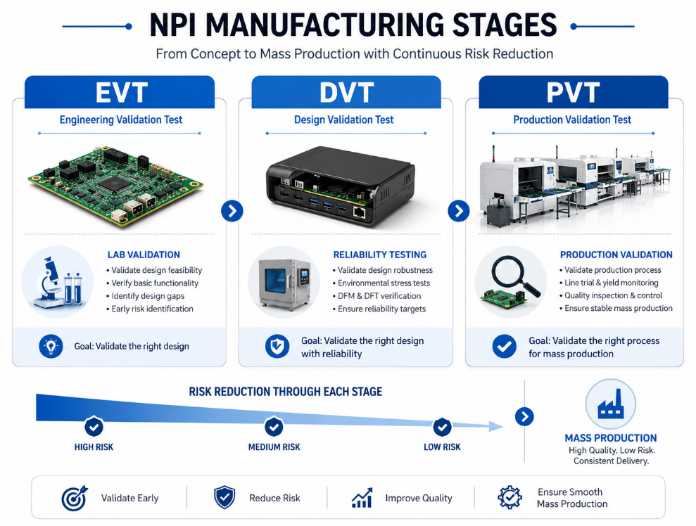
EVT, DVT, and PVT are useful because they separate three different questions: Does the engineering concept work? Is the final design robust? Can the production process build it consistently? Each stage should answer one of these questions before the project advances.
- EVT — Engineering Validation Test: Confirms that the core engineering design works. Typical checks include power rails, communications, thermal behavior, protection circuits, sensors, firmware interaction, and critical interfaces. Accepted PCB or component changes should be incorporated into the controlled design. EVT should close major engineering feasibility risks.
- DVT — Design Validation Test: Verifies the near-final PCB, BOM, firmware, mechanical design, and interfaces against defined requirements. Testing may include electrical performance, thermal margin, mechanical fit, environmental behavior, operating limits, and reliability. DVT should confirm that the design performs consistently with sufficient margin.
- PVT — Production Validation Test: Uses production-intent materials, stencils, equipment programs, fixtures, inspection methods, test systems, and work instructions. It should expose unstable soldering, difficult assembly operations, inadequate test coverage, or excessive operator dependence. PVT should demonstrate repeatable manufacturing without constant engineering support.
Together, EVT reduces engineering uncertainty, DVT reduces design uncertainty, and PVT reduces manufacturing uncertainty before mass production begins.
What Files and Deliverables Are Required During NPI Manufacturing?
NPI manufacturing depends on accurate, revision-controlled data. If the PCB, BOM, firmware, assembly files, and test programs do not describe the same product configuration, even a capable factory can build the wrong version.
- PCB Data: Gerber or ODB++, drill files, board outline, and stack-up.
- PCB Notes: Materials, finish, thickness, tolerances, and special requirements.
- BOM: Manufacturer part numbers, quantities, references, and approved alternatives.
- Pick-and-Place Data: X/Y coordinates, rotation, side, and reference designators.
- Assembly Drawing: Polarity, orientation, and special assembly instructions.
- Mechanical Files: CAD data, dimensions, tolerances, and enclosure interfaces.
- Firmware and Programming Data: Approved firmware revision, settings, and programming method.
- Test Specification: Test conditions, limits, and clear pass/fail criteria.
- Work Instructions: Assembly, inspection, handling, and repair requirements.
- Quality and Traceability Records: Inspection criteria, lot information, serial numbers, and test results.
The most important rule is revision alignment. PCB files, BOM, firmware, assembly data, and test programs must all match the same approved product revision.
How Do DFM, DFA and DFT Reduce Manufacturing Risks During NPI?
Design reviews should address more than whether a product can be built once. DFM, DFA, and DFT check whether it can be fabricated, assembled, and tested repeatedly without unnecessary cost, rework, or diagnostic difficulty.
| Review | Focus | Typical Checks | Main Risk Reduced |
|---|---|---|---|
| DFM | PCB fabrication | Trace/spacing, vias, stack-up, copper, solder mask, panelization | Fabrication defects and low yield |
| DFA | PCB assembly | Footprints, spacing, polarity, thermal balance, access | Assembly defects and rework |
| DFT | Production testing | Test points, programming access, fixtures, test coverage | Undetected failures and slow diagnosis |
DFM improves PCB manufacturability, DFA improves assembly repeatability, and DFT improves defect detection and diagnosis. Together, they prevent design weaknesses from being carried into pilot production and mass production.
How Is NPI Used in Electronics Manufacturing?
Electronics manufacturing combines several dependent processes. NPI manufacturing connects PCB fabrication, component sourcing, PCBA, programming, inspection, testing, and traceability so that issues found in one area are corrected before they affect the next.
- PCB fabrication: Review stack-up, controlled impedance, via technology, solder mask, surface finish, tolerances, and panel construction. Fabrication constraints should be resolved before PCB release.
- Component sourcing: Verify manufacturer part numbers, availability, lifecycle status, lead time, packaging, approved alternatives, and volume support. A complete BOM is not automatically a production-ready BOM.
- PCB assembly: Use SPI, placement results, and reflow feedback to identify solder-paste, package, polarity, spacing, tombstoning, bridging, insufficient solder, and thermal-balance issues. Assembly findings should feed back into the design or process.
- Programming and testing: Define programming access, test points, measurement locations, fixture clearance, and functional-test coverage before layout release. Good DFT improves defect detection and reduces troubleshooting time.
- Inspection: Match inspection methods to actual defect risks. AOI is useful for visible placement and soldering defects, while X-ray is suitable for hidden joints under BGAs, QFNs, and other bottom-terminated packages.
- Traceability: Link the product revision, PCB lot, component lot, firmware version, inspection results, and test records where required. Traceability speeds root-cause analysis when failures occur.
- Corrective action: Assign each significant NPI defect to its true source—design, PCB fabrication, material, supplier, assembly, firmware, fixture, testing, or documentation. Correct the root cause instead of repeatedly repairing the symptom.
How Does NPI Affect the Manufacturing Supply Chain?
A design is not production-ready if key parts cannot support the required volume or schedule. NPI manufacturing therefore reviews the BOM not only for technical correctness, but also for availability, lifecycle, approved sources, and substitution risk.
| Supply Risk | NPI Review | Typical Control |
|---|---|---|
| Long Lead Time | Availability against production schedule | Early purchasing or alternative |
| Single Source | Number of qualified sources | Qualified second source |
| EOL/NRND | Lifecycle status | Replacement plan |
| MOQ | Production purchasing conditions | Volume planning |
| Allocation | Supply-demand exposure | Forecasting and buffer strategy |
| Counterfeit Risk | Procurement channel | Controlled sourcing |
| Package Change | Assembly compatibility | Engineering approval |
| Substitute Part | Form, fit, function | Qualification |
| Supplier Variation | Quality consistency | Supplier control |
| Special Storage | MSL, shelf life, environment | Handling controls |
A component available for 20 prototypes may be difficult to secure for thousands of production units. Availability should be checked against planned production demand, not prototype demand.
Alternative components also require technical review. Package dimensions, pinout, electrical behavior, thermal characteristics, firmware interaction, soldering behavior, and reliability may differ even when headline specifications appear similar.
What Problems Commonly Occur During the NPI Manufacturing Process?
Most NPI problems are not caused by one dramatic failure. They usually come from incomplete data, late changes, weak process margins, sourcing gaps, or unresolved defects that become more expensive as production volume increases.
- Incomplete manufacturing data: Missing PCB notes, component information, assembly instructions, polarity details, or test limits can create avoidable production errors.
- Revision mismatch: PCB, BOM, firmware, stencil, placement data, fixture, or test software from different revisions can produce failures that are difficult to trace.
- Late engineering changes: Changes made after tooling, materials, fixtures, or test systems are prepared can invalidate previous validation work.
- Unresolved DFM issues: Difficult PCB features remain in the design and later reduce fabrication yield, increase cost, or limit supplier options.
- Poor assembly margin: Component spacing, thermal balance, orientation, or access creates unstable SMT or manual assembly.
- Insufficient DFT: Production detects a failure but cannot isolate the cause efficiently because test access or coverage is inadequate.
- Component supply instability: Prototype parts become unavailable, allocated, obsolete, or subject to long lead times at production volume.
- Excessive rework: Boards pass only after repeated adjustment or repair, masking a design or process weakness.
- Weak root-cause analysis: Defects are repaired without correcting their source, allowing the same issue to return.
- Premature production release: Schedule pressure transfers unresolved design, supply, assembly, or test risks into mass production.
Why Can a Successful Prototype Still Fail in Mass Production?
Prototype success and production readiness are not the same. A prototype demonstrates functionality, while mass production requires repeatability across normal variation in materials, equipment, operators, suppliers, and process conditions.
A prototype only proves that the product can work under controlled conditions. Mass production requires the same design to be manufactured repeatedly with stable quality and minimal rework.
Prototype builds often receive extra engineering support, manual adjustment, and detailed inspection. These conditions can hide issues that appear when normal equipment, operators, component lots, and process variation are introduced.
Common causes include PCB and component tolerances, unstable soldering processes, supplier variation, insufficient test coverage, and excessive manual rework. A design that depends on repeated troubleshooting is not ready for volume production.
NPI manufacturing reduces this risk by using pilot builds to verify that the approved PCB, BOM, assembly process, firmware, inspection, and testing can deliver consistent results before mass production begins.
How Should NPI PCB Assemblies Be Inspected and Tested Before Production?
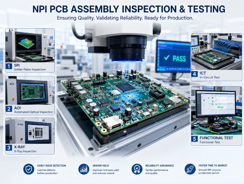
NPI inspection should verify more than whether a finished PCBA works. A reliable test flow checks incoming materials, soldering quality, component placement, hidden joints, electrical performance, firmware, and final functionality before production release.
Step 1: Verify incoming PCBs and critical components. Confirm PCB revision, critical dimensions, surface finish, component part numbers, lot information, packaging, and storage status.
Step 2: Check solder paste with SPI. SPI measures paste position, area, height, and volume before placement, especially for fine-pitch parts, BGAs, and QFNs.
Step 3: Inspect placement and visible solder joints with AOI. AOI can identify missing components, polarity errors, displacement, bridges, and other visible assembly defects.
Step 4: Inspect hidden joints when required. X-ray is useful for BGAs, QFNs, LGAs, and other bottom-terminated packages whose solder joints cannot be evaluated optically.
Step 5: Perform electrical testing. Flying probe or ICT can detect opens, shorts, connectivity faults, and selected component issues. The method depends on test access, board complexity, production volume, and required coverage.
Step 6: Control firmware programming. Use the approved firmware revision, programming procedure, device configuration, and verification method.
Step 7: Perform functional testing. Verify power, communication, control, input, output, and operating functions using measurable pass/fail limits.
Step 8: Complete required reliability testing. Thermal, humidity, vibration, burn-in, mechanical, or other application-specific testing may be required.
Step 9: Analyze defects by root cause. Record defect type, location, process stage, PCB lot, component lot, repair action, and corrective action.
Step 10: Verify corrective actions. Repeat the affected operation after correction. A problem is not closed until evidence shows that the corrective action prevents recurrence.
How Can You Determine Whether an NPI Product Is Ready for Mass Production?
Production release should be based on evidence rather than a target date. The product is ready only when design changes are controlled, pilot builds are repeatable, supply risks are manageable, testing is effective, and routine manufacturing can operate independently.
- Design stability: Major PCB, BOM, firmware, or mechanical changes should no longer occur routinely.
- Controlled manufacturing data: PCB files, BOM, assembly drawings, firmware, work instructions, fixtures, and test specifications must match the same approved revision.
- Repeatable pilot production: Pilot builds should show consistent yield, defect patterns, rework levels, and process behavior. One successful build is not enough to prove production readiness.
- Stable supply chain: Long-lead, single-source, EOL, or allocation-sensitive parts should have approved sourcing plans or qualified alternatives.
- Adequate test coverage: Inspection and functional testing must detect the important failure modes identified during development.
- Controlled rework: Repeated repair, adjustment, or component replacement usually indicates an unresolved design or process issue.
- Closed validation issues: Major EVT, DVT, PVT, and pilot-build findings should be resolved. Lower-risk open items should have defined containment and ownership.
- Production independence: Manufacturing should be able to assemble, program, inspect, test, and document the product without continuous support from the development team.
The strongest release signal is a validated process that can repeatedly produce acceptable units under normal production conditions.
How Does NPI Transfer to Manufacturing Work?
NPI transfer is the point where responsibility moves from development-driven builds to normal production. The handoff should include released product data, validated tooling, approved materials, manufacturing instructions, open-issue status, and clear process ownership.
Step 1: Freeze the production configuration. Confirm the released PCB data, BOM, firmware, mechanical files, assembly instructions, and test requirements.
Step 2: Release production tooling and programs. Stencils, fixtures, placement programs, inspection programs, programming systems, and test equipment should match the approved revision.
Step 3: Release manufacturing instructions. Define critical assembly, handling, inspection, programming, testing, labeling, repair, and traceability requirements.
Step 4: Confirm material readiness. Approved PCBs, components, alternatives, special materials, packaging, and storage requirements should support the planned quantity.
Step 5: Review pilot-build findings. Critical problems should be closed. Remaining lower-risk items should have defined containment, ownership, and corrective actions.
Step 6: Transfer process ownership. Routine production decisions move from the development team to manufacturing, quality, sourcing, and production functions.
Step 7: Monitor early production. Initial mass-production lots should be reviewed for yield, recurring defects, supplier variation, rework, and unexpected test failures.
A successful NPI transfer to manufacturing is reached when normal manufacturing can repeat the validated process without relying on undocumented knowledge or continuous engineering support.
What Should Be Included in a Manufacturing NPI Checklist?
A manufacturing NPI checklist works best as a final release gate rather than an administrative form. It should confirm that design, PCB data, BOM, assembly, testing, supply, quality, and process ownership are all ready before volume production begins.
- Product revision: Confirm the approved PCB, mechanical, firmware, and overall configuration.
- PCB fabrication package: Verify Gerber or ODB++, drill data, stack-up, materials, impedance, finish, and tolerances.
- BOM: Confirm manufacturer part numbers, quantities, approved alternatives, lifecycle status, and availability.
- Assembly data: Verify pick-and-place files, drawings, polarity, orientation, and panel information.
- DFM closure: Confirm major PCB fabrication concerns are resolved.
- DFA closure: Confirm placement, soldering, thermal, access, and assembly risks are controlled.
- DFT closure: Verify test points, programming access, fixture requirements, and test coverage.
- Validation status: Review relevant EVT, DVT, PVT, prototype, and pilot-build findings.
- Inspection plan: Define applicable SPI, AOI, X-ray, electrical, functional, and reliability testing.
- Firmware control: Verify approved firmware and programming instructions.
- Process readiness: Confirm tooling, stencils, fixtures, machine programs, work instructions, and trained personnel.
- Supply readiness: Review lead times, supplier approvals, MOQ, alternatives, and lifecycle risks.
- Quality controls: Define acceptance criteria, nonconformance handling, repair control, and records.
- Traceability: Confirm required PCB lots, component lots, serial numbers, firmware revisions, and test results.
- Production approval: Document remaining risks and authorization to proceed with mass production.
FAQs About NPI Manufacturing
Q1: Who usually owns an NPI project?
A1: Ownership varies by organization. Some companies use an NPI program manager, while others assign responsibility to manufacturing or operations. The critical requirement is one clearly accountable owner who can coordinate design, sourcing, quality, testing, production, suppliers, and stage-gate decisions.
Q2: When should a contract manufacturer become involved in NPI?
A2: A contract manufacturer is most useful before the product design is completely frozen. Early involvement allows PCB DFM, assembly capability, component availability, test access, and manufacturing constraints to influence the product while changes remain practical.
Q3: How long does an electronics NPI project usually take?
A3: There is no universal duration. Timing depends on PCB complexity, tooling, component availability, firmware maturity, validation requirements, test development, and design iterations. Stage entry and exit criteria are more useful than applying one fixed timeline to every project.
Q4: Which KPIs are useful during NPI?
A4: Useful metrics may include first-pass yield, defect rate, rework rate, test failure rate, defect Pareto, supplier defects, engineering-change frequency, and issue-closure rate. Trends across several builds usually provide better evidence than one isolated result.
Q5: What is a golden sample in NPI?
A5: A golden sample is an approved reference unit used for comparison, fixture correlation, functional verification, or training. It can be useful, but it should not replace drawings, specifications, test limits, or controlled manufacturing files.
Q6: How is pilot-build quantity selected?
A6: There is no standard quantity. The appropriate build size depends on product complexity, expected production volume, component cost, failure risk, tooling, and the amount of manufacturing evidence required. The build should be large enough to expose meaningful process variation.
Q7: Should production-intent tooling be used during NPI?
A7: Yes, when tooling can affect product quality. Stencils, fixtures, assembly tools, programming systems, and test fixtures should be evaluated before final production approval. Prototype-only tooling can hide problems that appear only after production starts.
Q8: How should NPI costs be evaluated?
A8: NPI cost includes more than prototype unit price. PCB revisions, engineering reviews, stencils, tooling, fixtures, test development, validation builds, minimum-order quantities, rework, and scrap should also be considered. The lowest prototype price does not necessarily produce the lowest total production cost.
Q9: What records should be retained after NPI?
A9: Useful records include released revisions, approved BOMs, validation results, pilot-build reports, defect data, corrective actions, approved suppliers, test requirements, and production-release approvals. Keeping the evidence behind major manufacturing decisions makes later failure analysis and product changes easier.
Q10: Can NPI be simplified for low-volume electronics?
A10: Yes. Low-volume products may not justify the same automation or tooling used for high-volume production. However, PCB data control, BOM validation, DFM, assembly review, testing, revision control, and supply-chain checks remain important.
Q11: When should an NPI project return to an earlier stage?
A11: A project should move backward when new evidence invalidates an earlier assumption, such as a major PCB redesign, failed reliability test, critical component change, unstable pilot build, or inadequate test coverage. Correcting the problem before scale-up is safer than carrying it into mass production.
Q12: What role does NRE cost play in NPI?
A12: Non-recurring engineering costs can include fixtures, tooling, test development, programming systems, and manufacturing engineering performed before normal production. Higher NRE can be justified when it reduces recurring rework, improves test coverage, or creates a more stable manufacturing process.
Conclusion
Effective NPI manufacturing converts design assumptions into manufacturing evidence before higher volumes magnify design, sourcing, assembly, testing, and quality problems. A product should move into mass production only after manufacturability, assembly capability, testability, supply readiness, process stability, configuration control, and production ownership have been verified.
For a new electronics product, early PCB and PCBA review can prevent costly revisions later in the program. If you are preparing a project for PCB fabrication, PCB assembly, prototype builds, NPI validation, pilot production, OEM/ODM manufacturing, or mass production, contact EBest Circuit for a technical review and quotation: sales@bestpcbs.com.