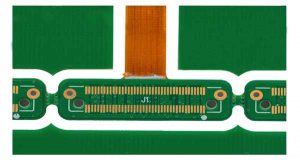
In high-density flexible rigid circuit boards, dense BGA escape routing and a foldable interconnect are one coupled design problem. The via structure that makes routing possible also affects lamination count, dielectric thickness, impedance geometry and the stiffness change at each rigid-to-flex transition. A layout can be electrically complete and still be unsuitable for the installed bend, assembly carrier or qualified fabrication process.
The project should be released in a defined sequence: freeze the installed geometry, approve regional stackups, qualify the microvia architecture, protect bend and transition zones, then build prototypes against measurable acceptance criteria. EBest Circuit can coordinate these decisions across design review, PCB fabrication, component sourcing and assembly without treating the flex section as an afterthought.

What Are High-Density Flexible Rigid Circuit Boards?
One laminated electromechanical circuit: High-density flexible rigid circuit boards combine component-bearing rigid multilayer areas, flexible polyimide interconnects and plated connections in a single manufactured structure. The rigid zones carry dense packages and HDI features; the flex zones replace discrete cables while defining how those rigid zones occupy different planes inside the product.
A rigid-flex board is not the same as an FPC with a stiffener. A stiffener locally supports a flexible circuit but is not normally an electrically interconnected rigid multilayer stack. A rigid-flex construction can terminate layers by region, use blind or buried vias in rigid areas, and maintain selected copper layers through the flex. That regional construction is why one global layer table is insufficient.
High density is also a design condition, not a universal marketing number. It exists when package pitch and I/O count require features such as laser microvias, small capture pads, via-in-pad, blind or buried interconnects, fine line and space, or sequential build-up layers. The density benefit must be balanced against the additional fabrication cycles and the mechanical strain created by copper, coverlay and material transitions.
When Should You Choose a High-Density Rigid-Flex PCB?
Choose it only when density and three-dimensional packaging are both real constraints. A strong use case combines fine-pitch escape routing with a need to fold several functional rigid sections into a repeatable installed shape. If either requirement can be removed, a conventional rigid-flex board, a single rigid PCB or a cable-connected assembly may carry less technical and commercial risk.
| Decision input | Evidence that supports HDI rigid-flex | Reason to retain a simpler architecture |
| Package breakout | Through vias block escape channels or force unacceptable layer count | Standard vias and rules complete routing with margin |
| Installed volume | Rigid functions must occupy multiple planes with controlled fold geometry | All functions fit on one supported rigid board |
| Interconnects | Removing connectors reduces interfaces, assembly operations or mass | Connectors provide needed field replacement or modular service |
| Signal path | A continuous controlled path is easier to manage than several cable transitions | A qualified cable already meets bandwidth and EMC requirements |
| Movement | Static or dynamic bending is dimensioned and testable | Bend radius, torsion, travel or cycle count remains unknown |
| Business case | Reduced enclosure volume and assembly complexity offset higher NRE and process cost | Volume, service strategy or schedule cannot support added qualification |
Run the comparison at assembly level rather than bare-board price. Include connectors, cable procurement, mating operations, inspection access, fastening hardware, rework and field service. HDI rigid-flex often costs more per board, but it can remove interfaces and compress the installed assembly. It is the wrong choice when those system-level gains are not measurable.
How Does EBest Support the Design of High-Density Flexible Rigid Circuit Boards?
EBest converts design intent into a reviewable fabrication proposal before tooling. The input package should include Gerber or ODB++, NC drill data, a regional stackup, fabrication and bend drawings, impedance requirements and a mechanical model. The output should identify assumptions and required changes rather than provide a generic “DFM passed” statement.
| Review zone | EBest review focus | Decision returned to the customer |
| Rigid HDI zones | BGA breakout, microvia span, via-in-pad, capture pads and sequential lamination | Qualified via architecture and required design-rule changes |
| Flex zones | Layer count, copper construction, coverlay, finished thickness and bend use | Proposed material system and bend-rule basis |
| Transitions | Conductor clearance, layer termination, resin flow and stiffener or coverlay edges | Approved boundary geometry and keepout requirements |
| Impedance paths | Trace geometry, dielectric thickness, plane continuity and regional changes | Modeled values and coupon or measurement plan |
| Assembly interfaces | Panel rails, carrier support, connector force and inspection access | Panel and fixture constraints before placement data is frozen |
The verified EBest rigid-flex capability source lists 2–20-layer conventional constructions, ±10% impedance tolerance, and 0.3 mm conventional conductor-to-rigid/flex transition clearance; 0.2 mm is a special capability. These are screening values, not blanket limits. EBest must review the materials, copper weights, layer terminations and HDI structure before confirming manufacturability.
A published minimum line or clearance is not a production-wide routing rule. EBest should mark each feature as standard, conditional or special so procurement can see where cost and schedule risk enter the build.
Planning HDI Stack‑ups, Microvias & Controlled Impedance for High‑Density Rigid‑Flex PCBs
Plan the board as linked regional stackups. The rigid HDI region, flex region and transition region can share selected copper layers while using different dielectric and bonding materials. Each region needs a finished-thickness target, copper definition, reference-plane plan and lamination sequence.
Start the microvia decision with the BGA escape map. Record how many channels are needed per row, which layers receive them and whether a blind via can land on a buried via or must be stacked. Staggered microvias generally avoid a direct vertical stack but consume routing area. Stacked microvias preserve space but increase process dependence and require an explicitly qualified construction. Via-in-pad can improve breakout density, but filling, planarization and surface-flatness requirements must be included in the fabrication note.
| HDI decision | Required input | Failure if treated generically | Evidence before release |
| Microvia span | Start layer, stop layer, dielectric thickness and pad geometry | Poor plating access, weak interface or unqualified depth | Approved stackup and representative microsection plan |
| Stacked versus staggered | Escape density and available landing area | Unnecessary lamination or insufficient routing channels | Fabricator confirmation of the exact build sequence |
| Via-in-pad | Package pitch, pad size, fill and cap requirement | Solder loss, pad depression or assembly void risk | Filled and capped structure specified in the drawing |
| Regional plane continuity | Signal path and return path through each boundary | Reference discontinuity and excess loop area | Layer-by-layer path review across the transition |
| Impedance geometry | Target, tolerance, routed layer, reference and region | Rigid-zone width copied into a thinner flex geometry | Fabricator model plus representative coupon strategy |
Controlled impedance must be modeled with production dielectric thickness and finished copper, not nominal catalog values. The impedance table should separate single-ended and differential nets, identify the routed layer and reference layer, and state whether the target applies in the rigid zone, flex zone or both. Where a signal changes region, verify reference continuity and avoid routing over a plane termination or resin-rich transition.
Before tooling, freeze four linked records: the layer map, the via-span table, the impedance table and the lamination sequence. A change to any one of them can invalidate routing geometry and coupon correlation, so revisions must be reviewed as a set.
How Should Bend Areas and Rigid-to-Flex Transitions Be Designed?
The bend drawing must describe real installed strain. State whether the flex bends once during assembly, moves occasionally for service or cycles continuously in operation. Then dimension bend direction, angle, inside radius, available flex length and any torsion. A radius note without the installed shape is incomplete.
| Design feature | Required treatment | Failure mechanism controlled |
| Trace direction | Cross the bend axis as directly as routing permits | Reduces conductor length exposed to bending strain |
| Trace corners | Use smooth curves and avoid abrupt width changes | Reduces localized strain concentration |
| Via and pad keepout | Keep plated structures and pad edges outside the active bend | Avoids stiffness discontinuity and crack initiation |
| Copper balance | Distribute conductors without creating a locally rigid band | Reduces asymmetric bending and neutral-axis shift |
| Coverlay and stiffener edges | Offset edges from the bend and from one another where required | Avoids a stacked step in stiffness |
| Rigid-to-flex entry | Use approved conductor clearance and strain-relief geometry | Separates copper features from resin and material-edge stress |
Bend radius cannot be copied from another project because total flex thickness, copper type, conductor orientation and layer count change surface strain. Dynamic applications normally need a more conservative construction and a test fixture that reproduces the actual radius, travel and constraint. Static folds still require control: a one-time crease below the approved radius can damage copper before the product leaves assembly.
Teardrops or widened trace entries can soften a geometric transition, but they are secondary controls. They cannot correct a via inside the bend, a stiffener edge on the bend line or a flex tail forced to twist between mounting points. The final release should include a measured bend-zone keepout and a folded-model interference review.
How Are High-Density Flexible Rigid Circuit Boards Prototyped and Verified?
A prototype must prove the proposed process window, not merely produce one functioning unit. For high-density flexible rigid circuit boards, manufacturing coordinates flex-layer imaging, coverlay registration, rigid subassembly preparation, low-flow bonding, sequential lamination, laser drilling, desmear, plating, outer-layer imaging, surface finish, profiling and electrical test. The order changes with the via architecture and layer termination.

| Prototype gate | Question to close | Useful evidence | Release consequence |
| Material receipt | Are the specified flex core, bonding and rigid materials available and approved? | Material identification and approved substitution record | No tooling until material differences are resolved |
| Lamination | Are layer registration, resin flow and flex openings controlled? | Dimensional checks and sampled section review | Adjust tooling or process before repeating build |
| Microvia formation | Does the drilled and plated structure match the approved geometry? | Microsections at representative coupons or locations | Separate design geometry issues from process issues |
| Electrical performance | Do nets, isolation and controlled structures meet requirements? | Electrical-test record and impedance data | Investigate systematic versus isolated deviation |
| Mechanical fit | Does the board fold without interference, torsion or forced crease? | Flat and installed dimensional inspection | Correct outline, flex length or mounting geometry |
| Assembly trial | Can the board be printed, placed, reflowed and inspected with stable support? | Carrier evaluation, X-ray/AOI access and handling record | Revise panel or fixture before volume release |
Build enough samples and coupons to answer the identified risks. A microsection from an easy location does not prove a stacked structure beneath the densest package; a continuity test does not prove bending endurance; a fitted enclosure sample does not prove impedance. Each acceptance method must be tied to the failure mode it can actually detect.
Close prototype findings in a change register. Design changes update the released CAD or drawing. Process corrections update the traveler or qualified parameters. Material substitutions require electrical and mechanical impact review. The volume build should not inherit undocumented prototype exceptions.
How Is High-Density Rigid-Flex PCB Assembly Controlled?
Support the rigid regions without loading the flex. The assembly panel and carrier must hold the printing and placement surfaces flat while keeping vacuum holes, clamps and locating features away from bend and transition zones. If rigid islands sit at different thicknesses or elevations, fixture design must compensate without forcing the panel.
| Assembly step | Control required | Risk if omitted |
| Solder paste printing | Stable underside support and aperture review for fine-pitch pads | Variable paste transfer, bridging or insufficient solder |
| Placement | Rigid-zone datum strategy and flex-safe board handling | Local deflection, placement shift or transition damage |
| Reflow | Material-compatible profile and controlled carrier contact | Warp, delamination, coverlay damage or solder defects |
| Inspection | AOI sight lines and X-ray access beneath hidden joints | Critical defects remain inaccessible or misclassified |
| Depaneling | Supported cutting path with no load transferred through flex tails | Torn transition, cracked trace or edge damage |
| Final folding | Defined fixture, sequence and bend radius | Operator-dependent crease or reversed bend direction |
| Functional test | Fixture access that does not flatten or overbend the assembly | Test-induced damage or nonrepresentative results |
Connector insertion, shield attachment, underfill and rework deserve separate force and thermal review. A connector placed on a small rigid island can transmit insertion force directly into the transition. A rework nozzle can overheat adjacent polyimide or adhesive. These constraints should be visible in the assembly drawing and operator instructions.
The assembly RFQ should include the BOM, centroid or CPL file, assembly drawings, approved alternates, moisture or storage controls, programming requirements and functional-test definition. Without these files, the supplier can quote placement but cannot reliably assess the complete process.
Which Materials and Surface Finishes Suit High-Density Rigid-Flex PCBs?
Select materials as a compatible stack, not an independent list. Flex core, copper, coverlay, bonding film or low-flow prepreg, rigid laminate, stiffener and surface finish must survive the same lamination and assembly temperatures while producing the required thickness, impedance and bend behavior.
| Material decision | Why it matters | Question for supplier confirmation |
| Adhesiveless versus adhesive flex core | Changes thickness, fine-feature capability and flex behavior | Which construction is qualified for the required bend use and copper? |
| Copper construction | Affects ductility, surface profile and repeated bending | Is the copper type appropriate for static or dynamic movement? |
| Coverlay | Protects flex conductors and defines pad openings | Can opening registration and adhesive flow meet the geometry? |
| Low-flow bonding material | Controls resin movement near flex windows | Is it compatible with the rigid laminate and lamination cycle? |
| PI stiffener | Supports connector or component zones without making an active bend rigid | Where will the stiffener edge fall relative to the bend? |
| Rigid laminate | Sets thermal, electrical and dimensional behavior of HDI zones | Are special high-frequency or thermal requirements truly necessary? |
EBest’s capability source includes adhesive and adhesiveless flex cores, coverlay, thermosetting adhesive, PI stiffener, low-flow PP, standard FR-4 and special high-frequency rigid materials. Nonstandard materials can carry procurement, minimum-order and engineering-review conditions. The quotation should identify those conditions rather than silently replace a specified material.
Surface finish follows pad function. ENIG may be considered where flat fine-pitch pads and general solderability are important. OSP, immersion silver, immersion tin, hard gold or another finish can be evaluated for storage, contact wear, wire bonding or assembly compatibility. The drawing should state the required finish and thickness where function depends on it; the supplier should confirm compatibility with fine-pitch assembly and any exposed flex contacts.
How Are High-Density Flexible Rigid Circuit Boards Inspected and Tested?
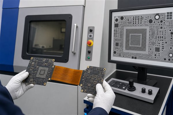
Use a failure-to-evidence matrix. Electrical test, AOI, X-ray, microsection, impedance measurement and bend testing answer different questions. Passing one cannot be used as evidence for another.
| Potential failure | Detection method | What a pass supports | What it does not prove |
| Open or short | Flying probe or fixture electrical test | Continuity and isolation under stated test conditions | Microvia fatigue life or future bend reliability |
| Microvia interface defect | Representative microsection and applicable stress evaluation | Internal geometry and plating condition at sampled structures | Every via on every production board |
| Rigid-to-flex conductor crack | Visual inspection plus monitored bend test | Performance under the defined fixture and cycle | Operation outside that bend radius or temperature |
| Impedance deviation | Representative coupon or specified trace measurement | Electrical response of the measured construction | Return-path quality in an unrelated layout region |
| Hidden BGA solder defect | X-ray inspection | Alignment, bridging and visible void distribution | Joint metallurgy or full functional performance |
| Layer or outline misregistration | Dimensional inspection and cross-section where needed | Geometry against drawing and sampled internal relationship | Dynamic bend endurance |
| Assembly-induced damage | Post-assembly electrical and functional test | Completed assembly behavior at test conditions | Long-term environmental reliability without further testing |
The purchase drawing should define the applicable performance specification, class or acceptance level, coupon requirements, sampling and project-specific tests. IPC-6013 provides a framework for flexible and rigid-flex boards, but it does not replace the need to state bend use, impedance targets, structural options and application criteria.
For volume release, ask for records that match the risk register: electrical-test status for every board, impedance data where controlled structures are specified, dimensional results for critical fold geometry, and sampled microsections for the approved HDI construction. Additional environmental or dynamic testing should reproduce the product requirement rather than use an arbitrary cycle count.
Where Are High-Density Rigid-Flex PCBs Commonly Used?
Use follows geometry and interconnect density, not the industry label alone. Medical, aerospace and industrial products may all justify HDI rigid-flex, but only when their enclosure, package breakout and verification needs align with the construction.
| Engineering scenario | Why HDI rigid-flex may fit | Critical verification | Reason to reject it |
| Compact medical sensing module | Fine-pitch processing and sensor functions occupy different planes | Folded fit, cleanliness, joint inspection and product-specific reliability | A single rigid board fits or serviceability requires connectors |
| Aerospace electronic module | Interconnect mass and connector count must be controlled | Material traceability, vibration and thermal-environment evidence | Qualification burden outweighs packaging benefit |
| Industrial camera or optical unit | Imager, processing and interface boards need fixed alignment | Impedance, folded geometry, thermal path and fixture repeatability | A qualified cable preserves easier module replacement |
| Moving sensor head | Dense electronics connect through a controlled motion path | Representative dynamic bend fixture and monitored continuity | Motion includes uncontrolled torsion or radius variation |
Select HDI rigid-flex only after the package, enclosure, movement and qualification requirements are defined.
Why Choose EBest as Your Rigid-Flex PCB Manufacturer?
Choose a supplier that can close cross-stage decisions. EBest Circuit supports design review, prototyping, volume fabrication, component sourcing and PCB assembly. One team can resolve stackup, panelization, fixture and inspection conflicts before they become separate supplier change requests.
- Regional construction review: EBest can review rigid and flexible layer functions, material interfaces and transition boundaries. The customer should receive an approved stackup with assumptions and special conditions clearly identified.
- HDI process review: EBest can assess the microvia type, sequential build, fine features and via-in-pad requirements. The result should be a qualified structure or a documented redesign request.
- Impedance support: EBest can model production dielectric and copper geometry by region. The customer should receive proposed trace dimensions and an agreed measurement plan.
- Prototype coordination: EBest can coordinate dimensional, electrical, impedance and microsection evidence. The resulting records should map directly to the prototype acceptance matrix.
- Assembly preparation: EBest can review panel support, stencil requirements, inspection access and flex handling. The customer should receive manufacturable panel and fixture requirements before release.
- Material purchasing: EBest can confirm availability, minimum order quantities, approved alternatives and special-process conditions. These commercial constraints should be visible in the quotation.
EBest’s documented capability covers 2–20-layer conventional rigid-flex constructions, conditional HDI structures, ±10% impedance tolerance and defined transition-clearance bands. Final limits depend on the submitted stackup, materials and feature combination.
Ask whether the quotation identifies regional stackups, separates standard from conditional or special features, and names the prototype and production evidence to be delivered. See EBest’s rigid-flex design and prototype process and rigid-flex material selection guidance for the related review steps.
What Files Are Required for a High-Density Rigid-Flex PCB Quote?
A firm quotation requires both flat-board data and installed-use data. Gerber files alone show artwork but do not define how the flex moves, which regional construction is intended or what evidence the buyer expects.
- Gerber or ODB++ and NC drill: Include complete copper, solder mask, coverlay, profile and drill data so the supplier can review features, nets and fabrication requirements.
- Fabrication drawing: State dimensions, tolerances, materials, surface finish and manufacturing notes to define the commercial and quality scope.
- Regional stackup: Identify rigid, flexible and transition layers with finished thicknesses so lamination, material and routing feasibility can be assessed.
- Via-span table: Define start and stop layers, fill or cap requirements and special via structures to establish the HDI build sequence and tooling.
- Bend drawing: Specify bend direction, angle, radius, static or dynamic use and required cycles for flex-material and keepout review.
- STEP model: Provide flat and installed geometry with mounting datums to check interference, flex length and the fold sequence.
- Impedance table: List each net class, routed layer, reference layer, region, target and tolerance for trace modeling and coupon planning.
- Acceptance matrix: Define each test method, sample size, acceptance criterion and required report so quotations and prototype-release evidence can be compared.
- Assembly package: Supply the BOM, CPL, assembly drawings, approved alternates, programming requirements and test plan for the component and PCBA quotation.
Mark open items as requests for engineering proposal instead of leaving them unstated. The supplier can then identify assumptions, options and price effects. An undocumented assumption may produce a lower initial quote, but it usually returns as a stackup change, material delay or tooling revision.
Conclusion
Release the architecture before releasing the artwork. High-density rigid-flex succeeds when the installed shape, regional stackups, microvia structure, transition rules, impedance paths, prototype evidence and assembly support are approved as one system. That discipline prevents a routing solution from becoming a lamination, bending or production problem.
Send your Gerber or ODB++ data, regional stackup, bend drawing, impedance table, BOM, quantity, assembly requirements, programming needs and test plan to sales@bestpcbs.com for an EBest Circuit manufacturability and quotation review.