Choosing FPGA vendors are not simply a comparison of logic cells, speed, and unit price. The selected platform also determines the toolchain, IP licenses, package, power rails, BGA fanout, PCB layer count, sourcing options, and production-test method.
A device may meet the functional specification yet still increase PCB cost or create a supply problem. Before fixing the part number, compare the exact device, package, lifecycle, purchasing channel, and manufacturing impact.
Which Major FPGA Vendors Should Be Shortlisted?
The right shortlist depends on the application. A high-speed networking project, compact industrial controller, low-power sensor, and long-life aerospace product will not use the same selection logic.
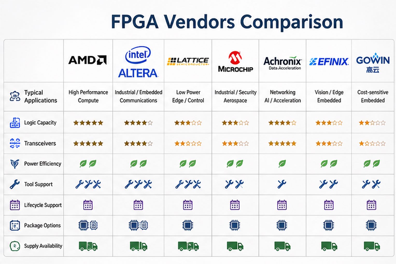
| FPGA vendor | Typical fit | PCB concern |
|---|---|---|
| AMD | Broad portfolio, high-speed and adaptive computing | Dense BGA, power rails, transceivers |
| Altera | Industrial, embedded and high-performance platforms | Tool edition, package and bank planning |
| Lattice | Compact, low-power control and edge applications | I/O capacity and package limits |
| Microchip | Industrial, security and long-lifecycle projects | Programming and device availability |
| Achronix | High-bandwidth acceleration and networking | Power, memory and high-speed routing |
| Efinix | Vision, edge and compact embedded systems | Fine-pitch BGA and HDI risk |
| GOWIN | Cost-sensitive embedded applications | Tool support and approved sourcing |
A practical shortlist normally contains two or three exact devices. Comparing every vendor adds work without improving the final decision.
Which FPGA Vendor Selection Criteria Prevent a PCB Redesign?
Start with mandatory requirements. A device that fails one essential condition should be removed before PCB design begins.
Check:
- Logic, DSP and RAM capacity
- Required speed and temperature grade
- Available user I/O
- I/O-bank voltage compatibility
- Memory and transceiver support
- Package size and ball pitch
- Power rails and sequencing
- Tool and IP availability
- Lifecycle status
- Approved purchasing channels
- Programming and test method
Leave design margin. A device that appears adequate before synthesis may become too small after timing closure, debugging logic, interface changes, and future feature additions.
The exact package matters as much as the FPGA family. Two devices with similar resources may require very different PCB structures because of their ball pitch, number of rows, power-ball distribution, and transceiver placement.

What Should an FPGA Vendor Comparison Table Include?
Compare exact manufacturer part numbers rather than vendor names alone.
A useful comparison should include:
- FPGA family and exact part number
- Package and ball pitch
- Logic, RAM and DSP utilization
- User I/O by bank
- Transceiver count and speed
- Required power rails
- Tool and IP license requirements
- Lifecycle status
- Lead time and approved suppliers
- Estimated PCB layer and via requirements
- Programming method
- Test requirements
Classify each candidate as:
- Pass: no unresolved issue
- Conditional: acceptable after one defined action
- Fail: requires an unacceptable compromise or redesign
This format prevents a low device price from hiding additional costs in PCB fabrication, licensing, regulators, or assembly.
Why Can FPGA Vendors Market Share Mislead Buyers?
FPGA vendor market share can indicate ecosystem size, but it does not identify the best device for a specific product.
Published market-share reports may include different categories, such as:
- Traditional FPGAs
- SoC FPGAs
- CPLDs
- Accelerator cards
- Embedded FPGA IP
- Aerospace devices
- Data-center products
A large installed base can mean more engineers, IP, documentation, and reference designs. However, it does not guarantee that the selected package is available, affordable, easy to route, or suitable for long-term production.
Use market share as background information. The final decision should be based on the exact device, package, toolchain, supply route, lifecycle, and PCB impact.
What Key Features Should You Look for in an FPGA Vendor?
Toolchain support
- Confirm that the selected family is supported by the required tool version and license. Check synthesis, simulation, timing analysis, command-line automation, and project migration.
Usable IP
- Verify that the required USB, PCIe, Ethernet, DDR, MIPI, or other IP supports the selected family and speed grade. Review production licensing before the design depends on it.
Lifecycle information
- Check the lifecycle of the exact ordering code, not only the FPGA family. Package, temperature grade, and speed grade may have different availability.
Programming support
- Define how the FPGA and configuration memory will be programmed during prototypes and volume production. Security features may require controlled files, keys, or dedicated fixtures.
Technical documentation
- Pinout files, power guides, reference schematics, package drawings, IBIS models, and migration information should be available before schematic release.
Are the Best FPGA Vendors Always the Lowest-Risk Choice?
The best FPGA vendor is not always the company with the fastest device or largest market share. It is the platform that leaves the fewest unresolved project risks.
Total platform risk includes:
- Device capacity risk
- Tool and IP risk
- Supply risk
- PCB fabrication risk
- BGA assembly risk
- Thermal risk
- Test risk
A low-cost FPGA can become expensive when it requires:
- Two extra PCB layers
- Laser-drilled microvias
- Filled via-in-pad
- More voltage regulators
- A larger heat sink
- Paid protocol IP
- Another prototype revision
An established platform may cost more per device but reduce development time when the engineering team already has verified IP, constraints, programming tools, and test procedures.
Evaluate total project cost rather than FPGA unit price alone.
When Should You Use FPGA Board Vendors for Prototyping?
FPGA development boards are useful for validating the platform before designing a custom PCB.
They can help verify:
- Toolchain operation
- RTL and timing constraints
- Interface IP
- Embedded software
- USB, Ethernet, PCIe, or memory functions
- Preliminary performance
- Programming flow
However, a development board does not prove:
- Final PCB layer count
- Production power integrity
- BGA escape feasibility
- Thermal performance inside the enclosure
- EMI or EMC compliance
- Final BOM availability
- Volume assembly yield
Before moving to a custom FPGA PCB, freeze the exact part number, package, pin assignments, bank voltages, power architecture, memory topology, clocks, configuration method, and test access.
How Does an FPGA BGA Package Increase PCB Layer Count?
The BGA package can determine whether the PCB uses conventional through vias or HDI structures.
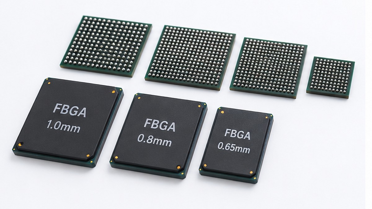
| BGA pitch | Early PCB assessment |
|---|---|
| 1.0 mm | Conventional fanout may be practical |
| 0.8 mm | Smaller drills or tighter routing may be required |
| 0.65 mm | Review microvias and via-in-pad |
| 0.5 mm or below | HDI is often required |
Pitch alone does not determine the layer count. Engineers must also review:
- Number of populated ball rows
- Signal location inside the package
- DDR bus width
- Transceiver count
- Differential-pair routing
- Reference-plane requirements
- Power-plane allocation
- PCB fabrication limits
A preliminary BGA fanout should be completed before the BOM is approved. Otherwise, the selected FPGA may force a more expensive stack-up after layout has started.
What FPGA PCB Design Changes Follow a Vendor Switch?
Changing FPGA vendors usually means more than replacing the footprint.
Review:
- BGA ball map
- I/O-bank arrangement
- Bank voltages
- Core and auxiliary rails
- Power sequencing
- Decoupling layout
- Configuration memory
- JTAG connections
- Clock inputs
- DDR topology
- High-speed interfaces
- Thermal requirements
Even when two devices provide similar resources, their pins may be distributed across different banks. This can change connector placement, power planes, differential-pair routing, and regulator selection.
Treat a vendor switch as a controlled redesign unless package, pin, and electrical compatibility have been confirmed.
How Was a 6-Layer FPGA USB PCB Prepared for 10-Day Delivery?
A customer ordered 1,000 FPGA USB PCBs plus one spare board with controlled impedance, documented testing, and delivery within ten days after EQ approval.
PCB specifications
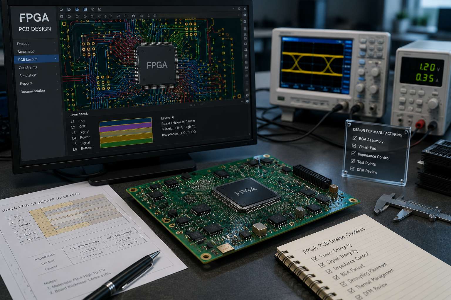
- 6-layer high-Tg 170 FR-4
- Finished thickness: 1.6 mm ±10%
- Outer copper: 1 oz
- Inner copper: 0.5 oz
- Red solder mask and white silkscreen
- ENIG: 1 µin gold
- RoHS and IPC Class 2
- Panelized delivery
Impedance requirements
- 50 Ω single-ended traces on L1, L3, and L4
- 100 Ω differential pairs on L1, L3, L4, and L6
Before production, the engineering review covered the stack-up, reference planes, dielectric thickness, trace geometry, copper compensation, panel design, and impedance coupons.
Every board received electrical testing before shipment. The customer received:
- Electrical test report
- Impedance report
- Production traceability
The project shows our ability to manufacture FPGA USB boards with multilayer construction, mixed impedance requirements, documented testing, and schedule-controlled volume production.
The FPGA model, pin assignment, RTL, and firmware remained customer-defined. Our role was to convert the released files into a repeatable PCB manufacturing process.
What Files Are Required Before FPGA Assembly?
A complete manufacturing package reduces engineering questions and prevents assembly delays.
PCB files
- Gerber or ODB++
- Drill files
- Fabrication drawing
- Stack-up
- Impedance requirements
- Panel instructions
Assembly files
- BOM with manufacturer part numbers
- Pick-and-place file
- Assembly drawing
- Polarity notes
- Approved alternates
Programming files
- Released bitstream
- FPGA and memory part numbers
- Programming interface
- Checksum or verification method
- Security instructions
Test files
- Power-up sequence
- Current limits
- Functional-test steps
- Expected results
- Pass/fail criteria
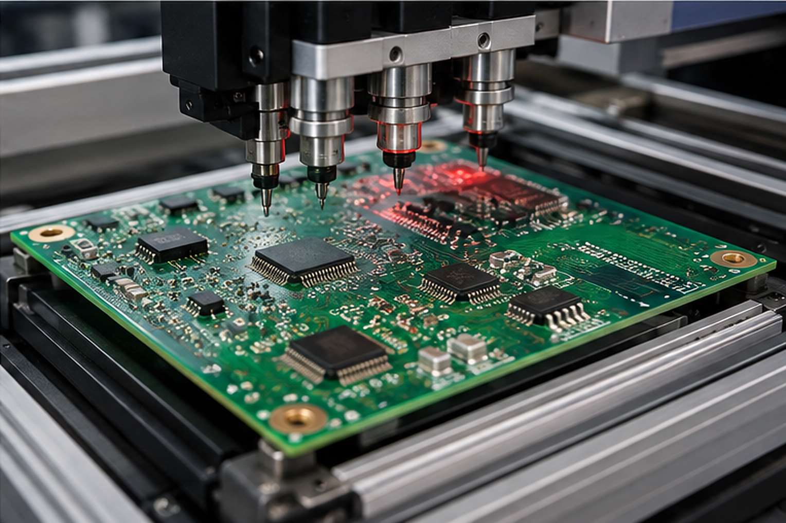

Best Technology supports DFM review, component sourcing, multilayer PCB fabrication, BGA assembly, X-ray inspection, programming, and customer-defined testing. FPGA selection, RTL, firmware, system architecture, and final certification remain the customer’s responsibility.
Preparing an FPGA PCB or PCBA project? Send your Gerber files, BOM, FPGA part number, stack-up, assembly data, and test requirements to sales@bestpcbs.com. Our engineering team will review the BGA fanout, controlled impedance, material availability, component sourcing, assembly access, and test plan before production.