Is RO4450F the right prepreg for your high frequency multilayer PCB stackup? In RF, microwave, and high speed digital boards, RO4450F works as a bonding layer that helps connect layers while keeping dielectric spacing more predictable.
This guide explains what this Rogers bondply is, how thick it is, what Dk value should be used, how it affects impedance control, and what fabrication points should be reviewed before production.
What Is RO4450F Prepreg?
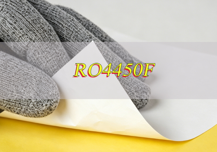
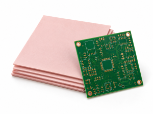
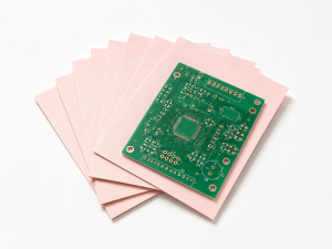
RO4450F is a Rogers high frequency thermoset prepreg, also called bondply. It is used to bond layers together in multilayer PCB structures, especially when RO4000 series laminates are used in RF or microwave boards.
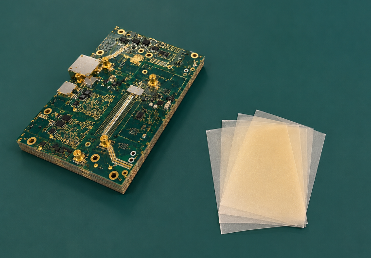
It is different from a copper clad core. A core already has copper on one or both sides, while prepreg is placed between layers during lamination. During pressing, the resin softens, fills around copper patterns, and bonds the stack together.
In practical PCB design, this material is often used with Rogers high frequency laminates such as RO4003C, RO4350B, RO4835, RO4350G2, and RO4000 LoPro materials. RO4400 bondply materials are designed for RO4000 multilayer constructions.
Why Is RO4450F Important in High Frequency Multilayer PCB Stackup?
A high frequency multilayer PCB does not rely only on the core material. The prepreg layer also becomes part of the electrical structure, especially when signal layers are close to reference planes. RO4450F helps define dielectric spacing, bonding quality, and stackup consistency.
In RF and microwave boards, small changes in dielectric height can affect impedance and signal behavior. A stable bonding layer helps the finished PCB stay closer to the intended stackup design after lamination.
RO4450F is also useful when the board has multiple signal layers, copper planes, and via transitions. It helps fill around etched copper patterns while supporting reliable layer adhesion.
For this reason, RO4450F should be reviewed together with the full stackup, including copper weight, dielectric spacing, impedance requirement, via structure, and final board thickness.
How Does RO4450F Work as a Bonding Layer in PCB Stackup?
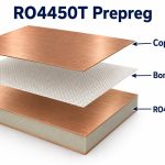
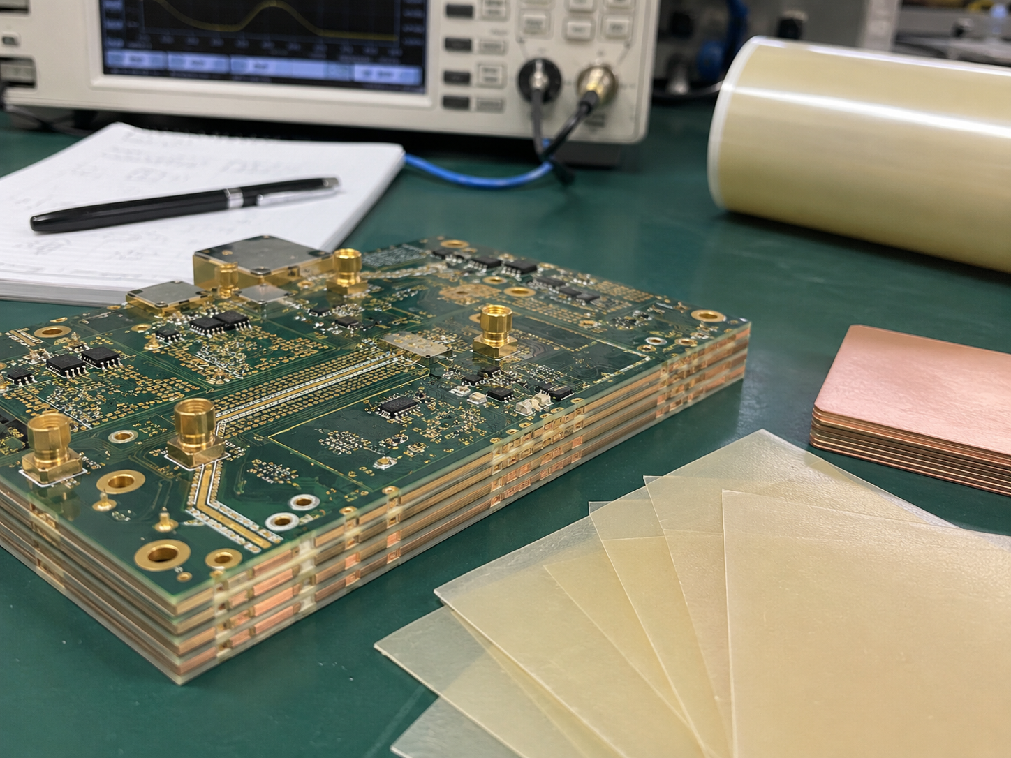
In a PCB stackup, RO4450F is placed between copper layers, high frequency cores, or foil layers before lamination. During pressing, the resin flows around the copper pattern, fills small open areas, and bonds the layers into one multilayer board.
- It bonds PCB layers: It joins high frequency cores, inner copper layers, and foil layers into a stable structure.
- It forms a dielectric layer: After lamination, it becomes part of the dielectric path between conductors.
- It affects pressed thickness: Final thickness depends on copper weight, copper distribution, and lamination conditions.
- It supports copper pattern filling: Resin flow helps fill spaces around etched copper features.
- It influences impedance: Its Dk and pressed thickness should be included in stackup calculation.
- It supports multilayer reliability: Proper bonding helps improve layer adhesion and plated through hole stability.
RO4450F should be treated as both a bonding material and a functional dielectric layer. This makes it important for high frequency multilayer PCB stackup design.
How Thick is Rogers RO4450F?
Rogers RO4450F has a standard thickness of 0.0040 inch, about 0.102 mm. This is the value most designers check first when building a high frequency multilayer stackup.
In a real PCB build, pressed thickness can shift slightly because resin must fill the copper pattern. Copper weight, copper balance, plane coverage, etched area, and press cycle all affect the actual dielectric spacing.
Each 4 mil ply bonds to about 0.004 inch / 0.101 mm when pressed between flat opposing surfaces, while the thickness added to a multilayer construction depends on copper weight and distribution.
What is Dielectric Constant of RO4450F?
The dielectric constant of RO4450F is 3.52 ± 0.05 at 10 GHz in the z direction. This value is important because the bonding sheet is part of the RF dielectric path, not just a mechanical adhesive.
Dk affects signal velocity, controlled impedance, stripline trace width, layer spacing, and coupling between signal layers. If the wrong Dk is used in a field solver, the fabricated board may deviate from the intended impedance.
For accurate stackup review, the Dk value, copper roughness, copper thickness, trace geometry, and pressed dielectric spacing should be checked together.
How Does RO4450F Affect Impedance Control and Signal Stability?
RO4450F affects impedance because its dielectric constant and pressed thickness influence the distance between signal traces and reference planes. When this prepreg is close to an RF trace, it becomes part of the controlled impedance structure.
For stripline routing, the signal trace is usually buried between reference planes. If the bonding layer becomes thinner or thicker after lamination, the impedance value may shift. This is why pressed thickness should be checked before fabrication.
For RF and high speed boards, signal stability also depends on material loss. RO4450F has low loss behavior for high frequency use, but the final result still depends on trace geometry, copper thickness, copper roughness, surface finish, and via design.
Before production, the stackup should be reviewed with the actual dielectric height, Dk value, copper weight, line width, spacing, and impedance target. This helps the finished PCB meet the expected signal behavior more consistently.
Rogers RO4450F Datasheet Overview
The RO4450F datasheet should be read as a design and fabrication reference, not just a material label. The values below summarize important data for this Rogers bondply. Typical values should be verified again when preparing final production documents. Here is a table and PDF of Rogers RO4450F datasheet for your reference:
| Parameter | Rogers RO4450F Typical Value |
|---|---|
| Material Type | High frequency thermoset bondply / prepreg |
| Standard Thickness | 0.0040 in / about 0.102 mm |
| Dielectric Constant | 3.52 ± 0.05 at 10 GHz |
| Dissipation Factor | 0.004 at 10 GHz |
| Thermal Conductivity | 0.65 W/m·K |
| Moisture Absorption | 0.09% |
| Tg | >280°C |
| Td | 390°C |
| CTE | X 19, Y 17, Z 50 ppm/°C |
| Flammability | UL 94 V-0 |
| Lead-Free Process Compatibility | Yes |
These values help designers review Dk, Df, thermal conductivity, Tg, Td, CTE, UL rating, and lead-free compatibility when preparing a high frequency multilayer PCB stackup.
Difference Between RO4450B and RO4450F Prepreg
RO4450B and RO4450F are both Rogers RO4400 series high frequency bondply materials. They are used as bonding layers in multilayer PCB stackups with RO4000 series laminates. The main difference is not their basic function, but their available thickness, dielectric value, and resin flow behavior.
| Item | RO4450B | RO4450F |
|---|---|---|
| Material Family | Rogers RO4400 series bondply | Rogers RO4400 series bondply |
| Material Type | High frequency thermoset prepreg | High frequency thermoset prepreg |
| Main Function | Bonding layer for RO4000 multilayer PCB constructions | Bonding layer for RO4000 multilayer PCB constructions |
| Standard Thickness | 0.0036 in / 0.091 mm and 0.0040 in / 0.101 mm | 0.0040 in / 0.101 mm |
| Dielectric Constant | 3.30 ± 0.05 or 3.54 ± 0.05 at 10 GHz, depending on thickness | 3.52 ± 0.05 at 10 GHz |
| Dissipation Factor | 0.004 at 10 GHz | 0.004 at 10 GHz |
| Thermal Conductivity | 0.60 W/m·K | 0.65 W/m·K |
| Tg | >280°C | >280°C |
| Td | 390°C | 390°C |
| Z-Axis CTE | 60 ppm/°C for 0.0036 in version; 50 ppm/°C for 0.0040 in version | 50 ppm/°C |
| Flow Behavior | Standard RO4400 bondply flow behavior | Improved lateral flow capability |
| Fill Requirement | Suitable for standard RO4000 multilayer bonding structures | More suitable when the stackup has difficult fill requirements |
| Sequential Lamination | Supported by RO4400 bondply family | Supported by RO4400 bondply family |
| Lead-Free Process | Compatible | Compatible |
| Typical Use Direction | Existing or previously approved stackups | New stackups or designs needing better resin flow |
| Replacement Advice | Keep using it when the stackup is already verified | Review when better filling behavior is needed |
The material data shows that RO4450B and RO4450F share the same high frequency bondply family, similar loss factor, high Tg, lead-free compatibility, and RO4000 multilayer compatibility. RO4450F is mainly highlighted for improved lateral flow capability, which makes it useful for new multilayer stackups or structures with more demanding fill requirements.
What Applications Use Rogers RO4450F PCB Material?
This prepreg is mostly used where the board needs multilayer construction and stable high frequency behavior. It is a practical fit for RF, microwave, and high speed interconnect boards that use Rogers RO4000 series cores.
- RF communication modules: Used where low loss paths and controlled impedance are needed.
- Microwave PCB assemblies: Supports multilayer routing and stable dielectric spacing.
- Power amplifier PCBs: Helps create reliable RF stackups with controlled layer bonding.
- Antenna module PCBs: Useful when the antenna feed structure needs repeatable dielectric behavior.
- Small cell and DAS boards: Fits compact communication hardware with multilayer RF routing.
- Backhaul radio boards: Supports high frequency paths in outdoor or telecom equipment.
- Radar PCBs: Used in multilayer RF boards where material consistency matters.
- Test and measurement boards: Helps maintain signal behavior in precision RF test hardware.
- Mixed material multilayer PCBs: Suitable when high frequency cores and other materials must be laminated together.
Stackup and Lamination Considerations for RO4450F PCB Fabrication
A good build starts with a clear stackup, not with material selection alone. The prepreg must match the copper pattern, impedance target, via structure, and press cycle.
- Copper thickness: Heavy inner copper needs careful fill review. RO4400 bondply materials can fill up to 0.0018 inch of total copper thickness, with more bondply needed when fill exceeds that range.
- Copper distribution: Large plane areas and open etched areas can create uneven resin flow. Copper balance helps pressed thickness remain more consistent.
- Layer count: Higher layer count boards may need a more detailed lamination plan, especially with buried copper and mixed materials.
- Pressed thickness: Do not use nominal thickness alone for final impedance. Pressed dielectric height should be checked against copper pattern and fabrication tolerance.
- Impedance coupon: RF and high speed boards should include a coupon plan when controlled impedance is required.
- Inner layer treatment: Metal surfaces should receive a suitable oxide or oxide alternative treatment for better adhesion.
- Press profile: A reduced viscosity range around 100°C to 120°C and bonding pressures commonly between 400 and 750 PSI may be used depending on fill needs.
- Drilling and desmear: Multilayer RO4000 constructions may require desmear after drilling, while etchback of core and prepreg layers is not recommended.
- Surface finish: ENIG, immersion silver, OSP, and other finishes should be selected according to RF performance, soldering needs, and storage conditions.
- Batch repeatability: For production, stackup, material lot control, lamination records, impedance data, and inspection results should be documented.
Why Choose EBest for RO4450F Multilayer PCB Fabrication?
High frequency multilayer fabrication needs more than access to Rogers materials. It needs stackup review, DFM checking, impedance control, lamination control, drilling quality, inspection, and clear communication before production. Here are reasons why choose EBest for RO4450F multilayer PCB fabrication:
- Rogers high frequency PCB fabrication: Support for RF, microwave, antenna, radar, communication, and high speed multilayer boards.
- Stackup review before production: Review dielectric spacing, copper thickness, layer order, impedance targets, and final board thickness.
- DFM checking: Check manufacturability risks in spacing, via structure, copper balance, annular ring, solder mask, and panel layout.
- Impedance control: Support microstrip, stripline, differential pair, and RF trace requirements.
- Mixed material PCB capability: Support Rogers materials with other PCB materials when the structure requires it.
- Inspection and testing: AOI, electrical test, dimensional checks, and quality records for controlled production.
- Prototype and batch support: Support small quantity validation and later volume production under the same fabrication control path.
- PCBA service availability: PCB fabrication can be combined with component sourcing, SMT assembly, testing, and box build service when needed.
FAQs About Rogers RO4450F Prepreg
Q1: Can RO4450F be laminated with RO4350B or RO4003C?
A1: Yes. RO4450F is commonly used with Rogers RO4000 series high frequency laminates, including RO4350B and RO4003C. The final stackup should still be reviewed according to layer count, copper weight, dielectric spacing, and impedance target.
Q2: When should this Rogers bondply be considered for an RF multilayer PCB?
A2: It is suitable when the board needs stable dielectric spacing, controlled impedance, low signal loss, and reliable multilayer bonding. It is often used in RF, microwave, antenna, radar, and high speed communication boards.
Q3: Does one ply always provide enough resin fill?
A3: Not always. Resin fill depends on copper thickness, copper pattern density, open area, and lamination pressure. For heavy copper or uneven copper layouts, the stackup may need extra review before fabrication.
Q4: Will the final pressed thickness match the nominal thickness exactly?
A4: The nominal thickness is a starting value. The final pressed thickness may change slightly after lamination because resin flows around etched copper patterns. For controlled impedance boards, the calculation should use the reviewed fabrication stackup instead of only the nominal material value.
Q5: Can RO4450F replace RO4450B directly?
A5: It should not be replaced directly without review. RO4450F has improved lateral flow behavior, but replacement still needs checking for Dk, thickness, resin flow, impedance, and previous production approval.
Q6: Is this bondply suitable for sequential lamination?
A6: Yes. RO4400 series bondply materials can be used in multilayer structures that may involve sequential lamination. The press cycle, inner layer treatment, and total thermal history should be reviewed before production.
Q7: What may cause impedance deviation in this type of stackup?
A7: Common causes include pressed dielectric thickness variation, copper thickness tolerance, copper roughness, trace width deviation, resin flow change, and reference plane distance. A controlled stackup and impedance coupon can help reduce these risks.
Q8: Is standard FR4 prepreg a good substitute in RF layers?
A8: Usually not for controlled RF layers. Standard FR4 prepreg has different dielectric behavior and higher loss at high frequency. For RF paths, the bonding material should match the required Dk, Df, dielectric thickness, and impedance structure.
Q9: What should be prepared before requesting fabrication?
A9: Prepare Gerber files, stackup drawing, material callout, copper weight, finished board thickness, impedance requirements, surface finish, via structure, and estimated quantity. These details help the factory review manufacturability faster.
Q10: Can EBest support both PCB fabrication and assembly for this material?
A10: Yes. EBest can support Rogers high frequency PCB fabrication, DFM review, stackup checking, impedance control, PCB manufacturing, component sourcing, SMT assembly, testing, and production follow up.
Get a Fast Quote for RO4450F High Frequency PCB
Planning a Rogers high frequency multilayer PCB build? Send your Gerber files, stackup requirement, copper weight, impedance target, surface finish, and quantity to EBest for a fast fabrication review. Our team can support high frequency PCB fabrication, DFM checking, multilayer stackup review, impedance control, PCB manufacturing, PCB assembly, component sourcing, and production testing. Contact us at sales@bestpcbs.com to get a quotation for your next RF or high speed PCB project.
You may also like

Tags: ro4450b vs ro4450f, ro4450f datasheet, ro4450f dielectric constant, ro4450f prepreg, ro4450f thickness, rogers ro4450f