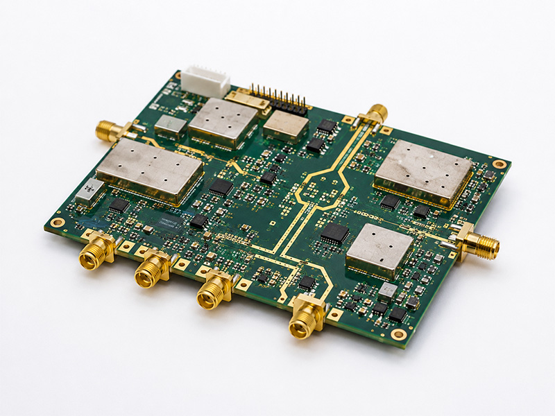
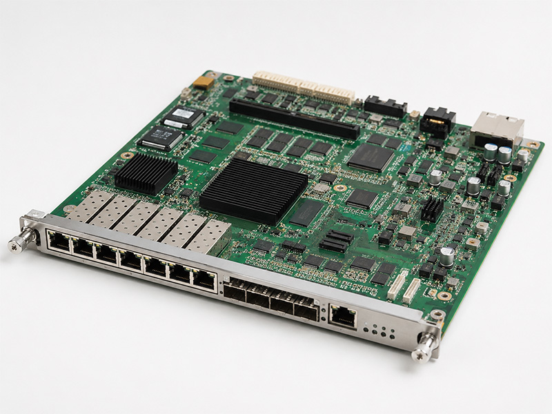
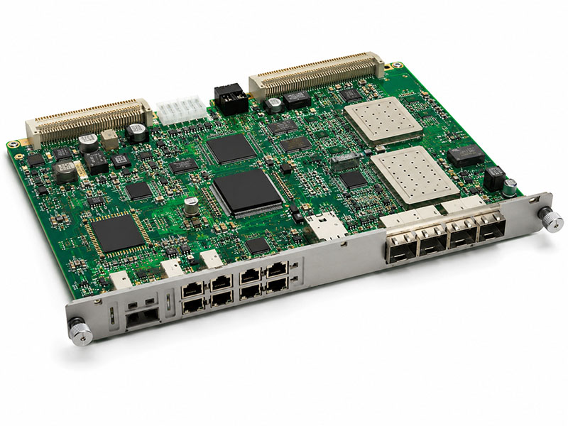
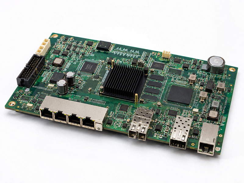
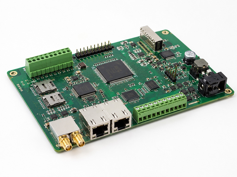
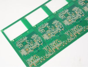
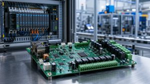
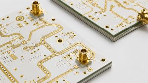
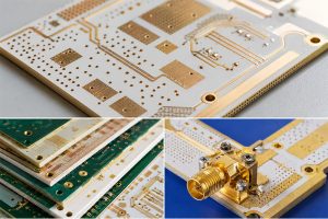
Telecom PCB manufacturing services cover the fabrication, assembly, inspection and testing decisions needed for communication equipment boards, especially when RF behavior, signal integrity, material choice, shielding, thermal load or production repeatability matters. The right supplier should help the buyer review the board as an engineered communication product, not only quote a generic PCB.
This guide explains how to compare telecom PCB suppliers, what the current supplier comparison landscape show, which technical requirements should be clarified, and what files to send for a useful RFQ.
Telecom PCB Manufacturing Services at a Glance
A telecom PCB service should connect bare board fabrication, DFM review, assembly planning, RF-related checks, testing expectations and quote assumptions. The exact requirement depends on whether the board is a base station module, router board, antenna interface, IoT gateway, fiber equipment board, power board or control PCB.
Area
What to confirm
Why it matters
Electrical behavior
Controlled impedance, RF paths, return paths and signal integrity needs
Telecom boards can fail even when the bare board passes simple continuity tests.
Materials
FR-4, high-frequency material, hybrid stackup or project-specific laminate
Material choice affects loss, stability, cost and manufacturability.
Assembly
BOM, CPL, shielding, connectors, polarity and inspection access
RF modules, connectors and shielding parts can drive assembly risk.
Testing
Electrical test, AOI, X-ray if needed, functional or RF test responsibility
The buyer must know what the supplier can verify before shipment.
Is Your Telecom PCB Project Exposed to RF, Thermal or Assembly Risk?
Telecom PCB buyers need supplier review that connects RF material, stackup, impedance, thermal load, assembly and testing.
Customer Pain Point
Project Risk
How bestpcbs Helps
RF material and stackup are not reviewed together
Signal behavior may not match the application requirement
bestpcbs asks for frequency range, stackup notes, material expectations and impedance targets before production.
Thermal and power requirements are unclear
The board may work in prototype but struggle in operating conditions
bestpcbs reviews copper, board structure, component placement and thermal notes during DFM review.
Assembly data is separated from fabrication data
Connectors, shields or RF components may create handling and inspection risks
bestpcbs checks BOM, CPL, assembly drawings and polarity notes when PCBA is required.
Test requirements are not stated early
The buyer may not get the right verification for telecom use
bestpcbs confirms electrical, impedance or customer-defined tests during RFQ preparation.
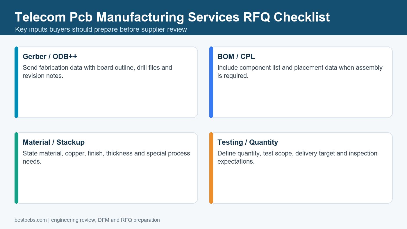
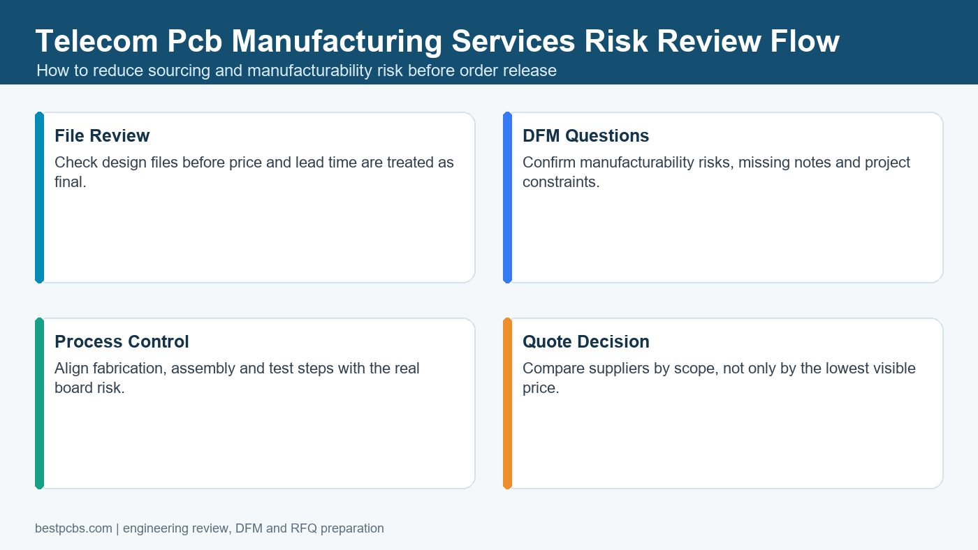
telecom pcb manufacturing services RFQ checklist for supplier review.telecom pcb manufacturing services risk review flow before production.
Telecom PCB Buyer Priorities Before Supplier Selection
Telecom PCB buyers should confirm RF behavior, stackup, material needs, impedance control, thermal load, assembly requirements and test expectations before selecting a supplier. Communication equipment can be sensitive to material and layout assumptions.
Provide frequency range, impedance targets, stackup notes, RF layout constraints, BOM, CPL and testing requirements early. A supplier review before production helps reduce delays caused by missing material, assembly or inspection details.
What Makes Telecom PCBs Different?
Telecom PCBs are different when the board carries RF signals, high-speed data, stable clocking, dense connectors, shielding, thermal load or long production life requirements. Not every telecom board is high-frequency, but every telecom project should identify which sections are electrically sensitive.
A simple control board inside communication equipment may use standard PCB rules. A board with antennas, RF front ends, filters, high-speed interfaces or impedance-controlled lines needs closer review. For RF-specific buying questions, the RF PCB manufacturer RFQ guide is a useful supporting reference.
Materials and Stackup for Telecom PCB Projects
Material and stackup should be selected after the signal behavior, thermal load, layer count, impedance needs and assembly process are understood. Standard FR-4 may be appropriate for many control and power areas, while RF or high-speed sections may need a different laminate or hybrid construction.
Buyers should send the target stackup, copper weight, impedance requirements, operating frequency if relevant, board thickness, surface finish and any thermal notes. Exact material capability and special process limits must be confirmed from the latest project data before order release.
RF, Impedance and Signal Integrity Checks
RF and impedance requirements should be stated in the fabrication notes instead of left for the supplier to infer from the Gerber files. Missing impedance targets, reference planes, material assumptions or test methods can create quote changes and production uncertainty.
State controlled impedance values and tolerance requirements if applicable.
Provide stackup targets and dielectric material expectations.
Identify RF paths, antenna areas, ground references and shielding zones.
Clarify whether the supplier is responsible for impedance coupon testing.
Separate ordinary digital/control areas from RF-sensitive sections.
Telecom PCB Assembly and Component Sourcing
Telecom PCB assembly should be planned with connectors, shielding, RF modules, fine-pitch components, thermal parts and component availability in mind. A bare PCB quote does not answer whether the final board can be assembled cleanly.
If the project needs mounted components, prepare BOM, CPL, assembly drawing, polarity notes, approved substitutes and any testing instructions. The PCBA service is the right internal path when fabrication, assembly and sourcing need to be reviewed together.
DFM Review Before Telecom PCB Production
DFM review should catch manufacturability risks before the telecom board is quoted as a production job. This includes drill-to-copper clearance, solder mask openings, fine-pitch pads, via design, copper balance, controlled impedance notes, panelization and assembly access.
For production-oriented layouts, compare the board against a PCB design and manufacturing DFM guide before release. If RF or high-speed rules are unclear, label them as targets and ask the supplier to confirm what can be manufactured and tested.
Testing and Inspection for Telecom PCBs
Testing should be defined before the order because telecom boards may need more than a standard bare-board electrical test. A supplier can verify open/short conditions, visual quality and assembly defects, but RF performance or functional behavior may need buyer-supplied fixtures and acceptance rules.
Test or inspection
What it checks
Buyer input needed
Electrical test
Bare board opens and shorts
Gerber, netlist and test expectations
AOI / visual inspection
Soldering, placement and visible defects
Assembly files, polarity and acceptance criteria
Impedance test
Controlled impedance coupon or trace behavior
Target values, tolerance and stackup
Functional or RF test
Board-level communication or signal performance
Fixture, firmware, procedure and pass/fail limits
How to Compare Telecom PCB Suppliers
Compare suppliers by whether they can discuss the actual telecom risk in the board, not only by whether they list PCB manufacturing services. A good supplier should ask about stackup, impedance, materials, assembly files, test method and delivery requirements.
Can the supplier review RF or impedance notes before quote approval?
Can they support both PCB fabrication and assembly if required?
Do they identify special materials or processes that need confirmation?
Do they explain what testing is included and what requires buyer fixtures?
Can they quote prototype, low-volume and repeat production needs separately?
What Determines Telecom PCB Manufacturing Cost?
Telecom PCB cost is shaped by material, layer count, impedance control, board size, copper, finish, connector complexity, assembly method, testing, quantity and delivery expectations. A lower quote may be valid for a simple control board but incomplete for an RF or high-speed communication board.
For cost planning, compare telecom requirements with the custom PCB cost guide, then ask suppliers to quote the same stackup, finish, testing and assembly scope.
RFQ Checklist for Telecom PCB Manufacturing Services
A telecom PCB RFQ should include enough detail for the supplier to identify fabrication, assembly and testing risk before committing to price and lead time. Short requests such as “telecom PCB quote” usually lead to follow-up questions.
Gerber or ODB++ files, drill data and fabrication drawing.
Layer count, stackup, material, copper, thickness and surface finish.
Controlled impedance values, RF notes or high-speed constraints if applicable.
BOM, CPL, assembly drawing, polarity notes and substitute rules for PCBA.
Quantity, prototype or production stage, target lead time and delivery destination.
Electrical test, impedance test, functional test or RF test expectations.
Frequently Asked Questions About Telecom PCB Manufacturing
Are all telecom PCBs high-frequency PCBs?
No. Some telecom boards are power, control or interface boards using standard materials. Others include RF or high-speed sections that need special stackup, material and impedance review.
Can one supplier handle telecom PCB fabrication and assembly?
Yes, if the supplier supports both PCB manufacturing and PCBA. A combined review can reduce handoff mistakes between Gerber files, BOM, CPL, assembly notes and testing requirements.
What should I send for a telecom PCB quote?
Send Gerber or ODB++, drill files, stackup, material, impedance notes, finish, quantity and delivery target. For assembly, also send BOM, CPL, drawings, polarity notes and test requirements.
How do I avoid quality problems in telecom PCB sourcing?
Define the sensitive circuit areas, state material and test assumptions, request DFM review, and confirm what the supplier can actually verify before shipment.
Final RFQ Recommendation
Before choosing telecom PCB manufacturing services, identify whether the board is mainly standard fabrication, RF/high-frequency, high-speed, assembly-heavy or test-heavy. The supplier can quote more accurately when the technical risk is visible.
For a telecom PCB fabrication or assembly quote, send your Gerber or ODB++ files, drill data, stackup, impedance notes, BOM, CPL, assembly drawing, quantity, material expectations, surface finish, testing requirements and target lead time to sales@bestpcbs.com. The Best Technology / bestpcbs team can review the project files and confirm what needs project-specific checking before production.
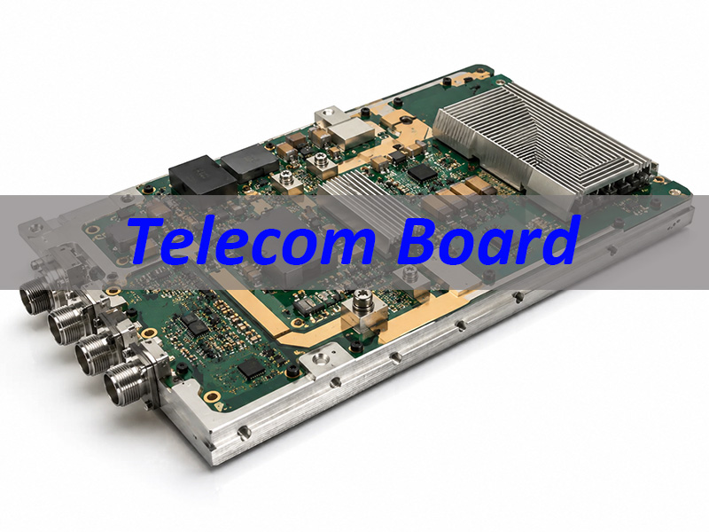
A telecom board supports signal transfer, power control, data exchange, and network communication inside telecom equipment. It may look like a common PCB, but it often needs tighter control over layout, materials, impedance, assembly, and testing. Therefore, engineers and buyers should understand how each manufacturing step affects final performance. In this guide, we explain what a telecom board is, where it works, what layout details matter, how manufacturers build it, and how EBest Circuit supports telecom PCB fabrication and assembly from prototype to production.
What Is a Telecom Board?
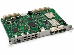
A telecom board is a printed circuit board for communication equipment. People may also call it a telecommunications board, telecom PCB, or telecom circuit board.
In simple terms, this board helps electronic devices send, receive, process, or control communication signals. These signals may come from RF modules, optical devices, routers, switches, gateways, or wireless systems.
Unlike a simple control board, a telecom board often needs better signal control. For example, it may need controlled impedance, stable grounding, low signal loss, clean power delivery, or high-speed data routing. Also, many telecom products run for long hours. So, the board must support stable operation over time.
A telecom board can use different structures. It may be a standard FR4 PCB, a high-frequency PCB, a multilayer PCB, a rigid-flex PCB, or a metal core PCB. The right choice depends on the product design, working frequency, heat level, size, and assembly needs.
In real production, a good telecom board does not depend on one factor alone. Instead, it comes from a full process. Layout review, material selection, stack-up control, PCB fabrication, component sourcing, SMT assembly, inspection, and testing all matter.
Item
What It Means for a Telecom Board
Signal transmission
The board must support clean and stable signal paths.
Power control
The board must deliver steady power to ICs, RF parts, and modules.
Material choice
The laminate must match frequency, loss, heat, and cost needs.
Assembly quality
Components must be placed and soldered with good process control.
Testing
Electrical, impedance, AOI, X-ray, and functional tests help confirm quality.
Telecom Board vs Telecommunications Board: Are They the Same?
In most PCB manufacturing contexts, telecom board and telecommunications board mean nearly the same thing. Both refer to circuit boards for communication products.
However, the word “board” can create confusion. In some searches, a telecom board may mean a cable installation backer board. In other searches, it may mean a company board of directors or a telecom job board. Because of this, a PCB article should make the meaning clear from the beginning.
In this article, a telecom board means a PCB or PCBA for electronic communication equipment.
Term
Common Meaning
In This Article
Telecom board
A short term with several possible meanings
A PCB or PCBA used in telecom equipment
Telecommunications board
A more formal term
A circuit board for communication systems
Telecom PCB
A clear manufacturing term
A bare printed circuit board for telecom use
Telecom PCBA
An assembled board
A telecom PCB with components mounted on it
The shorter term telecom board sounds more common and easier to search. The term telecommunications board sounds more formal. Still, both can describe the same product type when we talk about PCB manufacturing.
For buyers, the name matters less than the actual requirement. A real telecommunications board must support stable signal paths, reliable solder joints, suitable materials, and repeatable production quality. Therefore, the focus should stay on engineering and manufacturing details.
What Are Telecom Circuit Boards Used For?
Telecom circuit boards work in many communication systems. Some boards process high-speed digital signals. Some handle RF signals. Others manage power, interfaces, control logic, or network connections.
Application
Common Board Function
Typical PCB Requirement
5G and wireless equipment
Signal transmission, antenna control, RF processing
For example, 5G modules, antenna systems, repeaters, base station parts, and wireless transmission devices often need telecom circuit boards. These boards may require controlled impedance, low-loss materials, and stable copper patterns.
Routers and switches also need telecom boards. These boards support data transfer, power regulation, interface control, and signal processing. Also, they often include BGA chips, Ethernet interfaces, fine-pitch components, and high-speed signal lines.
In industrial communication, gateway boards connect machines, sensors, PLCs, and cloud systems. Therefore, their boards often combine communication interfaces, power circuits, isolation areas, and control units.
As a result, telecom circuit boards cover a wide range of products. However, they share one common goal: they must help communication signals move with stability and low interference.
What Telecom PCB Layout Factors Affect Signal Integrity?
Telecom PCB layout has a strong effect on signal quality. EBest Circuit does not position itself as a full circuit design company. However, we can support layout review, DFM suggestions, stack-up review, impedance coordination, and manufacturability checks.
Before production, engineers should check several layout details.
Split planes, via stitching, reference layer design
RF trace clearance
It reduces noise and coupling.
Distance from power, clock, and digital lines
Via placement
It can affect RF and high-speed signals.
Via count, via position, via type, stub length
Power layout
It supports stable IC operation.
Decoupling placement, power plane design
Assembly clearance
It reduces SMT risk.
Component spacing, pad size, solder mask clearance
Many telecom boards need controlled impedance. This is common in RF lines, Ethernet lines, differential pairs, and high-speed digital interfaces. Trace width, spacing, copper thickness, dielectric thickness, and material type all affect impedance. Therefore, the layout and stack-up should match each other.
Grounding also deserves attention. A clean return path helps signals move with less noise. If a signal crosses a split ground plane, the return path may become unstable. So, ground plane continuity should be checked early.
RF traces need enough distance from noisy power lines, clock signals, and digital circuits. In many telecom PCBs, engineers also use via fences, shielding areas, or grounded copper to improve isolation.
A layout may look perfect in design software. However, real PCB production has tolerances. Etching, drilling, plating, solder mask registration, and lamination can all change final results. Therefore, DFM review helps reduce risk before fabrication.
At EBest Circuit, our layout-related support focuses on practical production checks. We help customers review manufacturability, stack-up feasibility, impedance needs, soldering risks, and assembly clearance.
How Do Telecom Board Manufacturing Processes Support Stable Signal Transmission?
Telecom board performance does not come from layout alone. The manufacturing process also plays a major role. Even small process changes can affect impedance, signal loss, solderability, and long-term stability.
The stack-up defines layer order, dielectric thickness, copper thickness, and reference planes. For controlled impedance boards, stack-up control is very important. EBest can review the stack-up and match it with material and impedance needs.
Signal traces must stay close to the design target. If etching changes the trace width too much, impedance may shift. Therefore, manufacturers need stable imaging and etching control.
Vias also matter. Multilayer telecom boards often include many vias. Accurate drilling helps keep layer connections stable. Also, good hole wall preparation supports reliable copper plating.
Surface finish selection affects assembly quality. Telecom boards may use ENIG, OSP, immersion silver, HASL, or other finishes. ENIG often works well for fine-pitch components and BGA assembly. However, the best finish depends on the product, storage needs, and assembly process.
In short, stable telecom board manufacturing needs tight process control. Each step should support the electrical goal of the board.
What Materials Are Best for High-Frequency Telecom Circuit Boards?
Material choice has a direct effect on telecom board performance. Different products need different materials. Therefore, engineers should not choose a material only by price or habit.
Material Type
Best-Fit Telecom Application
Main Advantage
Standard FR4
Control boards, network boards, low-to-mid frequency boards
Mature process and cost control
High-Tg FR4
Multilayer boards and higher-temperature products
Better thermal stability
Rogers material
RF, microwave, antenna, and high-frequency boards
Lower loss and stable dielectric behavior
PTFE-based laminate
Low-loss RF and microwave boards
Good high-frequency performance
Metal core PCB
Power modules and heat-generating telecom boards
Better heat spreading
Hybrid stack-up
Boards with both RF and digital sections
Balance between cost and performance
FR4 works well for many standard telecom control boards, digital boards, and network interface boards. It offers good cost control, easy sourcing, and mature processing.
High-Tg FR4 supports better thermal stability than standard FR4. It suits multilayer telecom boards, dense assemblies, and products with higher working temperatures.
Rogers laminates are common in RF, antenna, microwave, and high-frequency telecom PCBs. These materials offer more stable dielectric performance and lower signal loss than standard FR4 in many high-frequency designs.
Some RF and microwave boards use PTFE-based materials. These materials can support low-loss signal transmission. However, they need careful fabrication control because they behave differently from FR4.
Some telecom modules generate more heat. For example, power modules or RF amplifier boards may need better thermal paths. In these cases, aluminum or copper base PCBs can help spread heat.
Also, some telecom boards combine FR4 and high-frequency materials. This can reduce cost while keeping RF layers stable. As a result, hybrid stack-ups often work well when only part of the board needs high-frequency performance.
When choosing materials, engineers should review dielectric constant, dissipation factor, copper foil type, Tg, CTE, thermal conductivity, thickness tolerance, and supply stability.
How Does Custom Telecom PCB Assembly Work at EBest?
Telecom PCB assembly at EBest follows a controlled process from files to finished PCBA. This section does not only talk about “reliability.” Instead, it shows the actual assembly flow and process capability.
EBest supports telecom PCB assembly for RF modules, communication control boards, network gateway boards, and other telecom-related products.
Assembly Step
What EBest Does
Customer Benefit
BOM review
Checks part availability, package, lead time, and alternatives
Helps reduce sourcing risk
DFM review
Checks pad size, spacing, polarity, stencil needs, and panelization
Helps reduce SMT issues
Stencil control
Matches stencil design with component packages
Improves solder paste printing
SMT placement
Controls component position and direction
Supports stable assembly quality
Reflow control
Matches temperature profile with board and components
Helps form stable solder joints
BGA/QFN assembly
Handles hidden and fine-pitch packages
Supports dense telecom PCBAs
AOI inspection
Checks visible solder joints and placement
Finds common assembly defects
X-ray inspection
Checks hidden solder joints under BGA/QFN
Improves inspection confidence
Functional testing
Follows customer test requirements
Helps verify board operation
First, EBest reviews the BOM and checks component availability. This step helps customers find supply risks early. Also, it helps confirm package type, part lifecycle, lead time, and possible alternatives.
Next, our team checks assembly-related details. These include pad size, component spacing, solder mask clearance, stencil needs, polarity marks, panelization, and connector placement. As a result, customers can reduce SMT risks before production.
Telecom boards may include QFN, BGA, small passive parts, RF connectors, and shielding parts. Therefore, stencil design and solder paste control matter. Good solder paste printing helps improve solder joint consistency.
During SMT placement, EBest controls component position, feeder setup, package direction, and program accuracy. Then, the reflow profile must match the board and component mix. A proper profile helps form stable solder joints and reduces soldering defects.
Finally, AOI and X-ray inspection help confirm assembly quality. AOI checks visible solder joints, missing parts, polarity, and alignment. X-ray inspection checks hidden solder joints under BGA and QFN packages.
Through this process, EBest helps customers move from bare telecom PCB to assembled PCBA with fewer handoff issues.
Telecom Board Manufacturing Across Communication Applications – EBest Case Studies
EBest Circuit supports telecom board projects across different communication applications. The examples below show how manufacturing choices can support real product needs.
EBest Project Type
Main Challenge
EBest Support
RF communication module board
Signal loss and impedance control
Stack-up review, high-frequency material support, impedance testing
Copper thickness review, thermal via feedback, material suggestions
RF Communication Module Board An RF communication module board often needs controlled impedance, stable material performance, and accurate trace control. For this type of board, EBest focuses on stack-up review, high-frequency material handling, copper thickness control, and impedance testing.
For example, a customer may need an RF board for wireless signal transmission. In this case, material choice and trace accuracy matter. So, EBest reviews the stack-up, confirms the laminate, controls line width, and checks impedance. This helps the board meet the expected signal target.
Industrial Network Gateway PCBA An industrial network gateway often includes processors, memory, power circuits, communication interfaces, connectors, and I/O terminals. Therefore, this project needs both PCB fabrication and PCBA assembly.
For this type of board, EBest can support multilayer PCB production, component sourcing, SMT assembly, AOI, X-ray inspection, and functional testing. In addition, our team can review assembly risks before production. This helps the customer improve production consistency.
Communication Control Board for Equipment Integration Some telecom boards work as control boards inside larger communication equipment. These boards may not use very high RF frequencies. However, they still need stable routing, clean power, reliable solder joints, and good connector strength.
For this type of project, EBest supports prototype builds, small-batch production, and later volume production. Also, we help review material choice, stack-up, DFM issues, assembly process, and testing needs.
High-Power Communication Module Board Some communication modules carry higher current or generate more heat. In these cases, EBest can support copper thickness review, thermal via design feedback, material suggestions, and assembly process control. As a result, the board can handle heat more effectively.
These examples show one point clearly. A telecom board needs more than basic PCB production. It needs careful control from design files to final assembly.
How Do You Choose a Telecom Board Manufacturer?
Choosing a telecom board manufacturer requires more than checking price. A good supplier should understand materials, impedance, fabrication, assembly, testing, and project communication.
Electrical, impedance, AOI, X-ray, functional test
Helps confirm quality before shipment
Production support
Prototype, small batch, mass production
Supports product growth
Communication speed
Clear feedback and practical suggestions
Reduces mistakes and delays
First, check whether the manufacturer has experience with telecom PCBs, RF boards, high-frequency boards, and multilayer boards. Experience helps the supplier find risks faster.
Next, review fabrication capability. The manufacturer should support controlled impedance, multilayer PCB production, fine line control, via plating, surface finishes, and electrical testing.
If your project needs assembly, choose a supplier with SMT assembly, BGA/QFN experience, AOI, X-ray inspection, component sourcing, and testing support.
DFM review is also important. It helps find layout and production risks before manufacturing. This step can save time, especially for dense telecom boards or high-frequency boards.
Finally, consider communication speed. Your supplier should respond clearly, explain risks, and give practical suggestions. This helps reduce mistakes during production.
Why Choose EBest Circuit as Your Telecom Board Manufacturer?
EBest Circuit, also known as Best Technology, supports telecom board customers with PCB fabrication, component sourcing, PCBA assembly, testing, and engineering support.
EBest Capability
How It Helps Telecom Board Projects
One-stop PCB and PCBA service
Customers can manage PCB, components, assembly, and testing with one partner.
EBest supports FR4, High-Tg FR4, Rogers, ceramic, metal core, and special PCB structures.
Component sourcing support
EBest helps check part availability, lead time, package match, and supply risks.
SMT assembly
EBest supports fine-pitch parts, BGA, QFN, connectors, and module-level assembly.
Inspection and testing
AOI, X-ray, electrical testing, and functional testing can support quality control.
Prototype and batch support
Customers can move from sample runs to production with a stable process.
Quality control and traceability
Production records and inspection steps support long-term manufacturing needs.
EBest supports bare PCB fabrication and assembled PCBA production. Therefore, customers can manage PCB, components, assembly, and testing through one manufacturing partner.
EBest can also review manufacturability-related layout details. These include spacing, pad design, solder mask clearance, stack-up feasibility, impedance needs, panelization, and assembly risk. This support is useful for telecom boards with RF traces, dense parts, or mixed signal and power sections.
In addition, EBest has experience with FR4, High-Tg FR4, Rogers materials, ceramic PCBs, metal core PCBs, and other special PCB structures. This helps customers choose a better material path for telecom applications.
For assembly projects, EBest supports SMT assembly for telecom PCBs, including fine-pitch parts, BGA, QFN, connectors, and module-level assemblies. Also, AOI, X-ray inspection, electrical testing, and functional testing can support quality control.
If you need telecom PCB fabrication, telecom PCB assembly, or one-stop telecom board manufacturing support, contact EBest Circuit at sales@bestpcbs.com for a project review or quotation.
FAQs About Telecom Board
1. Is a telecom board the same as a telecom PCB? Yes. In PCB manufacturing, a telecom board usually means a telecom PCB or telecom PCBA for communication equipment.
2. What is the difference between telecom board and telecommunications board? The meaning is usually similar. Telecom board sounds shorter, while telecommunications board sounds more formal.
3. Can FR4 work for telecom circuit boards? Yes. FR4 works for many telecom control boards, network boards, and digital communication boards. For RF or low-loss designs, high-frequency materials may work better.
4. When should a telecom board use Rogers materials? Rogers materials suit RF, microwave, antenna, and high-frequency telecom boards that need lower signal loss and stable dielectric performance.
5. Does every telecom board need impedance control? No. However, boards with RF traces, differential pairs, Ethernet lines, or high-speed signals often need controlled impedance.
6. What does EBest check during telecom PCB layout review? EBest checks manufacturability items such as spacing, stack-up, impedance needs, pad design, solder mask clearance, panelization, via structure, and assembly risk.
7. Can EBest provide telecom PCB assembly? Yes. EBest supports telecom PCB assembly, including SMT assembly, component sourcing, BGA/QFN assembly, AOI, X-ray inspection, and testing support.
8. What files should I provide for a telecom board quotation? You can provide Gerber files, BOM, pick-and-place file, assembly drawing, stack-up requirements, impedance requirements, material preference, quantity, and testing needs.
9. How do I choose a telecom board manufacturer? Choose a supplier with telecom PCB experience, material knowledge, impedance control, PCBA assembly, testing support, DFM review, and clear communication.
This website uses cookies to enhance your experience, remember your preferences, and help us understand how visitors use our site. You can accept all cookies, reject non-essential cookies, or manage your settings.
This website uses cookies to improve your experience while you navigate through the website. Out of these cookies, the cookies that are categorized as necessary are stored on your browser as they are essential for the working of basic functionalities of the website. We also use third-party cookies that help us analyze and understand how you use this website. These cookies will be stored in your browser only with your consent. You also have the option to opt-out of these cookies. But opting out of some of these cookies may have an effect on your browsing experience.
Necessary cookies are absolutely essential for the website to function properly. These cookies ensure basic functionalities and security features of the website, anonymously.
Cookie
Duration
Description
cookielawinfo-checkbox-analytics
11 months
This cookie is set by GDPR Cookie Consent plugin. The cookie is used to store the user consent for the cookies in the category "Analytics".
cookielawinfo-checkbox-functional
11 months
The cookie is set by GDPR cookie consent to record the user consent for the cookies in the category "Functional".
cookielawinfo-checkbox-necessary
11 months
This cookie is set by GDPR Cookie Consent plugin. The cookies is used to store the user consent for the cookies in the category "Necessary".
cookielawinfo-checkbox-others
11 months
This cookie is set by GDPR Cookie Consent plugin. The cookie is used to store the user consent for the cookies in the category "Other.
cookielawinfo-checkbox-performance
11 months
This cookie is set by GDPR Cookie Consent plugin. The cookie is used to store the user consent for the cookies in the category "Performance".
viewed_cookie_policy
11 months
The cookie is set by the GDPR Cookie Consent plugin and is used to store whether or not user has consented to the use of cookies. It does not store any personal data.
Functional cookies help to perform certain functionalities like sharing the content of the website on social media platforms, collect feedbacks, and other third-party features.
Performance cookies are used to understand and analyze the key performance indexes of the website which helps in delivering a better user experience for the visitors.
Analytical cookies are used to understand how visitors interact with the website. These cookies help provide information on metrics the number of visitors, bounce rate, traffic source, etc.
Advertisement cookies are used to provide visitors with relevant ads and marketing campaigns. These cookies track visitors across websites and collect information to provide customized ads.