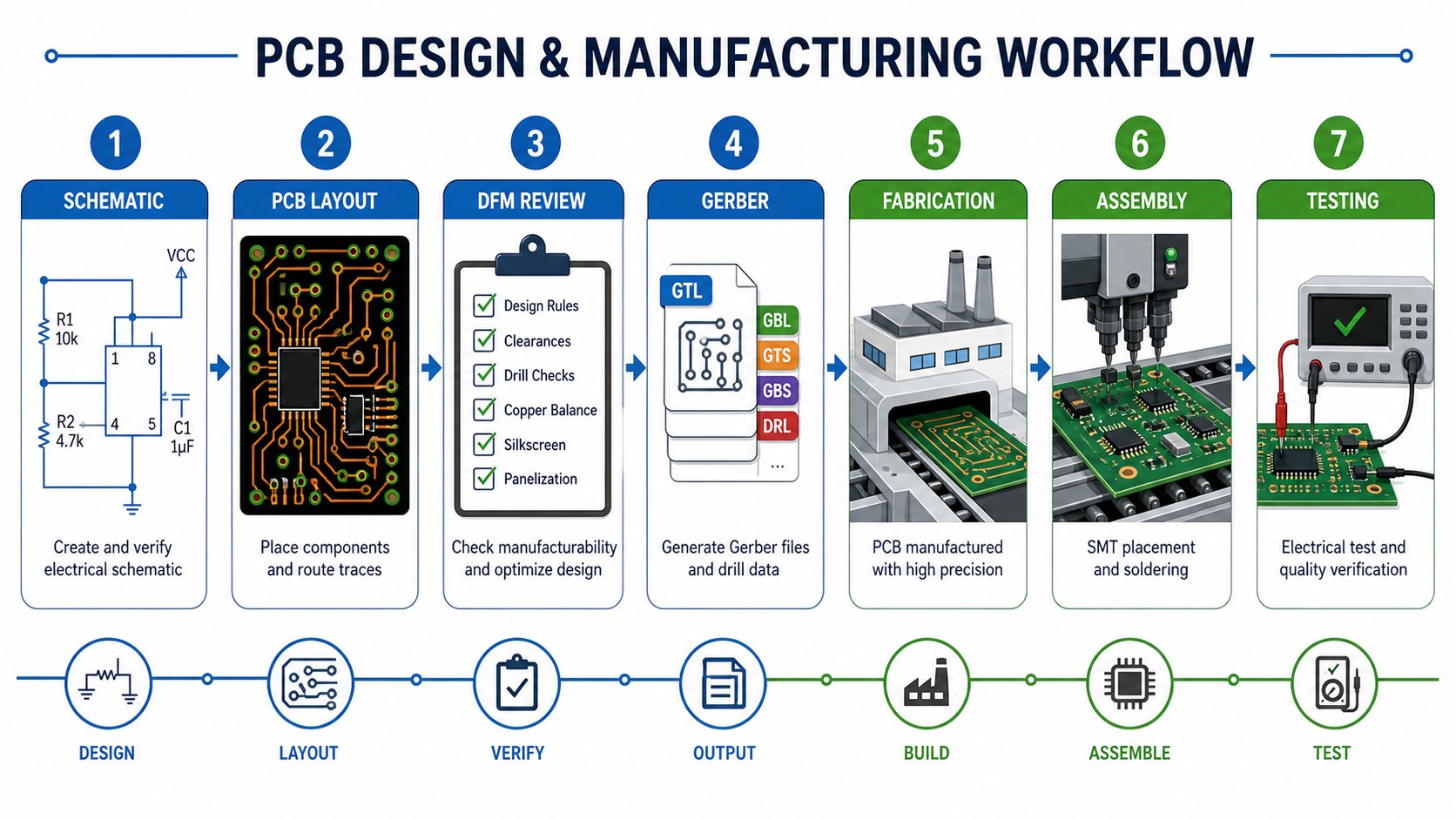
PCB manufacturing PCB manufacturing
Home > Blog

pcb design

PCB Design for Manufacturability Checklist Before Fabrication
Wednesday, July 15th, 2026

PCB design for manufacturability means checking a PCB layout against real fabrication and assembly constraints before the files are released for build. A useful DFM review catches file gaps, layout risks, material questions, assembly conflicts, and test problems early, when they are still easy to fix.

Use DFM before sending Gerber or ODB++ files for quotation, not after the first production problem appears. The goal is simple: help the board move from CAD data to PCB fabrication and PCBA with fewer engineering questions, fewer price changes, and fewer avoidable delays.

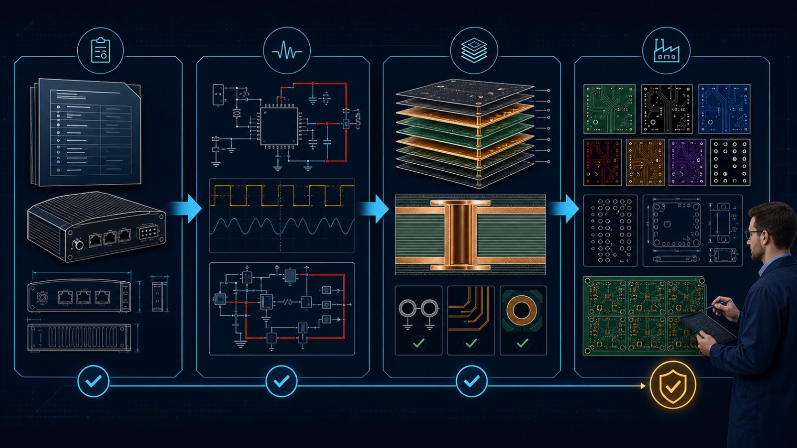
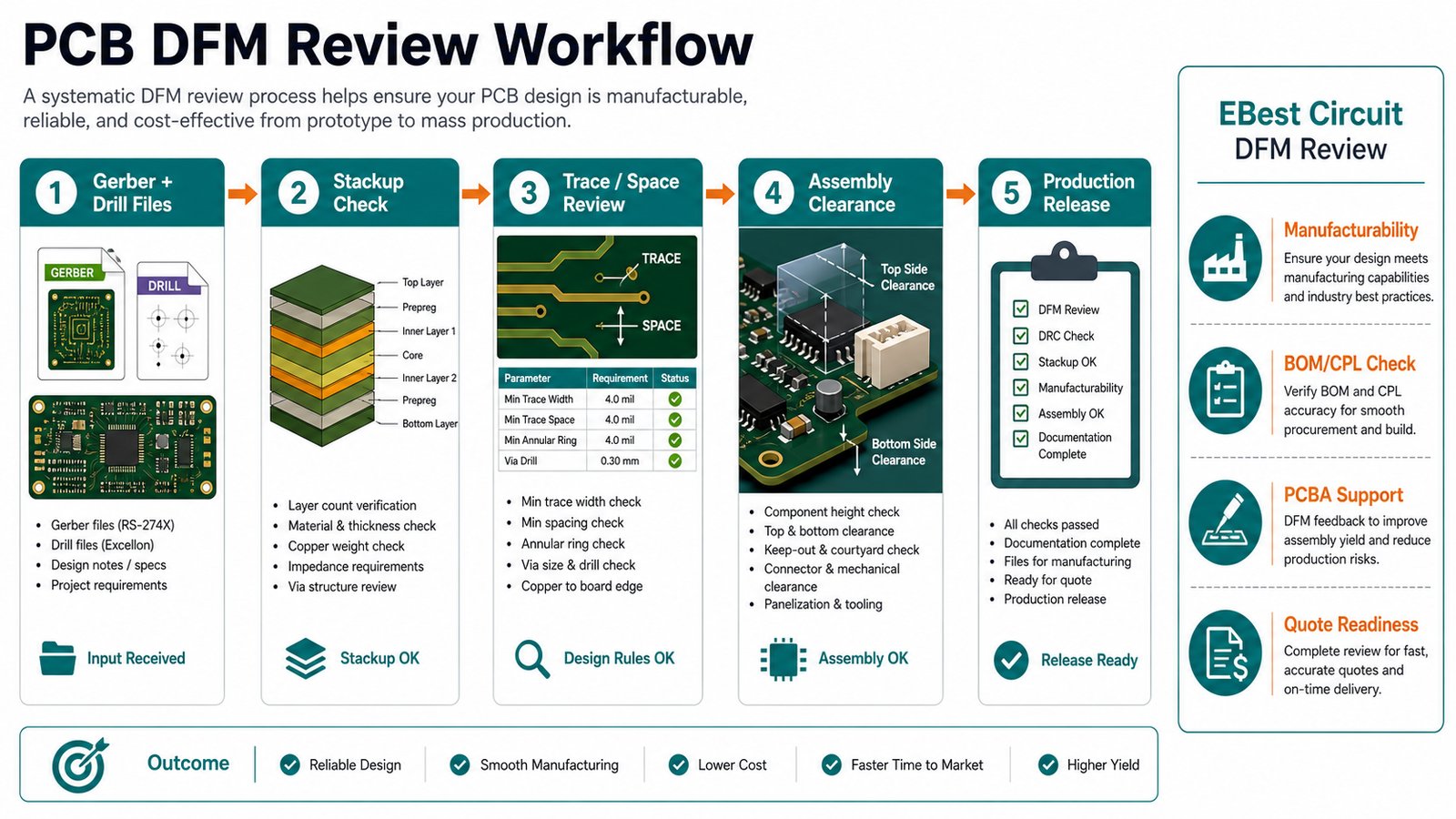
PCB design for manufacturability checklist with PCB layout Gerber review and inspection tools
PCB DFM works best when layout, stackup, drill, solder mask, assembly, and test details are reviewed before the files are released to manufacturing.

What PCB Design for Manufacturability Means

PCB design for manufacturability is the practice of designing a circuit board so it can be fabricated, assembled, inspected, and tested reliably by the chosen manufacturing process.

DFM is not only a software report. It is a practical engineering check between design intent and factory reality. The same schematic can be routed in a way that is easy to build or in a way that creates tight spacing, unclear drill data, soldering problems, poor test access, or repeated questions during quotation.

For buyers, DFM is a risk-control step. It helps decide whether the current file package is ready for a quote, prototype, pilot run, or production release. If the project also includes assembly, read DFM together with the PCB manufacturing and assembly guide so bare-board and PCBA risks are reviewed together.

When to Run a DFM Review

Run a DFM review before quotation, before prototype release, before production release, and whenever the board changes material, layer count, package density, or assembly method.

The best time is after layout is mature enough to export manufacturing data, but before purchase orders, panel plans, component commitments, or production schedules become fixed. At that point, the team can still adjust traces, vias, mask openings, component spacing, test pads, or drawings without turning every change into schedule pressure.

Project stage DFM focus Why it matters
Early prototype File completeness, obvious layout errors, package fit Prevents first-build rework and missing-file delays
Pilot build Repeatability, assembly access, test coverage Finds issues before the design is treated as stable
Production Yield risk, sourcing consistency, inspection method Reduces hidden cost and schedule surprises

Gerber, ODB++, Drill and Drawing Checks

The first DFM gate is file completeness, because unclear manufacturing data creates quote delays before anyone can evaluate the real board.

  • Confirm that all copper, solder mask, paste, silkscreen, outline, drill, and mechanical layers are exported.
  • Check whether the Gerber or ODB++ package matches the fabrication drawing and revision name.
  • Verify NC drill files, plated and non-plated holes, slots, cutouts, countersinks, and controlled-depth notes.
  • Remove old notes from previous revisions so the supplier does not quote against conflicting requirements.
  • Include a clear drawing when board outline, tolerances, impedance, panelization, or special processes matter.

If the same supplier will build and assemble the board, include BOM and CPL data early instead of sending bare-board files first and assembly files later.

Board Outline, Stackup and Material Checks

Board outline, stackup, thickness, material, copper, and impedance notes should be checked before release because they affect both manufacturability and quotation accuracy.

A design that looks correct in CAD may still create manufacturing questions if the outline is not closed, slots are not clearly defined, the stackup is missing, or the material is stated too loosely. For FR4, high Tg, RF, HDI, metal core, ceramic, flex, or rigid-flex work, the selected material route should be confirmed with the manufacturer instead of assumed from a generic rule.

For material-family context, BestPCBs product pages such as FR4 printed circuit boards and HDI PCB can be useful internal references, but exact limits should still be confirmed against the live project files.

Trace, Spacing, Via and Annular Ring Checks

Trace, spacing, via, drill, and annular ring rules should be checked against the intended process route, not copied from a generic internet table.

The safe rule is to design with margin. Very tight features may be possible on one process route and poor value on another. Before release, check whether the smallest trace, smallest gap, via type, drill-to-copper clearance, via-to-pad relationship, and board-edge clearance are appropriate for the supplier and the build quantity.

Item to check What can go wrong DFM action
Fine traces and spacing Yield loss, etching variation, re-quote Confirm rules before layout release
Small drills and vias Fabrication route changes or reliability questions Check drill table and annular ring margin
Vias near pads Solder wicking or assembly defects Review via-in-pad, tenting, filling, or spacing plan
Copper near board edge Routing damage or exposed copper Keep edge clearance consistent with the fabrication route

Copper, Solder Mask, Silkscreen and Surface Finish Checks

Copper weight, solder mask clearance, silkscreen placement, and surface finish should be checked together because they affect fabrication quality and assembly reliability.

DFM review should catch mask slivers, exposed copper, legend on pads, unclear polarity marks, and surface finish choices that do not match the assembly or storage requirement. The right finish depends on solderability, shelf life, pad design, component type, and project use, so it should be specified clearly in the RFQ instead of left as an assumption.

If cost is part of the decision, use the custom PCB cost guide together with the DFM checklist. Cost changes often come from the same details that make a design harder to build.

PCB Assembly DFM Checks

Assembly DFM checks whether the board can be populated, soldered, inspected, repaired, and tested without avoidable process risk.

For PCBA, bare-board manufacturability is only half of the review. Component footprint accuracy, part rotation, polarity marks, spacing around connectors, thermal relief, paste openings, BGA escape routing, tall-part clearance, and panel handling all matter. A board can pass fabrication review and still create assembly trouble.

  • Match BOM manufacturer part numbers to footprints and package data.
  • Check CPL or pick-and-place coordinates, rotation, side, and reference designators.
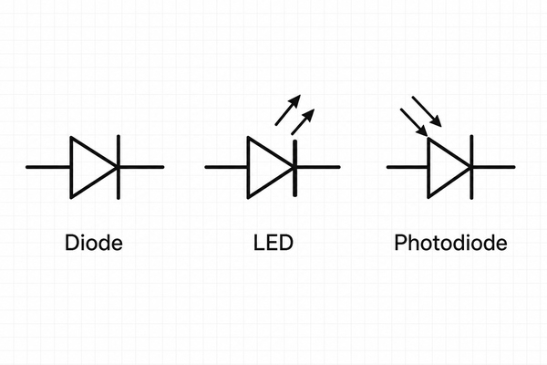
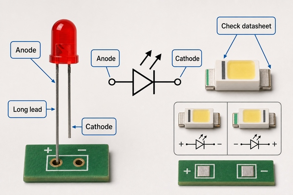
  • Make polarity, pin 1, connector direction, and LED orientation visible and unambiguous.
  • Review component spacing for soldering, inspection, rework, and enclosure fit.
  • Confirm whether special parts require hand soldering, selective soldering, fixtures, or extra inspection.

When the build includes assembly, the PCBA and PCB assembly service page is the natural service reference.

Test Point, Inspection and Quality Planning

DFM should include test and inspection planning because boards that cannot be inspected or tested efficiently carry higher production risk.

Ask how the board will be checked after fabrication and after assembly. Bare boards may need electrical testing. Assembled boards may need AOI, X-ray for hidden joints, functional test, fixture access, programming, or visual inspection. Test points should be accessible, labeled where needed, and compatible with the intended fixture or manual test method.

For capability context, the PCB test equipment page can support discussions about inspection and test expectations.

Cost and Lead-Time Risks Found by DFM

DFM often reduces cost and lead-time risk by finding manufacturability issues before they force a re-quote, redesign, material change, or assembly hold.

DFM issue Likely business impact How to reduce it
Missing drill or drawing data Quote delay Send complete manufacturing files first
Tight process features Higher cost or different route Confirm limits before final routing
BOM or CPL mismatch Assembly hold Review BOM, CPL, polarity, and footprint data together
Unclear testing need Late cost addition State electrical, AOI, X-ray, functional, or fixture needs early

DFM Checklist Before Releasing Files

A practical PCB DFM checklist should cover fabrication data, mechanical intent, assembly data, test requirements, and quotation scope before files are sent.

  • Gerber or ODB++ package includes every required layer and matches the revision.
  • NC drill, slots, plated/non-plated holes, cutouts, and board outline are clear.
  • Stackup, thickness, material, copper, impedance, finish, mask, and legend requirements are stated.
  • Smallest trace, spacing, drill, annular ring, and edge clearance are reasonable for the intended process route.
  • BOM, CPL, assembly drawing, polarity notes, approved substitutes, and special handling notes are complete.
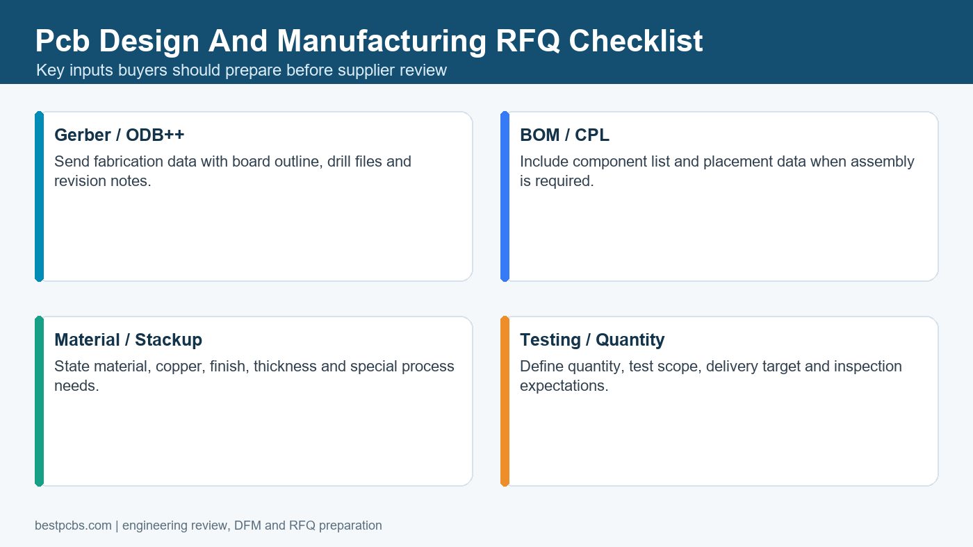
  • Test requirements, inspection expectations, delivery target, quantity, and packaging needs are stated.

What to Send for a PCB DFM Review

For a useful PCB DFM review, send the same package you expect the manufacturer to quote and build, not only a screenshot or incomplete Gerber export.

For bare PCB fabrication, send Gerber or ODB++, NC drill, fabrication drawing, stackup, material preference, copper, finish, tolerance notes, quantity, and target delivery. For assembly, add BOM, CPL, assembly drawing, polarity notes, component alternatives, programming needs, and test plan.

If component sourcing is included, make sourcing expectations explicit. The component sourcing service page is a useful reference when the DFM review also needs BOM availability and substitute approval.

How to Work With a PCB Manufacturer on DFM Feedback

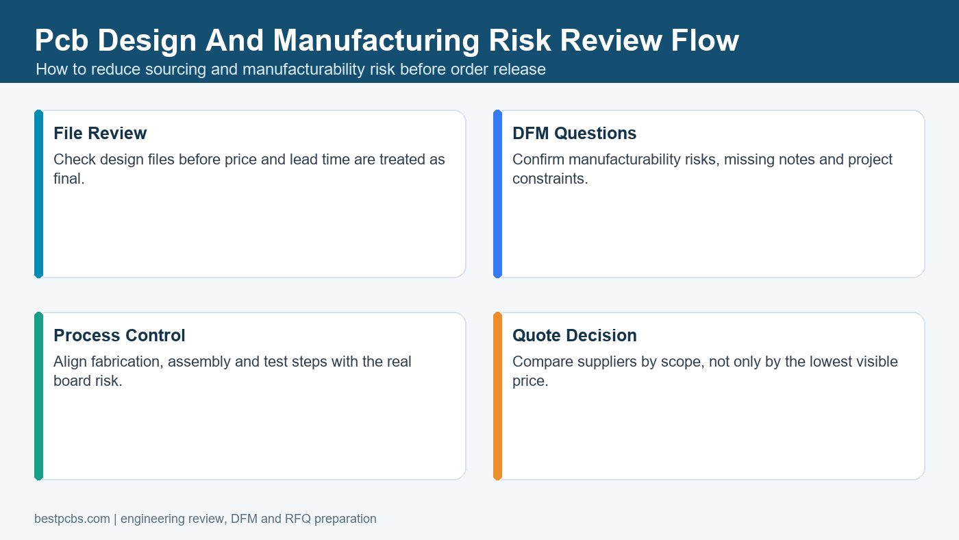
DFM feedback is most useful when the buyer and manufacturer agree which issues are mandatory fixes, which are recommendations, and which are acceptable project risks.

Do not treat every DFM comment as criticism of the design. Some comments protect yield, some clarify quotation scope, and some prevent assembly mistakes. Ask for the reason behind each major issue, then update the CAD source, exported files, fabrication drawing, BOM, or CPL so the approved change is visible in the next release package.

If your project is an early engineering build, the prototype PCB assembly page gives more context for prototype and small-batch review.

Common PCB DFM Mistakes

Common PCB DFM mistakes include incomplete files, unclear drawings, tight layout features without process confirmation, poor assembly markings, and missing test access.

Mistake Why it matters Better practice
Only Gerbers are sent for PCBA Assembly scope cannot be reviewed Send BOM, CPL, assembly drawing, and test notes
Old notes stay on drawings Supplier may quote the wrong requirement Clean revision notes before release
Polarity is unclear Assembly error risk increases Mark pin 1, diode, LED, capacitor, and connector orientation clearly
No test strategy is stated Late inspection or fixture cost may appear Define electrical, AOI, X-ray, or functional test needs early

Frequently Asked Questions About PCB Design for Manufacturability

What is PCB design for manufacturability?

PCB design for manufacturability is the process of checking a board layout, files, materials, assembly data, and test requirements against the way the board will actually be fabricated and assembled.

Is DFM only needed for complex PCBs?

No. Complex HDI, RF, flex, rigid-flex, or dense PCBA projects need deeper DFM, but even simple boards benefit from checking files, drill data, outline, polarity, and test requirements before quotation.

Can DFM reduce PCB cost?

DFM can reduce avoidable cost by finding problems that would otherwise cause re-quotes, fabrication questions, assembly holds, rework, or special process changes. It does not guarantee the lowest price; it helps make the quote more realistic.

What is the difference between DFM and DFA?

DFM focuses on whether the PCB can be manufactured reliably. DFA, or design for assembly, focuses on whether components can be mounted, soldered, inspected, and tested efficiently. PCBA projects need both.

Final Recommendation Before PCB Release
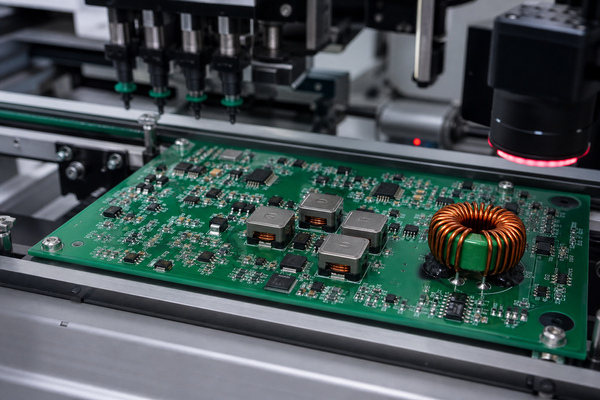
Before releasing a PCB for build, run one final DFM pass on the manufacturing files, assembly files, test requirements, and quotation assumptions.

If you want BestPCBs to review your design before fabrication or assembly, send Gerber or ODB++ files, NC drill files, stackup, fabrication drawing, BOM, CPL, quantity, material, surface finish, testing requirements, and target lead time through the contact page or email sales@bestpcbs.com. The clearer the file package is, the faster the team can confirm manufacturability, assembly scope, sourcing risks, and quotation details.

You may also like

Custom PCB Design for Teleoperation: Latency, Power and RF Checks
Monday, July 13th, 2026
Custom PCB design for teleoperation robot controller with remote control and lab test equipment

Custom PCB design for teleoperation should protect the remote-control link, motor-control power path, sensor feedback, test access and enclosure interface before the first prototype is ordered. A teleoperation PCB is not just a robot controller board. It carries the electronics that help an operator send commands, receive feedback and keep the machine predictable when wireless quality, vibration, load current or cable routing changes.

This guide is written for engineers and buyers preparing a custom PCB or PCBA for teleoperated robots, remote inspection equipment, mobile platforms, industrial manipulators, UAV ground systems, field-service devices or hazardous-area remote tools. It focuses on manufacturable PCB checks and RFQ readiness, not on robot-control algorithms.

What does custom PCB design for teleoperation need to control?

A teleoperation PCB needs to keep command input, feedback data, power conversion, motor drivers, sensors and safety-related I/O electrically separated enough to avoid unstable behavior. The design may include a microcontroller or processor, RF or wired communication module, camera or sensor inputs, encoder lines, motor-driver interfaces, battery or DC input, protection circuits and connectors to the robot body.

The board should be reviewed as a system. A clean schematic can still fail in the field if motor-current return paths disturb the receiver, if a camera interface sits beside a noisy regulator, or if a connector harness pulls against a weak solder joint. When wireless range, antenna routing or controlled impedance matters, compare the design against an RF PCB capability early instead of treating the radio section as a normal digital trace group.

Teleoperation PCB area Design check Why it matters
Communication link Antenna clearance, controlled routing, shielding, connector loss and RF module placement Weak links create command delay, dropouts or unstable feedback
Power input Battery/DC range, transient protection, regulator heat and local decoupling Remote machines often see load surges and cable voltage drop
Motor and actuator paths High-current loops, driver heat, return path and separation from sensors Motor noise can reset logic or corrupt feedback signals
Sensor feedback Encoder, camera, IMU, limit switch and telemetry routing The operator needs reliable state information, not only command output
Production test Programming access, test pads, fixture clearance and functional-test limits A prototype that cannot be tested repeatably is not ready for volume

How should latency and link reliability affect PCB layout?

PCB layout cannot remove all network delay, but it can reduce board-level causes of packet loss, noise coupling and unreliable command response. Teleoperation systems are sensitive to latency, jitter and communication dropouts, so the board should not add avoidable RF, grounding or power noise problems on top of the software and network layer.

Keep the antenna or RF module away from motor drivers, switching regulators, displays, dense cable bundles and metal enclosure walls unless the RF design intentionally accounts for them. Follow the module vendor’s keep-out and ground rules. If the design uses external antennas, review connector type, cable routing, mounting torque and enclosure feedthrough. If it uses wired control, check differential-pair routing, shielding, ESD protection and connector strain relief.

Teleoperation PCB signal validation with oscilloscope, RF cables and remote-control hardware
Teleoperation PCBs should be validated around command signals, feedback data and RF or wired communication paths.

Do not bury the communication decision inside a generic PCB order. If the board includes RF, Ethernet, CAN, RS-485, USB, camera links or high-speed sensor data, the stackup, reference planes and connector placement should be part of the RFQ review. Related control-network design checks are also covered in the custom PCB design for industrial networks guide.

What power architecture should a remote robot controller use?

The power architecture should separate noisy actuator energy from logic, RF, sensors and safety I/O while still sharing a controlled grounding strategy. Teleoperated equipment often combines battery packs, DC input, motor drivers, servos, radios, cameras, lamps, heaters or brakes. Those loads should not all be treated as a single quiet supply problem.

Start by listing each rail, load current, startup sequence, allowable voltage range and heat source. Use local decoupling for processors, RF modules and sensors. Keep high-current switching loops short. Give motor-driver current a planned return path instead of letting it travel under the communication and sensor sections. If the design has high-current power electronics, heavier copper, thermal vias, wider pours or separate power boards may be needed; do not infer current capacity from trace width alone without reviewing temperature rise and board stackup.

How should motor noise, sensors and safety I/O be isolated?

Motor-control noise should be handled with placement, return-path control, filtering, connector separation and test access before the PCB is released. Teleoperation failures are often blamed on software, but random resets, lost encoder counts, noisy video, false limit-switch signals and unstable IMU readings can come from board-level coupling.

Place motor drivers and power switching away from sensitive analog, RF and feedback circuits. Use clear zones for encoder inputs, current sensing, limit switches, emergency-stop inputs and feedback buses. Add test points for rails, reset lines, communication status, actuator enable lines and critical sensors. For first builds, treat the project as a Prototype PCB Assembly job so assembly feedback, component alternates and functional-test access can be corrected before production.

Which PCB materials and stackups fit teleoperation boards?

Most teleoperation controller boards can start with FR4, but RF, high-speed, thermal, vibration and enclosure constraints may require stackup changes. A simple two-layer board may work for low-speed prototypes. A production controller with RF, cameras, processors, motor drivers and many connectors usually benefits from four or more layers because planes improve return paths, noise control and routing density.

Use high-frequency laminates or hybrid stackups only when the RF section, bandwidth or antenna design justifies the cost. For compact mobile equipment, board outline, connector height, stiffeners and mounting holes can be as important as material choice. If a remote unit needs a folded sensor harness, moving camera module or tight enclosure path, review whether flex or rigid-flex is more reliable than multiple cable connectors.

What should be checked before PCBA production?

Before PCBA production, verify that the board can be assembled, programmed, calibrated, inspected and tested under realistic command and load conditions. A teleoperation controller should not rely only on visual inspection or continuity testing. It needs checks that match how the remote machine behaves.

Teleoperation controller PCBA inspection with connector harness test fixture and assembled control boards
Connector, harness and functional-test planning should be part of the teleoperation PCBA build package.

Define programming access, bootloader method, firmware version control, fixture pins, current-limit settings, communication checks and pass/fail criteria. Test the board with expected cable lengths, antenna placement and representative actuator loads when possible. Supplier-side PCB test equipment should be discussed before volume builds if the project needs fixture-based functional testing, not after the pilot run exposes missing pads.

How should connectors, harnesses and enclosures be planned?

Connectors and harnesses should be placed around assembly access, strain relief, service direction, cable noise and enclosure sealing. Teleoperated products often fail mechanically before they fail electrically: vibration loosens cables, operator ports get stressed, or enclosure walls block connector access.

Check connector locking style, mating cycles, wire gauge, cable bend radius, shield termination, gasket clearance and mounting screw access. Keep high-current motor wiring away from RF and sensor lines where possible. If the supplier is expected to deliver a tested controller inside a housing, discuss Box Build Assembly requirements such as harness routing, enclosure labels, final test and packing constraints.

RFQ checklist for custom teleoperation PCB design

A useful RFQ package should show the supplier the control architecture, RF or wired link, power budget, motor loads, enclosure constraints and test requirements. Without those details, the quote may cover board fabrication but miss the risks that make a teleoperation product hard to build.

  1. Gerber files, drill files, netlist, stackup, copper weight and controlled revision number.
  2. Schematic, BOM, approved alternates, centroid file and assembly drawing.
  3. Communication method: RF module, antenna type, Ethernet, CAN, RS-485, USB, camera link or mixed interfaces.
  4. Power input range, battery or DC supply notes, maximum load current and motor-driver information.
  5. Connector drawings, harness direction, enclosure model, mounting holes and height limits.
  6. Programming method, firmware loading requirement and board-level functional-test criteria.
  7. Environmental notes such as vibration, dust, humidity, outdoor use, heat, chemical exposure or service access.
  8. Any components that require sourcing approval, lifecycle review or controlled substitutes.

Teleoperation products often depend on RF modules, processors, connectors, motor drivers, sensors and power ICs that cannot be swapped casually. Involve Component Sourcing before the pilot build if approved alternates, lifecycle status or lead-time risk could change the control behavior.

Supplier questions buyers should ask

Supplier questions should force a real engineering review of link reliability, power integrity, assembly risk and test coverage. A low unit price is not useful if the first build cannot be programmed, calibrated or tested under load.

  • Which layout areas are most likely to affect RF range, command response or feedback quality?
  • Are the antenna, connector and enclosure positions compatible with the communication method?
  • Do motor-driver current paths stay away from logic, RF and sensor feedback?
  • Are all programming, debug and functional-test pads reachable after assembly?
  • Which parts need approved alternates before production?
  • Can the test fixture simulate command input, feedback output and representative load current?
  • What should change before moving from engineering prototype to pilot production?

FAQ

What is custom PCB design for teleoperation?

Custom PCB design for teleoperation means designing a circuit board for remote command input, machine feedback, communication, power conversion, motor control, sensors and production test. The board must support predictable remote operation, not only basic robot movement.

Does teleoperation always need an RF PCB?

No. Some systems use wired Ethernet, CAN, RS-485 or tethered control. RF PCB review becomes important when the board includes antennas, wireless modules, controlled-impedance traces, coax connectors or tight enclosure constraints that affect radio performance.

What causes unstable teleoperation controller behavior?

Common board-level causes include motor noise coupling into logic, weak power rails, poor grounding, antenna placement problems, cable shielding mistakes, missing ESD protection, inaccessible test pads and firmware loading issues. Network software can also matter, but the PCB should not add preventable electrical faults.

How many layers should a teleoperation controller PCB use?

Simple prototypes may use two layers, but four or more layers are often safer when the board has RF, processors, motor drivers, cameras, sensors and many connectors. Planes help control return paths, EMI, routing density and power integrity.

What files are needed for a teleoperation PCB quote?

Send Gerber and drill files, schematic, BOM, centroid file, assembly drawing, stackup, enclosure notes, communication method, power budget, connector drawings and test requirements. Include firmware-loading and functional-test notes if the supplier will assemble the PCBA.

Conclusion

Custom PCB design for teleoperation should be reviewed around the full control path: command link, RF or wired interface, power rails, motor noise, sensor feedback, connectors, enclosure and test access. A supplier can quote more accurately when the RFQ includes the board files plus communication, power, harness and functional-test requirements. For a remote-control product, that preparation is often the difference between a board that only powers up and a controller that can be built, tested and improved repeatably.

You may also like

Custom PCB Design for Sensors: Signal, Power and Test Checks
Monday, July 13th, 2026
Custom sensor PCB design workbench with sensor board, oscilloscope and enclosure parts

Custom PCB design for sensors should be reviewed around signal accuracy, low-noise power, grounding, connector placement, calibration access, test points, environmental protection and production-ready RFQ files. A sensor PCB is not only a small carrier board for a sensing element. It is the interface between the real world and the electronics that must read that signal consistently.

This guide is written for engineers and buyers preparing a custom sensor PCB or sensor PCBA for industrial devices, IoT products, environmental monitoring, equipment controls, medical-adjacent instruments, automotive modules or field equipment. It focuses on manufacturable board design and supplier review, not on selecting one specific sensor IC.

What does custom PCB design for sensors need to solve?

A sensor PCB needs to preserve the signal the sensor produces while surviving the mechanical, electrical and environmental conditions around the final product. The board may measure temperature, pressure, humidity, light, motion, gas, current, position or vibration, but the design checks follow a similar pattern: protect the signal path, control noise, provide stable power and make the board testable.

Low-current analog sensors may need guarded routing, short high-impedance traces and careful leakage control. Digital sensors may need clean I2C, SPI, UART, CAN, RS-485 or wireless module routing. Compact sensor products may use an HDI PCB when the enclosure is tight and the connector, MCU, RF section and sensing element compete for space.

Sensor board area PCB design check Buyer or engineer risk
Signal path Short routing, shielding, filtering, impedance or guard traces when needed Noise, drift or unstable readings can hide the real sensor output
Power supply Low-ripple rails, local decoupling, regulator heat and startup behavior Power noise can show up as false measurement changes
Grounding Analog/digital return paths, chassis connection and cable shield plan Ground loops or poor return paths can create hard-to-debug faults
Environment Coating, enclosure interface, sensor exposure window and connector sealing Humidity, dust, chemicals or vibration can change readings or damage the board
Production test Test pads, calibration points, programming access and fixture clearance Good prototypes can become slow or inconsistent in volume builds

Which sensor applications need a custom PCB?

A custom PCB is useful when the sensor board must fit a product enclosure, meet a specific noise target, connect to a harness, support calibration or survive a defined operating environment. Evaluation boards are useful for early testing, but they rarely match the size, connector, grounding, power and protection requirements of the final product.

Common examples include environmental sensor nodes, industrial monitoring modules, battery and charger sensors, flow meters, load-cell interfaces, motor feedback boards, optical sensor boards, wearable sensor modules and equipment health monitoring electronics. Many designs can use an FR4 Printed Circuit Board. High-frequency, wireless or antenna-connected sensor products may need RF material decisions, controlled routing or a review against an RF PCB capability page.

How should low-noise layout be planned?

Low-noise sensor layout starts with floorplanning: keep the sensor front end, reference, ADC, filter, connector and noisy switching circuits in controlled zones. A layout can pass a simple connectivity check but still produce unstable data if switching regulators, antennas, motors, relays or long cable inputs couple noise into the measurement path.

Custom sensor PCB DFM review with schematic, connector cables and layout notes
Sensor PCB design should be reviewed as a complete signal chain, not only as a component placement task.

Place the sensor and analog front end close together when the signal is small. Keep high-current switching loops away from sensitive inputs. Use a continuous reference plane where possible, and avoid splitting a return path under critical traces without a clear reason. For cable-connected sensors, review ESD, surge, filtering and shield termination before release. If the design uses a flex tail or adhesive-mounted sensing element, confirm bend area, stiffener position and assembly handling early.

What power and grounding checks matter most?

Power and grounding checks should answer whether the sensor reading stays stable during startup, load changes, communication bursts and nearby switching events. Sensors that look accurate on a bench supply can become noisy when they share power with radios, relays, motors, LEDs, heaters or long cable harnesses.

Ask the designer or supplier to review regulator choice, decoupling placement, reference voltage routing, ground return, cable shield strategy and any required isolation. If a sensor board includes both sensitive analog inputs and digital communication, the layout should support both signal integrity and production assembly. When the order includes SMT, through-hole parts, connectors and final inspection, discuss the project as a Prototype PCB Assembly or production PCBA job instead of a bare PCB only.

How should connectors, cables and enclosures be designed?

Sensor PCB reliability often depends on connector orientation, cable strain relief, enclosure clearance and how the sensor is exposed to the measured environment. A board can be electrically correct but hard to assemble if the cable exits the wrong side, the sensor window does not align, or the test pads are blocked by the housing.

Before fabrication, compare the PCB outline with the enclosure model, mounting bosses, gasket, sensor opening, cable routing and service access. For field devices, define whether the board needs conformal coating, potting, a vented enclosure, connector sealing or a separate daughterboard. If the supplier is expected to assemble the PCB into a housing or harness, treat the RFQ as a Box Build Assembly discussion.

When do flex or rigid-flex sensor boards make sense?

Flex and rigid-flex sensor boards make sense when the sensing element must sit away from the main electronics, bend around a shape, reduce connector count or fit a compact enclosure. They are common in wearables, medical-adjacent devices, compact industrial sensors, optical modules, probes and adhesive-mounted sensing assemblies.

Flex is not a shortcut around mechanical design. Bend radius, copper direction, stiffener location, adhesive choice, strain relief and assembly sequence still need review. If a sensor product uses a flexible circuit, compare the design against a proven custom flex PCB design checklist before ordering production tooling.

What should be included in the sensor PCB test plan?

The test plan should prove that the board can be fabricated, assembled, programmed, calibrated and checked repeatedly before it reaches the final product. For sensor PCBA, continuity alone is usually not enough. The test may need known input conditions, reference measurements, firmware loading, communication checks and pass/fail limits.

Sensor PCBA functional testing with oscilloscope, test fixture and environmental sensor enclosure
Plan functional test and calibration access before the board is released for production.

Add test pads for power rails, ground, programming, communication lines and critical analog nodes. Keep them reachable after assembly and enclosure installation. If calibration is needed, define the calibration input, equipment, firmware state and acceptable tolerance. A supplier’s PCB test equipment and fixture planning should be discussed before volume production, not after failed boards appear.

RFQ checklist for custom sensor PCB design

A strong RFQ package lets the supplier review sensor accuracy, manufacturability, assembly risk and test coverage before quoting price and lead time. Send controlled files instead of screenshots or partial exports.

  1. Gerber files, drill files, netlist and controlled revision number.
  2. Schematic, stackup, copper weight, board thickness and surface finish requirement.
  3. Sensor type, expected signal range, accuracy goal and calibration requirement.
  4. Power input range, current load, regulator notes and any battery or charger interface.
  5. Connector, cable, enclosure, coating, potting or gasket information.
  6. BOM, approved alternates, centroid file and assembly drawing for PCBA.
  7. Programming method, firmware loading requirement and functional test criteria.
  8. Environmental notes such as temperature, humidity, vibration, dust, chemicals or outdoor exposure.

Supplier questions buyers should ask

The best supplier questions force a real DFM and test review instead of a generic board price. Use them before approving the first build.

  • Which parts of this sensor design create the highest layout or assembly risk?
  • Are the sensor, connector and enclosure clearances consistent with the mechanical file?
  • Do any analog inputs need additional spacing, guarding, shielding or cleaning controls?
  • Are the test pads reachable after assembly and enclosure installation?
  • Which components have sourcing risk or need approved alternates?
  • Can the test fixture simulate or verify the sensor input reliably?
  • What should change before moving from prototype to pilot production?

Sensor boards often depend on stable parts. If a project uses specialized sensor ICs, connectors, filters, references or wireless modules, involve Component Sourcing early so substitutes do not change measurement behavior without engineering approval.

FAQ

What is custom PCB design for sensors?

Custom PCB design for sensors means designing a circuit board around a sensing element, signal chain, power system, connectors, firmware access and test plan for a specific product. The goal is to read the sensor accurately and build the board repeatedly, not just connect a sensor IC to a controller.

Does every sensor PCB need a four-layer board?

No. Simple low-speed digital sensor boards may work on two layers when routing, power and grounding are clean. Mixed-signal, wireless, compact or low-noise sensor boards often benefit from four or more layers because a stable reference plane and controlled return paths reduce layout risk.

What causes noise in sensor PCB readings?

Common causes include unstable power rails, poor grounding, long high-impedance traces, switching regulator noise, nearby motors or relays, cable pickup, weak shielding, poor filtering and bad test setup. The fix depends on the sensor type and signal level, so schematic and layout review should happen before fabrication.

What files are needed for a sensor PCB quote?

Send Gerber and drill files, schematic, stackup, board drawing, BOM, centroid file, assembly drawing, enclosure notes and test requirements. If calibration, coating, potting, firmware loading or box build is required, include those details in the first RFQ.

Can a PCB supplier improve sensor accuracy?

A PCB supplier can help with manufacturability, material choice, assembly quality, inspection and repeatable testing. Accuracy still depends on the sensor IC, circuit design, layout, calibration method, firmware and operating environment. Treat supplier feedback as one part of the engineering review.

Conclusion

Custom PCB design for sensors should start with the measurement problem, not with board price. Define the signal, power rails, grounding, enclosure, connector, calibration and test plan before production files are released. Then ask the supplier to review manufacturability and assembly risk against the real use case. That process gives the sensor board a better chance of producing stable readings in the final product.

You may also like

Custom PCB Design for Mining: Dust, Vibration and Power Checks
Monday, July 13th, 2026
Custom PCB design for mining equipment with rugged enclosure and connector harness

Custom PCB design for mining equipment should be reviewed around dust, moisture, vibration, protected power input, connector strain relief, thermal control, test points and production-ready RFQ files. A mining electronics board is not only a circuit layout. It is part of a rugged system that may sit near motors, pumps, sensors, conveyors, vehicles, lighting, chargers or communication devices where contamination, shock and repair access matter.

This guide is written for engineers and buyers preparing a custom PCB or PCBA for mining-related equipment. It focuses on practical design and manufacturing checks before fabrication or assembly. If the product will be used underground, near combustible dust, or in another regulated hazardous area, confirm the applicable equipment-level certification requirements with your compliance team. A PCB supplier can support design for reliability, traceability and production quality, but board fabrication alone does not certify the complete mining device.

What does custom PCB design for mining need to solve?

Mining PCB design needs to keep electrical performance stable while the board is exposed to dust, vibration, heat, moisture, long cable runs and maintenance stress. The exact risks depend on whether the board is used in a sensor node, motor controller, lighting module, communication gateway, battery system, display panel or test device.

For a simple monitoring module, the main issues may be enclosure fit, connector sealing and low-power reliability. For a power or drive-related board, the review moves toward copper weight, creepage and clearance, thermal paths and protection components. Compact control electronics may also need an HDI PCB if the enclosure is tight and the component density is high.

Mining design risk PCB or PCBA check Why it matters
Dust and moisture Enclosure interface, coating decision, connector sealing and cleaning process Contamination can create leakage paths, corrosion and intermittent faults
Vibration and shock Mounting holes, board support, connector retention and heavy component placement Loose connectors or cracked solder joints can stop equipment in the field
Power variation Input protection, grounding, copper width, fusing and transient protection Long cables and inductive loads can create voltage stress
Heat buildup Copper weight, thermal vias, enclosure contact and material selection Sealed boxes often have limited airflow
Maintenance Test points, labels in drawings, harness plan and replaceable modules Field teams need faults isolated quickly without damaging the board

Where are custom mining PCBs used?

Custom mining PCBs are common in control, sensing, communication, lighting, power conversion and equipment monitoring devices. A buyer should define the use case before asking for a quote, because a sensor interface board and a high-current control board need different materials, copper rules and test plans.

Typical examples include conveyor monitoring electronics, pump controllers, battery management devices, rugged displays, LED lighting modules, wireless gateways, environmental sensors and vehicle-mounted control units. Some designs use standard FR4 PCB construction. Others need heavier copper, higher Tg material, metal-backed structures, conformal coating, sealed box integration or full PCBA support.

How should dust, moisture and enclosure fit be handled?

The PCB should be designed together with the enclosure, gasket, connector system and cleaning/coating plan. Treating the board as a flat electrical drawing and the enclosure as a later mechanical decision often creates failures at cable entries, mounting bosses, edge clearance and service access.

Engineers reviewing a rugged mining equipment PCB with enclosure gasket and connector samples
Mining electronics should be reviewed as a board, enclosure, connector and testable assembly, not as a bare PCB only.

Before layout release, check the board outline against the enclosure drawing, connector keepout area, mounting-hole tolerance, coating keepout, service connector position and any pressure-equalization or sealing requirement. If conformal coating is planned, mark no-coat areas around connectors, switches, programming pads and test contacts. If potting is planned, confirm component height, thermal behavior and repair expectations before the production file is frozen.

What vibration checks matter before production?

Vibration risk is controlled by board support, connector retention, solder joint protection and heavy component placement. A mining PCB can pass an electrical review and still fail in the field if a large inductor, terminal block, relay, transformer, battery connector or harness load is not mechanically supported.

Use larger mounting margins around high-stress areas. Keep heavy parts away from unsupported board edges when possible. Add strain relief for harnesses instead of letting cable pull act directly on solder joints. For mixed SMT and through-hole designs, define whether wave soldering, selective soldering or hand operations are expected. If the design includes high-current terminals, compare the copper and spacing assumptions against a relevant design reference such as the Heavy Copper PCB Design Guide.

How should power input and heat be reviewed?

Power input review should cover voltage range, surge exposure, reverse polarity risk, grounding, heat flow and copper current capacity. Mining equipment often connects through long cables, battery systems, motors, relays, lighting modules or chargers. These conditions can put more stress on input circuits than a clean lab supply.

For early DFM, send the supplier the expected operating voltage, maximum current, copper weight, target temperature range, board thickness, surface finish and any thermal interface to the enclosure. Do not ask for only a bare board price if the real product needs heat-spreading, coated assembly, heavy connectors or functional testing. The quote should reflect the way the board will be used.

Design area Questions to answer before RFQ
Input power What voltage range, current load, fuse strategy and reverse-polarity protection are required?
Grounding How are chassis ground, signal ground and shield termination handled?
Thermal path Will heat leave through copper pours, vias, thermal pads, an enclosure wall or a heatsink?
Copper weight Are high-current traces sized for the real load and temperature rise target?
Protection Are surge, ESD and inductive switching risks reviewed at cable and connector interfaces?

Which materials and stackups fit mining electronics?

The material choice should follow the electrical load, enclosure temperature, vibration risk and required board density. FR4 is often suitable for control and sensor boards, but high-current, high-heat or compact assemblies may need different copper, laminate, via and thermal decisions.

For dense signal boards, HDI can reduce routing congestion and help fit a smaller rugged enclosure. For power boards, thicker copper, larger spacing and thermal planning may matter more than density. For LED lighting or heat-generating modules, metal-backed or direct thermal path designs may be considered. The right choice depends on the project files, not on a generic mining label.

How should assembly and sourcing be planned?

Mining PCBA planning should include component availability, substitute approval, coating or sealing steps, test fixture needs and final box-level handling. A bare PCB schedule does not describe the finished product if the order also needs SMT, through-hole assembly, wiring, enclosure fit or functional testing.

Before releasing the order, provide a controlled BOM, approved alternates, centroid file, assembly drawing, polarity notes, connector orientation, firmware loading requirement and test criteria. If long-life parts or industrial-grade components are required, discuss Component Sourcing early. If the supplier is expected to deliver a mounted board in a sealed housing, treat it as a Box Build Assembly discussion rather than a normal PCB-only purchase.

What test plan should be ready before release?

The test plan should prove the board can be built, inspected and checked consistently before it reaches the field. At minimum, define electrical test for bare boards, AOI or visual inspection for assembly, functional checks for powered boards and any project-specific connector, LED, sensor, relay or communication test.

Mining equipment PCB assembly under electrical test with rugged connector harness and sealed enclosure
Testing should be planned before production release, especially when cables, connectors, sealed boxes and field power inputs are involved.

Useful test points should be accessible after assembly, not hidden under large components or blocked by the enclosure. If the board has firmware, define how programming and verification are handled. If the product uses sensors, motors, relays or communication interfaces, list the pass/fail behavior in simple language. A supplier’s PCB test equipment capability should be part of the RFQ discussion when the board needs repeatable inspection instead of only continuity checks.

RFQ checklist for custom PCB design for mining

A useful RFQ package lets the supplier review reliability risks before quoting cost and lead time. Send the same controlled package to every supplier if you want to compare quotes fairly.

  1. Gerber files, drill files, netlist and controlled revision number.
  2. Board drawing with thickness, outline tolerance, mounting holes and connector keepouts.
  3. Stackup, copper weight, material preference and surface finish requirement.
  4. Expected operating voltage, current load, thermal concern and enclosure notes.
  5. BOM, approved substitutes, centroid file and assembly drawing if PCBA is included.
  6. Coating, potting, cleaning, labeling, packaging or box-build requirements.
  7. Test plan with required measurements, programming steps and pass/fail criteria.
  8. Compliance notes for the final equipment, especially if the use environment is regulated.

Supplier questions buyers should ask

The best supplier questions are specific enough to reveal whether the factory has reviewed the board as a mining electronics assembly, not just a generic PCB. Use the questions below before approving production.

  • Which part of this design creates the highest manufacturing risk?
  • Are the mounting holes, edge clearances and connector keepouts suitable for the enclosure?
  • Is the copper weight enough for the stated current and temperature target?
  • Do any components need adhesive, mechanical support or layout changes for vibration?
  • Which components have sourcing risk, and are substitutes already approved?
  • Can the test points still be reached after assembly or box build?
  • What should be changed before moving from prototype to production?

FAQ

What is custom PCB design for mining?

Custom PCB design for mining means designing a circuit board or PCBA for equipment used around mining operations, such as sensors, controllers, lighting, communication modules, power electronics or monitoring devices. The design must consider dust, vibration, moisture, power stress, enclosure fit, connectors, testing and production repeatability.

Does a mining PCB need a special material?

Not always. Many mining control or sensor boards can use FR4 when the electrical load and temperature are moderate. High-current, high-heat, compact or harsh-environment designs may need heavier copper, higher-grade laminate, HDI, metal-backed construction, coating or a different stackup. The material should follow the real design risk.

Can a PCB supplier certify mining equipment?

A PCB supplier can support reliable board fabrication, assembly, traceability, inspection and documentation. Certification for equipment used in regulated mining or hazardous environments is usually a system-level issue. Confirm ATEX, IECEx, MSHA or local requirements with qualified compliance specialists before production decisions.

What files are needed for a mining PCB quote?

Send Gerber files, drill files, board drawing, stackup, copper weight, surface finish, BOM, centroid file, assembly drawing, enclosure notes and test requirements. If the board will be coated, potted or installed in a sealed box, include those details in the first RFQ instead of adding them later.

What causes delays in mining PCB projects?

Common delays include unclear enclosure drawings, missing connector orientation, unapproved component substitutes, vague test criteria, incomplete power requirements and late coating or box-build decisions. A controlled RFQ package helps the supplier check manufacturability before committing to lead time.

Conclusion

Custom PCB design for mining should be treated as a rugged electronics project, not a normal board order with a different label. Start with the environment, enclosure, connectors, power input, heat path, component sourcing and test plan. Then ask the supplier to review the files for manufacturability before quote approval. That process gives the buyer a better chance of receiving a board that can be assembled, inspected and supported in real mining equipment.

You may also like

Custom PCB Design for Industrial Use: Enclosure, Power and I/O Checks
Monday, July 13th, 2026
Custom PCB design for industrial use with terminal blocks, power circuitry and test tools

Custom PCB design for industrial use means designing the bare board and assembly around the real installation: enclosure size, field wiring, power noise, vibration, temperature, moisture, service access and test coverage. A board that works on a lab bench can still fail in a cabinet, pump controller, sensor node or factory gateway if the PCB layout ignores connectors, grounding, protection, mounting and production test points.

For an industrial product, the best PCB design brief is not only a schematic and a Gerber file. It should explain the operating voltage range, load current, connector map, enclosure limits, ambient temperature, coating or potting needs, expected service life, and how the board will be tested before shipment. Those details help the PCB manufacturer catch risk before the design moves into fabrication and assembly.

What Is Custom PCB Design for Industrial Use?

Custom PCB design for industrial use is the process of turning an industrial product requirement into a manufacturable board layout that can survive field wiring, power variation, mechanical stress and repeatable production testing. It is different from a generic electronics board because the installation environment becomes part of the design input.

An industrial controller, power monitor or equipment interface often needs larger terminal blocks, screw mounting holes, isolation gaps, surge protection, clear service labels and room for hand tools. The base material may still be a standard FR4 Printed Circuit Board, but the layout rules, copper weight, coating decision and connector placement should be chosen for the real equipment, not for a clean prototype demo.

Start With the Enclosure, Not Only the Circuit

The enclosure fixes many PCB design decisions before trace routing begins. Board outline, mounting holes, connector direction, LED visibility, cable bend radius, airflow and service clearance all depend on the box or cabinet where the board will be installed.

Before layout, confirm the board outline against the mechanical drawing. Check whether connectors must face a panel opening, whether screw terminals need finger access, and whether high-voltage or high-current areas need physical separation from signal wiring. If the board is part of a complete product rather than a loose PCB, coordinate early with the Box Build Assembly plan so cable routing, labels, displays and mechanical fasteners are not solved after the PCB is already finished.

Enclosure factor PCB design check Why it matters
Mounting points Hole size, copper keep-out, washer clearance Prevents cracked solder joints and board flex
Panel connectors Connector height, orientation and access Avoids cable strain and rework during assembly
Airflow Heat source placement and component height Reduces hot spots in sealed or crowded cabinets
Coating or potting Keep-out around connectors, switches and test pads Prevents coating from blocking service points
Service access Readable silkscreen and reachable fuses/test points Helps technicians diagnose the unit in the field

Design the Power Input for Real Factory Conditions

Industrial PCB power design should assume voltage variation, switching noise, inrush current and wiring mistakes instead of assuming a perfect bench supply. The exact protection scheme depends on the product, but the layout should reserve room for protection, filtering and thermal relief.

For DC industrial boards, check reverse-polarity protection, fuse or resettable protection, surge or transient suppression, input filtering, regulator heat, copper width and connector current rating. For boards that switch motors, relays, heaters or solenoids, keep noisy current loops compact and separated from sensors, analog inputs and communication traces. High-current or high-heat industrial applications may need heavier copper, metal-core materials, ceramic substrates or another special PCB structure instead of a basic two-layer FR4 board.

Protect I/O Before It Reaches the MCU

Field I/O is one of the most common weak points in industrial PCB design because long cables carry noise, ESD, surge and wiring errors directly to the board edge. Treat every external connector as a risk entry point.

Place ESD or surge protection close to the connector when required. Keep isolation slots, creepage and clearance appropriate for the voltage category. Put pull-ups, filtering, common-mode chokes or termination near the interface they protect. For RS-485, CAN, Ethernet, sensor inputs or dry-contact I/O, make grounding and shield termination choices early so the PCB layout does not fight the installation wiring later.

Connector selection also affects assembly and sourcing. A design that depends on a rare terminal block or long-lead-time relay may be difficult to build during a shortage. Early Component Sourcing review helps confirm package availability, approved alternates and whether the BOM can support prototype and production builds.

Plan DFM, Assembly and Test Points Together

A good industrial PCB layout is not finished until assembly access and test coverage are planned. If test pads, programming headers and fixture access are added at the end, the board may pass a prototype build but become slow or expensive in production.

Confirm component orientation, panelization, fiducials, solder mask clearance, through-hole access, connector height and coating keep-outs before release. For the assembled product, define which rails, interfaces and functional outputs must be checked. The layout should include accessible test pads for ground, input voltage, main regulators, communication signals and critical sensor lines. A related engineering guide on Circuit Board Test Points can help teams decide which signals deserve fixture access before the first production batch.

If the supplier will handle both PCB fabrication and PCBA, PCB Assembly, SMT, PCB SMT by EBest Circuit (Best Technology), send the assembly drawing, BOM, pick-and-place file, test plan and coating requirements together. Separating fabrication questions from assembly questions often hides problems until parts are already on order.

Industrial PCB Design Checklist Before RFQ

The RFQ package should let the manufacturer review risk, not just quote a board size and layer count. Missing details usually turn into delayed questions, wrong assumptions or rework.

  • Gerber files, drill files, stackup notes and controlled impedance needs if applicable.
  • Board outline with enclosure drawing or DXF when connectors and mounting holes are critical.
  • BOM with manufacturer part numbers, approved alternates and lifecycle notes.
  • Assembly drawing with polarity marks, connector orientation and no-fit parts.
  • Expected environment: temperature, humidity, vibration, dust, splash, coating or potting.
  • Power input range, load current, surge concerns and isolation requirements.
  • Test requirements: programming, in-circuit checks, functional test and inspection points.
  • Packaging and box-build notes if the PCB ships as a complete module.

Common Mistakes That Make Industrial Boards Hard to Build

Most industrial PCB mistakes are not exotic layout errors; they are practical mismatches between the board, the cabinet, the wiring and the production process. Catching them before fabrication saves more time than debugging them after assembly.

Mistake Likely result Better design action
Connectors placed without cable clearance Field wiring bends sharply or blocks the cover Check cable path against enclosure CAD
No test access for power rails Production test becomes slow and manual Add test pads near regulators and protected I/O
Small copper paths for load current Heating, voltage drop or early failure Check copper width, copper weight and thermal relief
Protection parts far from connectors ESD or surge reaches sensitive ICs first Place protection near external entry points
No alternates for industrial connectors Build delay during component shortage Review BOM availability before final layout

Supplier Questions for an Industrial PCB Project

Use supplier questions to check whether the PCB manufacturer understands the product conditions, not only the drawing package. The answers should expose DFM gaps early.

  • Can you review connector clearance against the enclosure drawing?
  • Do any parts in the BOM have long lead time, EOL risk or weak alternates?
  • Which test points are needed for production fixture testing?
  • Should the board use thicker copper, different laminate, coating or selective keep-outs?
  • Can fabrication, assembly, coating and box build be reviewed as one workflow?
  • Which inspection records or test reports will be provided with the finished boards?

FAQ

What files are needed for a custom PCB design for industrial use?

Send Gerber and drill files, BOM, pick-and-place file, assembly drawing, board outline, enclosure drawing if available, test requirements and operating environment notes. For industrial boards, the enclosure, connector map, power range and coating requirements are often as important as the PCB data itself.

Does every industrial PCB need conformal coating?

No. Coating depends on moisture, dust, chemical exposure, voltage spacing and service requirements. If coating is needed, the PCB should include keep-outs around connectors, switches, jumpers, labels and test pads so coating does not block assembly or maintenance.

How should I choose materials for an industrial PCB?

Start with temperature, current, voltage, mechanical load and heat dissipation. FR4 is common for many control boards, but high-current, high-temperature, RF, heavy copper, metal-core or ceramic requirements may call for a different stackup or special PCB process.

Why do industrial PCBs need more test points than simple prototypes?

Production builds need repeatable checks. Test points give fixtures access to voltage rails, programming pins, communication lines and critical I/O. Without them, technicians may rely on slow manual probing or miss faults that only appear after installation.

Final Recommendation

For custom PCB design for industrial use, review the board as part of a field product: enclosure, wiring, power, I/O protection, assembly, sourcing and test coverage. The strongest RFQ package gives the manufacturer enough context to find DFM, BOM and reliability risks before the first boards are built.

You may also like

Custom PCB Design for Agriculture: Sensors, Power and Field Reliability
Monday, July 13th, 2026
Custom PCB design for agriculture with field sensor electronics and greenhouse equipment
Custom agriculture PCB projects need field-ready design choices before fabrication and assembly.

Custom PCB design for agriculture means designing a circuit board that can survive moisture, dust, vibration, unstable power, long cable runs, sensor drift and outdoor service conditions. A board used inside a soil sensor, irrigation controller, greenhouse monitor, livestock tracker or farm machine is not just a normal indoor PCB with a different enclosure.

The safest approach is to design the PCB, enclosure, connectors, power input, sensor interfaces, wireless layout and test plan together. If these decisions are left until production, the project may pass a bench test but fail after rain, washing, temperature cycling, fertilizer exposure or field vibration.

What Does Custom PCB Design for Agriculture Need to Solve?

Agriculture PCB design must solve environmental exposure and measurement reliability at the same time. The board may need to read weak sensor signals, run from battery or solar power, communicate wirelessly, drive pumps or valves, and keep working in wet, dusty and electrically noisy locations.

For a farm device, the PCB is often part of a larger field system. The same board may connect to soil probes, temperature sensors, humidity sensors, GPS modules, LoRa, NB-IoT, Bluetooth, motor drivers, solenoids or user controls. That mix creates real trade-offs: sensor accuracy needs clean analog layout, wireless modules need controlled antenna space, and outdoor wiring needs surge and reverse-polarity protection.

This is why the design review should start from the use case, not only from the schematic. A greenhouse data logger, a drip irrigation controller and a tractor-mounted control module can all be called agriculture electronics, but their PCB risks are different.

Application Main PCB design concern What to confirm before RFQ
Soil and moisture sensor node Low-noise sensing, waterproof cable entry, battery life Sensor type, probe connector, coating or potting limits
Irrigation controller Valve current, relay or MOSFET heat, surge protection Load current, cable length, transient protection and enclosure plan
Greenhouse monitor Humidity, condensation, wireless stability Operating temperature, antenna position and conformal coating area
Farm machine electronics Vibration, wide input voltage, connector strain Mounting method, power input range, harness and test standard
Livestock or asset tracker Battery life, RF performance, mechanical size Battery chemistry, sleep current target, antenna keep-out area

Which Field Conditions Change Agriculture PCB Design?

Moisture, dust, chemicals, temperature swing, vibration and unstable power are the conditions that most often change agriculture PCB design. If the board is specified like an office device, the first field failure may come from corrosion, connector leakage or a power transient rather than from the core circuit.

Humidity and condensation are common in greenhouses, irrigation cabinets and outdoor sensor boxes. If moisture can reach the PCB surface, high-impedance sensor circuits may drift and exposed copper may corrode. Designers should decide early whether the board needs conformal coating, selective coating keep-out zones, potting, sealed connectors or a vented enclosure.

Dust, mud and fertilizer residue can create another problem: they trap moisture and make cleaning difficult. Connector position, enclosure drain paths and service access matter. A connector that works in a lab may become a failure point if it faces upward, sits near a water path or lacks strain relief.

Power input also needs attention. Agricultural equipment may use long cable runs, solar charging, batteries, vehicle power or shared power rails. The PCB may need reverse-polarity protection, input filtering, surge suppression, brownout behavior and enough copper width for valve or motor loads. For material selection and base board planning, the FR4 printed circuit board page is a useful internal reference for common FR4 PCB options.

How Should Sensors, RF and Power Be Planned?

Sensors, RF and power should be planned as three interacting systems, not separate blocks. A low-power wireless agriculture board may fail if the antenna is blocked by the enclosure, if the sensor trace runs beside a switching node, or if the battery rail collapses during transmission.

Start with the sensor interface. Soil probes, pH probes, temperature sensors, flow meters and pressure sensors may use analog voltage, resistance, frequency, I2C, SPI, UART, RS-485 or other interfaces. Weak analog signals need short routing, guard spacing where needed, stable references and a quiet ground strategy. Digital sensors need connector mapping, ESD protection and firmware-accessible diagnostics.

Wireless planning should be handled before the mechanical layout is frozen. LoRa, Wi-Fi, Bluetooth, NB-IoT and cellular modules each need antenna clearance, ground reference, keep-out areas and sometimes matching components. If the enclosure is metal, wet or mounted near machinery, RF performance may change. The article on IoT sensor PCB assembly is a related page for sensor modules, wireless devices and PCBA test planning.

Power design should match how the device will really be used. A solar-powered field node may care most about sleep current and battery charging safety. An irrigation controller may care about surge protection and load current. A machine-mounted PCB may need wider input voltage tolerance, filtering and vibration-resistant connectors. Put current paths, heat sources and sensitive sensor traces in different layout zones when possible.

What Materials and Protection Choices Matter?

Material and protection choices matter because agriculture electronics often fail at the boundary between PCB, enclosure and environment. FR4 may be suitable for many projects, but the design still needs the right copper weight, solder mask coverage, surface finish, coating decision and mechanical support.

For many sensor boards and controllers, standard FR4 is a practical starting point. High Tg FR4, heavier copper, rigid-flex construction, aluminum PCB or ceramic PCB may be considered when temperature, current, bending, heat spreading or size constraints justify them. Do not choose a special material only because the application sounds harsh; choose it because the electrical, thermal or mechanical requirement makes it necessary.

Protection should be discussed with the manufacturer before assembly. Conformal coating can protect against moisture and residue, but it may interfere with connectors, test pads, switches, LEDs, sensor membranes or calibration points. Potting can improve sealing and vibration resistance, but it can make rework impossible and trap heat. A gasketed enclosure helps, but the PCB still needs proper connector orientation and creepage/clearance decisions.

Agriculture sensor PCB protection review with enclosure gasket, cable glands, coating sample and probes
Coating, enclosure sealing and connector choices should be reviewed before PCB fabrication and assembly.

If the device will face rain, spray, condensation or washing, compare the enclosure plan with PCB-level protection. The waterproof PCB guide explains coating, potting and protection trade-offs that are especially relevant to farm electronics.

How Should Connectors, Enclosures and Assembly Be Specified?

Connectors, enclosures and assembly should be specified before the PCB layout is released. In agriculture devices, many failures start at cable entry points, unsupported connectors, difficult assembly steps or missing test access.

Use locking or sealed connectors where field wiring is exposed to vibration, splash or repeated service. Place connectors so cables can be strain relieved and routed without sharp bends. If the device needs field replacement, the connector choice should match what a technician can handle with gloves, dust and limited visibility.

The enclosure affects PCB shape, mounting holes, connector height, antenna position, cable glands and service access. If the board needs a conformal coating process, mark coating keep-out areas in the drawing. If it needs potting, confirm component height, heat dissipation and whether any part must remain exposed to air.

Assembly files should not be treated as an afterthought. A clean BOM, centroid file, polarity notes, programming instructions, coating notes and test requirements reduce mistakes. For PCBA planning, the PCB assembly and SMT service page is the relevant service page to link when the article discusses prototype or production assembly.

What Testing Should Be Done Before Field Use?

Testing should prove that the PCB works electrically and that the field risks have been addressed. For agriculture electronics, a simple power-on test is not enough if the product will face moisture, vibration, long cables, battery sag or wireless range limits.

Start with normal manufacturing tests: visual inspection, AOI where applicable, continuity checks, programming, functional test and current consumption measurement. Add application-specific tests such as sensor calibration, wireless transmission, load switching, sleep current, input overvoltage behavior, reverse-polarity response and connector continuity after cable movement.

Environmental and mechanical validation depends on the project risk. A prototype may need humidity exposure, temperature cycling, splash simulation, vibration checks or enclosure sealing review. These tests should be defined with realistic limits rather than vague wording such as “outdoor grade.” If no formal standard is specified, record the actual test condition in the engineering notes.

Agriculture PCB field reliability testing with probes, battery input, connector harness and environmental chamber
Field reliability checks should include power input, connectors, sensor behavior and environmental exposure.

When writing the RFQ, include the required inspection method instead of assuming the supplier will infer it. The PCB test equipment page can support sections about inspection capability, while the custom PCB board fabrication guide is useful for file, stackup and process-check details before quotation.

Agriculture PCB Design Checklist for RFQ Files

A good RFQ package should let the PCB manufacturer understand the electrical design, field environment, assembly process and validation requirements. Missing environmental or test details often lead to a cheaper quote that does not match the real project risk.

  • Gerber or ODB++ files, drill files, board outline and stackup notes.
  • Schematic or design notes for sensor inputs, power input and communication interfaces.
  • BOM, centroid file, polarity notes and approved substitutes if assembly is required.
  • Material preference, copper weight, surface finish and solder mask requirements.
  • Enclosure drawing, mounting hole position, connector height and cable exit direction.
  • Coating, potting or no-clean requirements, including keep-out zones.
  • Operating temperature range, humidity exposure, splash/dust exposure and vibration concern.
  • Programming, calibration, current consumption and functional test requirements.
  • Prototype quantity, pilot quantity, mass production estimate and expected revision plan.
  • Any standards, customer test methods or acceptance criteria that must be followed.

If the agriculture device uses long cables, wireless modules, battery power or outdoor enclosures, send mechanical and use-case information early. The PCB supplier can review DFM, panelization, assembly handling and test access only if those details are visible before fabrication.

FAQ About Custom PCB Design for Agriculture

What is custom PCB design for agriculture?

Custom PCB design for agriculture is the process of designing a circuit board for farm, greenhouse, irrigation, livestock, sensor or machinery electronics. It must consider the circuit function and the field environment together, including moisture, dust, vibration, power input, connectors, sensor accuracy and testing.

Can a normal PCB be used in agricultural electronics?

A normal FR4 PCB can be used in many agriculture devices, but only if the design also handles enclosure sealing, connector protection, coating or potting needs, power input risk and test access. The problem is usually not the word “FR4”; it is whether the board was designed for field exposure.

What sensors are common in agriculture PCB projects?

Common sensors include soil moisture, temperature, humidity, light, pH, pressure, flow, GPS, accelerometers and gas sensors. The PCB layout should match the sensor interface. Analog sensors need noise control, while digital and wireless sensor modules need connector, ESD and firmware test planning.

Does an agriculture PCB need conformal coating?

It depends on the exposure level. Coating is useful for humidity, condensation and light contamination, but it should not cover connectors, switches, some sensors, programming pads or calibration areas. Decide coating zones before assembly, not after the finished PCB already has access problems.

What power problems affect agriculture electronics?

Battery sag, solar charging variation, long cable voltage drop, reverse polarity, pump or valve transients and vehicle power spikes can all affect agriculture PCBs. The design may need input filtering, TVS protection, fusing, reverse-polarity protection, brownout handling and enough copper width for load current.

How should wireless modules be placed on farm device PCBs?

Wireless modules should be placed with the antenna keep-out area, enclosure material, ground reference and cable locations in mind. A module that works on a bench may lose range inside a metal box, near wet soil, beside a battery pack or under a poorly positioned cable harness.

What files should I send for an agriculture PCB quote?

Send Gerber or ODB++ files, drill data, board outline, stackup, BOM, centroid file, enclosure drawing, connector information, coating or potting notes, environmental conditions, test requirements and expected quantities. If the project includes firmware loading or calibration, include those instructions too.

Is potting better than conformal coating for farm electronics?

Potting can provide stronger sealing and vibration support, but it can trap heat and prevent rework. Conformal coating is lighter and easier to inspect, but it does not seal the whole product. The right choice depends on moisture exposure, service needs, heat and mechanical stress.

How can buyers reduce prototype risk?

Build the first prototype with test points, connector access, programming access and clear environmental notes. Test power input, sensor reading, wireless range, current consumption and enclosure sealing before mass production. Do not wait for a large batch to discover that a connector, antenna or coating zone is wrong.

Should agriculture PCB design be handled before or after enclosure design?

It should be handled together with enclosure design. Board outline, antenna location, connector direction, gasket pressure, cable strain relief, coating keep-outs and service access all depend on the enclosure. Treating the enclosure as a late packaging step often creates avoidable redesign.

Final Supplier Notes for Agriculture PCB Projects

Agriculture electronics are usually judged in the field, not only at the lab bench. A good custom PCB design for agriculture should make the sensor readings stable, the wireless link practical, the power input protected, the connectors serviceable and the production test clear.

Before ordering, review the field environment, enclosure, cable harness, coating plan, power input and test requirements with the PCB supplier. If you are sourcing custom PCB design, PCB fabrication or PCB assembly for agriculture sensors, irrigation controllers, greenhouse devices or farm equipment, send your files and field requirements to our engineering team for DFM review and quotation at {contact_email}.

You may also like

Copper Pad PCB Design Guide: From DFM to Reliable PCBA
Monday, June 1st, 2026

Copper pad design plays a direct role in PCB solderability, current flow, mechanical bonding, test access, and long-term circuit reliability. On a circuit board, these exposed copper areas may look simple, but they carry several important functions. They connect components, support solder joints, provide test points, and help create stable electrical interfaces.

This guide explains what a copper pad is, how it differs from a solder pad or copper contact pad, how pads are made during PCB fabrication, what surface finishes are used, and how damaged pads can be handled during prototyping or board evaluation.

If your project involves fine-pitch components, high-current pads, contact pads, or repeated soldering concerns, an early DFM review can help identify risks before fabrication and assembly. Best Technology provides PCB manufacturing, PCBA assembly, surface finish guidance, and engineering support for prototype and production projects. For a technical review or quotation, pls feel free to send your Gerber files and BOM to sales@bestpcbs.com.

Copper Pad

What Is a Copper Pad on a PCB?

A copper pad on a PCB is a defined copper area used for electrical connection, component attachment, testing, or signal transfer. It is created from the copper layer of the circuit board and exposed through the solder mask so that solder, probes, connectors, or conductive surfaces can make contact with it.

In PCB manufacturing, copper pads are formed together with copper traces, planes, vias, and other conductive features. During fabrication, unwanted copper is removed through imaging and etching, leaving the designed circuit pattern on the board. After that, solder mask is applied, and selected pad areas remain open for assembly or contact.

A PCB may contain many types of pads, including:

  • SMT pads for surface mount components
  • Through-hole pads for leaded components
  • Via pads for interlayer connection
  • Test pads for ICT or functional testing
  • Connector pads for board-to-board or cable interfaces
  • Thermal pads for heat transfer under power components
  • Edge contact pads for card-edge connectors
Copper Pad

Each pad type has its own design requirements. An 0402 resistor pad, for example, is very different from a high-current terminal pad or a BGA pad. The layout engineer must consider component footprint, assembly process, current capacity, plating finish, and inspection method before finalizing the pad design.

Copper Pad

What Is the Difference Between a Copper Pad, Solder Pad, and Copper Contact Pad?

These terms are sometimes used interchangeably, but they are not exactly the same. Understanding the difference helps engineers communicate clearly with PCB manufacturers and assembly teams.

TermMeaningCommon Use
Copper padA copper area designed on the PCB layoutGeneral term for exposed or plated copper features
Solder padA pad designed to receive solder and attach a componentSMT and through-hole component assembly
Copper contact padA conductive contact area for mechanical or electrical contactConnectors, switches, test probes, battery contacts
Test padA pad used for electrical testingICT, flying probe, functional test
Thermal padA pad used for heat transfer and sometimes groundingPower ICs, LEDs, MOSFETs, thermal vias

A solder pad is usually a copper pad with a surface finish applied, such as ENIG, HASL, OSP, immersion silver, or immersion tin. Its main purpose is to form a reliable solder joint between the PCB and the component terminal.

A copper contact pad may not always be intended for soldering. It may be used for spring contacts, pogo pins, keypads, battery terminals, or edge connectors. In these applications, wear resistance, flatness, plating hardness, and oxidation control become very important.

For example, a gold-plated edge connector pad is a copper contact pad. It needs strong abrasion resistance because it may be inserted and removed many times. A standard SMT capacitor pad has a different requirement: it needs good solder wetting and accurate solder paste deposition.

Copper Pad

What Does a Copper Pad Do in PCB Assembly?

During PCB assembly, pads provide the interface between the bare circuit board and electronic components. The solder paste is printed onto the pads, components are placed on top, and the assembly is heated during reflow soldering. When solder melts and wets the pad surface, it creates both mechanical attachment and electrical continuity.

A properly designed pad supports several assembly goals.

It helps solder wet evenly.

  • Good solder wetting depends on a clean surface, suitable finish, correct pad geometry, and proper reflow profile. When these factors are controlled, solder spreads across the pad and forms a stable joint.

It keeps components in position.

  • Pad symmetry matters. If one pad is much larger than the other, or if thermal connection is uneven, small components may shift during reflow. This can lead to tombstoning, skewing, or weak solder joints.

It supports electrical performance.

  • The pad connects the component terminal to traces, vias, planes, or other copper features. For high-speed, RF, or high-current boards, pad geometry can affect impedance, parasitic capacitance, current distribution, and heat spreading.

It improves inspection access.

  • Pads must allow AOI, X-ray, probe testing, or visual inspection depending on the board type. For BGA packages, hidden solder joints may require X-ray inspection. For test points, pad size and spacing must match fixture or flying probe capability.

It contributes to mechanical reliability.

  • A pad must stay bonded to the PCB substrate through soldering, handling, thermal cycling, and product operation. Copper adhesion, laminate quality, surface treatment, and assembly temperature all influence pad strength.

In short, pad design connects PCB fabrication with PCBA reliability. A small layout decision can affect paste printing, placement accuracy, solder joint quality, test coverage, and field performance.

Copper Pad PCB Design: Size, Shape, Clearance, and Annular Ring

A strong PCB pad design starts with the component datasheet and IPC footprint guidance. The pad must match the component lead, terminal, or ball while also fitting the assembly process used by the manufacturer.

Pad Size
Pad size affects solder volume, wetting area, and joint strength. If the pad is too small, solder coverage may be insufficient. If it is too large, solder may spread too far and create floating, skewing, or bridging risks. For fine-pitch ICs, even a slight size deviation can affect assembly yield.

For SMT components, pad size is usually determined by:

  • Component terminal dimensions
  • Solder fillet requirement
  • Placement tolerance
  • Solder paste stencil design
  • Assembly process capability
  • Product reliability class

Pad Shape
Common pad shapes include rectangular, round, oval, square, and custom thermal shapes. Rectangular pads are common for chip resistors, capacitors, IC leads, and connectors. Round or oval pads are often used for through-hole parts and vias.

For RF or high-frequency boards, pad shape may also influence signal transition. In these cases, pad design should be reviewed together with impedance control, reference plane continuity, and via structure.

Clearance
Clearance is the spacing between a pad and nearby copper features. It affects manufacturability, voltage isolation, solder mask definition, and assembly quality. High-voltage circuits need larger clearance and creepage distance. Fine-pitch designs require tighter control from the PCB manufacturer.

Designers should check clearance between:

  • Pad to pad
  • Pad to trace
  • Pad to via
  • Pad to copper pour
  • Pad to board edge
  • Pad to mechanical hole

Annular Ring
For plated through-hole pads and vias, the annular ring is the copper area surrounding the drilled hole. It provides a reliable connection between the plated barrel and the surface copper pad.

If the annular ring is too narrow, drilling tolerance may reduce copper support around the hole. This can affect soldering, mechanical strength, and electrical connection. For high-reliability boards, annular ring design should consider drill accuracy, finished hole size, copper plating thickness, and IPC class requirements.

Solder Mask Opening
Solder mask defines which part of the copper surface is exposed. Two common pad styles are solder mask defined and non-solder mask defined.

Pad StyleDescriptionTypical Use
Non-solder mask definedSolder mask opening is larger than the copper padCommon SMT pads
Solder mask definedSolder mask overlaps the copper pad edgeSome BGA and fine-pitch applications

Non-solder mask defined pads are widely used because the copper edge defines the solderable area. Solder mask defined pads can help control pad exposure in certain dense designs, but they require precise solder mask registration.

How Are Copper Pads Cut, Etched, and Plated on a PCB?

Copper pads are not usually “cut” one by one. They are formed during the PCB imaging and etching process. The manufacturer starts with copper-clad laminate or copper foil laminated onto the PCB core. The desired circuit pattern is transferred onto the copper surface using photoresist and imaging.

The general process includes:

  • Copper-clad material preparation
    The PCB base material is prepared with copper foil on one or both sides, depending on the stack-up.
  • Cleaning and surface preparation
    The copper surface is cleaned to improve photoresist adhesion and imaging accuracy.
  • Photoresist application
    A photosensitive film is applied to the copper surface.
  • Circuit imaging
    The pad, trace, and plane pattern is exposed using the PCB artwork data.
  • Developing
    Unwanted photoresist is removed, leaving protected copper areas according to the circuit design.
  • Etching
    Exposed copper is chemically removed. The remaining copper forms pads, traces, and other conductive features.
  • Drilling and plating
    For plated holes and vias, drilling is followed by copper deposition and electroplating to create conductive barrels.
  • Solder mask application
    Solder mask covers most copper areas while leaving pads exposed.
  • Surface finish
    A protective finish is applied to exposed pads to improve solderability and prevent oxidation.

For multilayer PCBs, copper pads may exist on outer layers, inner layers, or both. Inner-layer pads connect to vias or buried structures, while outer-layer pads are often used for assembly and testing.

Etching accuracy matters because copper width, pad size, and spacing must remain within manufacturing tolerance. The final pad geometry depends on copper thickness, etching compensation, imaging accuracy, and process control.

What Surface Finishes Are Used on Copper Pads?

Bare copper oxidizes when exposed to air. Oxidation can reduce solderability and create unreliable contact surfaces. For this reason, exposed pads are protected with a surface finish after solder mask processing.

The surface finish should match the assembly method, component type, shelf-life requirement, cost target, and reliability expectation.

Surface FinishMain FeaturesCommon Applications
HASLGood solderability, cost-effective, uneven surfaceGeneral electronics, larger components
Lead-Free HASLRoHS-compatible version of HASLStandard lead-free assembly
ENIGFlat surface, good solderability, nickel-gold structureFine-pitch ICs, BGA, high-reliability PCB
OSPOrganic coating, flat and economicalSMT boards with controlled storage and fast assembly
Immersion SilverFlat finish, good conductivityHigh-speed, RF, and lead-free assembly
Immersion TinFlat surface, good solderabilityPress-fit, fine-pitch, and selected lead-free applications
Hard GoldExcellent wear resistanceEdge connectors, keypads, contact pads
  • ENIG is widely used for fine-pitch components because it provides a flat soldering surface. The nickel layer acts as a diffusion barrier, and the thin gold layer protects the nickel before soldering.
  • OSP is common for cost-sensitive SMT production. It protects copper pads before assembly but requires good storage control and proper handling.
  • Hard gold is preferred for copper contact pad applications where repeated mechanical contact is expected. It is not the same as soft immersion gold used in ENIG. Hard gold is thicker and more wear-resistant.
  • HASL provides strong solderability but may create an uneven surface. For very fine-pitch components, BGA, or small passive components, flatter finishes are usually preferred.

Choosing the right finish helps improve solder joint consistency, test contact stability, and long-term product reliability.

How to Fix a Copper Pad on a Circuit Board?

A lifted or missing pad can happen during prototype debugging, excessive rework, overheating, mechanical stress, or poor handling. In lab repair, technicians may use micro-jumpers, conductive epoxy, replacement pad kits, or copper foil methods to restore electrical connection. However, for production boards, pad damage should be treated as a process or design issue, not a normal repair step.

Common causes of pad damage include:

  • Excessive soldering iron temperature
  • Long dwell time during manual rework
  • Poor copper adhesion to the laminate
  • Repeated component removal
  • Strong mechanical pulling force
  • Incorrect footprint design
  • Insufficient annular ring on through-hole pads
  • Incompatible reflow or rework profile

For prototypes, a technician may repair a damaged pad by reconnecting the component terminal to the correct trace or via. If the original pad is connected to a nearby trace, a fine wire jumper may be used. If it connects to a via or inner layer, the repair becomes more difficult and requires careful electrical verification.

Copper tape is sometimes used as a temporary repair material. It may help recreate a missing solderable area in low-risk prototypes, but it is not a preferred solution for production electronics. Adhesion strength, solderability, current capacity, and long-term stability must be checked carefully.

For manufacturing improvement, the better approach is to review:

  • Pad size and copper area
  • Laminate selection
  • Copper peel strength
  • Soldering temperature profile
  • Rework method
  • Component footprint
  • Operator handling process
  • Board storage and moisture control

If pad lifting appears repeatedly, the board design and assembly process should be reviewed together. A DFM check can identify pad geometry issues, thermal imbalance, solder mask problems, and potential assembly risks before mass production.

For PCB projects requiring stable pad quality, Best Technology can support PCB fabrication, surface finish selection, DFM review, PCBA assembly, and testing. For project discussion or quotation, contact sales@bestpcbs.com.

FAQs About Copper Pad

1. What is a copper pad on a PCB?
A copper pad is a defined copper area on a circuit board used for soldering, electrical contact, testing, or connection. It can support SMT components, through-hole leads, probes, connectors, or thermal transfer structures.

2. Is a copper pad the same as a solder pad?
Not always. A solder pad is a type of copper pad designed for soldering components. A copper pad can also be used as a contact pad, test pad, via pad, or thermal pad.

3. What is a copper contact pad used for?
A copper contact pad is used for direct electrical contact. Common examples include edge connectors, spring contacts, pogo pin test points, keypad contacts, and battery terminals. These pads often need a durable surface finish such as hard gold.

4. How are copper pads made on a PCB?
Copper pads are formed through PCB imaging and etching. The manufacturer protects the required copper pattern and removes unwanted copper. After solder mask processing, exposed pads receive a surface finish such as ENIG, HASL, OSP, immersion silver, or hard gold.

5. Why do copper pads need surface finish?
Bare copper can oxidize. A surface finish protects the pad, improves solderability, and supports reliable electrical contact. The finish is selected based on assembly process, component pitch, storage condition, and product reliability requirements.

6. Can you replace a missing solder pad with copper tape?
Copper tape may be used as a temporary prototype repair in some simple cases. It should be verified for adhesion, electrical continuity, solderability, and current capacity. For production boards, redesign, controlled rework, or professional process review is a better solution.

7. Why does a copper pad lift from a PCB?
Pad lifting can be caused by excessive heat, repeated rework, mechanical force, weak copper adhesion, poor footprint design, or unsuitable soldering conditions. Reviewing the pad design and assembly profile helps prevent repeated failures.

8. Which surface finish is best for copper pads?
There is no single best finish for every PCB. ENIG is suitable for fine-pitch and BGA assembly, OSP is economical for controlled SMT production, HASL works well for many general boards, and hard gold is suitable for contact pads that require wear resistance.

Have a PCB or PCBA project that requires reliable copper pad design? Best Technology supports rigid PCB, multilayer PCB, HDI PCB, flexible PCB, rigid-flex PCB, heavy copper PCB, aluminum PCB, copper substrate PCB, ceramic PCB, and Rogers/high-frequency PCB manufacturing, together with DFM review, surface finish guidance, component sourcing, PCBA assembly, and testing.

If you would like our engineering team to help review pad size, solder mask opening, annular ring, copper thickness, surface finish, or soldering reliability before production, please feel free to send your Gerber files and BOM to sales@bestpcbs.com. We would be glad to provide a technical review or quotation based on your project needs.

You may also like

Aluminum PCB Circuit Board Complete Guide
Thursday, May 14th, 2026

What Is an Aluminum PCB?

An aluminum PCB is a printed circuit board with an aluminum metal base. It is also called an aluminum core PCB, metal core PCB, or MCPCB. Its main purpose is to move heat away from components.

aluminum pcb circuit board

A normal FR4 PCB uses fiberglass as the base material. However, an aluminum PCB uses a metal base. Because aluminum transfers heat better than FR4, It helps reduce heat accumulation around high-temperature components.

Typical aluminum-based printed circuit board has three main layers,as following:

LayerMain JobWhy It Matters
Copper Circuit LayerCarries current and signalsHelps the circuit work
Thermal Dielectric LayerMoves heat and insulates electricityControls heat and safety
Aluminum Base LayerSpreads heatKeeps the board cooler

The copper layer forms the circuit. The dielectric layer moves heat downward. Then, the aluminum base spreads the heat into the housing, air, or heat sink.

Because of this structure, aluminum PCB is a strong choice for LED lights, power boards, and other heat-sensitive products.

How Does an Aluminum PCB Circuit Board Dissipate Heat?

An aluminum PCB circuit board dissipates heat through a short heat path. First, heat starts at the component. Then, it moves into the solder joint and copper layer. After that, it passes through the dielectric layer. Finally, it reaches the aluminum base.

The heat path is usually:

Component → Solder Joint → Copper Layer → Dielectric Layer → Aluminum Base → Heat Sink

Heat dissipation path

The dielectric layer is very important. It must move heat well. However, it must also keep electricity away from the aluminum base.

If this layer is poor, the board may still run hot. Therefore, the material quality matters. It is not enough to choose a board only because it has an aluminum base.

Also, the whole product design affects heat. For example, copper area, pad size, airflow, housing contact, and heat sink design all play a role. Therefore, the PCB should be reviewed together with the full product structure.

What Materials Are Used in Aluminum PCBs?

The aluminum PCB is made from copper foil, thermal dielectric material, aluminum base, solder mask, and surface finish. Each material affects heat control, electrical safety, soldering quality, and service life.

Copper Circuit Layer

The copper layer carries current. Also, it helps spread heat from component pads.

Copper ThicknessCommon Use
1 ozStandard LED lighting and simple circuits
2 ozHigher-current LED and power boards
3 oz or aboveHeavy-current power designs

For simple LED boards, 1 oz copper is often enough. However, for automotive lamps, power boards, and industrial modules, 2 oz copper may be better.

Thicker copper can carry more current. It can also reduce heat rise. However, it may increase production cost.

Thermal Dielectric Layer

The dielectric layer sits between the copper and the aluminum base. It has two jobs. First, it moves heat. Second, it provides electrical insulation.

Important points include:

  • Heat transfer
  • Insulation strength
  • Thickness
  • Heat resistance
  • Bonding strength
  • Long-term stability

A thinner dielectric layer can move heat faster. However, it must still meet the voltage and safety needs of the product.

Aluminum Base Layer
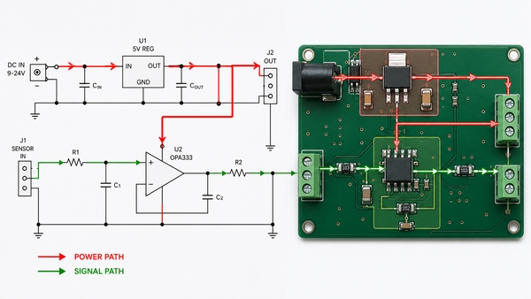
The aluminum base gives the PCB strength. It also spreads heat away from hot parts.
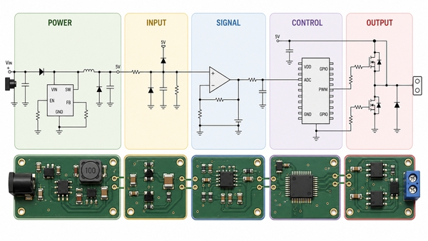
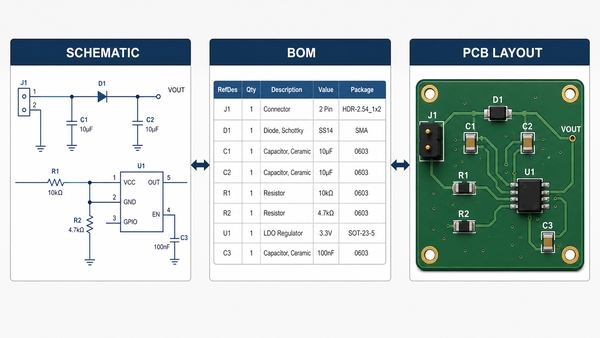
Aluminum ThicknessCommon Use
0.8 mmLight LED modules
1.0 mmGeneral lighting products
1.5 mmCommon aluminum PCB design
2.0 mm or aboveHigh-power or rugged products

For many LED boards, 1.5 mm is a common choice. However, larger lamps and industrial products may need 2.0 mm or thicker aluminum.

Solder Mask and Surface Finish

White solder mask is common for LED aluminum PCB. It reflects light better than dark solder mask. As a result, it helps improve light output.

Common surface finishes include lead-free HASL, ENIG, OSP, and immersion silver. For example, lead-free HASL is often used for standard LED boards. However, ENIG is better when the board needs a flat surface or fine-pitch parts.

aluminum-pcb-layer-structure

What Are the Common Aluminum PCB Stackup Types?

The most common aluminum PCB is single-sided. However, double-sided and hybrid aluminum PCBs are also used. The right choice depends on heat, current, routing space, and cost.

Single-Sided Aluminum PCB

Single-sided aluminum PCB is the most popular type. The circuit and parts are on one side. The aluminum base is on the other side.It is often used in:

  • LED bulbs
  • Street lights
  • High-bay lights
  • Panel lights
  • Power modules
  • Simple driver boards

Also, this type is cost-effective. It gives heat a short path to the aluminum base.

Double-Sided Aluminum PCB

Double-sided aluminum PCB has circuits on both sides. It gives more space for routing. Therefore, it is useful when the circuit is more complex.

However, it is harder to produce than a single-sided board. The via structure and insulation must be controlled well.

Hybrid Aluminum PCB

Hybrid aluminum PCB combines FR4 layers with an aluminum base. It is useful when a product needs both signal routing and heat control.

For example, FR4 can handle control signals. Meanwhile, aluminum can help remove heat from the power section.

What Thermal Conductivity Should You Choose for Aluminum PCB?

The right thermal conductivity depends on the product. For many LED products, 1.0–1.5 W/m·K is enough. However, high-power products often need 2.0 W/m·K or more.

Thermal ConductivitySuitable UseSimple Advice
1.0 W/m·KLow-power LED productsGood for simple lighting
1.5 W/m·KStandard LED lightingCommon choice
2.0 W/m·KMedium-power LED and power boardsBetter for more heat
3.0 W/m·K or higherHigh-power LED, automotive, industrial boardsGood for demanding designs

Higher thermal conductivity can move heat faster. However, it is not the only factor. Copper thickness, dielectric thickness, pad design, and heat sink contact also matter.

Therefore, do not choose material only by price. Also, do not choose the highest value without checking the real heat load.

For sealed lamps, automotive lights, medical devices, and industrial modules, it is better to leave more safety margin. As a result, the product can work more safely over time.

How Should You Design an Aluminum PCB Circuit Board Layout?

A good aluminum PCB layout should control heat, current, insulation, and mounting. The board is not only a circuit carrier. It is also part of the heat system.

Place Hot Parts Properly

High-power LEDs, MOSFETs, regulators, drivers, and power resistors should not be packed into one small area.

If hot parts are too close, hot spots may appear. As a result, some parts may age faster.

Therefore, spread hot parts when the circuit allows it. This helps the aluminum base spread heat more evenly.

Use Wider Copper for High Current

High-current traces should not be too narrow. Narrow copper creates more resistance. As a result, it creates more heat.

For high-current areas, use:

  • Wider traces
  • Copper pours
  • Thicker copper
  • Shorter current paths
  • Better thermal pads

Also, copper balance is important in LED arrays. Uneven copper may affect heat flow and soldering quality.

Design Thermal Pads Well

Thermal pads help move heat from components into the PCB. For LEDs and power parts, the pad should be large enough.

Also, the pad should connect well to the copper area. As a result, the LED junction temperature can be lower.

Control Clearance and Creepage

The aluminum base is conductive. Therefore, insulation design is very important.

Check these areas:

  • High-voltage spacing
  • Board edge clearance
  • Mounting hole isolation
  • Connector spacing
  • Exposed aluminum areas
  • Screw contact points

This is very important for LED drivers, medical power boards, industrial power supplies, and automotive electronics.

Design Mounting Holes Carefully

Mounting holes affect both strength and safety. If screws touch the aluminum base, the design must confirm whether the base is grounded or isolated.

In many products, screws press the PCB against a heat sink. This helps heat transfer. However, the structure must not damage the insulation layer.

What Are the Advantages and Disadvantages of Aluminum PCBs?

Aluminum PCBs offer strong heat control and good strength. However, they also have some limits. For example, they cost more than basic FR4 boards. Also, they are not ideal for very dense multilayer routing.

ItemAdvantagesLimits
Heat ControlGood for LED and power productsDepends on dielectric quality
StrengthRigid and stableNot flexible
CostGood value for heat productsHigher than standard FR4
DesignGood for simple power circuitsHarder for dense routing
ReliabilityReduces heat stressNeeds correct material choice
ReworkStable after assemblyRework may be harder

The main benefit is heat control. If heat affects your product, aluminum PCB is often a good choice.

However, the board must match the real use. A high-power street light should not use the same material as a small decorative lamp. Therefore, material selection should be based on heat load, current, and working environment.

What Are Aluminum PCBs Used For?

Aluminum PCBs are used in products that need fast and stable heat transfer. They are common in LED lighting, power electronics, automotive electronics, industrial equipment, medical devices, and aerospace systems.

LED Lighting

LED lighting is one of the largest markets for aluminum PCB.Common products include:

  • LED bulbs
  • LED tubes
  • Street lights
  • High-bay lights
  • Stage lights
  • UV LED modules
  • Panel lights
  • Automotive LED lamps

In LED products, aluminum PCB helps control heat near the LED chip. As a result, it supports stable brightness and longer life.

Power Electronics

Power electronics often create high heat in small spaces. Therefore, aluminum PCB can help reduce heat build-up.

Typical products include power supplies, DC-DC converters, motor drivers, inverters, voltage regulator modules, and charging modules.

Automotive Electronics

Automotive electronics must work under heat, vibration, and long use.

Aluminum PCBs are often used in LED headlights, taillights, signal lights, interior lighting, power modules, and battery-related boards.

Industrial Equipment

Industrial products often run for long hours. Therefore, stable heat control is important.

Aluminum PCBs can be used in automation equipment, industrial LED indicators, power modules, control cabinets, motor control boards, and machine vision lighting.

Medical and Aerospace Electronics

Medical and aerospace products often need stable heat behavior and strong process control.

Aluminum PCB may be used in medical lighting, diagnostic modules, UAV electronics, aerospace lighting, and compact power boards.

In these fields, traceability, inspection records, and stable quality are also important.

Why Are Aluminum PCBs Popular in LED Lighting?

led-aluminum-pcb

Aluminum PCBs are popular in LED lighting because LEDs create heat during use. If the heat is not removed well, brightness and life may drop.

An LED does not turn all electric energy into light. Some energy becomes heat. If this heat stays near the LED chip, the junction temperature rises.

High junction temperature may cause:

  • Lower light output
  • Faster lumen loss
  • Color shift
  • Shorter service life
  • More solder joint stress

Therefore, aluminum PCB is a strong choice for LED lighting. It creates a shorter heat path from the LED package to the lamp housing or heat sink.

Design ItemCommon Choice
Board TypeSingle-sided aluminum PCB
Board Thickness1.5 mm
Copper Thickness1 oz or 2 oz
Solder MaskWhite
Surface FinishLead-free HASL or ENIG
Thermal Conductivity1.5–2.0 W/m·K

White solder mask is common in LED aluminum PCB. It reflects light better than dark solder mask. Therefore, it supports both heat control and light output.

For high-power street lights, industrial lights, and automotive lamps, higher thermal conductivity and thicker copper may be needed.

Aluminum PCB Circuit Board vs FR4 PCB: Which Is Better?

Aluminum PCB is better for heat control. However, FR4 PCB is better for complex routing and low-heat circuits. Therefore, the better choice depends on your design goal.

Comparison ItemAluminum PCB Circuit BoardFR4 PCB
Base MaterialAluminum metal baseFiberglass epoxy
Heat ControlStrongLimited
Best UseLED, power, automotive lightingSignal, control, digital circuits
Circuit ComplexityBetter for simple heat designsBetter for multilayer routing
StrengthStrong and rigidGood for general electronics
CostHigher than basic FR4Lower for standard boards
Extra Heat SinkOften less neededOften needed for high power
Common ProductsLED lighting, power modules, industrial equipmentConsumer electronics, control boards

Choose aluminum PCB when heat is the main issue. It is suitable for LEDs, power modules, automotive lamps, and compact heat-sensitive products.

However, choose FR4 when the design needs many signal layers, fine-pitch IC routing, lower heat, and lower standard PCB cost.

In many products, both boards can be used together. For example, FR4 can handle signal control. Meanwhile, aluminum PCB can handle the LED or power section.

How to Select the Most Appropriate Aluminum PCB for Your Needs

To select the right aluminum PCB, start with heat load, current, voltage, environment, structure, and service life. Do not choose only by board thickness or price.

Check Heat Load First

Before selecting material, check:

  • Component power
  • Operating current
  • Ambient temperature
  • Enclosure design
  • Heat sink contact
  • Working hours
  • Product life target
  • Safety needs

A sealed outdoor lamp needs more heat margin than an open indoor module.

Select Thermal Conductivity

Match the thermal conductivity with the real use. For standard lighting, 1.5 W/m·K may be enough. However, compact high-power designs may need 2.0 W/m·K or higher.

Choose Copper Thickness

Copper thickness should match the current path. If the board carries higher current, use thicker copper or wider copper areas.

Otherwise, thin traces may create extra heat, even when the aluminum base is good.

Match Surface Finish

If the board uses simple LED packages, lead-free HASL may work well. However, if the board uses fine-pitch parts or needs a flatter surface, ENIG is often better.

Request DFM Review

A DFM review can find design and production risks before fabrication.

It should check trace width, spacing, mounting holes, thermal pads, solder mask openings, board edge clearance, surface finish, and assembly needs.

Finally, for high-power, automotive, medical, or industrial products, early review can reduce redesign cost and improve production stability.

EBEST Circuit: A Reliable Aluminum PCB Manufacturer

EBEST supports aluminum PCB fabrication, DFM review, component sourcing, PCBA assembly, and testing for heat-control electronic products.

For aluminum PCB projects, EBEST can review material choice, copper thickness, dielectric performance, solder mask, surface finish, layout risk, and assembly process before production.

EBEST Circuit CapabilityCustomer Value
Aluminum PCB FabricationSupports LED, power, automotive, industrial, and heat-control designs
DFM ReviewHelps reduce layout and production risks
PCB + PCBA ServiceSupports fabrication, sourcing, assembly, and testing
Material Selection SupportHelps match heat needs and board structure
Prototype to Batch ProductionSupports design test and production growth
Quality InspectionImproves consistency and delivery confidence

EBEST supports aluminum PCB projects for LED lighting, industrial equipment, automotive electronics, medical devices, aerospace modules, communication equipment, and power electronics.

Also, early manufacturing feedback can help customers reduce redesign work and improve delivery speed.

If you need an aluminum PCB circuit board, aluminum PCB assembly, or related PCB manufacturing support, EBEST can help from DFM review and PCB fabrication to component sourcing, assembly, and final testing. For project review or quotation support, contact sales@bestpcbs.com.

You may also like

Custom PCB Design and Fabrication Services
Friday, February 20th, 2026

Looking for custom PCB design and fabrication services? This guide covers services, processes, DFM principles and quotes to help you find reliable custom solutions.

What Is PCB Designing and Fabrication?

PCB designing and fabrication transforms an electronic concept into a reliable, build-ready circuit board through a tightly connected engineering process. It begins with schematic design and layout planning, where signal paths, power flow, and component placement are carefully arranged. From there, the design is converted into precise manufacturing data that guides copper etching, layer lamination, drilling, and surface finishing. When design intent and fabrication capability are aligned early, the result is a board that performs as expected and moves smoothly into assembly.

At the same time, successful PCB designing and fabrication depends on practical decisions, not just electrical theory. Material selection, stack-up balance, and manufacturability checks all play a role in controlling cost and quality. Clear documentation and early DFM reviews help avoid rework and schedule delays. By treating design and fabrication as one continuous workflow, teams can achieve faster turnaround, higher yield, and more predictable production outcomes.

What Is PCB Designing and Fabrication, https://www.bestpcbs.com/blog/2026/01/custom-pcb-design-and-fabrication-services/

Types of Custom PCB Design and Fabrication Services

Custom PCB design and fabrication services cover diverse project needs, with specialized options for every stage. Prototype services handle low-volume orders (1-100 units) for design validation. They offer fast turnaround (24-72 hours) to speed up your testing cycles and allow quick iterations.

Small-batch fabrication (100-5,000 units) balances speed and cost. It suits niche products or pre-market launches, with flexible surface finishes and material choices. High-volume production (5,000+ units) uses automated workflows for consistency and efficiency, ideal for mass-market products.

Additionally, specialized services cater to complex needs. These include HDI (High-Density Interconnect) boards for compact devices and high-frequency PCBs for RF applications. Rigid-flex PCBs and automotive-grade options (compliant with IATF 16949) are also available for targeted industries.

PCB Design and Fabrication Process

Below are PCB design and fabrication process for your reference:

1. Design Phase: Schematic Capture & Layout

  • Schematic Design: Begin with accurate schematic creation using tools like Altium Designer, OrCAD, or KiCad. Ensure component libraries adhere to IPC standards for consistency.
  • PCB Layout: Translate schematics into a physical layout, prioritizing signal integrity (e.g., controlled impedance routing, minimizing EMI via proper ground planes). Use design rule checks (DRC) to validate clearance, trace width, and differential pair spacing.
  • Advanced Techniques: For HDI designs, incorporate microvias (0.1mm or smaller) and blind/buried vias to optimize space. Flexible PCBs require specialized material selection and bend-radius calculations.

2. Material Selection & Stackup Design

  • Substrate Materials: Choose FR-4 for cost-effective rigid boards, polyimide for flex circuits, or high-frequency laminates (e.g., Rogers RO4350B) for RF applications. Consider thermal management needs with materials like aluminum-core boards.
  • Copper Weight & Thickness: Select copper weights (0.5oz to 4oz) based on current-carrying requirements. Thicker copper enhances thermal dissipation but increases cost.
  • Stackup Configuration: Define layer count and sequence (signal, power, ground layers) to minimize crosstalk. Use symmetric stackups for warpage control during fabrication.

3. Imaging, Etching & Plating

  • Photolithography: Apply photoresist, expose to UV through artworks, and develop to create circuit patterns. Modern LDI (Laser Direct Imaging) eliminates film usage, enhancing precision.
  • Etching: Use ammonia-based etchants for copper removal, ensuring precise trace edges. Acid-copper plating follows to deposit thick copper in vias and pads.
  • Via Processing: Mechanical drilling for standard vias; laser drilling for microvias. Copper plating via holes ensures electrical continuity.

4. Surface Finish & Solderability

  • HASL (Hot Air Solder Leveling): Traditional tin-lead or lead-free finish for through-hole components.
  • ENIG (Electroless Nickel Immersion Gold): Ideal for fine-pitch SMT pads, wire bonding, and aluminum wire connections. Provides excellent shelf life.
  • OSP (Organic Solderability Preservative): Cost-effective for short-term storage, but less durable than ENIG.
  • Immersion Silver/Tin: For high-frequency applications to maintain signal integrity.

5. Drilling, Routing & Mechanical Processing

  • CNC Drilling: Precision drilling of via holes and mounting holes. Use peck drilling to prevent tool wear.
  • Routing & Profiling: CNC routing machines cut board outlines and internal slots. V-scoring enables easy separation of panelized boards.
  • Beveling & Countersinking: Chamfer edges for assembly safety; countersink holes for flush screw heads.

6. Inspection, Testing & Quality Assurance

  • AOI (Automated Optical Inspection): Detects solder mask defects, missing pads, and trace misalignment.
  • X-ray & CT Inspection: For hidden defects like voids in BGA solder joints or buried via integrity.
  • Electrical Testing: Flying probe or in-circuit testers verify connectivity. Use netlist comparison to catch opens/shorts.
  • Environmental Testing: Thermal cycling, humidity testing, and vibration tests ensure reliability under operational conditions.

7. Assembly Integration & Soldering

  • SMT (Surface Mount Technology): Stencil printing, pick-and-place machines, and reflow ovens assemble dense components. Nitrogen reflow reduces oxidation.
  • Through-Hole Assembly: Wave soldering for traditional components; selective soldering for mixed-technology boards.
  • Conformal Coating: Protect against moisture, dust, and chemicals. Acrylic, silicone, or parylene coatings are common.
PCB Design and Fabrication Process, https://www.bestpcbs.com/blog/2026/01/custom-pcb-design-and-fabrication-services/

    DFM Principles to Optimize PCB Design for Fabrication

    • Keep trace widths and spacing consistent: Use 6mil/6mil minimum for standard boards and 3mil/3mil for HDI, with ±10% tolerance for precision. HDI designs typically add 15%-20% to production costs.​
    • Route traces at least 12mil away from chip pads: Maintain ≥2mil green oil bridges between pads to prevent soldering defects during assembly.​
    • Standardize hole sizes to 0.15mm-1.0mm range: Control non-plated hole tolerance at ±2mil to reduce tooling changes and cut drilling time by 30%.​
    • Maintain 12mil distance between vias and pads: Use square board edges and 3mm clearance from components, with ≥1mm rounded corners for stability.​
    • Use 45 or 90-degree angles for traces near pads: Avoid angles below 30 degrees, as they trap acid and accelerate copper corrosion after 30+ hours in humid environments.​
    • Add test points early with 1.0mm-1.2mm diameter: Space them ≥70mil apart and keep 125mil clearance from board edges for post-assembly testing.​
    • Incorporate DFM reviews within 24 hours of design finalization: These checks reduce rework risks by 30%+ and align layouts with fabrication capabilities upfront.
    DFM Principles to Optimize PCB Design for Fabrication, https://www.bestpcbs.com/blog/2026/01/custom-pcb-design-and-fabrication-services/

    Material Selection Strategies for Custom PCB Design and Fabrication

    Material selection directly impacts PCB performance and production efficiency. PCB design and fabrication relies heavily on proper material matching, so follow these targeted strategies:

    • General-purpose projects choose FR-4: Optimize for UL94 V-0 flame-retardant grades with Tg 130-140℃. Its Dk 4.2-4.8 (1MHz) and Df 0.020-0.025 fit consumer electronics and industrial controls.​
    • High-frequency (1GHz+) use specialized substrates: Pick PTFE or Rogers materials for stable Dk values and minimal signal loss. RO5880 suits 77GHz automotive radar; RO3003 works for GPS and base station antennas.​
    • High-temperature applications need high-Tg substrates: Select variants with Tg ≥150℃ to resist reflow soldering deformation. High-multilayer boards require Tg 170-180℃+ for industrial and automotive use.​
    • Match surface finishes to assembly needs: ENIG (4-8μm nickel, 0.05-0.1μm gold) fits fine-pitch components and long storage. HASL offers cost-effectiveness for general use; OSP suits lead-free tight-pitch designs.​
    • Adapt to harsh environments: Use high-CTI FR4 for high-voltage moist settings. Prioritize materials with strong thermal conductivity for high-power or extreme-temperature scenarios.​
    • Align with impedance control goals: For 50Ω/75Ω impedance requirements, coordinate substrate Dk with trace width and dielectric thickness. This ensures signal integrity in high-speed designs.

    Quality Control and Testing Methods in PCB Design and Fabrication

    Strict quality control (QC) guarantees consistent, reliable PCB design and fabrication results. Implement these targeted testing methods for comprehensive validation:​

    • Flying Probe Electrical Testing: Check for open/short circuits with 95%+ coverage. Maintain contact resistance below 10mΩ for accurate results across all layers.​
    • TDR Impedance Testing: Control impedance tolerance within ±10% for high-frequency boards. Narrow to ±7% for 5G and DDR fast-data applications to preserve signal integrity.​
    • AOI Visual Inspection: Use automated optical equipment to detect 0.05mm micro-defects. Catch trace blemishes, solder joint issues and component misalignment per IPC-A-600 standards.​
    • Thermal Cycling Testing: Subject boards to 40℃ below zero to 125℃ cycles. Complete 3 rounds of 288℃ solder dipping for 10 seconds each to test temperature resistance.​
    • Humidity Cycling Testing: Validate stability in moist conditions. Run 85℃/85%RH cycles for 1000 hours to ensure no layer separation or insulation degradation.​
    • Ion Contamination Testing: Keep post-fabrication residue below 5μg/in². Use eco-friendly cleaning agents to prevent corrosion and extend board lifespan.
    Quality Control and Testing Methods in PCB Design and Fabrication, https://www.bestpcbs.com/blog/2026/01/custom-pcb-design-and-fabrication-services/

    Common Pitfalls & Solutions in PCB Design and Fabrication

    Pitfall 1: Pad and Aperture Mismatch. This causes drill breakage and circuit defects.
    Solution 1: Use DRC tools to validate coordinates early. Control aperture tolerance at ±2mil, standardize pad markings and set pad size 0.2mm larger than hole diameter.

    Pitfall 2: Unclear Layer Stackup. This triggers signal interference and EMI.
    Solution 2: Label layers sequentially and keep signal layers adjacent to ground planes. Design even-layer stacks symmetrically to prevent high-temperature deformation.

    Pitfall 3: Inadequate Component Spacing. This leads to soldering flaws and thermal issues.
    Solution 3: Maintain ≥0.5mm minimum spacing. Keep high-power devices 5mm+ from precision components and use differential pair routing for high-speed signals.

    Pitfall 4: Incomplete Gerber Files. This results in misfabrication.
    Solution 4: Export RS-274X format files covering all layers. Conduct pre-fabrication reviews with your provider to verify data integrity before production.

    Pitfall 5: Asymmetric Layer Lamination. This causes board warpage after reflow.
    Solution 5: Adopt symmetric stackup for even-layer boards. Add dummy copper to balance stress for odd-layer designs and match material thermal expansion coefficients.

    Pitfall 6: Poor High-Speed Signal Routing. This degrades signal integrity.
    Solution 6: Route differential pairs with consistent 50Ω/75Ω impedance. Keep pair spacing 3-5mil and avoid sharp bends to reduce noise interference.

    Why Choose EBest(Best Technology) for Custom PCB Design and Fabrication Partner?

    Reasons why choose EBest(Best Technology) for custom PCB design and fabrication partner:

    • 19 Years of Professional Expertise: We’ve specialized in custom PCB production since 2006, serving over 4000 global clients. Having delivered more than 1.2 million custom PCBs, we cater to high-end sectors like aerospace, automotive and medical.​
    • 24-Hour Rapid Prototyping and Delivery: 1-8 layer standard PCB prototypes ship within 24 hours, including full electrical testing and AOI inspection. Small-batch orders (100-500 units) deliver in 48 hours with a 99.2% on-time rate to speed up your project cycles.​
    • Sample & Small-Batch Customization Capacity: Support 1-piece sample orders and 1-5000 units small-batch customization. Custom types cover 1-24 layer boards, HDI, ceramic PCBs, rigid-flex and automotive/medical-grade options with full parameter tailoring.
    • Strict Quality Control with Authoritative Certifications: Boast ISO9001, AS9100D (aerospace) and IATF 16949 (automotive) certifications. Execute 18 rigorous QC processes to keep product yield consistently above 99.5%.​
    • One-Stop PCBA Custom Services: Offer integrated custom PCB fabrication, BOM procurement, SMT assembly (precision ±0.03mm) and functional testing. Tailor solutions to cut multi-party communication costs and streamline workflows.​
    • MES System for Full-Process Traceability: Track production nodes, process parameters and inspection data in real time via MES. Enjoy end-to-end batch traceability with 3 years of data retention for compliance and accountability.​
    • Flexible Customized Solutions: Adapt processes to meet special requirements like high-voltage ceramic PCBs and ultra-thin HDI boards. Offer 1-on-1 technical consultation to optimize custom designs and accelerate project success.

    Welcome to contact us if you have any request for PCB design and fabrication services: sales@bestpcbs.com.

    You may also like

    PCB Design and Fabrication, One-Stop PCB Solution Supplier
    Tuesday, June 24th, 2025

    Looking for PCB Design and fabrication solutions? This guide explores design flaw detection, signal integrity solutions, cost-effective fabrication, and integrated service selection for efficient PCB development.

    EBest Circuit (Best Technology) solves these challenges with our reliable one-stop PCB design and fabrication services. We offer free DFM analysis to eliminate 90% of manufacturing issues before production begins, saving you time and money on reworks. For urgent needs, our 24-hour rapid prototyping service delivers with 98% on-time accuracy—no more missed deadlines. Whether you need 1-piece prototypes or high-volume orders, we handle everything from complex HDI and high-speed boards to RF designs, backed by 18+ years of specialized experience. Every PCB undergoes 100% inspection using advanced AOI and flying probe testing, ensuring defect rates below 500ppm. With transparent pricing (typically 15-20% more cost-effective than competitors) and no hidden fees, we make budgeting predictable. Over 1,200 global clients trust us to combine precision engineering with fast turnaround. Submit your design today for a risk-free quote within 24 hours and experience stress-free PCB manufacturing: sales@bestpcbs.com.

    What Is PCB Design?

    PCB design is the process of planning and arranging electronic circuits on a board to create functional connections. Engineers begin by drafting a schematic to map out how components should link together, then carefully position each part and draw conductive pathways between them. This stage requires attention to both electrical behavior, like maintaining clean signals and stable power flow, and physical limitations such as board dimensions and layer arrangements. Designers follow specific manufacturing guidelines for trace widths, hole placements, and material choices to guarantee the board can be reliably produced. More complex designs might need specialized techniques for handling fast signals, matching impedance, or managing heat buildup. A well-executed PCB design transforms circuit ideas into practical, manufacturable boards that power devices ranging from everyday gadgets to advanced industrial equipment. For streamlined development, services combining design and fabrication help align creative choices with production realities from the start.

    What Is PCB Design?

    How to Catch PCB Design Flaws Early to Prevent Project Halts?

    • Leverage Design Rule Checks (DRC)‌: Run automated DRC tools at every major design milestone. Configure rules to match fabrication capabilities (e.g., minimum trace width, clearance). Address violations immediately to avoid compounding errors.
    • Simulate Before Prototyping‌: Use signal integrity (SI) and power integrity (PI) simulations for high-speed designs. Identify issues like crosstalk or voltage drops early, reducing costly re-spins.
    • Cross-Functional Reviews‌: Organize collaborative reviews with layout engineers, firmware developers, and manufacturers. Fresh perspectives often reveal overlooked gaps (e.g., thermal management, testability).
    • Test Point Accessibility‌: Ensure test points are logically placed and unobstructed. This simplifies debugging and avoids post-production surprises.
    • Component Footprint Validation‌: Double-check footprints against datasheets before finalizing the layout. Mismatched pads or 3D model collisions can halt assembly.
    • Thermal Analysis‌: Model heat dissipation for power components. Poor thermal design leads to field failures, especially in compact layouts.
    • DFM/DFA Audits‌: Partner with fabricators to review design-for-manufacturability (DFM) and assembly (DFA) guidelines. Adjustments like solder mask spacing can prevent yield losses.
    • Early Prototyping‌: Order small-batch prototypes to validate physical performance. Functional testing at this stage exposes flaws masked in simulations.
    • Version Control & Documentation‌: Maintain clear revision logs and annotate design changes. Confusion over file versions often causes delays.
    • Supply Chain Alignment‌: Verify component availability and lifecycle status during design. Last-minute substitutions due to obsolete parts derail timelines.

    How to Prevent Signal Integrity and Crosstalk Issues in High-Speed PCB Design?

    Methods about how to prevent signal integrity and crosstalk issues in high-speed PCB design:

    • Prioritize Controlled Impedance Traces: Maintain consistent impedance across high-speed signal paths by defining precise trace widths, dielectric thicknesses, and copper weights. Use impedance calculation tools during layout planning to align with your PCB stack-up design. Consistent impedance reduces reflections and ringing, which are common causes of signal degradation.
    • Optimize Trace Routing and Spacing: Route high-speed signals on dedicated layers with continuous ground planes beneath them to minimize electromagnetic interference (EMI).Increase the spacing between aggressive (aggressor) and victim traces to reduce crosstalk. A rule of thumb is to maintain a gap of at least three times the trace width between parallel runs.
    • Implement Differential Pair Routing: Use differential pairs for high-speed differential signals (e.g., USB, HDMI, PCIe) to enhance noise immunity. Route pairs symmetrically with matched lengths and equal spacing to preserve signal balance. Avoid inserting vias or stubs into differential pairs, as these disrupt impedance continuity.
    • Limit Parallel Trace Lengths: Minimize the length of parallel trace segments between unrelated signals. Crosstalk severity increases with both parallel length and signal rise time. If parallel routing is unavoidable, use guard traces (connected to ground) between aggressors and victims to absorb unwanted coupling.
    • Choose Low-Loss Dielectric Materials: Select PCB laminates with low dielectric constants (Dk) and low dissipation factors (Df) to reduce signal attenuation and phase distortion at high frequencies. Materials like FR4-grade laminates with optimized resin systems strike a balance between cost and performance for mid-range speeds.
    • Incorporate Proper Termination Strategies: Apply series or parallel termination resistors at the source or receiver ends of high-speed traces to match impedance and dampen reflections. For multi-drop buses, use AC-coupled termination to accommodate varying voltage levels without signal distortion.
    • Validate Designs with Pre-Layout Simulations: Perform SI simulations early in the design cycle to predict issues like overshoot, undershoot, and ringing. Tools like IBIS models or SPICE simulators help evaluate driver/receiver behavior and identify required adjustments before finalizing the layout.
    • Use Post-Layout Extraction and Analysis: After routing, extract the PCB’s parasitic elements (e.g., capacitance, inductance) and re-simulate to validate performance under real-world conditions. Address discrepancies by tweaking trace geometry, termination, or topology.
    • Isolate Noisy and Sensitive Circuits: Separate high-speed digital circuits from analog or low-noise components (e.g., RF modules, sensors) using ground planes or isolation trenches. This reduces EMI and prevents noise coupling into vulnerable sections.
    • Collaborate with Manufacturers for DFM Input: Share your design with your PCB fabricator early to leverage their expertise in high-speed materials and stack-up configurations. They can advise on feasible trace/space tolerances, via structures, and impedance control methods aligned with their production capabilities.
    • Test Prototypes with Advanced Validation Tools: During prototyping, use time-domain reflectometry (TDR) or bit-error-rate testing (BERT) to validate signal quality. These tests uncover hidden SI issues like impedance discontinuities or jitter that simulations might miss.
    • Document and Enforce Design Guidelines: Create a checklist of SI/crosstalk rules tailored to your project’s speed and complexity. Train your team to follow these guidelines consistently, reducing variability and rework.
    How to Prevent Signal Integrity and Crosstalk Issues in High-Speed PCB Designs?

    How to Handle Frequent Design Changes without Increasing Project Time and Expenses?

    Here are ways about how to handle frequent design changes without increasing project time and expenses:

    • Design for Consistent Impedance: Calculate and maintain precise impedance values across all high-speed traces. Use impedance calculation tools during layout planning to define trace widths, dielectric thicknesses, and copper weights that align with your PCB stack-up. Consistent impedance minimizes reflections and ringing, which are primary causes of signal degradation.
    • Route Traces Strategically: Avoid parallel routing of unrelated signals whenever possible. If parallel traces are unavoidable, limit their length and increase the spacing between them (ideally three times the trace width). Additionally, incorporate guard traces connected to ground between potential aggressor and victim nets to absorb unwanted noise.
    • Adopt Differential Pair Routing: For differential signals (e.g., USB 3.0, HDMI, Ethernet), route pairs symmetrically with matched lengths and fixed spacing. This approach enhances noise immunity and reduces susceptibility to common-mode interference. Avoid vias or stubs in differential pairs to preserve signal integrity.
    • Choose Low-Loss Dielectric Materials: Select PCB laminates with low dielectric constants (Dk) and dissipation factors (Df) to minimize signal loss at high frequencies. Materials like FR4-grade laminates with optimized resin systems offer a balance between cost and performance for mid-range speed requirements.
    • Implement Proper Termination: Apply series or parallel termination resistors at the source or receiver ends of high-speed traces to match impedance and dampen reflections. For multi-drop buses, consider AC-coupled termination to accommodate varying voltage levels without distortion.
    • Simulate Early and Iterate: Perform pre-layout SI simulations to predict issues like overshoot, undershoot, and ringing. After routing, extract parasitic elements and re-simulate to validate performance under real-world conditions. Address discrepancies by adjusting trace geometry, termination, or topology.
    • Isolate Sensitive Circuits: Separate high-speed digital circuits from analog or low-noise components (e.g., RF modules, sensors) using ground planes or isolation trenches. This reduces electromagnetic interference (EMI) and prevents noise coupling into vulnerable sections.
    • Collaborate with Your Fabricator: Share your design with your PCB manufacturer early to align with their production capabilities. They can advise on feasible trace/space tolerances, via structures, and impedance control methods, avoiding costly rework later.
    • Validate with Advanced Testing: During prototyping, use tools like time-domain reflectometry (TDR) or bit-error-rate testing (BERT) to uncover hidden SI issues. These tests provide critical insights into impedance discontinuities or jitter that simulations might miss.
    • Document and Enforce Design Rules: Create a checklist of SI/crosstalk guidelines tailored to your project’s needs. Train your team to follow these rules consistently, reducing variability and ensuring high-quality outcomes.

    What Is PCB Fabrication?

    PCB fabrication is the manufacturing process that transforms circuit board designs into physical, functional products ready for component assembly. Beginning with a substrate material, the process involves precise copper patterning to create conductive pathways, followed by laminating insulating layers, drilling holes for vias and component leads, and applying protective solder mask and silkscreen. Each step requires careful attention to design specifications to ensure proper electrical connectivity, thermal management, and mechanical reliability. Advanced fabrication techniques accommodate high-density interconnects, controlled impedance for high-speed signals, and specialized materials for challenging environments. By maintaining strict quality control throughout production, manufacturers deliver boards that perform as intended while meeting cost and timeline expectations – ultimately reducing development risks for engineers and enabling smoother transitions from prototype to mass production.

    What Is PCB Fabrication?

    How to Choose A One-Stop PCB Solution Supplier For Your PCB Fabrication Project?

    Tips about one-stop PCB solution supplier selection:

    • Evaluate Technical Expertise and Capabilities: Begin by assessing whether the supplier offers end-to-end services, including design assistance, prototyping, fabrication, assembly, and testing. Ensure they support your project’s complexity, whether it involves rigid boards, flex circuits, HDI, or advanced materials. A supplier with in-house engineering teams can preemptively address DFM (Design for Manufacturability) issues, saving you time and rework costs.
    • Verify Quality Certifications and Standards: Prioritize suppliers with certifications like ISO 9001, IPC-A-600, and UL recognition. These certifications demonstrate adherence to global quality and safety standards, reducing the risk of defects or compliance issues. Request samples or case studies to evaluate their workmanship, especially for high-speed or high-reliability applications.
    • Assess Production Capacity and Flexibility: Confirm the supplier’s ability to scale production to meet your volume needs, from prototypes to mass production. Inquire about their equipment’s precision (e.g., laser drilling for microvias) and material inventory to handle lead-free RoHS-compliant processes or specialized laminates. Flexibility in accommodating rush orders or design changes can prevent project delays.
    • Compare Pricing and Transparency: Request detailed quotes that break down costs for design, materials, fabrication, assembly, and testing. Beware of hidden fees for services like stencils or impedance control. A transparent supplier will explain cost drivers, such as layer count or tight tolerances, helping you optimize design choices without sacrificing performance.
    • Review Turnaround Time and Logistics: Shorten your time-to-market by choosing a supplier with fast prototyping lead times (e.g., 24–48 hours for bare boards). Inquire about their global shipping capabilities, customs clearance support, and inventory management for consigned components. A supplier with local facilities can reduce shipping costs and delivery times.
    • Seek Customer References and Reviews: Contact the supplier’s existing clients to gauge their reliability, communication, and problem-solving efficiency. Look for testimonials highlighting their responsiveness during crises, such as component shortages or design emergencies. A supplier with a proven track record in your industry (e.g., automotive, medical) will better understand your regulatory needs.
    • Leverage Design Support and DFM Reviews: Prioritize suppliers offering free DFM checks before fabrication. This service identifies issues like impossible trace widths, insufficient solder mask clearance, or panelization inefficiencies, preventing costly re-spins. Some suppliers also provide signal integrity simulations or thermal management guidance, adding value beyond basic manufacturing.
    • Ensure Component Sourcing Reliability: If outsourcing assembly, confirm the supplier’s access to authorized component distributors to avoid counterfeit parts. Inquire about their strategies for mitigating obsolescence or supply chain disruptions, such as maintaining safety stock or cross-referencing alternatives.
    How to Choose A One-Stop PCB Solution Supplier For Your PCB Fabrication Project?

    How to Ensure On-Time Delivery for PCB Fabrication Orders with Complex Specifications?

    Here are ways about how to speed up the process of PCB fabrication orders with complex specifications:

    • Conduct a Thorough Pre-Production Technical Review: Engage your supplier early to review design files, material specifications, and tolerance requirements. A detailed technical audit identifies potential manufacturing bottlenecks, such as impossible microvia dimensions or incompatible laminate choices, before production begins. Addressing these upfront prevents costly rework later.
    • Establish Clear Milestones and Deadlines: Break the project into phases (e.g., design finalization, prototyping, tooling, mass production) with defined deliverables and timelines. Use project management tools to track progress and hold regular check-ins with your supplier. Visibility into each stage ensures accountability and enables swift corrective actions if delays emerge.
    • Prioritize Suppliers with Advanced Manufacturing Capabilities: Select a supplier equipped to handle complex specifications, such as HDI boards, rigid-flex designs, or embedded components. Inquire about their machinery precision (e.g., laser drills for microvias), material inventory, and experience with similar projects. A technically capable partner reduces iterations and accelerates production.
    • Leverage Parallel Workstreams: Overlap non-dependent tasks to compress schedules. For example, initiate component sourcing or stencil fabrication while awaiting prototype test results. This approach minimizes idle time and keeps the project moving forward.
    • Implement Real-Time Communication Channels: Establish direct, frequent communication with your supplier’s project manager via shared platforms (e.g., Slack, Microsoft Teams) or daily stand-up meetings. Immediate access to decision-makers resolves issues like design clarifications or material substitutions quickly, preventing delays from back-and-forth emails.
    • Secure Component Availability Early: If outsourcing assembly, confirm component lead times and lock in orders with authorized distributors well in advance. For long-lead-time or obsolete parts, collaborate with your supplier to identify alternatives or pre-book inventory. This proactive step avoids production halts due to missing components.
    • Perform Staged Quality Inspections: Schedule interim quality checks during fabrication (e.g., after layer stacking, etching, or solder mask application) rather than waiting for final inspection. Early detection of issues like layer misalignment or impedance deviations allows timely corrections without derailing the timeline.
    • Build Flexibility into Logistics: Partner with logistics providers offering expedited shipping options and real-time tracking. For critical orders, negotiate guaranteed delivery windows or use air freight as a backup. Having contingency plans for customs delays or port congestion ensures shipments arrive on schedule.

    How to Reduce the Cost of PCB Fabrication without Affecting Quality?

    Below are methods about how to reduce the cost of PCB fabrication without affecting quality:

    • Start with Layer Count Optimization: Reduce unnecessary layers by consolidating signal routes or using blind/buried vias strategically. For example, a 6-layer board might be redesigned as a 4-layer board with optimized impedance control. Collaborate with your supplier to validate stack-up changes that meet electrical needs without over-engineering.
    • Maximize Panel Utilization: Arrange multiple PCB designs or array identical boards to minimize material waste. Standard panel sizes (e.g., 18×24 inches) avoid custom tooling fees. A 10% improvement in panel efficiency can lower per-unit costs by up to 15%.
    • Simplify Hole and Trace Specifications: Relax tight tolerances for hole sizes or trace widths unless dictated by performance. Increasing a 0.1mm trace/space to 0.15mm reduces etching costs and improves yield. Replace plated-through holes with via-in-pad only where essential.
    • Secure Volume-Based Discounts: Commit to larger batch quantities or annual forecasts to unlock tiered pricing. Suppliers often offer 10–30% discounts for orders exceeding 50–100 panels. Negotiate blanket agreements to lock in rates for recurring needs.
    • Adopt Cost-Effective Surface Finishes: Choose HASL or OSP instead of ENIG for non-critical boards. These finishes balance solderability and cost, saving 10–20% per panel. Reserve premium finishes for high-wear areas like connector pins.
    • Leverage Supplier DFM Expertise: Share Gerber files early for a free Design for Manufacturability (DFM) review. Suppliers may suggest tweaks like replacing gold immersion with HASL or adjusting pre-preg combinations to reduce lamination cycles.
    • Consolidate Component Sourcing: Centralize component procurement with your supplier to leverage their bulk purchasing power. Avoid mixing consigned and turnkey components, which raises administrative fees. For example, consolidating 50+ components can cut sourcing costs by 5–15%.
    • Reuse Test Fixtures and Stencils: Retain stencils, test jigs, and fixtures for recurring orders to avoid retooling fees. Proper storage prevents damage and ensures readiness for future runs, saving 50–200 per tool.

    Conclusion

    From initial PCB design to final fabrication, every phase demands precision to avoid costly delays and ensure optimal performance. Implementing structured design validation, material optimization, and streamlined workflows can significantly enhance both quality and efficiency. For projects requiring integrated solutions from thermal management in metal PCBs to high-frequency signal integrity—EBest Circuit (Best Technology) offers comprehensive expertise in bridging design intent with manufacturing execution. Contact us today for a customized quotation that aligns with your technical specifications and budget constraints. Let’s transform your concepts into reliable PCBs with our end-to-end capabilities, rigorous quality control, and commitment to on-time delivery: sales@bestpcbs.com.

    You may also like