EBest Circuit (Best Technology) Co.,Ltd
- +86-755-2909-1601
- sales@bestpcbs.com
What 2 Layer SinkPAD Board is?
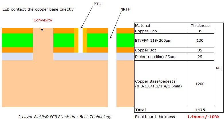
The 2 Layers SinkPAD board consists of two layers of trace circuit on same side, a dielectric (non-conducting) layer, a metal core/pedestal which normally is copper. As there’re two layers of trace circuits, so engineer can put more traces into the circuit on the same size circuit and then design more complicated board than 1 Layer SinkPAD board.
As the two layers of circuit traces are only on the top side if SinkPAD board too, so it’s also belonging to single sided SinkPAD PCB, and thermal PAD of LED will be put directly on copper core, also belonging to Direct Thermal Path (DTP) board too, so similar with 1L SinkPAD PCB, most of them are used in thermoelectric separation application too.
The SinkPad board provides excellent heat transfer from the LED to the base metal (copper) plate, while maintaining excellent electrical isolation. The base copper base gives the single-sided substrate mechanical integrity, distributes and transfers the heat to a heat sink, mounting surface or directly to the ambient air.
The 2 Layers copper base SinkPad PCB can be used with surface mount and chip & wire components, and provides much lower thermal resistance than normal MCPCB. As the thermal PAD of LED is touching the convexity of copper core/pedestal directly, so that thermal conductivity can be 400W/m.K, the same as the value of copper.
It is generally used for high power LED, the pad of LED touch the copper base directly, so that the heat generated by LED will be dissipated quickly into the air, or heatsink, which can achieve the best heat dissipation and conduction.
Stack up of 2 Layer SinkPAD Board
Advantages of Utilizing 2 layers SinkPAD Board:
Application of 2L SinkPAD Board
| 2 Layer SinkaPAD Board Capability | |
|
|
Click here to see the manufacturing process of 2 layers SinkPAD Board and other options.
If you want to customize 2 layer of SinkPAD board, please contact EBest Circuit (Best Technology) today send your request for SinkPAD Board.
ISimply drop your email or phone number in the contact form, and we'll promptly provide you with a quotation.