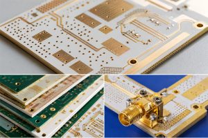
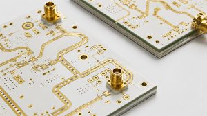
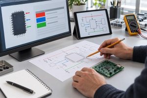
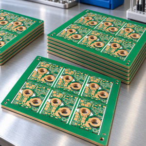
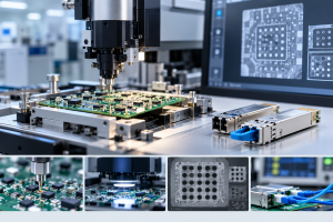
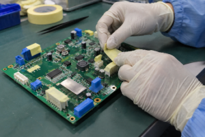
High-frequency PCB manufacturers in Europe cover PTFE multilayers, RF/FR-4 hybrid stackups, HDI, controlled impedance, 24–77 GHz radar PCBs, metal-backed boards, and RF testing. This guide compares seven manufacturers with documented European production and published high-frequency PCB capabilities.

Top 7 High-Frequency PCB Manufacturers in Europe
The seven manufacturers below differ mainly in RF material experience, layer structure, mmWave capability, HDI processing, production location, lead time, and target applications. The table provides a direct comparison of their published manufacturing strengths.
| Manufacturer | Manufacturing Site | Process Capability | Lead Time | Strength |
|---|---|---|---|---|
| ACB | France | PTFE, microwave laminates, multilayer RF PCB | Quick-turn available; by quote | RF and microwave PCB specialization |
| Aspocomp | Oulu, Finland | PTFE, RF/FR-4 hybrid, HDI, microvias, via filling | 3–20 days | RF + HDI integration |
| AT&S | Fehring, Austria | High-frequency PCB up to 10 layers, multilayer, HDI | By quote | Advanced multilayer capability and broad certifications |
| Eurocircuits | Europe | Rogers 4000 series, I-Tera, 2- and 4-layer RF PCB | 5 days bare / 10 days assembled for eligible RF Pool orders | Fast RF prototyping |
| KSG | Germany, Austria | 24–77 GHz, 2–20 layers, PTFE, hydrocarbon, hybrid multilayer | By quote | mmWave and radar PCB manufacturing |
| Schweizer Electronic | Schramberg, Germany | 6–24 GHz, 77 GHz, hybrid stackups, blind/buried vias | By quote | Automotive radar and sensor PCB |
| Teledyne Labtech | United Kingdom | PTFE, LCP, mixed dielectric, metal-backed PCB, blind/buried vias | From 5 days for qualifying prototypes | Complex RF/microwave PCB and RF testing |
What High-Frequency PCB Capabilities Do European Manufacturers Offer?
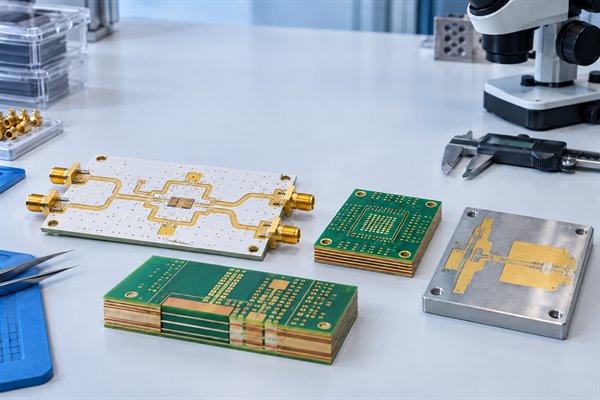
European manufacturers cover both conventional microwave PCBs and more complex structures that combine RF materials, multilayer construction, HDI, fine conductor control, thermal management, and mmWave processing. The following capabilities are the most relevant when comparing factories.
| Process | Capability |
|---|---|
| RF Laminates | PTFE, Rogers, I-Tera, hydrocarbon, LCP, mixed dielectric |
| Layer Count | 2-layer RF PCB to 20-layer multilayer PCB |
| Hybrid Stackups | RF laminate + FR-4 |
| HDI | Microvias, blind vias, buried vias, stacked and staggered vias |
| Controlled Impedance | Controlled-impedance transmission lines and verification |
| Fine-Line Etching | Published tolerances down to ±15 µm for selected processes |
| mmWave PCB | 24 GHz and 77 GHz radar and sensor PCB production |
| Via Processing | Via filling, copper-filled vias, via-in-pad |
| Special Structures | Metal-backed PCB, cavities, controlled-depth features |
| Assembly | SMT and RF PCB assembly |
| Testing | Electrical test, impedance verification, RF/microwave test |
At higher frequencies, trace width, dielectric thickness, copper profile, registration, and material stability have greater influence on impedance and insertion loss. For hybrid RF/FR-4 multilayers, lamination and dimensional compensation also become critical process controls.
Which Certifications Matter When Choosing a High-Frequency PCB Manufacturer in Europe?
Certifications should be matched to the application, production site, and required quality system. They are particularly relevant for automotive, aerospace, medical, and other regulated electronics.
- ISO 9001 — quality management system for general PCB manufacturing.
- IATF 16949 — relevant to automotive radar, ADAS, vehicle sensing, and automotive communication electronics.
- EN 9100 / AS9100 — used for aerospace and aviation electronics where traceability and process control requirements are higher.
- ISO 13485 — relevant to PCB production for medical devices and medical electronics.
- NADCAP — applies to qualified special processes in aerospace supply chains where required.
- ISO 14001 — covers environmental management systems.
- IPC-6018 — covers performance requirements for high-frequency and microwave printed boards.
Before supplier approval, verify the certificate holder, factory address, certification scope, and validity period against the site that will manufacture the PCB.
How Does Lead Time Differ Among European High-Frequency PCB Manufacturers?
High-frequency PCB lead time varies with RF material availability, PCB structure, lamination cycles, HDI processing, special mechanical features, testing, and assembly. Published quick-turn times normally apply only to designs that fit a defined process window.
| Manufacturer | Lead Time | Scope |
|---|---|---|
| ACB | Quick-turn available | Project-specific RF build |
| Aspocomp | 3–20 days | Oulu production |
| AT&S | By quote | Site and construction dependent |
| Eurocircuits | 5 days bare / 10 days assembled | Eligible RF Pool orders |
| KSG | By quote | Material and PCB structure dependent |
| Schweizer Electronic | By quote | Project-specific RF production |
| Teledyne Labtech | From 5 days | Qualifying prototypes |
Lead time usually increases with:
- special-order RF laminates
- high layer count
- PTFE or mixed-dielectric lamination
- sequential lamination
- microvias and filled vias
- cavities or controlled-depth routing
- metal-backed structures
- additional impedance or RF testing
- PCB assembly
For supplier comparison, use the required delivery date, not fabrication days alone. Material procurement, inspection, assembly, freight, and customs can materially change the final schedule.
How Does European High-Frequency PCB Manufacturing Compare With Asian Manufacturing?
For most sourcing decisions, the practical comparison is quality control, lead time, cost, process capability, material availability, engineering support, and production capacity. These factors affect both prototype development and volume production.
| Factor | European Manufacturing | Asian Manufacturing |
|---|---|---|
| Quality Control | Strong specialist RF factories and sector-specific quality systems | Established RF factories can support tight impedance, HDI, and high-reliability production |
| Lead Time | Shorter transport for European deliveries | Fast fabrication possible; international freight and customs add time |
| Cost | Higher labor and manufacturing overhead | Generally more competitive for medium- and high-volume production |
| Process Capability | Strong in specialty RF, radar, aerospace, and complex prototypes | Broad capability across RF, HDI, multilayer, hybrid, rigid-flex, and volume production |
| RF Materials | Strong specialist laminate experience | Broad material sourcing network and supplier base |
| Prototype Support | Strong regional quick-turn options | Competitive prototype fabrication with longer logistics to Europe |
| Volume Capacity | Some suppliers focus on specialty or lower-volume programs | Stronger large-volume manufacturing capacity |
| Engineering Support | Easier time-zone alignment for European programs | Depends on supplier engineering resources and response process |
| Production Origin | Suitable where European manufacture is required | Suitable where offshore manufacturing is accepted |
| Total Cost | Higher manufacturing cost but shorter regional logistics | Lower production cost; freight, customs, and inventory must be included |
European production is more suitable when local origin, regional engineering access, specialist RF processing, or shorter European logistics are required. Asian production is often stronger when volume capacity and manufacturing cost are higher priorities.
How Should You Choose the Right High-Frequency PCB Manufacturer in Europe?
The supplier should be evaluated against the actual RF stackup and the processes that are hardest to control on the board. A useful qualification compares measurable manufacturing capability rather than general claims such as “RF PCB supported.”
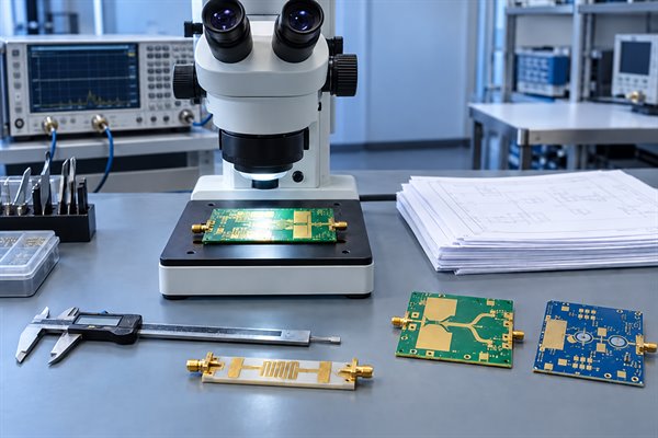
- Match the manufacturer to the operating frequency. A manufacturer experienced with a 2–6 GHz communication board is not automatically qualified for a 24 GHz or 77 GHz radar PCB. Check whether the factory has documented production experience near the required frequency range and with similar transmission-line structures.
- Confirm the exact RF material system. Specify the complete laminate grade rather than writing only “Rogers PCB” or “PTFE PCB.” Verify the core, prepreg or bonding material, dielectric thickness, copper type, material availability, and approved alternatives.
- Review the proposed stackup before releasing production files. For RF/FR-4 hybrid multilayers, confirm layer order, dielectric thickness, finished copper, impedance targets, lamination sequence, and material compatibility. Any stackup change can alter trace dimensions and impedance.
- Check the processes that affect RF performance. The most relevant controls include etching tolerance, conductor width, copper profile, dielectric thickness, registration, lamination, controlled-depth machining, and surface finish. For mmWave designs, small dimensional changes can have a measurable electrical effect.
- Verify HDI and via capability where required. For dense RF/digital boards, check microvia diameter, blind and buried vias, via-in-pad, copper filling, stacked or staggered vias, and sequential lamination. Confirm that these processes are qualified with the selected RF laminate rather than only standard FR-4.
- Confirm impedance control and inspection methods. Define the required impedance and tolerance on the fabrication drawing. Ask whether verification includes impedance coupons, TDR results, microsections, dimensional inspection, or other project-specific records.
- Check special RF and thermal structures. For high-power amplifiers, radar modules, antennas, or microwave systems, verify capability for metal-backed PCBs, cavities, thermal vias, copper-filled vias, controlled-depth routing, edge plating, or other required structures.
- Match certifications to the final application. A standard industrial RF PCB may require ISO 9001, while automotive radar may require IATF 16949 and aerospace electronics may require EN 9100/AS9100 or additional process approvals. Confirm that the certificate covers the actual production site.
- Compare lead time using the same starting point. Ask each manufacturer to quote from engineering approval and material availability through fabrication, inspection, assembly, and dispatch. This avoids comparing a five-day fabrication cycle with another supplier's complete delivery schedule.
- Check prototype and production capacity separately. A supplier may be excellent at prototypes but have limited volume capacity. Confirm prototype quantity, monthly production demand, panel requirements, expected ramp-up, and whether the same factory and process will be used after qualification.
- Confirm the manufacturing location. For PCB groups with plants in several countries, specify the required production site if country of origin, certification scope, logistics, or customer approval depends on it.
- Qualify the supplier with a representative build. The first build should contain the same RF laminate, stackup, critical conductor geometry, via structures, surface finish, and special processes planned for production. Review the finished PCB together with the agreed inspection records before approving volume production.
A strong supplier comparison should therefore answer five practical questions: Can the factory process the required RF material? Can it hold the critical geometry and impedance? Can it manufacture the full stackup and via structure? Can it provide the required quality evidence? Can it repeat the same process at the required production volume?
What Information Should You Provide When Requesting a High-Frequency PCB Quote?
A complete RFQ allows the manufacturer to review material availability, stackup feasibility, impedance, special processes, inspection requirements, and lead time before quotation. This reduces engineering questions after the order is released.
For PCB fabrication, provide:
- Gerber X2 or ODB++
- NC drill files
- fabrication drawing
- PCB dimensions
- layer count
- stackup
- RF laminate grade
- dielectric thickness
- copper thickness
- controlled impedance
- critical RF traces
- surface finish
- via structure
- finished hole size
- cavity or controlled-depth requirements
- metal-backed or thermal structures
- order quantity
- PCB acceptance standard
- test requirements
- delivery destination
For PCB assembly, also provide:
- BOM
- pick-and-place file
- assembly drawing
- approved substitutions
- programming requirements
- functional test requirements
- RF test requirements
If the stackup has not been finalized, complete the manufacturer stackup review before fixing the final RF trace width and spacing.
FAQs About High-Frequency PCB Manufacturers in Europe
The following questions cover common issues that arise when comparing European RF PCB suppliers, especially for Rogers materials, 77 GHz boards, hybrid stackups, HDI, lead time, and certification.
Q1: Are there Rogers PCB manufacturers in Europe?
A1: Yes. European manufacturers including ACB and Eurocircuits publish support for Rogers high-frequency laminate systems.
Q2: Which European manufacturers can produce 77 GHz PCBs?
A2: KSG and Schweizer Electronic publish 77 GHz PCB manufacturing capability, particularly for radar and sensing applications.
Q3: Can European manufacturers produce RF/FR-4 hybrid PCBs?
A3: Yes. Several manufacturers support mixed-dielectric multilayers combining RF laminates with FR-4.
Q4: Can high-frequency PCBs use HDI technology?
A4: Yes. Microvias, blind vias, buried vias, via-in-pad, and sequential buildup can be combined with RF structures when the material and process are qualified together.
Q5: Are European high-frequency PCB manufacturers faster than Asian suppliers?
A5: European production can reduce shipping time within Europe, while Asian factories may offer similar or shorter fabrication cycles. Compare total delivery time rather than fabrication time alone.
Q6: Are European high-frequency PCBs more expensive?
A6: European production generally has higher labor and manufacturing costs. Asian manufacturing is often more competitive for medium- and high-volume production.
Q7: Can European suppliers provide RF PCB assembly?
A7: Yes. Some manufacturers focus on bare PCB fabrication, while others provide PCB assembly and RF or microwave testing.
Q8: What process controls matter most for 77 GHz PCBs?
A8: Conductor geometry, dielectric thickness, copper profile, registration, impedance, and material stability become increasingly sensitive at mmWave frequencies.
Q9: Does ISO 9001 prove high-frequency PCB capability?
A9: No. ISO 9001 verifies the quality management system. RF capability must be evaluated through materials, process tolerances, impedance control, and testing.
Q10: Should the production site be confirmed before ordering?
A10: Yes. Confirm the actual manufacturing site whenever country of origin, certification scope, qualification, or logistics requirements apply.
Conclusion
KSG and Schweizer Electronic publish strong 77 GHz radar capability, Aspocomp combines RF materials with HDI, Eurocircuits provides standardized quick-turn RF prototypes, and Teledyne Labtech combines complex microwave PCB fabrication with RF testing.
If European manufacturing is not required, EBest Circuit provides custom high-frequency PCB fabrication and PCBA support from China, from prototype through volume production. We support custom stackups and free DFM review. Send your Gerber or ODB++, stackup, RF material, impedance requirements, quantities, BOM, and assembly files to sales@bestpcbs.com.