PCB manufacturing PCB manufacturing
Home > Blog

Microwave PCB

Top 7 High-Frequency PCB Manufacturers in Europe
Thursday, September 10th, 2026

High-frequency PCB manufacturers in Europe cover PTFE multilayers, RF/FR-4 hybrid stackups, HDI, controlled impedance, 24–77 GHz radar PCBs, metal-backed boards, and RF testing. This guide compares seven manufacturers with documented European production and published high-frequency PCB capabilities.

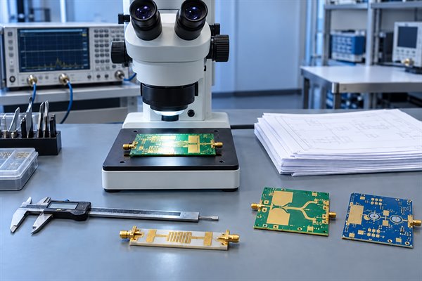
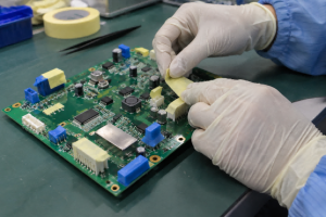
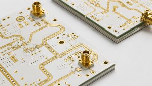
high-frequency PCB manufacturers in Europe, RF PCB samples in a precision electronics laboratory

Top 7 High-Frequency PCB Manufacturers in Europe

The seven manufacturers below differ mainly in RF material experience, layer structure, mmWave capability, HDI processing, production location, lead time, and target applications. The table provides a direct comparison of their published manufacturing strengths.

Manufacturer Manufacturing Site Process Capability Lead Time Strength
ACB France PTFE, microwave laminates, multilayer RF PCB Quick-turn available; by quote RF and microwave PCB specialization
Aspocomp Oulu, Finland PTFE, RF/FR-4 hybrid, HDI, microvias, via filling 3–20 days RF + HDI integration
AT&S Fehring, Austria High-frequency PCB up to 10 layers, multilayer, HDI By quote Advanced multilayer capability and broad certifications
Eurocircuits Europe Rogers 4000 series, I-Tera, 2- and 4-layer RF PCB 5 days bare / 10 days assembled for eligible RF Pool orders Fast RF prototyping
KSG Germany, Austria 24–77 GHz, 2–20 layers, PTFE, hydrocarbon, hybrid multilayer By quote mmWave and radar PCB manufacturing
Schweizer Electronic Schramberg, Germany 6–24 GHz, 77 GHz, hybrid stackups, blind/buried vias By quote Automotive radar and sensor PCB
Teledyne Labtech United Kingdom PTFE, LCP, mixed dielectric, metal-backed PCB, blind/buried vias From 5 days for qualifying prototypes Complex RF/microwave PCB and RF testing

What High-Frequency PCB Capabilities Do European Manufacturers Offer?

European manufacturers cover both conventional microwave PCBs and more complex structures that combine RF materials, multilayer construction, HDI, fine conductor control, thermal management, and mmWave processing. The following capabilities are the most relevant when comparing factories.
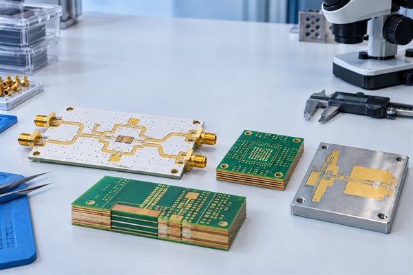
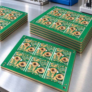
high-frequency PCB manufacturers in Europe, RF laminate and hybrid multilayer capability examples
Process Capability
RF Laminates PTFE, Rogers, I-Tera, hydrocarbon, LCP, mixed dielectric
Layer Count 2-layer RF PCB to 20-layer multilayer PCB
Hybrid Stackups RF laminate + FR-4
HDI Microvias, blind vias, buried vias, stacked and staggered vias
Controlled Impedance Controlled-impedance transmission lines and verification
Fine-Line Etching Published tolerances down to ±15 µm for selected processes
mmWave PCB 24 GHz and 77 GHz radar and sensor PCB production
Via Processing Via filling, copper-filled vias, via-in-pad
Special Structures Metal-backed PCB, cavities, controlled-depth features
Assembly SMT and RF PCB assembly
Testing Electrical test, impedance verification, RF/microwave test

At higher frequencies, trace width, dielectric thickness, copper profile, registration, and material stability have greater influence on impedance and insertion loss. For hybrid RF/FR-4 multilayers, lamination and dimensional compensation also become critical process controls.

Which Certifications Matter When Choosing a High-Frequency PCB Manufacturer in Europe?

Certifications should be matched to the application, production site, and required quality system. They are particularly relevant for automotive, aerospace, medical, and other regulated electronics.

  • ISO 9001 — quality management system for general PCB manufacturing.
  • IATF 16949 — relevant to automotive radar, ADAS, vehicle sensing, and automotive communication electronics.
  • EN 9100 / AS9100 — used for aerospace and aviation electronics where traceability and process control requirements are higher.
  • ISO 13485 — relevant to PCB production for medical devices and medical electronics.
  • NADCAP — applies to qualified special processes in aerospace supply chains where required.
  • ISO 14001 — covers environmental management systems.
  • IPC-6018 — covers performance requirements for high-frequency and microwave printed boards.

Before supplier approval, verify the certificate holder, factory address, certification scope, and validity period against the site that will manufacture the PCB.

How Does Lead Time Differ Among European High-Frequency PCB Manufacturers?

High-frequency PCB lead time varies with RF material availability, PCB structure, lamination cycles, HDI processing, special mechanical features, testing, and assembly. Published quick-turn times normally apply only to designs that fit a defined process window.

Manufacturer Lead Time Scope
ACB Quick-turn available Project-specific RF build
Aspocomp 3–20 days Oulu production
AT&S By quote Site and construction dependent
Eurocircuits 5 days bare / 10 days assembled Eligible RF Pool orders
KSG By quote Material and PCB structure dependent
Schweizer Electronic By quote Project-specific RF production
Teledyne Labtech From 5 days Qualifying prototypes

Lead time usually increases with:

  • special-order RF laminates
  • high layer count
  • PTFE or mixed-dielectric lamination
  • sequential lamination
  • microvias and filled vias
  • cavities or controlled-depth routing
  • metal-backed structures
  • additional impedance or RF testing
  • PCB assembly

For supplier comparison, use the required delivery date, not fabrication days alone. Material procurement, inspection, assembly, freight, and customs can materially change the final schedule.

How Does European High-Frequency PCB Manufacturing Compare With Asian Manufacturing?

For most sourcing decisions, the practical comparison is quality control, lead time, cost, process capability, material availability, engineering support, and production capacity. These factors affect both prototype development and volume production.

Factor European Manufacturing Asian Manufacturing
Quality Control Strong specialist RF factories and sector-specific quality systems Established RF factories can support tight impedance, HDI, and high-reliability production
Lead Time Shorter transport for European deliveries Fast fabrication possible; international freight and customs add time
Cost Higher labor and manufacturing overhead Generally more competitive for medium- and high-volume production
Process Capability Strong in specialty RF, radar, aerospace, and complex prototypes Broad capability across RF, HDI, multilayer, hybrid, rigid-flex, and volume production
RF Materials Strong specialist laminate experience Broad material sourcing network and supplier base
Prototype Support Strong regional quick-turn options Competitive prototype fabrication with longer logistics to Europe
Volume Capacity Some suppliers focus on specialty or lower-volume programs Stronger large-volume manufacturing capacity
Engineering Support Easier time-zone alignment for European programs Depends on supplier engineering resources and response process
Production Origin Suitable where European manufacture is required Suitable where offshore manufacturing is accepted
Total Cost Higher manufacturing cost but shorter regional logistics Lower production cost; freight, customs, and inventory must be included

European production is more suitable when local origin, regional engineering access, specialist RF processing, or shorter European logistics are required. Asian production is often stronger when volume capacity and manufacturing cost are higher priorities.

How Should You Choose the Right High-Frequency PCB Manufacturer in Europe?

The supplier should be evaluated against the actual RF stackup and the processes that are hardest to control on the board. A useful qualification compares measurable manufacturing capability rather than general claims such as ā€œRF PCB supported.ā€

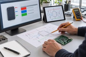
high-frequency PCB manufacturers in Europe, RF PCB inspection and supplier qualification
  1. Match the manufacturer to the operating frequency. A manufacturer experienced with a 2–6 GHz communication board is not automatically qualified for a 24 GHz or 77 GHz radar PCB. Check whether the factory has documented production experience near the required frequency range and with similar transmission-line structures.
  2. Confirm the exact RF material system. Specify the complete laminate grade rather than writing only ā€œRogers PCBā€ or ā€œPTFE PCB.ā€ Verify the core, prepreg or bonding material, dielectric thickness, copper type, material availability, and approved alternatives.
  3. Review the proposed stackup before releasing production files. For RF/FR-4 hybrid multilayers, confirm layer order, dielectric thickness, finished copper, impedance targets, lamination sequence, and material compatibility. Any stackup change can alter trace dimensions and impedance.
  4. Check the processes that affect RF performance. The most relevant controls include etching tolerance, conductor width, copper profile, dielectric thickness, registration, lamination, controlled-depth machining, and surface finish. For mmWave designs, small dimensional changes can have a measurable electrical effect.
  5. Verify HDI and via capability where required. For dense RF/digital boards, check microvia diameter, blind and buried vias, via-in-pad, copper filling, stacked or staggered vias, and sequential lamination. Confirm that these processes are qualified with the selected RF laminate rather than only standard FR-4.
  6. Confirm impedance control and inspection methods. Define the required impedance and tolerance on the fabrication drawing. Ask whether verification includes impedance coupons, TDR results, microsections, dimensional inspection, or other project-specific records.
  7. Check special RF and thermal structures. For high-power amplifiers, radar modules, antennas, or microwave systems, verify capability for metal-backed PCBs, cavities, thermal vias, copper-filled vias, controlled-depth routing, edge plating, or other required structures.
  8. Match certifications to the final application. A standard industrial RF PCB may require ISO 9001, while automotive radar may require IATF 16949 and aerospace electronics may require EN 9100/AS9100 or additional process approvals. Confirm that the certificate covers the actual production site.
  9. Compare lead time using the same starting point. Ask each manufacturer to quote from engineering approval and material availability through fabrication, inspection, assembly, and dispatch. This avoids comparing a five-day fabrication cycle with another supplier's complete delivery schedule.
  10. Check prototype and production capacity separately. A supplier may be excellent at prototypes but have limited volume capacity. Confirm prototype quantity, monthly production demand, panel requirements, expected ramp-up, and whether the same factory and process will be used after qualification.
  11. Confirm the manufacturing location. For PCB groups with plants in several countries, specify the required production site if country of origin, certification scope, logistics, or customer approval depends on it.
  12. Qualify the supplier with a representative build. The first build should contain the same RF laminate, stackup, critical conductor geometry, via structures, surface finish, and special processes planned for production. Review the finished PCB together with the agreed inspection records before approving volume production.

A strong supplier comparison should therefore answer five practical questions: Can the factory process the required RF material? Can it hold the critical geometry and impedance? Can it manufacture the full stackup and via structure? Can it provide the required quality evidence? Can it repeat the same process at the required production volume?

What Information Should You Provide When Requesting a High-Frequency PCB Quote?

A complete RFQ allows the manufacturer to review material availability, stackup feasibility, impedance, special processes, inspection requirements, and lead time before quotation. This reduces engineering questions after the order is released.

For PCB fabrication, provide:

  • Gerber X2 or ODB++
  • NC drill files
  • fabrication drawing
  • PCB dimensions
  • layer count
  • stackup
  • RF laminate grade
  • dielectric thickness
  • copper thickness
  • controlled impedance
  • critical RF traces
  • surface finish
  • via structure
  • finished hole size
  • cavity or controlled-depth requirements
  • metal-backed or thermal structures
  • order quantity
  • PCB acceptance standard
  • test requirements
  • delivery destination

For PCB assembly, also provide:

  • BOM
  • pick-and-place file
  • assembly drawing
  • approved substitutions
  • programming requirements
  • functional test requirements
  • RF test requirements

If the stackup has not been finalized, complete the manufacturer stackup review before fixing the final RF trace width and spacing.

FAQs About High-Frequency PCB Manufacturers in Europe

The following questions cover common issues that arise when comparing European RF PCB suppliers, especially for Rogers materials, 77 GHz boards, hybrid stackups, HDI, lead time, and certification.

Q1: Are there Rogers PCB manufacturers in Europe?

A1: Yes. European manufacturers including ACB and Eurocircuits publish support for Rogers high-frequency laminate systems.

Q2: Which European manufacturers can produce 77 GHz PCBs?

A2: KSG and Schweizer Electronic publish 77 GHz PCB manufacturing capability, particularly for radar and sensing applications.

Q3: Can European manufacturers produce RF/FR-4 hybrid PCBs?

A3: Yes. Several manufacturers support mixed-dielectric multilayers combining RF laminates with FR-4.

Q4: Can high-frequency PCBs use HDI technology?

A4: Yes. Microvias, blind vias, buried vias, via-in-pad, and sequential buildup can be combined with RF structures when the material and process are qualified together.

Q5: Are European high-frequency PCB manufacturers faster than Asian suppliers?

A5: European production can reduce shipping time within Europe, while Asian factories may offer similar or shorter fabrication cycles. Compare total delivery time rather than fabrication time alone.

Q6: Are European high-frequency PCBs more expensive?

A6: European production generally has higher labor and manufacturing costs. Asian manufacturing is often more competitive for medium- and high-volume production.

Q7: Can European suppliers provide RF PCB assembly?

A7: Yes. Some manufacturers focus on bare PCB fabrication, while others provide PCB assembly and RF or microwave testing.

Q8: What process controls matter most for 77 GHz PCBs?

A8: Conductor geometry, dielectric thickness, copper profile, registration, impedance, and material stability become increasingly sensitive at mmWave frequencies.

Q9: Does ISO 9001 prove high-frequency PCB capability?

A9: No. ISO 9001 verifies the quality management system. RF capability must be evaluated through materials, process tolerances, impedance control, and testing.

Q10: Should the production site be confirmed before ordering?

A10: Yes. Confirm the actual manufacturing site whenever country of origin, certification scope, qualification, or logistics requirements apply.

Conclusion

KSG and Schweizer Electronic publish strong 77 GHz radar capability, Aspocomp combines RF materials with HDI, Eurocircuits provides standardized quick-turn RF prototypes, and Teledyne Labtech combines complex microwave PCB fabrication with RF testing.

If European manufacturing is not required, EBest Circuit provides custom high-frequency PCB fabrication and PCBA support from China, from prototype through volume production. We support custom stackups and free DFM review. Send your Gerber or ODB++, stackup, RF material, impedance requirements, quantities, BOM, and assembly files to sales@bestpcbs.com.
You may also like

Common Microwave PCB FAQs, RF Microwave PCB Solutions
Wednesday, December 3rd, 2025

Microwave PCBs are the foundation of today’s radar sensors, satellite communication modules, 5G mmWave devices, and high-frequency RF front-end systems. Operating between 300 MHz and 300 GHz, microwave circuits require extremely low signal loss, minimal phase distortion, and precise impedance control. Because of these challenges, engineers and buyers often have many questions when choosing materials, designing stack-ups, or selecting a reliable microwave PCB manufacturer.

This article compiles the common Microwave PCB FAQs, covering materials, stack-ups, design rules, testing, troubleshooting, and how to choose a UL/CE certified microwave PCB manufacturer. Let’s dive in.

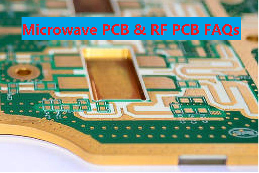
Common Microwave PCB FAQs, RF Microwave PCB Solutions

1. What is the difference between RF PCB and microwave PCB?

RF PCBs typically operate below 6 GHz, while microwave PCBs are engineered for 6–100+ GHz applications. Microwave boards require lower-loss materials, tighter impedance control, and more precise manufacturing.

2. Can FR4 be used for microwave PCBs?

Generally no. FR4 has high dielectric loss (Df) and unstable Dk at high frequencies, causing significant signal degradation above ~3–4 GHz. Microwave designs typically use PTFE, ceramic-filled PTFE, hydrocarbon ceramics, or hybrid stackups.

3. What materials are best for microwave PCBs?

Common high-performance materials include:

  • Rogers RO4003C / RO4350B
  • Rogers RT/duroid 5880, 6002, 6035HTC
  • Taconic TLY, RF-35
  • Arlon CLTE-XT, IsoClad
  • Hybrid FR4 + Rogers constructions

These materials provide low loss, stable dielectric constants, and excellent high-frequency performance.

4. Why is impedance control critical for microwave circuits?

At microwave frequencies, PCB traces behave like transmission lines. Even a 5–10% impedance error can cause:

  • Higher insertion loss
  • Return loss and reflection
  • Phase distortion
  • Reduced antenna efficiency

Therefore, maintaining a precise 50Ī© or 75Ī© impedance is mandatory.

5. What is a grounded coplanar waveguide (GCPW) and why is it used?

GCPW is a transmission line structure where the RF trace is flanked by ground on both sides with a ground plane below.

It is preferred for microwave PCBs because it offers:

  • Excellent isolation
  • Consistent impedance
  • Low radiation loss
  • Compact routing for dense layouts

This makes it ideal for RF microwave PCB solutions in 5G and radar applications.

6. Do microwave PCBs require special surface finishes?

Yes. Surface finishes impact insertion loss and skin effect at GHz frequencies.

Recommended finishes:

  • Immersion Silver (IAg) → lowest loss
  • ENEPIG → stable & reliable for wire bonding
  • ENIG → commonly used but slightly higher loss

Avoid heavy plating thicknesses that increase skin resistance.

7. Does the thickness of a microwave PCB affect performance?

Absolutely. PCB thickness affects:

  • Impedance
  • Loss tangent
  • Coupling
  • Antenna bandwidth
  • Propagation delay

Thinner boards generally provide better high-frequency performance and smaller trace widths.

8. How small can a microwave PCB be?

Microwave PCBs can be extremely compact (millimeter scale), but size is often dictated by:

  • Antenna requirements
  • Transmission line spacing
  • Ground via placement
  • Heat management

For mmWave modules (24–80 GHz), PCBs are often less than 20 Ɨ 20 mm.

9. Can microwave PCBs support high power?

Some can, but it depends on the material.

Ceramic-filled PTFE laminates like RO3006/3010 support higher power due to:

  • Better thermal stability
  • Lower expansion
  • Higher breakdown voltage

Always calculate thermal dissipation for PA circuits.

10. How do you test a microwave PCB?

Common testing methods include:

  • Time Domain Reflectometry (TDR) – impedance
  • Vector Network Analyzer (VNA) – S-parameters
  • Insertion loss and return loss measurement
  • Phase stability tests
  • Thermal cycling / reliability testing

Certified manufacturers provide full RF test reports.

11. What causes failure in a microwave control board?

Typical failure points include:

  • Overheating of high-power components
  • Delamination of PTFE materials
  • Dielectric breakdown
  • Trace burns or micro-cracking
  • Faulty solder joints
  • Moisture absorption in high-frequency laminates

Environmental stress factors accelerate failures at GHz speeds.

12. How long does it take to manufacture a microwave PCB?

Lead times depend on stackup complexity:

  • Simple 2–4 layer microwave PCB: 7–10 days
  • Hybrid PTFE/FR4 stackups: 10–15 days
  • Advanced mmWave designs (20–80 GHz): 15–25 days

Prototype + testing may take longer.

13. Are microwave PCBs expensive?

Yes, they cost more than standard FR4 because materials like Rogers/PTFE have higher prices and require specialized equipment.

Cost is influenced by:

  • Material grade
  • Layer count
  • Precision machining
  • Tight impedance tolerance
  • Surface finish

Large-scale production reduces cost significantly.

14. How do I source microwave PCBs with UL/CE certification?

Choose a manufacturer that specializes in RF & microwave PCB solutions and provides:

  • UL-recognized laminates
  • CE-compliant process control
  • Rogers, Taconic, and Arlon material handling
  • Impedance test reports
  • Cleanroom lamination for hybrid constructions

15. Can microwave PCBs be multilayer?

Yes. Many microwave designs use 4–12 layer stackups, with PTFE or hydrocarbon layers sandwiched between FR4.

Common structures include:

  • PTFE outer layers + FR4 inner layers
  • Full PTFE stack for ultra-low-loss radar systems
  • PTFE + ceramic for mmWave phased arrays

16. What is the maximum frequency a PCB can support?

It depends on the laminate.

Typical limits:

  • FR-4: < 6 GHz (with losses)
  • Rogers 4000 series: ~20–40 GHz
  • PTFE-based materials: 40–110 GHz
  • Ceramic-filled materials: up to 110+ GHz and mmWave bands

For 5G, radar, and satellite systems, PTFE or ceramic laminates are recommended.

17. Do microwave PCBs require controlled dielectric thickness?

Yes. Dielectric thickness tolerance is critical because it directly affects:

  • Impedance accuracy
  • Coupling and isolation
  • Phase delay
  • Overall microwave matching performance

High-frequency PCB fabricators must maintain ±10% or even ±5% dielectric thickness tolerance for mission-critical use.

18. Why is copper roughness important in microwave PCBs?

At microwave and mmWave frequencies, skin depth becomes extremely small.
Rough copper dramatically increases:

  • Conductor loss
  • Insertion loss
  • Heating

Many designers specify rolled annealed (RA) copper or low-profile copper (VLP/LP) to keep losses under control.

19. Can microwave PCBs be made flexible (RF flex circuits)?

Yes—flexible microwave PCBs use materials like:

  • Rogers 3000 series flexible laminates
  • Polyimide-based low-Dk materials

Applications include antennas, phased arrays, and wearable radar sensors.

20. What is the expected lifetime of a microwave PCB?

With proper material selection and thermal design:

  • Consumer microwave PCBs: 5–10 years
  • Automotive radar PCBs: 10–15 years
  • Aerospace/military microwave PCBs: 20+ years

Failure is usually caused by thermal cycling, moisture absorption, or RF overstress.

21. How long does it take to manufacture microwave PCBs?

Typical lead times:

  • Standard microwave PCB: 10–15 days
  • Complex multilayer microwave PCB: 15–25 days
  • Hybrid stack-up with PTFE: 20–30 days

Fast-turn service (5–7 days) is possible but more expensive.

22. What Is the Typical Thickness of a Microwave PCB?

Dielectric layers:

  • 0.127 mm
  • 0.254 mm
  • 0.508 mm
  • 0.8 mm

Final PCB thickness:

0.4–1.6 mm depending on application.

23. What Are the Main Applications of Microwave PCBs?

Microwave PCBs are used in:

  • 24/60/77 GHz automotive radar
  • 5G mmWave radio units
  • Microwave antennas
  • Satellite transceivers
  • PA/LNA modules
  • RF filters and couplers
  • Medical microwave imaging
  • Wireless base stations
  • Military radar systems

Above are the common questions that we faced during working, if you have any other questions about microwave PCBs or radio frequency PCBs, just feel free to contact us.

You may also like

What is a Microwave PCB? An Ultimate Guide 2026
Wednesday, December 3rd, 2025

A microwave PCB handles signals that run at very high frequencies, and these boards support systems that need clean, stable performance. You will find a microwave PCB in equipment such as radar modules, satellite links, high-speed wireless platforms, and precision test devices. As industries push toward higher data rates and smaller RF systems, the need for dependable microwave boards grows quickly.

Today, many engineers search for rf microwave PCB options that keep loss low and impedance steady. Others look for complete rf & microwave PCB solutions that simplify material choice, stack-up planning, and manufacturing. If you’re evaluating RF microwave PCB materials or sourcing RF & microwave PCB solutions, this article will give you a complete understanding.

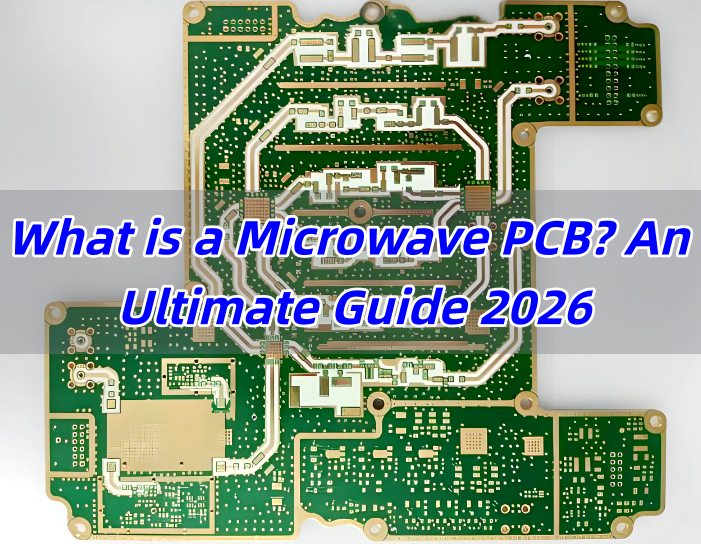
What is a Microwave PCB? An Ultimate Guide 2026

What Is a Microwave PCB?

A microwave PCB is a printed circuit board designed to operate at extremely high frequencies, typically:

  • Microwave band: 300 MHz – 30 GHz
  • Millimeter-wave (mmWave): 30 – 100+ GHz

At these frequencies, PCB traces behave like transmission lines, and even tiny layout variations can impact signal loss, phase accuracy, antenna performance, and overall system reliability.

Microwave PCBs are commonly used in radar systems, satellite communication, aerospace navigation, and 5G mmWave modules. Compared with standard RF boards, microwave PCBs demand more precise materials, controlled impedance, and stricter fabrication tolerances.

What Materials Are Used for Microwave PCBs?

Material choice is one of the most important decisions in microwave design. Standard FR-4 cannot support microwave frequencies due to high loss and unstable dielectric properties. Instead, microwave PCBs use advanced materials engineered for low loss and tight dielectric tolerances.

Here are the materials most commonly used:

Material TypeExamplesFeaturesBest Use Case
PTFE (Teflon)RT/duroid 5880, Taconic TLYExtremely low loss, stable Dk, best for high GHzRadar, mmWave, satellites
Hydrocarbon CeramicsRogers RO4350B, RO4003CLow loss, easy to manufacture, cost-effective1–20 GHz microwave circuits
Ceramic-Filled PTFERogers RO3006/3010Ultra-stable Dk, low thermal expansionHigh-power microwave and phased arrays
Hybrid StackupsFR4 + RogersPerformance + lower costMixed-signal RF/microwave designs

The best material depends on target frequency, environmental exposure, and mechanical requirements. Each laminate affects loss, phase stability, and long-term reliability.

Key Design Rules and Layout for Microwave PCB Design

Designing a microwave PCB is very different from routing a standard digital or low-frequency board. At microwave frequencies, each copper trace behaves like a transmission line. Small changes in width, dielectric height, copper roughness, or via structure can shift impedance and alter the entire RF chain. Because of that, layout and stack-up design must follow strict engineering rules to keep signal quality stable.

Key Design Rules and Layout for Microwave PCB Design

Below are the core principles used by RF engineers when building reliable microwave layouts.

1. Maintain Tight Impedance Control

Stable impedance is the foundation of microwave design. Even small dimensional changes can introduce reflections or distort the waveform.

Key requirements:

  • Define target impedance early (commonly 50Ī© or 75Ī©).
  • Choose the correct structure: microstrip, stripline, or grounded coplanar waveguide (GCPW).
  • Keep trace width consistent along the entire path.
  • Maintain stable dielectric thickness and copper thickness.
  • Use field-solver tools (ADS, HFSS, CST, Polar SI, or Altium impedance calculator).
  • Keep differential pairs phase-matched if used in RF mixers or high-frequency paths.

GCPW is widely used for microwave PCB design because it offers strong field confinement and supports compact layouts.

2. Use Smooth Routing Instead of Sharp Corners

High-frequency energy does not like sudden changes. Sharp corners cause impedance shifts and increase local reflections.

Preferred routing practices:

  • Avoid 90° turns.
  • Use gradual curves (arc routing) for cleaner field transitions.
  • Use mitered 45° bends if space is limited.
  • Keep sensitive paths straight and short whenever possible.

Smooth routing helps preserve phase stability and reduces insertion loss.

3. Keep the Ground Plane Continuous

A microwave signal needs a clean, uninterrupted return path. Gaps in the ground plane cause radiation, coupling, and impedance drift.

Ground plane guidelines:

  • Maintain a solid ground layer directly under RF traces.
  • Avoid splits, voids, or cutouts beneath the signal path.
  • Do not place digital return paths through RF areas.
  • Add stitching vias around RF traces to create a ā€œvia fenceā€ barrier.

A well-designed ground structure stabilizes the electromagnetic field and reduces unwanted emissions.

4. Manage Vias Carefully

A via is not just a hole at microwave frequencies—it’s a small inductor. Too much via inductance can degrade signal quality.

Best practices for vias:

  • Avoid unnecessary layer jumps.
  • Use multiple parallel vias to lower effective inductance.
  • Keep via barrels short when possible.
  • Add grounding vias around pads and connectors to improve shielding.
  • Avoid routing RF traces directly over via fields or ground voids.

Good via strategy can significantly improve stability in PA, LNA, and filter sections.

5. Select the Right Transmission Line Structure

Different RF paths require different structures depending on frequency, isolation, and mechanical constraints.

Common options:

  • Microstrip – simple, ideal for top-layer routing.
  • Stripline – fully shielded, good for noise-sensitive circuits.
  • Grounded coplanar waveguide (GCPW) – excellent isolation, compact layout, and easy impedance tuning.
  • Wide microstrip – lower conductor loss, suitable for power amplifiers.

GCPW has become the most popular for microwave work due to its predictable behavior and high routing density.

6. Align Components with the Signal Flow

Component orientation affects load matching and return loss.

Component placement guidelines:

  • Place RF blocks (filter, LNA, PA, mixer) in the order of the signal chain.
  • Keep matching networks close to device pins.
  • Avoid unnecessary gaps between RF parts.
  • Place RF connectors, such as SMA or SMP, near the board edge for clean transitions.

When Should You Choose Microwave PCB vs. RF PCB?

Many engineers compare microwave PCBs with standard RF boards because both handle high-frequency signals. But the decision depends on frequency, performance targets, and loss tolerance.

TechnologyFrequency RangeBest For
RF PCBUp to ~6 GHzBluetooth, Wi-Fi, sub-6 GHz communication
Microwave PCB6–100+ GHz5G mmWave, radar, satellite, high-precision sensing

Choose an RF PCB when:

  • Frequencies are below 6 GHz
  • Cost is a major concern
  • FR-4 or mixed-material stackups are acceptable

Choose a Microwave PCB when:

  • You operate above 6 GHz
  • You require ultra-low loss
  • Your system needs stable phase and predictable impedance
  • Applications involve radar, mmWave, or satellite links

In short, microwave PCBs suit high-precision projects where even small layout or material changes can affect real performance. They are the preferred choice for radar, satellite links, and advanced communications.

Microwave PCBs Applications & Industries

Microwave PCBs appear in many sectors because they support stable, low-loss transmission for sensitive circuits. You’ll often see them in systems that require fast data, long-range signal paths, or precise sensing.

Common applications include:

  • 5G and 6G wireless infrastructure
  • Satellite communication systems (SATCOM)
  • Automotive radar (24 GHz, 77 GHz)
  • Military and commercial radar platforms
  • Microwave filters, couplers, and antennas
  • High-frequency power amplifiers
  • Navigation and guidance systems
  • Medical imaging devices such as MRI coils
  • Instrumentation and RF test equipment
  • Industrial microwave heating and sensing

These industries rely on microwave boards because small performance shifts can affect overall system behavior. Stable materials and predictable routing keep these systems accurate and responsive.

Microwave PCBs Applications & Industries

Does Size of a Microwave PCB Affect Its Application?

Yes, board size can influence performance because microwave signals respond to physical dimensions. At these frequencies, even a few millimeters can change how energy travels.

Board size affects:

  • Impedance stability:Longer traces add more loss and potential phase distortion.
  • Resonance behavior:Larger boards can introduce unwanted resonances.
  • Shielding structure:Compact layouts may need tighter via fences.
  • Thermal changes:Bigger boards may expand more under heat, shifting dielectric spacing.
  • Antenna performance:Antenna length and board shape affect radiation patterns.

Small boards require sharper tolerance control. Large boards demand stronger handling of expansion and material stability. The ideal size depends on whether the circuit is an antenna, filter, amplifier, or sensor.

How to Tell If a Microwave Control Board Is Bad?

Many users ask this because microwave ovens and industrial microwave systems depend on small control boards. Failures are often easy to spot once you know what to check. Common signs of a bad microwave control board include:

  • No power, no response, or blank display
  • Buttons that fail to react
  • Burning smell or visible damage
  • Unusual noises or sparking
  • Microwave stops heating while lights and fan still work
  • Random behavior such as auto-starting or shutting off
  • Relays that click repeatedly without function

If above signs occur, you can perform below visual checks safely:

  • Scorch marks or dark spots
  • Swollen capacitors
  • Cracked solder joints
  • Damaged connectors
  • Loose ribbon cables

These symptoms point to circuitry or relay failure. For home microwaves, technicians often replace the entire board rather than repair individual components.

How Much Does It Cost to Repair a Microwave Circuit Board?

Repair cost depends on equipment type, part availability, and labor requirements.

Typical consumer microwave repair ranges:

  • Basic repair: USD 80–120
  • Control board replacement: USD 120–250
  • High-end or built-in models: USD 180–350

Industrial microwave equipment repair ranges:

  • Board-level component repair: USD 250–600
  • Full board replacement: USD 400–1,200+ depending on complexity

Factors that influence cost include:

  • Part scarcity
  • Board size and layer count
  • Number of relays, sensors, or high-voltage circuits
  • Whether the board is conformal-coated
  • Testing and calibration requirements

Consumer microwaves are often cheaper to replace than repair, but industrial microwave systems usually justify board-level repair. EBest Circuit (Best Technology) can repair the microwave circuit board for free if your PCB are ordered from our company.

Where to Get RF Microwave PCB Boards with UL/CE Certification?

Many companies need microwave PCBs that meet safety and compliance standards, especially when the final product enters global markets. UL and CE certifications help confirm material reliability and safety. When sourcing certified microwave boards, a good supplier should provide:

  • UL-certified laminates (Rogers, Taconic, Arlon, Panasonic)
  • CE-compliant production and testing
  • Rogers/PTFE/ceramic microwave PCB fabrication
  • Controlled impedance testing reports
  • Hybrid laminations and multi-layer microwave stackups
  • RF & microwave PCB solutions for 1–100 GHz

EBest Circuit (Best Technology) is a strong option for RF and microwave PCB production because the company offers:

  • UL-approved material systems
  • Stable performance with PTFE, Rogers, and ceramic-filled substrates
  • Tight impedance control for microwave designs
  • Complete CE-related documentation support
  • Strong engineering assistance during stack-up and DFM review
  • Consistent production with IPC standards
  • Fast global delivery for prototypes and batches

If you are preparing a new microwave PCB or RF hardware program, welcome to contact us at sales@bestpcbs.com, our team is 24/7 hours online for you!

You may also like