PCB manufacturing PCB manufacturing
Home > Blog

RF Amplifier PCB Design & Layout, Free DFM

December 3rd, 2025

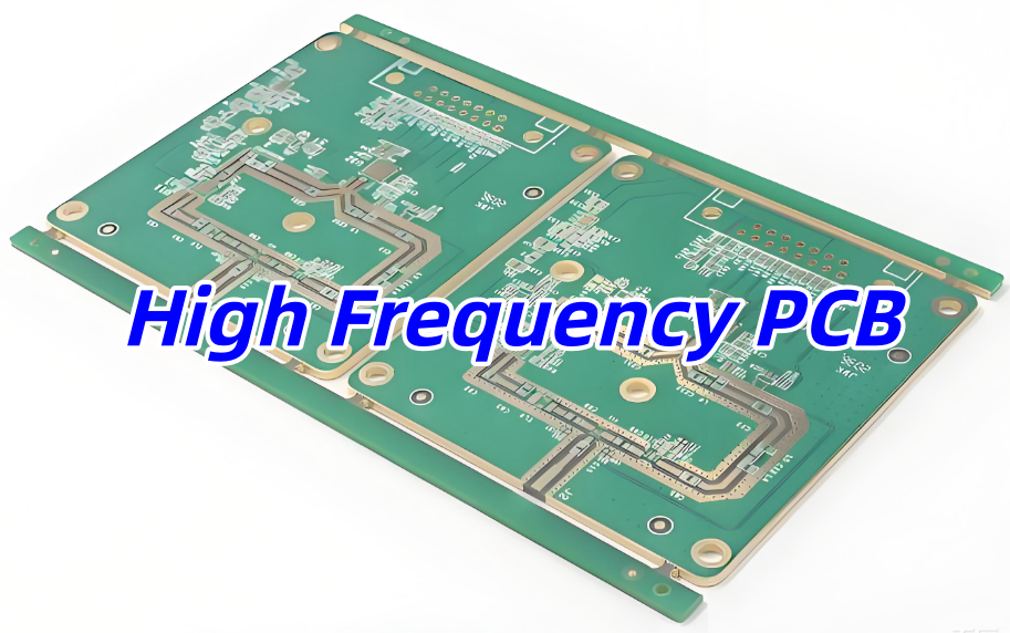
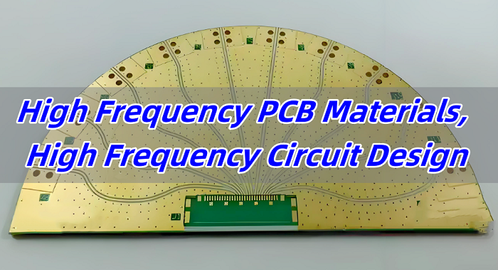
How to design a RF amplifier PCB? This blog covers types, applications, technical parameter, design guideline and layout technique for RF amplifier PCB.

Are you troubled with these questions?

  • How to ensure PCB stability and low noise amid RF signal interference?
  • How to quickly optimize high-frequency impedance matching to avoid performance loss?
  • How to maintain stable high-frequency performance in mass production?

As a RF amplifier PCB manufacturer, EBest Circuit (Best Technology) can provide you service and solutions:

  • Precise Simulation & Optimization: Leverage ANSYS HFSS for EM simulation, cutting design iterations by 2-3 cycles with 40% efficiency gain. Achieve <5% signal integrity error and <0.8dB noise figure.
  • Impedance Matching Expertise: 20+ years of experience ensures ±3% impedance control via material selection and stack-up design, boosting matching efficiency by 20% and reducing signal loss by 15%.
  • Quality Control & Rapid Response: Full-process monitoring and S-parameter/eye-diagram testing ensure batch-to-batch high-frequency parameter deviation <±1%. Samples in 7 days, mass production in 15 days, with 98% on-time delivery rate.

Welcome to contact us if you have any request for RF amplifier PCB design and assembly: sales@bestpcbs.com.

What Is A RF Amplifier PCB?

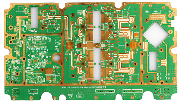
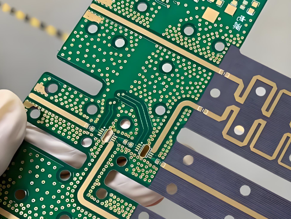
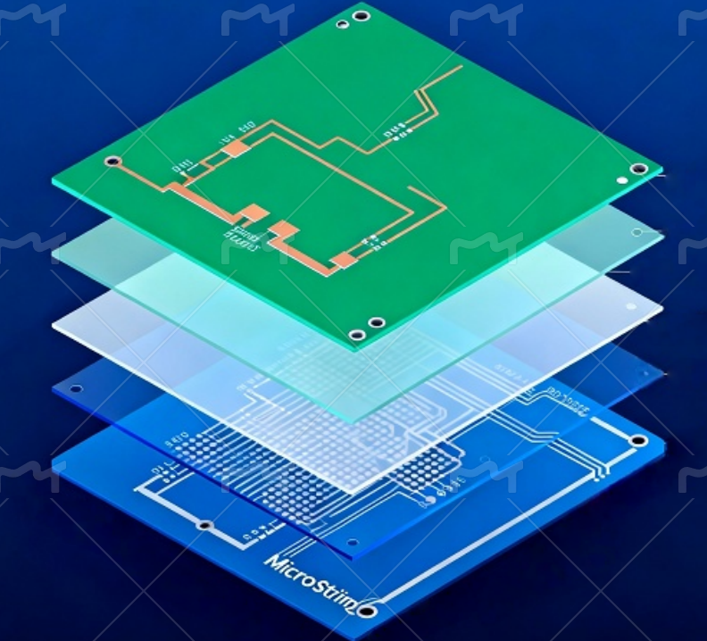
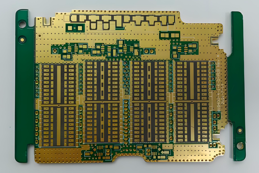
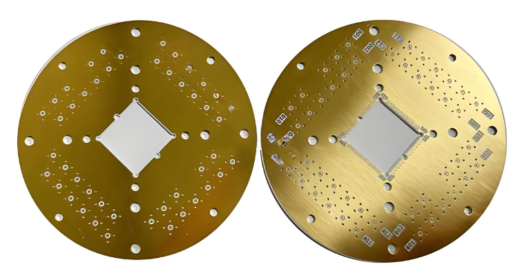
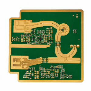
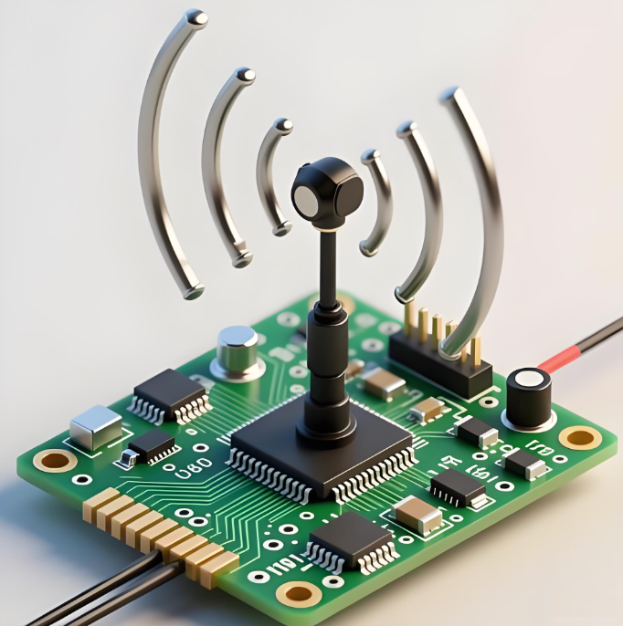
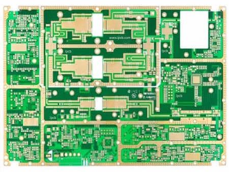
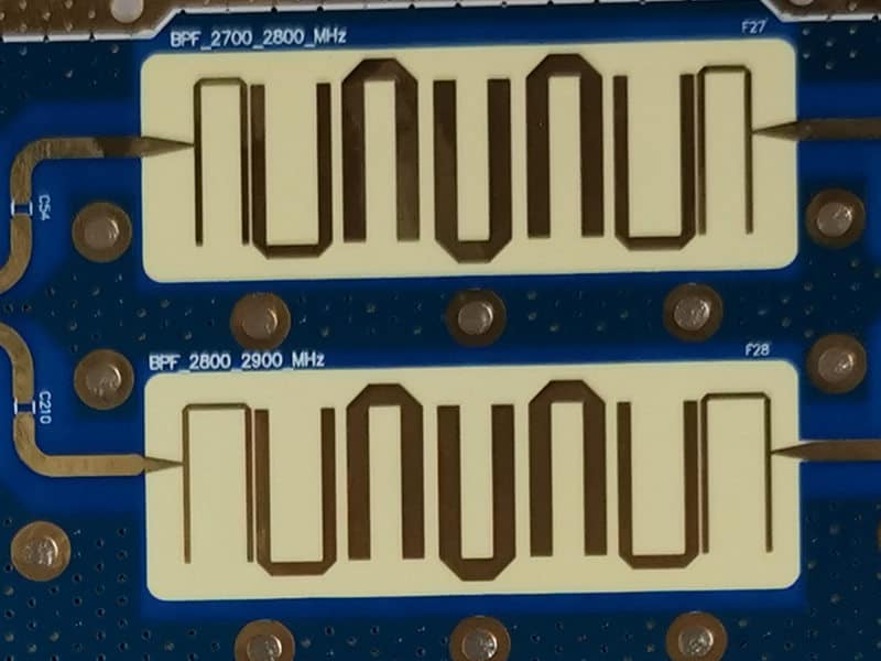
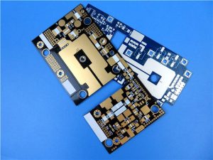
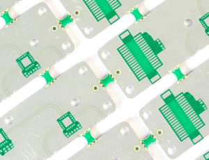
A RF amplifier PCB is a circuit board created to support amplification stages that work in radio-frequency ranges. It carries components such as low-noise amplifiers, gain blocks, filters, bias circuits, and matching networks. Since RF energy reacts to small layout changes, the board must control impedance, grounding, and routing with more care than general PCBs. Furthermore, material choice, stack-up, and copper patterns influence how signals move through each trace. When these factors align, the amplifier remains stable, gains remain predictable, and unwanted radiation stays low.

What Is A RF Amplifier PCB

What Are Types of RF Amplifier PCBs?

  • Low-Noise Amplifier (LNA) PCB: These boards serve front-end systems in radios, satellite receivers, and radar sensors. Their goal is to lift micro-level input signals with very low added noise. LNAs rely on controlled impedance, a short input path, and a clean ground to reduce noise figure.
  • Power Amplifier (PA) PCB: PA boards push RF energy to a much higher level. They appear in transmitters, cellular base stations, industrial heating systems, and radar emitters. Because of higher current, these boards need thick copper, thermal relief paths, and stable bias networks.
  • Driver Amplifier PCB: A driver board takes medium-level signals and prepares them for a PA stage. It must handle some power while still keeping reasonable linearity.
What Are Types of RF Amplifier PCBs?

What Are Applications of RF Amplifier PCB Board?

  • 5G, LTE, and Wi-Fi systems in mobile devices and base stations.
  • Radar sensors used in autonomous driving, drones, and traffic monitoring.
  • Satellite communications for navigation, broadcasting, and remote sensing.
  • IoT nodes that need compact front-end amplification.
  • Test and measurement devices such as spectrum analyzers and signal generators.
  • Medical imaging and diagnostic tools that involve RF detection stages.
  • Industrial RF heating and plasma equipment.

RF Amplifier PCB Design Technical Parameter

ParameterTypical Specification
Operating Frequency Range0.5–6 GHz
Gain20±1 dB @ 25°C
Noise Figure (NF)≤1.2 dB (LNA) / N/A (PA)
Output Power (Pout)30 dBm (PA) / 10 dBm (Driver)
Output Third-Order Intercept Point (OIP3)+40 dBm
Voltage Standing Wave Ratio (VSWR)≤1.5:1 (Input/Output)
Operating Voltage+5V DC, ±10%
Operating Current120 mA (LNA) / 800 mA (PA)
Power Added Efficiency (PAE)>45% (PA)
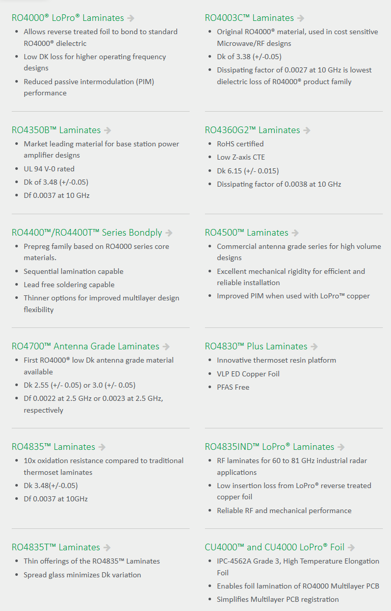
PCB SubstrateRogers 4350B/Taconic RF-35/FR4-HF
Copper Thickness1–2 oz (35–70 μm)
Impedance Control Accuracy50Ω ±5%
Layer Count2–8 layers
Thermal Resistance (θja)≤15°C/W (PA with Heatsink)
Operating Temperature-40℃ ~ +85℃
Storage Temperature-55℃ ~ +125℃
Humidity Tolerance95% Non-condensing
EMC StandardsFCC Part 15, CE, RoHS 3
Lead-free ProcessCompliant (Sn96.5/Ag3.0/Cu0.5)
Mean Time Between Failures (MTBF)>100,000 hours
I/O InterfacesSMA/QMA/MMCX/Solder Pads
Shielding EnclosureOptional EMI Shielding Case
Test PointsIntegrated VNA Calibration Test Points

RF Amplifier PCB Design Guideline

A detailed guideline to RF amplifier PCB design:

1. Layout Partitioning and Isolation Design

  • Mixed-signal isolation: Strictly separate analog, digital, and RF zones. Maintain minimum spacing of 10mm (≥20mm for high-frequency applications) between digital circuits and RF sections to prevent cross-coupling. Implement “star” power routing to minimize noise crosstalk. Position sensitive components (e.g., LNAs, mixers) close to antennas or RF ports to reduce path length and losses.
  • Shielding and grounding: Use via fences (spacing ≤λ/20) to construct isolation bands. Install metal shielding enclosures (e.g., copper cavities) in sensitive areas. Ensure continuous ground planes without segmentation. Recommend dual-layer grounding with via stitching (spacing ≤λ/10) to enhance EMI protection.

2. Impedance Control and Transmission Line Design

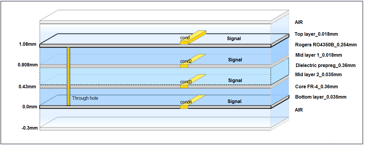
  • Material selection: For frequencies above 1GHz, prioritize low-loss substrates (e.g., Rogers RO4350B, Taconic RF-35) over traditional FR4 (loss tangent 0.02-0.025). Materials must meet stable dielectric constant (Dk: 3.48±0.05@10GHz) and low moisture absorption (<0.1%).
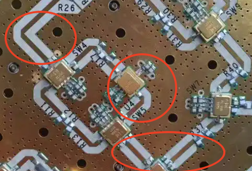
  • Impedance matching: Transmission line characteristic impedance must precisely match standards (e.g., 50Ω). Use microstrip/stripline structures and avoid 90° bends; adopt 45° miters or curved transitions. Validate stackup designs with field solvers (e.g., Polar Si8000) to maintain <±10% impedance tolerance.
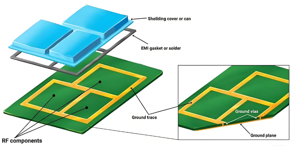
3. Power and Thermal Management

  • Decoupling and filtering: Deploy multi-stage filtering (LC/π networks) at power entry points. Place small-value (0.1μF) ceramic capacitors near ICs combined with bulk (10μF) electrolytic capacitors in “star” topology to reduce IR drops.
  • Thermal design: Under high-power devices (e.g., PAs), implement thermal via arrays filled with conductive adhesive. Integrate heat sinks or metal-core substrates (e.g., aluminum) to enhance heat dissipation, ensuring junction temperature remains below 125°C.

4. Signal Integrity and EMC Protection

  • Routing rules: Avoid cross-layer via transitions for RF signal lines. When necessary, use via-in-pad or back-drilling to eliminate stubs. Maintain ≥3× line width spacing between high-speed digital signals and RF traces, or employ differential pairs for balanced transmission.
  • EMI suppression: Install ground traces along board edges and common-mode chokes at critical interfaces. Optimize layouts through simulation (ADS/HFSS) and ensure compliance with FCC/CE radiation limits (e.g., EN55022).

5. Manufacturing and Testability Design

  • Process specifications: Adhere to IPC-6012 standards. Define minimum trace width/spacing compatible with manufacturing capabilities (e.g., 100μm for HDI processes). Specify stackup details including layer thickness, copper weight, and solder mask dimensions.
  • Test validation: Include test points (e.g., SMA connectors) and debugging pads. Deploy temperature rise monitoring at critical nodes. Verify S-parameters (e.g., S21, S11) with network analyzers to confirm gain and noise figure specifications.

6. Documentation and Regulatory Compliance

  • Design documentation: Provide complete BOM, Gerber files, stackup reports, and simulation models. Annotate critical parameters (Dk/Df values, thermal resistance curves) with international certifications (UL, RoHS).
  • Regulatory adaptation: Configure power filtering solutions to meet regional standards (e.g., IEC 61000-4-2 ESD requirements for EU/NA markets).
RF Amplifier PCB Design Guideline

RF Amplifier PCB Layout Technique

Below are some techniques of RF amplifier PCB layout for your reference:

Signal Flow and Layout Planning

    • Linear Layout Principle: Arrange the main signal path in a “linear” configuration within the shielding cavity, avoiding U-shaped or complex paths to minimize self-interference. Use L-shaped layouts when space is constrained. Multi-channel systems require fully symmetric layouts to ensure phase consistency.
    • Functional Partition Isolation: Isolate digital, analog, and RF circuits physically. High-Power Amplifiers (HPA) and Low-Noise Amplifiers (LNA) must be separated by ≥5mm or placed on different layers. Use cavity isolation for sensitive circuits and strong radiation sources, and add shielding between multi-stage amplifier stages.

    Ground System Design

      • Grounding Method Selection: Single-point grounding for low-frequency control signals; multi-point grounding (via spacing ≤λ/20) for high-frequency RF signals. Partition ground layers by function (RF, digital, power) and connect them at a single point.
      • Ground Via Arrays: Place ground vias on both sides of RF microstrip lines (spacing 0.5-1mm) to form an electromagnetic barrier. Ensure shielding cavity bottom grounding impedance ≤0.1Ω to avoid secondary radiation.

      Power Decoupling and Filtering

        • Star Power Routing: Use a star configuration for power networks. Parallel large capacitors (e.g., 10μF electrolytic) and small capacitors (0.1μF MLCC) at the root node to extend the frequency band. Place capacitors close to power pins and connect ground terminals via short leads to the ground plane.
        • Pi-Type Filter: Add a pi-type filter (series RFC with impedance ≥1kΩ@operating frequency + parallel capacitor) at the power input to suppress high-frequency noise. Example: Adding a pi-type filter to a 10W PA power terminal reduces ripple from 200mV to 10mV.

        Signal Routing and Impedance Control

          • 50Ω Impedance Design: RF signal line width ≥15mil. Use cross-layer references to ensure stable impedance. Use rounded corners instead of right angles. Maintain a 2W spacing (minimum 1W) between RF traces and ground copper.
          • Sensitive Signal Isolation: Keep analog small signals away from high-speed digital and RF signals. Maintain a clearance of ≥5mm in all layers for antenna areas to reduce interference.

          Thermal Management and Heat Dissipation

            • Heat Dissipation Solutions: Use copper/aluminum heat sinks for high-power amplifiers, combined with natural convection or forced air cooling. Use liquid cooling/heat pipes in extreme cases. Fill the gap between the chip and the heat sink with thermal grease or phase-change material to reduce thermal resistance.
            • Thermal Vias and Copper Layers: Add thermal vias, thicken copper layers, optimize the layout of high-heat components, and avoid clustering heat-sensitive areas. Integrate temperature sensors to trigger over-temperature protection.

            Electromagnetic Compatibility and Shielding

              • Metal Shielding Cavity: Enclose high-power amplifiers in aluminum/brass shielding cavities (thickness 0.2-0.5mm) with grounding impedance ≤0.1Ω. Add ventilation holes (diameter ≤λ/20) or attach heat sinks to the top.
              • Filtering Techniques: Use pi-type or LC filters on power and signal lines to suppress conducted and radiated interference. Add series resistors/magnetic beads to control signal lines and attenuators to RF test points.
              RF Amplifier PCB Layout Technique

              Why Partner With EBest Circuit (Best Technology) for RF Amplifier PCB Manufacturer?

              Reasons why choose EBest Circuit (Best Technology) for RF amplifier PCB manufacturer:

              • Global Certification Standards Compliance: Certifications include ISO 9001 quality management, IATF 16949 automotive standards, medical-grade ISO 13485, and RoHS environmental compliance. These certifications meet high-standard requirements across consumer electronics, automotive, medical, and global market access conditions.
              • 19 Years of Industry Expertise: With 19 years of specialized experience in RF PCB manufacturing and over 5,000 successful projects, expertise includes high-frequency substrate processing, microstrip impedance control, and thermal optimization. This experience enables rapid identification and resolution of design-related manufacturing risks.
              • Free DFM Manufacturability Analysis: Senior engineering teams provide free DFM analysis to proactively identify manufacturability issues such as overly small trace widths, spacing, or pad design flaws. This reduces redesign costs, shortens time-to-market, and improves mass production yield.
              • Competitive Pricing with Cost-Sensitive Design Solutions: Leverage economies of scale and process optimization to deliver market-leading quotes. Customize cost-sensitive solutions tailored to client designs, such as alternative high-performance materials or streamlined production flows, directly reducing manufacturing costs by 30%-50% for budget-sensitive RF amplifier projects.
              • 24-Hour Rapid Prototyping for Urgent Orders: Dedicated rapid-response teams enable 24-hour turnaround from order placement to sample delivery. Parallel engineering processes and pre-stocked material libraries ensure R&D timelines remain unaffected, helping clients seize market opportunities ahead of competitors.
              • 99.2% On-Time Delivery Rate: Intelligent production scheduling systems and real-time supply chain monitoring achieve end-to-end process visibility. Historical data confirms a 99.2% on-time delivery rate, significantly exceeding industry averages and ensuring stable client production planning.
              • Batch Production Full Inspection and Rigorous Quality Control: Each production batch undergoes 100% inspection via AOI optical testing, X-ray layer inspection, and electrical performance verification. Combined with SPC statistical process control, key RF parameters like gain and noise figure maintain consistency, with defect rates controlled below 0.08%.
              • Flexible Production Scalability: Automated production lines support full lifecycle services from prototyping to mass production. Capability to rapidly adjust capacity accommodates small-batch trial production to high-volume orders, avoiding overcapacity risks while ensuring seamless transitions between production scales.

              Feel free to contact us at sales@bestpcbs.com if you have any inquiry for RF amplifier PCB design, production and assembly.

              Common FAQs to Avoid in RF Amplifier PCB Design

              Q1: Why does a poor ground system cause instability in an RF amplifier PCB?

              A1: weak ground system raises return-path impedance and increases the chance of unintended coupling. When the RF return path does not flow under its matching trace, the loop grows larger and the amplifier becomes sensitive to noise and oscillation. Using a solid ground plane and many stitching vias shortens the loop and keeps the board stable at high frequency.

              Q2: What happens if RF traces are longer than necessary?

              A2: Long traces add loss, increase parasitic inductance, and create phase shifts that distort gain. They also pick up more noise from nearby circuits. RF input traces should be as short and direct as possible. Shorter routing keeps the amplifier’s noise figure low and preserves signal strength.

              Q3. Why is placing matching networks far from the device a common mistake?

              A3: Matching networks work only when placed close to amplifier pins. If they sit too far away, the trace between the device and matching parts becomes part of the matching network itself. This shifts impedance, raises reflection, and weakens overall gain. Keeping these components close maintains predictable matching.

              Q4: What risk appears when digital and RF circuits are not isolated?

              A4: Digital circuits generate sharp edges that spread electromagnetic noise. When digital zones sit near RF paths, this noise couples into the amplifier stage, causing ripple, distortion, and reduced sensitivity. Placing digital, RF, and power areas separately lowers interference and supports smoother performance.

              Q5: Why does ignoring thermal relief cause failures in power RF amplifiers?

              A5: Power amplifiers release heat during normal operation. If the board lacks enough copper area, thermal vias, or heat-spreading design, temperature rises quickly and shifts gain, bias, or linearity. In severe cases, the device may degrade. Good thermal planning keeps temperature stable and extends the amplifier’s usable life.

              You may also like

              Custom UFL Connector PCB Solutions for Reliable RF Designs

              December 3rd, 2025

              A UFL Connector PCB is a printed circuit board that integrates an ultra-miniature U.FL RF connector to provide a compact, low-loss interface between an onboard RF module and its antenna. In the world of ever-shrinking wireless devices, from IoT sensors to compact wearables, reliable radio frequency (RF) connectivity is paramount. Achieving this in a minimal footprint requires specialized components, and the UFL connector PCB​ is a critical enabler. This article explores everything you need to know about integrating these tiny yet powerful connectors into your printed circuit board (PCB) designs for optimal wireless performance.

              Are you constantly battling signal integrity issues, manufacturing headaches, and costly delays when integrating miniature UFL connectors into your compact RF designs? Common Pain Points in UFL Connector PCB Integration:

              • Signal Loss and Mismatch:​ Even a minor imperfection in the PCB layout or manufacturing can cause impedance discontinuities, leading to poor VSWR, signal reflection, and drastically reduced wireless range and data throughput.
              • Fragility and Mechanical Failure:​ The connectors themselves are delicate. Improper handling during assembly or end-use can lead to broken clips, cracked housings, or the center pin detaching from the cable, rendering the RF path useless.
              • Complex and Inconsistent Soldering:​ The miniature size of SMT UFL connectors makes manual soldering highly challenging, often resulting in cold solder joints, solder bridges, or thermal damage to the plastic housing, causing failures that are difficult to diagnose.
              • Incorrect Footprint Design:​ Using a generic land pattern from a CAD library without verifying the specific connector’s datasheet can result in misalignment during pick-and-place, poor soldering yield, and compromised mechanical strength.
              • Limited Mating Cycles and Wear:​ The UFL connector is rated for a limited number of connections and disconnections (typically 20-30 cycles). Frequent testing during prototyping can quickly wear out the connector, leading to intermittent contact and unreliable performance in the final product.

              Addressing these challenges requires a partnership with a manufacturer that possesses deep expertise in RF design and precision manufacturing. By moving from a standard PCB fabricator to a specialized RF partner, these pain points can be systematically eliminated.

              • Guaranteed Impedance Control:​ We employ advanced impedance modeling and use controlled-Dk materials to ensure the microstrip line feeding the connector maintains a consistent 50-ohm impedance, minimizing losses and ensuring optimal RF power transfer from your module to the antenna.
              • Robust DFM Analysis and Support:​ Our engineering team provides a thorough Design for Manufacturability (DFM) review, specifically analyzing your UFL connector footprint and layout to recommend optimizations that enhance mechanical strength and prevent common assembly defects.
              • High-Precision SMT Assembly:​ Utilizing automated optical inspection (AOI) and precision pick-and-place systems, we ensure perfect alignment and consistent, high-quality solder joints for UFL connectors, eliminating the variability and defects associated with manual soldering.
              • Verified PCB Land Patterns:​ We maintain an extensive library of certified component footprints and work with you to verify that the land pattern for your chosen UFL connector is optimized for both soldering reliability and RF performance.
              • Prototyping and Testing Support:​ We provide dedicated test coupons and prototype assemblies to allow you to validate your design without wearing out the connectors on your main production boards, extending their lifespan for the final product.

              BEST Technology stands as a trusted PCB and PCBA partner for engineers demanding uncompromising quality and reliability in high-frequency PCB and PCBA solutions. We specialize in the precise manufacturing and assembly of complex designs, with deep expertise in impedance control and the micro-assembly of miniature components like UFL connectors. By leveraging state-of-the-art equipment and rigorous quality processes, we ensure your advanced wireless products perform flawlessly from prototype to high-volume production. A warm welcome to contact us to discuss your project requirements by sales@bestpcbs.com.

              UFL Connector PCB

              What Is a UFL Connector PCB?

              A UFL Connector PCB​ is a printed circuit board that has been designed to integrate a specific type of miniature RF connector: the U.FL connector.

              • Official Definition & Origin
                The U.FL connector is a miniature, coaxial radio frequency connector series officially developed by the Hirose Electric Group. It is formally known as the “Hirose U.FL Series.”
              • Primary Function
                Its core purpose is to establish a secure yet detachable connection​ between a radio frequency (RF) module on the PCB and an antenna. This allows for flexible antenna placement while keeping the main board compact.
              • Key Physical Characteristics
                The connector is characterized by its extremely small size and light weight​ (often weighing just a few tenths of a gram). This makes it the ideal solution for space-constrained applications where larger standard connectors (like SMA) are not feasible.
              • Design Intention & Usage Note
                It is crucial to note that the U.FL connector is engineered for a limited number of mating cycles​ (typically between 20 to 30). This design specifies that it is intended for a semi-permanent connection, which is established once during the manufacturing or assembly process and not for frequent disconnection in daily use.
              UFL Connector PCB

              How Does a UFL PCB Connector Enable RF Signals on Compact Devices?

              The UFL PCB connector serves as a critical bridge for RF signals in space-limited electronics. Its functionality can be broken down into the following key aspects:

              • Design Flexibility
                This setup decouples the antenna’s location from the main PCB. Designers can position the main board optimally for the device’s electronics and use a short cable to place the antenna in an ideal location for the best possible reception and transmission performance.
              • Signal Path Establishment
                The RF signal originates from the transceiver chip on the PCB. It is carefully routed via a controlled-impedance microstrip transmission line—a precise pathway etched onto the board—which terminates directly at the solder pads of the UFL connector.
              • Shielded Transmission
                The UFL connector itself is a miniature coaxial system. It provides a fully shielded path, ensuring the high-frequency signal is transmitted from the board to the antenna cable with minimal loss and protection against electromagnetic interference (EMI).
              UFL Connector PCB

              What Are the Differences Among UFL U.FL IPX IPEX PCB Connector Standards?

              This is a common source of confusion. Essentially, UFL, U.FL, IPX, and IPEX​ are often used interchangeably, but there are nuances:

              • U.FL (Hirose): This is the original brand name from Hirose. It is the de facto standard.
              • IPEX/IPX (I-PEX): I-PEX is a direct competitor to Hirose and manufactures a visually identical connector series. The terms are used generically, much like “Kleenex” for tissues.
              • Compatibility: In practice, UFL U.FL IPX IPEX PCB connector​ products are often mechanically compatible and can be mated with each other. However, for critical applications, it’s best to specify the exact manufacturer and series to ensure electrical and mechanical specifications are perfectly matched.

              How to Determine the Right UFL Connector PCB Size for Your RF Module?

              Selecting the correct UFL connector PCB size​ is crucial. The “size” refers to the connector’s footprint and height. Most standard UFL connectors have a very similar PCB footprint, but variations exist in height and cable exit angle (vertical, right-angle). To determine the right size:

              • Check Your RF Module:​ Many pre-certified RF modules (e.g., Wi-Fi, Bluetooth) come with a recommended UFL connector part number.
              • Review Mechanical Constraints:​ Measure the available vertical clearance (Z-height) on your PCB. A right-angle connector is common for saving vertical space.
              • Consult Datasheets:​ Always refer to the manufacturer’s datasheet for the exact land pattern (footprint) and recommended PCB layout to ensure proper impedance matching.

              When Should You Use a UFL Connector PCB Adapter to Extend Antenna Routing?

              A UFL connector PCB adapter​ (or pigtail) is a short cable with a UFL connector on one end and another connector (like SMA) on the other. You should use one in these scenarios:

              • Prototyping and Testing:​ Easily connect your PCB to a large, external antenna or test equipment.
              • Final Assembly:​ When the optimal antenna location is far from the main PCB.
              • Connecting to an External Antenna:​ To interface with a chassis-mounted antenna connector, a UFL connector to SMA​ pigtail is the standard method.

              How Does a UFL SMT Antenna Connector Improve Wireless Performance in Small PCBs?

              The UFL SMT (Surface-Mount Technology) antenna connector significantly enhances the wireless performance of compact PCB designs through several key advantages inherent to its SMT nature:

              • Precision and Manufacturing Consistency
                As an SMT component, it is ideal for high-speed, automated PCB assembly. This process ensures exceptionally high placement precision and consistency, which is critical for radio frequency (RF) circuits.
              • Stable RF Performance
                Any variation in the connector’s placement or soldering can detune the sensitive RF matching circuit, leading to significant signal loss. The manufacturing consistency of SMT mounting eliminates this variability, guaranteeing the RF performance designed into the board is reliably achieved in every unit.
              • Mechanical and Electrical Reliability
                The SMT design creates a low-profile connection that is mechanically robust against vibration and stress. Simultaneously, it provides an electrically stable path that maintains a consistent 50-ohm impedance from the board to the connector, minimizing signal reflections and ensuring optimal power transfer.

              In summary, the UFL SMT connector improves wireless performance by enabling manufacturing precision that translates directly into electrical stability, ensuring reliable and consistent signal integrity in space-constrained applications.

              What Is the Correct UFL Connector Pinout for Reliable RF Matching?

              The UFL connector pinout​ is straightforward. A standard UFL connector has three terminals:

              • Center Pin (Signal):​ This solders to the RF signal pad on the PCB, which is the end of the 50-ohm microstrip line.
              • Two Outer Ground Pads:​ These are soldered to the ground plane on the PCB. A proper UFL connector PCB layout​ will have these pads connected to the ground plane with multiple vias placed immediately adjacent to the pads. This provides an excellent low-inductance ground return path, which is critical for RF matching and shielding.

              Why Does UFL Connector PCB Performance Depend on High-Quality RF Board Manufacturing?

              UFL connector PCB design​ and manufacturing quality are non-negotiable. RF signals are extremely sensitive to the characteristics of the PCB material and the physical geometry of the traces. High-quality RF PCB manufacturing ensures:

              • Consistent Dielectric Constant:​ Using materials like FR-4 with controlled RF characteristics or specialized laminates like Rogers.
              • Precise Impedance Control:​ The microstrip line leading to the connector must be exactly calculated and fabricated to be 50 ohms.
              • Proper Grounding:​ A continuous ground plane is essential. The manufacturing process must ensure there are no voids or inconsistencies.

              Poor manufacturing can lead to impedance mismatches, resulting in signal reflections, high VSWR, and drastically reduced range and data throughput.

              Why Partner With EBest Circuit (Best Technology) for Complex UFL Connector PCB and PCBA Builds?

              Integrating a UFL connector PCB mount​ successfully requires expertise in both RF design (PCB layout) and assembly (PCBA). Partnering with a specialist like EBest Circuit (Best Technology) ensures:

              • Impedance Control Expertise:​ We accurately model and control the impedance of your RF traces.
              • DFM for RF Components:​ We provide Design for Manufacturability (DFM) feedback to optimize your UFL connector PCB layout​ for reliable, high-yield assembly.
              • Precision Assembly:​ Our SMT lines can accurately place the tiny UFL SMT antenna connector, ensuring perfect alignment and soldering for optimal performance.
              • Comprehensive Support:​ From material selection and stack-up design to final assembly and testing, we manage the entire process to ensure your wireless design performs as intended.
              UFL Connector PCB

              In a nutshell, a well-designed and well-manufactured UFL Connector PCB is essential for stable RF performance in today’s compact wireless devices. Because UFL connectors demand precise impedance control, accurate land patterns, clean grounding, and high-quality SMT assembly, partnering with an experienced manufacturer is key to avoiding signal loss, mismatch, and reliability issues. With advanced RF PCB fabrication, strict process control, and precision PCBA capabilities in both China and Vietnam, EBest Circuit (Best Technology) ensures your UFL-based designs perform consistently from prototype to mass production. For professional support with your next RF PCB or PCBA project, you are welcome to reach us at sales@bestpcbs.com.

              FAQs about UFL Connector PCB

              What is the difference between W FL and U FL connectors?

              • The W.FL is another miniature Hirose connector series, slightly larger and more robust than the U.FL, rated for more mating cycles (up to 100). The U.FL is the smallest, while the W.FL offers a better trade-off between size and durability.

              Is U.FL the same as Ipex?

              • Not exactly. U.FL is a specific product series from Hirose, while IPEX (or IPX) is from I-PEX. They are competitors whose products are mechanically and electrically similar, often interchangeable, but they are different brands.

              What is the difference between MHF4 and UFL connectors?

              • The MHF4 (also known as HSPM or Hirose Micro Miniature Coaxial Connector) is even smaller than the U.FL connector. It’s designed for extremely compact applications like M.2 cards and is not mechanically compatible with U.FL connectors.

              How to solder an UFL connector?

              Soldering a UFL connector requires a fine-tip soldering iron, flux, and thin solder.

              • Apply a small amount of flux to the PCB pads.
              • Pre-tin the center signal pad with a tiny amount of solder.
              • Carefully place the connector, ensuring it’s aligned correctly.
              • Gently heat the pre-tinned pad to reflow the solder and secure the center pin.
              • Solder the two outer ground pads.
              • Inspect under a microscope to ensure no solder bridges exist between the signal and ground. Using a hot air rework station with a stencil is the recommended method for production.

              You may also like

              Common Microwave PCB FAQs, RF Microwave PCB Solutions

              December 3rd, 2025

              Microwave PCBs are the foundation of today’s radar sensors, satellite communication modules, 5G mmWave devices, and high-frequency RF front-end systems. Operating between 300 MHz and 300 GHz, microwave circuits require extremely low signal loss, minimal phase distortion, and precise impedance control. Because of these challenges, engineers and buyers often have many questions when choosing materials, designing stack-ups, or selecting a reliable microwave PCB manufacturer.

              This article compiles the common Microwave PCB FAQs, covering materials, stack-ups, design rules, testing, troubleshooting, and how to choose a UL/CE certified microwave PCB manufacturer. Let’s dive in.

              Common Microwave PCB FAQs, RF Microwave PCB Solutions

              1. What is the difference between RF PCB and microwave PCB?

              RF PCBs typically operate below 6 GHz, while microwave PCBs are engineered for 6–100+ GHz applications. Microwave boards require lower-loss materials, tighter impedance control, and more precise manufacturing.

              2. Can FR4 be used for microwave PCBs?

              Generally no. FR4 has high dielectric loss (Df) and unstable Dk at high frequencies, causing significant signal degradation above ~3–4 GHz. Microwave designs typically use PTFE, ceramic-filled PTFE, hydrocarbon ceramics, or hybrid stackups.

              3. What materials are best for microwave PCBs?

              Common high-performance materials include:

              • Rogers RO4003C / RO4350B
              • Rogers RT/duroid 5880, 6002, 6035HTC
              • Taconic TLY, RF-35
              • Arlon CLTE-XT, IsoClad
              • Hybrid FR4 + Rogers constructions

              These materials provide low loss, stable dielectric constants, and excellent high-frequency performance.

              4. Why is impedance control critical for microwave circuits?

              At microwave frequencies, PCB traces behave like transmission lines. Even a 5–10% impedance error can cause:

              • Higher insertion loss
              • Return loss and reflection
              • Phase distortion
              • Reduced antenna efficiency

              Therefore, maintaining a precise 50Ω or 75Ω impedance is mandatory.

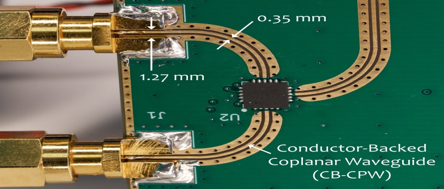
              5. What is a grounded coplanar waveguide (GCPW) and why is it used?

              GCPW is a transmission line structure where the RF trace is flanked by ground on both sides with a ground plane below.

              It is preferred for microwave PCBs because it offers:

              • Excellent isolation
              • Consistent impedance
              • Low radiation loss
              • Compact routing for dense layouts

              This makes it ideal for RF microwave PCB solutions in 5G and radar applications.

              6. Do microwave PCBs require special surface finishes?

              Yes. Surface finishes impact insertion loss and skin effect at GHz frequencies.

              Recommended finishes:

              • Immersion Silver (IAg) → lowest loss
              • ENEPIG → stable & reliable for wire bonding
              • ENIG → commonly used but slightly higher loss

              Avoid heavy plating thicknesses that increase skin resistance.

              7. Does the thickness of a microwave PCB affect performance?

              Absolutely. PCB thickness affects:

              • Impedance
              • Loss tangent
              • Coupling
              • Antenna bandwidth
              • Propagation delay

              Thinner boards generally provide better high-frequency performance and smaller trace widths.

              8. How small can a microwave PCB be?

              Microwave PCBs can be extremely compact (millimeter scale), but size is often dictated by:

              • Antenna requirements
              • Transmission line spacing
              • Ground via placement
              • Heat management

              For mmWave modules (24–80 GHz), PCBs are often less than 20 × 20 mm.

              9. Can microwave PCBs support high power?

              Some can, but it depends on the material.

              Ceramic-filled PTFE laminates like RO3006/3010 support higher power due to:

              • Better thermal stability
              • Lower expansion
              • Higher breakdown voltage

              Always calculate thermal dissipation for PA circuits.

              10. How do you test a microwave PCB?

              Common testing methods include:

              • Time Domain Reflectometry (TDR) – impedance
              • Vector Network Analyzer (VNA) – S-parameters
              • Insertion loss and return loss measurement
              • Phase stability tests
              • Thermal cycling / reliability testing

              Certified manufacturers provide full RF test reports.

              11. What causes failure in a microwave control board?

              Typical failure points include:

              • Overheating of high-power components
              • Delamination of PTFE materials
              • Dielectric breakdown
              • Trace burns or micro-cracking
              • Faulty solder joints
              • Moisture absorption in high-frequency laminates

              Environmental stress factors accelerate failures at GHz speeds.

              12. How long does it take to manufacture a microwave PCB?

              Lead times depend on stackup complexity:

              • Simple 2–4 layer microwave PCB: 7–10 days
              • Hybrid PTFE/FR4 stackups: 10–15 days
              • Advanced mmWave designs (20–80 GHz): 15–25 days

              Prototype + testing may take longer.

              13. Are microwave PCBs expensive?

              Yes, they cost more than standard FR4 because materials like Rogers/PTFE have higher prices and require specialized equipment.

              Cost is influenced by:

              • Material grade
              • Layer count
              • Precision machining
              • Tight impedance tolerance
              • Surface finish

              Large-scale production reduces cost significantly.

              14. How do I source microwave PCBs with UL/CE certification?

              Choose a manufacturer that specializes in RF & microwave PCB solutions and provides:

              • UL-recognized laminates
              • CE-compliant process control
              • Rogers, Taconic, and Arlon material handling
              • Impedance test reports
              • Cleanroom lamination for hybrid constructions

              15. Can microwave PCBs be multilayer?

              Yes. Many microwave designs use 4–12 layer stackups, with PTFE or hydrocarbon layers sandwiched between FR4.

              Common structures include:

              • PTFE outer layers + FR4 inner layers
              • Full PTFE stack for ultra-low-loss radar systems
              • PTFE + ceramic for mmWave phased arrays

              16. What is the maximum frequency a PCB can support?

              It depends on the laminate.

              Typical limits:

              • FR-4: < 6 GHz (with losses)
              • Rogers 4000 series: ~20–40 GHz
              • PTFE-based materials: 40–110 GHz
              • Ceramic-filled materials: up to 110+ GHz and mmWave bands

              For 5G, radar, and satellite systems, PTFE or ceramic laminates are recommended.

              17. Do microwave PCBs require controlled dielectric thickness?

              Yes. Dielectric thickness tolerance is critical because it directly affects:

              • Impedance accuracy
              • Coupling and isolation
              • Phase delay
              • Overall microwave matching performance

              High-frequency PCB fabricators must maintain ±10% or even ±5% dielectric thickness tolerance for mission-critical use.

              18. Why is copper roughness important in microwave PCBs?

              At microwave and mmWave frequencies, skin depth becomes extremely small.
              Rough copper dramatically increases:

              • Conductor loss
              • Insertion loss
              • Heating

              Many designers specify rolled annealed (RA) copper or low-profile copper (VLP/LP) to keep losses under control.

              19. Can microwave PCBs be made flexible (RF flex circuits)?

              Yes—flexible microwave PCBs use materials like:

              • Rogers 3000 series flexible laminates
              • Polyimide-based low-Dk materials

              Applications include antennas, phased arrays, and wearable radar sensors.

              20. What is the expected lifetime of a microwave PCB?

              With proper material selection and thermal design:

              • Consumer microwave PCBs: 5–10 years
              • Automotive radar PCBs: 10–15 years
              • Aerospace/military microwave PCBs: 20+ years

              Failure is usually caused by thermal cycling, moisture absorption, or RF overstress.

              21. How long does it take to manufacture microwave PCBs?

              Typical lead times:

              • Standard microwave PCB: 10–15 days
              • Complex multilayer microwave PCB: 15–25 days
              • Hybrid stack-up with PTFE: 20–30 days

              Fast-turn service (5–7 days) is possible but more expensive.

              22. What Is the Typical Thickness of a Microwave PCB?

              Dielectric layers:

              • 0.127 mm
              • 0.254 mm
              • 0.508 mm
              • 0.8 mm

              Final PCB thickness:

              0.4–1.6 mm depending on application.

              23. What Are the Main Applications of Microwave PCBs?

              Microwave PCBs are used in:

              • 24/60/77 GHz automotive radar
              • 5G mmWave radio units
              • Microwave antennas
              • Satellite transceivers
              • PA/LNA modules
              • RF filters and couplers
              • Medical microwave imaging
              • Wireless base stations
              • Military radar systems

              Above are the common questions that we faced during working, if you have any other questions about microwave PCBs or radio frequency PCBs, just feel free to contact us.

              You may also like

              What is a Microwave PCB? An Ultimate Guide 2026

              December 3rd, 2025

              A microwave PCB handles signals that run at very high frequencies, and these boards support systems that need clean, stable performance. You will find a microwave PCB in equipment such as radar modules, satellite links, high-speed wireless platforms, and precision test devices. As industries push toward higher data rates and smaller RF systems, the need for dependable microwave boards grows quickly.

              Today, many engineers search for rf microwave PCB options that keep loss low and impedance steady. Others look for complete rf & microwave PCB solutions that simplify material choice, stack-up planning, and manufacturing. If you’re evaluating RF microwave PCB materials or sourcing RF & microwave PCB solutions, this article will give you a complete understanding.

              What is a Microwave PCB? An Ultimate Guide 2026

              What Is a Microwave PCB?

              A microwave PCB is a printed circuit board designed to operate at extremely high frequencies, typically:

              • Microwave band: 300 MHz – 30 GHz
              • Millimeter-wave (mmWave): 30 – 100+ GHz

              At these frequencies, PCB traces behave like transmission lines, and even tiny layout variations can impact signal loss, phase accuracy, antenna performance, and overall system reliability.

              Microwave PCBs are commonly used in radar systems, satellite communication, aerospace navigation, and 5G mmWave modules. Compared with standard RF boards, microwave PCBs demand more precise materials, controlled impedance, and stricter fabrication tolerances.

              What Materials Are Used for Microwave PCBs?

              Material choice is one of the most important decisions in microwave design. Standard FR-4 cannot support microwave frequencies due to high loss and unstable dielectric properties. Instead, microwave PCBs use advanced materials engineered for low loss and tight dielectric tolerances.

              Here are the materials most commonly used:

              Material TypeExamplesFeaturesBest Use Case
              PTFE (Teflon)RT/duroid 5880, Taconic TLYExtremely low loss, stable Dk, best for high GHzRadar, mmWave, satellites
              Hydrocarbon CeramicsRogers RO4350B, RO4003CLow loss, easy to manufacture, cost-effective1–20 GHz microwave circuits
              Ceramic-Filled PTFERogers RO3006/3010Ultra-stable Dk, low thermal expansionHigh-power microwave and phased arrays
              Hybrid StackupsFR4 + RogersPerformance + lower costMixed-signal RF/microwave designs

              The best material depends on target frequency, environmental exposure, and mechanical requirements. Each laminate affects loss, phase stability, and long-term reliability.

              Key Design Rules and Layout for Microwave PCB Design

              Designing a microwave PCB is very different from routing a standard digital or low-frequency board. At microwave frequencies, each copper trace behaves like a transmission line. Small changes in width, dielectric height, copper roughness, or via structure can shift impedance and alter the entire RF chain. Because of that, layout and stack-up design must follow strict engineering rules to keep signal quality stable.

              Key Design Rules and Layout for Microwave PCB Design

              Below are the core principles used by RF engineers when building reliable microwave layouts.

              1. Maintain Tight Impedance Control

              Stable impedance is the foundation of microwave design. Even small dimensional changes can introduce reflections or distort the waveform.

              Key requirements:

              • Define target impedance early (commonly 50Ω or 75Ω).
              • Choose the correct structure: microstrip, stripline, or grounded coplanar waveguide (GCPW).
              • Keep trace width consistent along the entire path.
              • Maintain stable dielectric thickness and copper thickness.
              • Use field-solver tools (ADS, HFSS, CST, Polar SI, or Altium impedance calculator).
              • Keep differential pairs phase-matched if used in RF mixers or high-frequency paths.

              GCPW is widely used for microwave PCB design because it offers strong field confinement and supports compact layouts.

              2. Use Smooth Routing Instead of Sharp Corners

              High-frequency energy does not like sudden changes. Sharp corners cause impedance shifts and increase local reflections.

              Preferred routing practices:

              • Avoid 90° turns.
              • Use gradual curves (arc routing) for cleaner field transitions.
              • Use mitered 45° bends if space is limited.
              • Keep sensitive paths straight and short whenever possible.

              Smooth routing helps preserve phase stability and reduces insertion loss.

              3. Keep the Ground Plane Continuous

              A microwave signal needs a clean, uninterrupted return path. Gaps in the ground plane cause radiation, coupling, and impedance drift.

              Ground plane guidelines:

              • Maintain a solid ground layer directly under RF traces.
              • Avoid splits, voids, or cutouts beneath the signal path.
              • Do not place digital return paths through RF areas.
              • Add stitching vias around RF traces to create a “via fence” barrier.

              A well-designed ground structure stabilizes the electromagnetic field and reduces unwanted emissions.

              4. Manage Vias Carefully

              A via is not just a hole at microwave frequencies—it’s a small inductor. Too much via inductance can degrade signal quality.

              Best practices for vias:

              • Avoid unnecessary layer jumps.
              • Use multiple parallel vias to lower effective inductance.
              • Keep via barrels short when possible.
              • Add grounding vias around pads and connectors to improve shielding.
              • Avoid routing RF traces directly over via fields or ground voids.

              Good via strategy can significantly improve stability in PA, LNA, and filter sections.

              5. Select the Right Transmission Line Structure

              Different RF paths require different structures depending on frequency, isolation, and mechanical constraints.

              Common options:

              • Microstrip – simple, ideal for top-layer routing.
              • Stripline – fully shielded, good for noise-sensitive circuits.
              • Grounded coplanar waveguide (GCPW) – excellent isolation, compact layout, and easy impedance tuning.
              • Wide microstrip – lower conductor loss, suitable for power amplifiers.

              GCPW has become the most popular for microwave work due to its predictable behavior and high routing density.

              6. Align Components with the Signal Flow

              Component orientation affects load matching and return loss.

              Component placement guidelines:

              • Place RF blocks (filter, LNA, PA, mixer) in the order of the signal chain.
              • Keep matching networks close to device pins.
              • Avoid unnecessary gaps between RF parts.
              • Place RF connectors, such as SMA or SMP, near the board edge for clean transitions.

              When Should You Choose Microwave PCB vs. RF PCB?

              Many engineers compare microwave PCBs with standard RF boards because both handle high-frequency signals. But the decision depends on frequency, performance targets, and loss tolerance.
              TechnologyFrequency RangeBest For
              RF PCBUp to ~6 GHzBluetooth, Wi-Fi, sub-6 GHz communication
              Microwave PCB6–100+ GHz5G mmWave, radar, satellite, high-precision sensing

              Choose an RF PCB when:

              • Frequencies are below 6 GHz
              • Cost is a major concern
              • FR-4 or mixed-material stackups are acceptable

              Choose a Microwave PCB when:

              • You operate above 6 GHz
              • You require ultra-low loss
              • Your system needs stable phase and predictable impedance
              • Applications involve radar, mmWave, or satellite links

              In short, microwave PCBs suit high-precision projects where even small layout or material changes can affect real performance. They are the preferred choice for radar, satellite links, and advanced communications.
              Microwave PCBs Applications & Industries

              Microwave PCBs appear in many sectors because they support stable, low-loss transmission for sensitive circuits. You’ll often see them in systems that require fast data, long-range signal paths, or precise sensing.

              Common applications include:

              • 5G and 6G wireless infrastructure
              • Satellite communication systems (SATCOM)
              • Automotive radar (24 GHz, 77 GHz)
              • Military and commercial radar platforms
              • Microwave filters, couplers, and antennas
              • High-frequency power amplifiers
              • Navigation and guidance systems
              • Medical imaging devices such as MRI coils
              • Instrumentation and RF test equipment
              • Industrial microwave heating and sensing

              These industries rely on microwave boards because small performance shifts can affect overall system behavior. Stable materials and predictable routing keep these systems accurate and responsive.

              Microwave PCBs Applications & Industries

              Does Size of a Microwave PCB Affect Its Application?

              Yes, board size can influence performance because microwave signals respond to physical dimensions. At these frequencies, even a few millimeters can change how energy travels.

              Board size affects:

              • Impedance stability:Longer traces add more loss and potential phase distortion.
              • Resonance behavior:Larger boards can introduce unwanted resonances.
              • Shielding structure:Compact layouts may need tighter via fences.
              • Thermal changes:Bigger boards may expand more under heat, shifting dielectric spacing.
              • Antenna performance:Antenna length and board shape affect radiation patterns.

              Small boards require sharper tolerance control. Large boards demand stronger handling of expansion and material stability. The ideal size depends on whether the circuit is an antenna, filter, amplifier, or sensor.

              How to Tell If a Microwave Control Board Is Bad?

              Many users ask this because microwave ovens and industrial microwave systems depend on small control boards. Failures are often easy to spot once you know what to check. Common signs of a bad microwave control board include:

              • No power, no response, or blank display
              • Buttons that fail to react
              • Burning smell or visible damage
              • Unusual noises or sparking
              • Microwave stops heating while lights and fan still work
              • Random behavior such as auto-starting or shutting off
              • Relays that click repeatedly without function

              If above signs occur, you can perform below visual checks safely:

              • Scorch marks or dark spots
              • Swollen capacitors
              • Cracked solder joints
              • Damaged connectors
              • Loose ribbon cables

              These symptoms point to circuitry or relay failure. For home microwaves, technicians often replace the entire board rather than repair individual components.

              How Much Does It Cost to Repair a Microwave Circuit Board?

              Repair cost depends on equipment type, part availability, and labor requirements.

              Typical consumer microwave repair ranges:

              • Basic repair: USD 80–120
              • Control board replacement: USD 120–250
              • High-end or built-in models: USD 180–350

              Industrial microwave equipment repair ranges:

              • Board-level component repair: USD 250–600
              • Full board replacement: USD 400–1,200+ depending on complexity

              Factors that influence cost include:

              • Part scarcity
              • Board size and layer count
              • Number of relays, sensors, or high-voltage circuits
              • Whether the board is conformal-coated
              • Testing and calibration requirements

              Consumer microwaves are often cheaper to replace than repair, but industrial microwave systems usually justify board-level repair. EBest Circuit (Best Technology) can repair the microwave circuit board for free if your PCB are ordered from our company.

              Where to Get RF Microwave PCB Boards with UL/CE Certification?

              Many companies need microwave PCBs that meet safety and compliance standards, especially when the final product enters global markets. UL and CE certifications help confirm material reliability and safety. When sourcing certified microwave boards, a good supplier should provide:

              • UL-certified laminates (Rogers, Taconic, Arlon, Panasonic)
              • CE-compliant production and testing
              • Rogers/PTFE/ceramic microwave PCB fabrication
              • Controlled impedance testing reports
              • Hybrid laminations and multi-layer microwave stackups
              • RF & microwave PCB solutions for 1–100 GHz

              EBest Circuit (Best Technology) is a strong option for RF and microwave PCB production because the company offers:

              • UL-approved material systems
              • Stable performance with PTFE, Rogers, and ceramic-filled substrates
              • Tight impedance control for microwave designs
              • Complete CE-related documentation support
              • Strong engineering assistance during stack-up and DFM review
              • Consistent production with IPC standards
              • Fast global delivery for prototypes and batches

              If you are preparing a new microwave PCB or RF hardware program, welcome to contact us at sales@bestpcbs.com, our team is 24/7 hours online for you!

              You may also like

              What is Female N Type to Male SMA Type Adapter?

              December 3rd, 2025

              A Female N Type to Male SMA Type Adapter is a passive radio frequency (RF) component designed to create a seamless and reliable connection between two different types of coaxial connectors: a female N-type port and a male SMA-type. This article will demystify this essential adapter, exploring its function, common types, key applications, and how to select the right one for your project, ultimately linking its performance to the critical role of high-quality PCB and PCBA manufacturing.

              Sourcing the correct interconnect components can be frustrating and costly, leading to project delays and performance issues. What are the most common pain points when dealing with RF adapters like the N female to SMA male?

              • Signal Loss and Mismatch:​ Using adapters with poor impedance control (deviating from 50Ω) causes signal reflections, increased VSWR, and degraded system performance.
              • Incompatibility Confusion:​ Difficulty distinguishing between SMA, RP-SMA, and N-type interfaces leads to ordering mistakes, wasted resources, and rework.
              • Mechanical Failure:​ Low-quality adapters with poor plating or weak structural integrity can break, loosen, or wear out quickly, especially in field-testing environments.
              • Frequency Limitations:​ Selecting an adapter not rated for the required frequency band (e.g., using a low-frequency adapter for a high-frequency application) results in unexpected signal attenuation.
              • Supply Chain Inconsistency:​ Difficulty finding a reliable manufacturer capable of delivering high-performance, consistent-quality adapters PCB circuit in both prototype and production volumes.

              These challenges highlight the need for a supplier that understands both the component and the underlying RF principles. The solution lies in partnering with a manufacturer with expertise that extends from the connector itself to the printed circuit boards it interfaces with.

              • Precision Impedance Matching:​ Ensuring strict impedance control (e.g., ±5%) through expert PCB design and manufacturing to minimize signal loss and reflection.
              • Interface Standardization Guidance:​ Providing clear specifications and diagrams to help customers navigate the complex landscape of RF connector types and avoid compatibility errors.
              • Robust Mechanical Construction:​ Utilizing high-quality materials (e.g., gold plating over nickel) and precision machining to ensure durable, reliable connections that withstand mating cycles and harsh environments.
              • Broad Frequency Optimization:​ Designing and testing adapters to perform optimally across their specified frequency range, up to 18 GHz for SMA and higher for N-type.
              • Reliable, Scalable Production:​ Offering end-to-end PCB and PCBA support from PCB prototype to volume production with consistent quality, backed by certifications like ISO 13485, IATF 16949 and AS9100D.

              At BEST Technology, we are not just a PCB manufacturer; we are a specialized provider of high-frequency PCBs and assemblies. Our deep expertise in RF materials like Rogers and our certified, multi-location PCBA facilities ensure that the components you depend on, from adapters to the boards they connect, are built to the highest standards of performance and reliability. Pls feel free to contact us at sales@bestpcbs.com to discuss your project requirements.

              Female N Type to Male SMA Type Adapter

              What Does a Female N Type to Male SMA Type Adapter Do in RF Links?

              PCB → SMA Female → SMA Male (Adapter) → N-Type Female(Adapter)
              In a typical RF board, an SMA female connector is mounted at the board edge as the RF I/O point. The adapter’s SMA male end simply screws onto this PCB-mounted SMA female, turning the board’s SMA interface into an N-type female interface on the spot. In other words, the adapter acts as a mechanical and electrical “front end change,” converting the PCB’s small SMA port into a larger, rugged N-type interface without altering the PCB design.

              In essence, this adapter acts as a bridge. Its primary function is to enable a connection between equipment or cables that would otherwise be incompatible due to their different connector genders and types. This is crucial in RF systems where maintaining a continuous, controlled impedance path is paramount to signal integrity.

              • Interface Conversion:
                It physically mates a device with a female N-type (typically a larger, more robust connector used for base stations or outdoor equipment) to a cable with a male SMA (common on smaller devices like GPS modules, Wi-Fi cards, or test equipment).
              • Impedance Continuity:
                A high-quality adapter is engineered to maintain a constant characteristic impedance (almost always 50 Ohms for these connectors) through the transition.
                This prevents impedance discontinuities that cause signal reflections, leading to loss and measurement inaccuracies.
              • Signal Pathway Extension:
                It allows for the flexible configuration of test benches and operational systems without requiring custom-made cables, saving time and cost during system integration or troubleshooting.

              In summary, the female N type to male SMA type adapter​ is a fundamental tool for ensuring connectivity and signal fidelity across diverse RF components.

              What Are the Common RF Adapter Types Used Between N-Type, SMA, and RP-SMA Interfaces?

              Understanding the “family” of adapters helps prevent costly mistakes. The main categories are defined by the connector interfaces they bridge.

              The threads define whether a connector is male or female:
              If the connector has inner threads, it is male.
              If it has outer threads, it is female.
              This rule is the same for both SMA and RP-SMA connectors.

              The center contact defines the polarity:
              “Reverse polarity” in RP-SMA only refers to the gender of the center contact, not the threads.

              In a standard SMA connector:
              • a male connector has an inner threads + center pin,
              • a female connector has a outer threads + center socket.

              In an RP-SMA connector, this is reversed:
              • an RP-SMA male has an inner threads + center socket,
              • an RP-SMA female has a outer threads + center pin.

              Center pinCenter receptacle
              Internal threadSMA male/plugRP-SMA male/plug
              External threadRP-SMA female/jackSMA female/jack
              Female N Type to Male SMA Type Adapter

              N-Type ↔ SMA Series

              This is the standard series. Both N and SMA connectors have a sexed interface: male connectors have an inner threads + center pin, and female connectors have a outer threads + center socket.

              • N Female to SMA Male:​ Connects a device with an N-type female to a cable with an SMA male.
              • N Male to SMA Female:​ Connects a device with an SMA female to a cable with an N-type male.

              N-Type ↔ RP-SMA Series

              The “Reverse Polarity” (RP-SMA) interface was created as a proprietary measure to prevent connection with standard consumer equipment. The gender of the center conductor is reversed.

              • RP-SMA Male to N Type Female:​ The RP-SMA male has a center socket (instead of a pin), and it mates with an N-type female.
              • N-Type Male to RP-SMA Female:​ The RP-SMA female has a center pin, and it mates with an N-type male.

              Adapter Interface Specifications

              Adapter TypeEnd 1End 1 ThreadEnd 1 Center ContactEnd 2End 2 ThreadEnd 2 Center Contact
              RP-SMA Male to N Type FemaleRP-SMA MaleInner ThreadCenter Socket
              (RP Style)
              N-Type FemaleOuter ThreadCenter Socket
              N Type Male to RP-SMA FemaleN-Type MaleInner ThreadCenter PinRP-SMA FemaleOuter ThreadCenter Pin (RP Style)

              This classification clarifies the relationships, ensuring you select the correct N type female to SMA male adapter​ or its RP-SMA counterpart for your specific need.

              When Should Engineers Use an N Type Female to SMA Male Adapter?

              This specific adapter is frequently deployed in specific scenarios where equipment interoperability is key.

              • Connecting Test Equipment to Antennas:​ When a vector network analyzer (VNA) with an N-type output port needs to test a device or antenna with an SMA connector, this adapter provides the necessary link.
              • Base Station Integration:​ To interface a macro-cell base station (often using robust N-type connections) with a smaller, SMA-based repeater or a femtocell unit.
              • Lab and Development Environments:​ During R&D, when prototyping with SMA-ended evaluation boards but needing to connect to larger, N-type-based infrastructure cables for range or durability.

              The decision to use an N type female to SMA male adapter​ is driven by the need for a reliable, low-loss transition between equipment tiers of different physical scales and connector standards.

              How Does an N Type Male to SMA Female Adapter Support Stable Signal Conversion?

              The stability of the signal conversion hinges on the precision manufacturing of the adapter itself, a process deeply connected to high-quality PCB and assembly principles.

              • Precision Center Conductor Alignment:
                The internal center pin and socket must be perfectly aligned to ensure a smooth, low-resistance electrical path.
                Any misalignment creates an impedance bump, disrupting the signal.
              • Dielectric Material Quality:
                The insulator (often Teflon) must have stable electrical properties and low loss to prevent signal attenuation, especially at higher frequencies.
              • Robust Outer Connector Body:
                A sturdy, well-plated outer shell provides consistent grounding and shielding against electromagnetic interference (EMI), which is critical for signal integrity.

              Therefore, an N type male to SMA female adapter​ from a quality supplier functions as a seamless extension of the transmission line, not a compromise.

              Why Do Wireless Devices Often Need an RP SMA Male to N Type Female Adapter Cable?

              Many consumer wireless devices, such as Wi-Fi routers and drones, use RP-SMA connectors on their external antenna ports to comply with regulatory standards. However, professional-grade external antennas or test equipment often use standard N-type connectors.

              • An RP SMA male to N type female adapter cable​ is essential to connect these consumer devices to a more robust or specialized antenna system.
              • This is common in applications like enhancing cellular reception with an external antenna or connecting a Wi-Fi device to a spectrum analyzer for testing.

              How to Pick the Right RP SMA Male to N Type Female Adapter for Field Testing?

              Field testing demands durability and reliability. When selecting an adapter, consider:

              • Frequency Range:
                Ensure the adapter’s specified frequency range covers your application (e.g., 2.4 GHz/5 GHz for Wi-Fi, higher for 5G).
              • Construction Quality:
                Look for features like a hex crimp nut for easy hand-tightening, a stainless steel body, and gold-plated contacts for corrosion resistance.
              • VSWR Specification:
                VSWR is read as a ratio, and lower values are always better. A value near 1:1 means very little signal is reflected.
                For an RP SMA Male to N Type Female Adapter, a VSWR of around 1.20:1 is considered good.
                Values near 1.10:1 indicate excellent quality, while anything above 1.50:1 shows noticeable mismatch.
                If the VSWR approaches 2.0:1, the adapter is poor quality and will degrade RF performance.
              VSWR RangePerformance MeaningQuality Level
              1.10:1 – 1.20:1Very low reflection, excellent matchingHigh quality
              ≤ 1.25:1Good for most RF field testsGood quality
              1.30:1 – 1.50:1Noticeable mismatch beginsAverage
              ≥ 2.00:1Strong reflection, unstable performancePoor quality

              Choosing the right RP SMA male to N type female adapter​ ensures accurate measurements and prevents failures in demanding outdoor environments.
              Why Choose an SMA Female to N Type Male Adapter for Compact RF Modules?

              Compact RF modules (e.g., Bluetooth or Zigbee modules) often have SMA female connectors due to their small size.

              To connect these modules to a larger system using N-type cables, an SMA female to N type male adapter​ is the ideal solution.

              It provides a secure, impedance-matched interface without putting mechanical stress on the module’s small PCB-mounted connector.

              How to Select the Best Female N Type to Male SMA Type Adapter for Your Project?

              Selecting the right RF adapter is critical for system performance. The best choice is not always the most expensive one, but the one that optimally balances key specifications with your project’s requirements and budget.

              1. Electrical Specifications

              These parameters determine if the adapter will work in your application at all.

              • Frequency Range:​ The adapter must support your system’s highest frequency.
                • Standard Grade (up to 6-8 GHz):​ Suitable for Wi-Fi, 4G-LTE, and general applications.
                • Precision Grade (up to 12-12.5 GHz):​ Ideal for test and measurement, point-to-point radio.
                • High-Performance (up to 18+ GHz):​ Necessary for R&D and high-frequency instrumentation.
                • Guidance:​ Always select an adapter with a frequency rating exceeding your system’s maximum operating frequency.
              • Voltage Standing Wave Ratio (VSWR):​ Measures impedance matching; a value closer to 1.00 is ideal. A high VSWR causes signal reflection and power loss.
                • Guidance:​ Review the supplier’s VSWR-vs-Frequency chart to ensure it meets your requirements (e.g., <1.25:1) across your operating band.
              • Impedance:​ The standard for most RF applications is 50 Ohms; simply confirm this value.
              • Insertion Loss:​ Represents the signal power lost through the adapter. While lower is better, it requires careful consideration.
                • Key Trade-off:​ Ultra-low loss demands superior materials and precision manufacturing, which increases cost.
                • Low-Frequency/Short-Range:​ Loss differences are minimal; a cost-effective adapter is often sufficient.
                • High-Frequency/Critical Applications:​ Investing in a low-loss model is necessary for signal integrity.

              2. Mechanical Specifications:

              These factors impact physical robustness, mating cycle life, and ease of use.

              • Connector Gender/Type:​ You have specified a Female N-Type​ (outer thread) to Male SMA​ (inner thread) adapter.
              • Mating Torque:​ High-quality adapters specify a recommended tightening torque (e.g., 8 in-lbs for SMA). Over-tightening can damage the connector.
              • Plating:​ The finish determines corrosion resistance, durability, and electrical conductivity.
                • Internal Contacts:​ Typically gold-plated for excellent conductivity and oxidation resistance. Thicker gold plating enhances longevity.
                • External Shell:​ Often nickel-plated for corrosion resistance, with a final finish of gold, silver, or passivation.
              • Cable Interface (if applicable):​ For cable assemblies, also consider the cable’s specifications (e.g., diameter, flexibility) and the quality of the connector attachment.

              3. Environmental Needs:

              The adapter must survive and perform reliably in your project’s environment.

              • Operating Temperature Range:
                • Commercial:​ -10°C to +70°C
                • Industrial:​ -40°C to +85°C
                • Military:​ -55°C to +125°C
              • Moisture & Corrosion Resistance:​ For harsh environments (marine, industrial), look for stainless steel construction and robust plating. An IP rating for dust/water ingress protection may be necessary.
              • IP Rating:​ For outdoor or wash-down environments, specify a sealed adapter with an appropriate IP rating (e.g., IP67).

              4. Supplier Reliability:

              The supplier’s reputation is your guarantee of performance and a stable supply chain.

              • Proven Track Record:​ Prioritize established RF component manufacturers and distributors (e.g., Huber+Suhner, Pasternack, Amphenol, Rosenberger) known for quality and consistency.
              • Comprehensive Documentation:​ Reliable suppliers provide detailed datasheets with full electrical specifications and S-parameter plots.
              • Quality Certifications:​ Look for ISO 9001 quality management system certification, especially for production volume purchases.

              Ultimate Balance: Performance, Robustness, and Cost

              The “best” adapter is defined by your project’s specific priorities. Use the following table as a guide:

              Project TypeRecommended Adapter GradePriorityExample Suppliers
              Consumer Electronics / Basic IoTStandard Grade (up to 6 GHz)Cost-EffectivenessValue-line brands on major distributor websites (e.g., Digi-Key, Mouser)
              Communications Equipment / Test SystemsPrecision Grade (up to 12.5 GHz)Performance & Reliability BalancePasternack, Amphenol RF
              R&D / High-End InstrumentationHigh-Performance (up to 18+ GHz)Performance Above AllHuber+Suhner, Rosenberger
              Military / Aerospace / Harsh EnvironmentsMilitary-Grade, Stainless SteelDurability & Environmental ResilienceSpecialist military-grade manufacturers

              In summary, the selection process involves clearly defining your electrical, mechanical, and environmental needs, and then choosing a high-quality adapter from a reputable supplier that meets those requirements without exceeding your necessary performance threshold and budget.

              Why Does Adapter Performance Depend on High-Quality PCB and PCBA Production?

              While an adapter may seem like a simple mechanical part, its core performance is an extension of precision RF engineering, which is rooted in PCB and PCBA expertise.

              High-Frequency PCB Precision That Supports Stable Adapter Performance

              • An RF adapter can only perform as well as the PCB it connects to.
              • High-frequency launches, trace geometry, and impedance transitions must be fabricated with tight tolerances to avoid added loss or reflections.
              • EBest Circuit (Best Technology) specializes in RF PCB fabrication with precise impedance control and consistent stackup accuracy, ensuring that SMA or N-type adapters mounted on the board operate with predictable, low-loss performance.

              RF Material Expertise Ensuring Low-Loss Transitions

              • Many adapters connect directly to traces routed on Rogers, PTFE, hydrocarbon laminates, or hybrid RF stackups.
              • Our team has extensive experience processing these materials, enabling cleaner transitions, lower dielectric loss, and stable RF behavior across multi-GHz bands.
              • The result is an adapter-to-PCB interface that preserves signal integrity rather than degrading it.

              Reliable PCBA Assembly for Robust Connector Mounting

              • The mechanical reliability of an RF adapter depends on how well it is soldered and supported on the PCB. Poor solder joints or insufficient anchoring can cause intermittent behavior, impedance jumps, or connector damage.
              • With SMT factories in China and Vietnam, EBest Circuit (Best Technology) delivers high-precision assembly for SMA, N-type, MMCX, U.FL, and other RF connectors, ensuring dependable long-term stability.

              Surface Finishes Optimized for Long-Term RF Contact Integrity

              • The performance of an RF adapter ultimately relies on the pad finish it mates with.
              • EBest Circuit (Best Technology) provides specialized surface treatments—ENIG, ENEPIG, immersion silver, hard gold—chosen according to frequency requirements, durability, and corrosion resistance.
              • A stable, low-resistance contact surface ensures the adapter maintains consistent RF performance over thousands of mating cycles.

              Certified Manufacturing That Supports Consistent RF PCB Quality

              • RF systems demand predictable, repeatable quality.
              • EBest Circuit (Best Technology) operates under AS9100D, IATF16949, ISO13485, and ISO9001, ensuring strict process control from PCB prototypes, fabrication to final assembly.
              • This allows engineers to trust that each PCB and PCBA batch will interact with their N-type or SMA adapters exactly as intended, from prototype builds through full-scale production.

              Therefore, partnering with a manufacturer like BEST Technology, which holds certifications like AS9100D and IATF 16949 and has over 19 years of experience with high-frequency materials, guarantees that the components integral to your RF system. Our integrated approach from PCB fabrication to PCBA assembly ensures consistency and quality from the ground up.

              Female N Type to Male SMA Type Adapter

              To conclude, a Female N Type to Male SMA Type Adapter​ is a critical interconnect component that ensures signal integrity and compatibility between different RF interfaces. This article has detailed its functions, varieties, and selection criteria, emphasizing that optimal performance is achieved only through precision manufacturing. The reliability of such RF components is inextricably linked to the quality of the underlying manufacturing processes, particularly in PCB and PCBA. BEST Technology leverages its expertise in high-frequency PCB materials, stringent impedance control, and certified, scalable production capabilities to support the creation of reliable RF systems. For your next radio frequency adapter PCB or PCBA project requiring robust interconnect solutions, pls feel free to contact our experts at sales@bestpcbs.com.

              You may also like

              What is Radio Frequency PCB? RF PCB Design Guidelines

              December 2nd, 2025

              When it comes to wireless systems—WiFi, Bluetooth, cellular IoT, radar, GPS, or any RF module—the performance of the radio frequency PCB (RF PCB) directly determines signal integrity, radiation efficiency, and product stability. A radio frequency PCB operates in high-frequency environments where small layout changes may shift impedance, weaken gain, or create unwanted noise. Because of this, a radio frequency PCB requires strict engineering rules, carefully selected materials, and a routing method that protects signal quality.

              This article explains what an RF PCB is, the characteristics you must consider, the right FR PCB materials, the correct RF PCB routing rules, and a complete RF PCB design guideline you can follow for your next high-frequency design. Hope this guide is helpful and give you a best solution to design your RF PCB.

              What is Radio Frequency PCB? RF PCB Design Guidelines

              What Is a Radio Frequency PCB?

              A radio frequency PCB, or RF PCB, refers to a board used to transmit and receive signals at high frequencies—from hundreds of megahertz to multiple gigahertz. These boards are widely used in wireless modules, IoT devices, GPS systems, consumer electronics, radar sensors, and communication infrastructure.

              Unlike standard FR4 boards, RF PCBs involve dedicated dielectric materials, controlled impedance structures, and strict layout rules to keep signal integrity stable. The entire PCB—from stack-up to routing—must support predictable propagation velocity, stable loss characteristics, and smooth energy flow.

              RF PCBs are used in:

              • Wireless modules
              • GPS receivers
              • Sub-GHz transmitters
              • 5G communication units
              • Radar sensors
              • IoT devices
              • RF amplifiers and mixers
              • Antenna feed circuits

              Their performance depends on trace geometry, ground stability, and how cleanly the RF path is designed.

              What Is a Radio Frequency PCB?

              What Is a Radio Frequency PCB?

              Characteristics of an RF PCB

              RF PCBs typically have the following characteristics:

              • Controlled impedance routing for RF signal paths
              • Low-loss PCB materials to minimize attenuation
              • Stable dielectric constant (Dk) over temperature and frequency
              • Strict EMI/EMC requirements
              • Short, direct RF trace routing
              • Careful grounding strategy (dedicated ground plane, stitching vias)
              • Special treatment around matching networks and antenna feeds

              Because RF energy behaves like waves rather than simple electrical current, the PCB becomes part of the RF system itself—meaning the layout, stack-up, and materials must be engineered for high-frequency behavior.

              What Is the Frequency Range of RF PCB?

              RF PCBs typically operate in the following ranges:

              Frequency BandRangeTypical Applications
              Low RF300 MHz – 1 GHzISM band, sub-GHz transmitters
              Mid RF1 GHz – 6 GHzWi-Fi, Bluetooth, GPS
              High RF6 GHz – 30 GHz5G, radar
              Millimeter Wave30 GHz – 80 GHzAutomotive radar, high-speed links

              Most IoT devices today (BLE, WiFi, Zigbee, Sub-GHz RF) fall between 433 MHz – 6 GHz.

              What Is the Best PCB Material for RF?

              Choosing the right laminate affects signal quality, trace accuracy, and overall loss.

              • FR4 PCB Material

              FR PCB material, typically FR4, works for low-frequency RF designs below 2.4 GHz. It offers low cost and good mechanical strength. However, its dielectric properties vary with temperature and frequency. Loss tangent is higher than PTFE, so it works best for short RF paths or low-power consumer wireless modules.

              • Rogers RF Materials

              Rogers laminates such as RO4350B, RO4003C, and RO5880 are widely used for RF designs due to:

              • Low loss tangent
              • Very stable dielectric constant
              • Smooth copper surface
              • High processing consistency

              These materials are ideal for GPS, radar, Wi-Fi 6, UWB, sub-6G, and millimeter-wave applications.

              • PTFE / Teflon Laminates

              PTFE offers excellent RF performance, especially for microwave and radar. It has very low loss and highly stable characteristics. Fabrication needs tight process control due to soft substrate behavior.

              • Ceramic Substrates

              Ceramics substrate provide strong thermal stability and high dielectric precision. They work well in high-power RF amplifiers, satellite communication modules, and advanced radar systems.

              Here is a common radio frequency PCB material table:

              SubstrateTg (°C)Td (°C)DkLoss TangentBand
              FR4~135~295< 4.4~0.022 (parasitic ignored)X–K
              Isola MT402003603.38–3.750.0028–0.0035W
              IS680 AG-3482003603.480.0029W
              IS680 AG2003603.00–3.480.0020–0.0029W
              IS6802003602.80–3.450.0025–0.0035W
              Isola MT772003603.000.0017W
              Rogers 3003NR5003.000.0013W
              Rogers 3006NR5006.150.0022X–Ka
              Rogers 4360>2804076.150.0038X–Ka
              RT Duroid 6010.2LMNR50010.700.0023X–Ka
              RT Duroid 6202NR5002.900.0015X–Ka
              RT Duroid 6006NR5006.450.0027X–Ka
              RT Duroid 6035NRNR3.500.0013X–Ka

              (Note: NR means Not Reported)

              PCB Design Guide for Radio Frequency RF Boards

              Designing RF PCBs involves stack-up planning, controlled impedance, grounding, spacing, matching networks, and EMI reduction. Below are the recommended RF PCB guidelines and routing rules you can apply to achieve stable wireless performance.

              1. Start With Complete RF Design Information

              Successful RF PCB design begins long before the first trace is drawn. Engineers must collect all essential RF parameters to avoid redesigns later. This includes:

              • Functional description and operating frequency band
              • Current and voltage requirements of each RF stage
              • RF component list and package dimensions
              • PA gain, receiver sensitivity, and system isolation targets
              • Planned PCB stack-up structure
              • Controlled impedance values
              • Mechanical constraints and enclosure limits
              • Shielding frame or metal-can dimensions
              • Matching network reference designs
              • Simulation results for power amplifiers and LNAs

              Gathering this information early ensures that layout decisions align with system-level RF performance.

              PCB Design Guide for Radio Frequency RF Boards

              PCB Design Guide for Radio Frequency RF Boards

              2. Physical Zoning of the RF PCB

              Physical zoning organizes the board according to how RF signals flow.

              • RF Signal Flow Placement

              Place RF components in the exact order of the signal chain. A short, direct, and linear path minimizes insertion loss, improves impedance stability, and preserves gain.

              • RF Component Orientation

              Rotate filters, PAs, LNAs, couplers, and mixers so their input/output pins align with the straightest possible RF path. Avoid unnecessary detours or bends.

              • Isolation Through Ground Structures

              To prevent RF coupling and cross-interference, isolate RF sections using:

              • Ground shielding walls
              • Via-fence structures
              • Shield cans over sensitive circuits
              • Copper barriers or partitions

              These structures keep RF and digital noise apart, improving overall stability.

              PCB Design Guide for Radio Frequency RF Boards

              3. Electrical Zoning

              Electrical zoning separates different circuit domains so they cannot interfere with each other.

              • Power section: Power management ICs, regulators
              • Digital control section: MCUs, logic circuits, clocks
              • Analog RF section: LNAs, PAs, filters, mixers, antennas

              These zones should not overlap in routing. Digital switching noise or PLL jitter can easily couple into RF paths if the layout is not properly divided.

              4. RF Transmission Line Structures

              RF PCBs commonly use one of three controlled-impedance transmission line types:

              Microstrip Line

              • RF trace on the top layer
              • Continuous ground plane directly beneath (Layer 2)
              • Impedance determined by trace width and dielectric height
              • Ideal for simple and low-to-mid–frequency RF designs.
              Microstrip Line

              Stripline

              • RF trace routed on an inner layer
              • Sandwiched between two solid ground planes
              • Provides superior isolation and uniform impedance
              • Useful in compact or high-frequency designs where shielding is critical.
              Stripline

              Grounded Coplanar Waveguide (GCPW)

              • Top-layer trace with ground on both sides
              • Ground plane below the trace
              • Excellent isolation and impedance control
              • Often preferred when space is tight or when multiple RF lines run in parallel.
              Grounded Coplanar Waveguide (GCPW)

              5. Impedance Selection and Calculation

              Achieving the correct characteristic impedance (typically 50Ω) requires considering:

              • Trace width
              • Copper thickness
              • Dielectric constant (Dk)
              • Dielectric height between layers

              Use tools such as Polar SI9000 or your PCB manufacturer’s impedance calculator.

              Impedance Selection and Calculation

              6. RF Trace Bending Rules

              Straight RF traces are ideal, but bends are sometimes unavoidable.

              Follow these rules:

              • Minimum bend radius ≥ 3× trace width
              • Avoid 90° bends (cause impedance discontinuity)
              • Use 45° bends or smooth arc/bowed shapes
              • Apply mitering to compensate for impedance changes

              For critical RF links, simulate bends in an EM solver to validate performance.

              7. Layer Transitions for RF Traces

              RF traces should stay on one layer. If a layer change is unavoidable:

              • Use two vias at minimum
              • Via diameter should match the RF trace width
              • When space is tight, use three smaller vias in parallel

              Multiple vias reduce via inductance and minimize impedance mismatch.

              8. Signal Isolation Rules

              Isolation is as important as impedance control in RF design.

              a) RF Lines

              • Keep RF traces well separated
              • Avoid long parallel runs
              • Use GCPW for noisy or densely packed areas
              • Keep sensitive microwave lines away from high-power circuits

              b) High-Speed Digital Signals

              • Route digital clocks on different layers
              • Avoid crossing beneath RF paths
              • Switching noise can modulate RF signals if not isolated

              c) Power Lines

              • Use a dedicated power layer for stable distribution
              • Place bypass capacitors close to RF IC power pins
              • Keep power traces away from RF transmission lines

              9. Ground Area Design

              Ground integrity determines the quality of RF performance.

              • Use solid, continuous ground planes
              • Avoid slots, gaps, and return-path interruptions
              • Do not route signals across RF ground regions
              • Add abundant ground stitching vias
              • Reduce inductance in ground loops

              In RF PCB design, a 4-layer RF PCB design is widely considered the most balanced structure for modern wireless modules because it provides stable impedance, strong isolation, and efficient routing without dramatically increasing manufacturing cost. While 2-layer boards are cheaper and 6-layer boards offer more routing space, the 4-layer stack-up delivers the best performance-to-cost ratio for most RF applications under 6 GHz.

              Below is the recommended stack up:

              • Layer 1 (Top Layer): RF traces + components
              • Layer 2 (Ground Plane): Continuous ground reference
              • Layer 3 (Power Plane): Power routing + local shielding below RF areas
              • Layer 4 (Bottom Layer): Non-critical routing or power distribution

              RF PCB Routing Rules You Must Follow

              1. The length of the RF traces should be kept as short as possible, and ensure that the surrounding densely arranged holes are shielded. The intervals should be approximately 50 mils.

              2. RF traces must not have vias, meaning they cannot cross layers. It is preferable to use 135° angle traces or circular traces.

              3. Near the RF traces, there should be no high-frequency signal lines. Pay attention to the UART signal line being shielded by a ground layer, and add ground holes around it for protection.

              4. The RF traces should be as close as possible to the size of the pads.

              5. For the RF traces, matching networks and the area around the antenna socket > 0.8mm, copper cannot be laid; they need to be hollowed out.

              6. The RF traces should be kept as far away from the battery holder as possible, with a distance of at least 5mm or more.

              7. A π-type matching circuit needs to be reserved on the RF path, and this π-type matching circuit should be placed close to the chip end like below diagram show:

              RF PCB Routing Rules You Must Follow

              IPC Standards for Radio Frequency PCB

              The following IPC standards are typically referenced for RF PCB and high-frequency designs:

              • IPC-6018 – Qualification and Performance Specification for High Frequency (Microwave) PCBs
              • IPC-2221/2222 – General & rigid PCB design rules
              • IPC-2141 – Controlled impedance design
              • IPC-TM-650 – Test methods for dielectric materials
              • IPC-4103 – High-frequency base materials

              These standards help ensure reliability, board performance, and manufacturability for RF and microwave applications.

              Your Reliable RF PCB Manufacturer – EBest Circuit (Best Technology)

              Best technology is an experienced RF PCB manufacturer in China, we offer stack-up consultation, material selection, transmission line simulation, and impedance guidance for complex RF modules. Our production lines use SI9000 modeling, fine etching control, and well-controlled lamination parameters. Our radio frequency PCB manufacture capability including:

              • Rogers, SY, Isola, PTFE, and hybrid RF PCB materials
              • Tight-tolerance controlled impedance
              • 4–10 layer high-frequency stack-ups
              • Laser drilling, buried/blind vias
              • Ceramic-filled dielectric PCB options
              • Full DFM & design support for RF modules and antennas

              In addition to this, we offer one-stop PCB & PCBA service covers RF tuning, antenna matching, shielding assembly, coaxial connector installation and final functional RF tests.

              Whether you’re building Bluetooth modules, RF front ends, radar circuitry, or custom antennas, our engineering team ensures high yield and reliable RF performance—helping you bring your wireless product to market faster.

              FAQs about RF PCBs

              1. What materials are recommended for radio frequency PCB?

              Rogers RO4350B, RO4003C, RO5880, PTFE, and high-stability ceramics work best for RF or microwave applications.

              2. Can I use FR4 for RF PCB?

              Yes, if the operating frequency is low and the RF path is short. Many 433 MHz and 2.4 GHz consumer modules still use FR4.

              3. Why should RF traces avoid vias?

              A via adds inductance and disrupts impedance. RF energy prefers a continuous layer.

              4. What routing structure is most common?

              Microstrip and grounded coplanar waveguide are widely used due to predictable impedance.

              5. Does EBest Circuit (Best Technology) support RF PCBA assembly?

              Yes, including antenna tuning, shielding, coaxial connector mounting, and final RF testing.

              You may also like

              Reliable BNC PCB Solutions for Precision RF Connectivity

              December 2nd, 2025

              BNC PCB refers to the integration of BNC (Bayonet Neill–Concelman) connectors directly onto printed circuit boards, providing a robust interface for RF (radio frequency) signals in applications ranging from test equipment to communication devices. This article explores the types, selection criteria, layout practices, and performance considerations for implementing BNC connectors on PCBs, with a focus on achieving reliable high-frequency connectivity.

              Are you struggling with signal loss, impedance mismatches, or mechanical instability in your RF designs? Many engineers face recurring challenges when integrating coaxial interfaces like BNC connectors onto PCBs. Common frustrations include:

              • Poor impedance continuity leading to signal reflections and degraded performance.
              • Mechanical strain causing connector loosening or PCB pad damage.
              • Inadequate grounding strategies that increase electromagnetic interference (EMI).
              • Difficulty selecting the right connector type (vertical, right-angle, or edge-mount) for spatial and electrical needs.
              • Time-consuming prototyping cycles due to footprint or layout errors.

              These issues can be systematically addressed with thoughtful design and manufacturing support. Here’s how a specialized PCB provider can help:

              • Impedance-controlled routing ensures minimal signal distortion from connector to trace.
              • Robust anchoring features (like through-hole pins or metal brackets) enhance mechanical stability.
              • Optimized ground plane design and via fencing reduce EMI and crosstalk.
              • Expert guidance on connector selection based on frequency, space, and mounting orientation.
              • Rapid prototyping services with validated footprints to accelerate development.

              At BEST Technology, we specialize in high-frequency PCB solutions, including precision-engineered BNC interconnects. Our team supports your design with impedance-matching expertise, durable board materials, and fast turnaround for prototypes and production. A warm welcome to contact us at sales@bestpcbs.com to discuss your project requirements.

              BNC PCB

              What is a BNC PCB?

              A BNC PCB incorporates a BNC connector—typically a BNC PCB connector—directly mounted to the board, serving as a coaxial interface for RF signals. These connectors use a bayonet coupling mechanism for quick, secure connections and are designed to maintain a 50-ohm or 75-ohm characteristic impedance.

              • Signal Support:
                The BNC PCB connector preserves signal integrity by providing a shielded path from the cable to the PCB traces.
                Its coaxial structure minimizes EMI, while the board layout ensures impedance continuity between the connector’s center conductor and the microstrip or stripline transmission line.
              • Applications:
                Commonly used in video equipment, RF test instruments, and data communication systems where frequent connection cycles and RF performance are critical.
                In summary, a BNC PCB enables efficient RF signal transition between external cables and internal circuitry, with careful attention to impedance matching and shielding.
              BNC PCB

              ​What Types of BNC Connector PCB Mount Options Are Most Common in RF Boards?

              Engineers can choose from several mounting styles, each suited to different mechanical and spatial constraints.

              • Vertical Mount (BNC PCB mount):
                The connector stands perpendicular to the board, ideal for applications where space is limited in the horizontal plane.
              • Right-Angle Mount (BNC connector PCB mount right angle):
                The connector body parallels the board, saving vertical height—useful for compact modules or stacked assemblies.
              • Edge Mount (BNC edge mount PCB):
                Installed on the board’s edge, often used when the connector must align with an enclosure panel.
              • Surface-Mount or Through-Hole:
                Through-hole versions offer stronger mechanical retention, while surface-mount types suit automated assembly.
                The BNC connector PCB mount style is selected based on layout density, cable orientation, and shielding requirements.

              How Do You Choose the Right BNC Female PCB Mount Connector for Your Design?​

              Selecting the appropriate BNC female PCB mount connector involves evaluating electrical, mechanical, and environmental factors.

              • Impedance: Ensure the connector matches the system impedance (e.g., 50 ohms for most RF applications).
              • Frequency Range: Standard BNC connectors perform up to 4 GHz; verify the model’s rated frequency.
              • Mounting Style: Choose vertical, right-angle (BNC female right angle solder PCB mount connector), or edge-mount based on space and cable routing.
              • Termination Type: Soldering (through-hole or surface-mount) vs. crimping; through-hole provides better strain relief.
              • Material and Plating: Brass with gold or nickel plating ensures corrosion resistance and stable conductivity. A well-chosen BNC female PCB connector minimizes VSWR (voltage standing wave ratio) and withstands mating cycles.

              What Layout Rules Matter Most When Creating a Reliable BNC Connector PCB Footprint?​

              The BNC connector PCB footprint must maintain impedance integrity and mechanical stability. Key rules include:

              • Impedance Matching: Design the pad pattern and adjacent ground structures to match the connector’s characteristic impedance (e.g., 50 ohms).
              • Grounding: Place grounding vias near the connector’s shield pins to create a low-inductance path to the ground plane.
              • Pad Size and Shape: Follow the manufacturer’s datasheet to avoid tombstoning or solder voids.
              • Keep-Out Zones: Avoid placing components or traces under the connector body to prevent short circuits.
              • Strain Relief: Include metal anchors or epoxy trenches for high-vibration environments. A precise BNC PCB footprint is critical for signal fidelity and long-term reliability.

              When Should Engineers Use a BNC Right Angle PCB Mount Instead of a Vertical One?​

              A BNC right angle PCB mount is preferred when:

              • Vertical Space is Limited:
                Such as in slimline instruments or stacked PCBs.
              • Cable Routing Constraints:
                The cable must exit parallel to the board to avoid sharp bends.
              • Panel-Mount Alignment:
                The connector interfaces with a side-panel port. In contrast, a vertical BNC PCB mount is better when cables connect from above, as in rack-mounted equipment.
                The right-angle version (90 degree BNC PCB mount) reduces mechanical leverage on the PCB, lowering the risk of pad lifting.

              How Does an Ultra-Tiny BNC Jack PCB Help in Compact RF Modules?​

              An ultra-tiny bnc jack pcb(e.g., sub-miniature versions) saves space without sacrificing performance. Benefits include:

              • High Density: Enables more connectors per board area in portable devices.
              • Lightweight Design: Critical for aerospace or handheld instruments.
              • Preserved Performance: Maintains impedance control and shielding despite smaller dimensions. These jacks are ideal for high-density RF systems like multi-channel data acquisition boards.

              What Routing Practices Improve Performance When Working With a 90 Degree BNC PCB Mount?​

              For a 90 degree BNC PCB mount, follow these routing guidelines:

              • Impedance Continuity: Use controlled-impedance traces from the connector pin to the IC, avoiding abrupt width changes.
              • Minimal Stub Length: Keep the transition from the connector pad to the main trace as short as possible.
              • Ground Plane Integrity: Ensure an unbroken ground plane beneath the trace; add grounding vias near the connector.
              • Avoid Sharp Bends: Use curved or 45-degree trace bends to reduce reflections. Proper routing ensures that the BNC right angle PCB maintains low VSWR and insertion loss.
              BNC PCB

              Why Do RF Teams Rely on EBest Circuit (Best Technology) for BNC Prototype PCB Production?​

              RF teams choose EBest Circuit (Best Technology) for BNC prototype PCB manufacturing due to:

              • Impedance Expertise: We control dielectric thickness and trace geometry to achieve precise impedance matching.
              • High-Frequency Materials: Expertise with Rogers, Taconic, or FR-4 hybrids for optimal RF performance.
              • Rapid Prototyping: Quick-turn services with validated designs to accelerate testing.
              • Quality Assurance: Rigorous testing for VSWR, insertion loss, and mechanical stability. Our capability to produce reliable BNC prototype PCB assemblies reduces iteration cycles and ensures performance compliance.

              In a nutshell, BNC PCB solutions enable precise RF connectivity by integrating robust coaxial interfaces directly onto circuit boards. This guide has detailed connector selection, layout techniques, and routing practices to ensure signal integrity in high-frequency designs. At BEST Technology, we combine engineering support with advanced manufacturing to deliver reliable BNC PCBs for prototyping and production. Pls feel free to reach out to us at sales@bestpcbs.com for your next RF PCB project.

              FAQs about BNC PCB

              Is BNC better than SMA?

              • BNC offers quick bayonet coupling for frequent connections but is typically rated to 4 GHz. SMA uses a threaded interface for higher frequencies (up to 18 GHz) and better EMI shielding. Choose BNC for ease of use in lower-frequency applications.

              Is BNC better than Ethernet?

              • BNC is designed for RF signals (e.g., video, radio), while Ethernet (RJ45) carries digital data. They serve different purposes; BNC provides superior impedance control for analog RF.

              Is BNC the same as RF?

              • BNC is a type of RF connector. “RF” is a broad term for radio frequency signals, while BNC refers to a specific connector family commonly used for RF interconnects.

              How to crimp a BNC?

              • Strip the coaxial cable to expose the center conductor and shield. Insert the center conductor into the connector pin and crimp. Slide the shield braid over the body, and crimp the outer sleeve. Use a BNC crimping tool for consistent results.

              You may also like

              Custom MMCX PCB Design for Mini RF Modules

              December 2nd, 2025

              MMCX PCB is the backbone of modern miniaturized radio frequency (RF) modules, providing the critical interface for high-frequency signal transmission in extremely limited spaces. This comprehensive guide explores everything from connector selection and design best practices to manufacturing advantages, equipping you to master custom MMCX PCB design for your compact wireless devices.

              Do you struggle to balance performance, size, and reliability in your mini RF modules? You’re not alone. Designing with MMCX PCB connectors presents unique challenges:

              • Signal degradation from impedance mismatches.
              • Mechanical failure due to poor connector choice or board mounting.
              • Complex layout constraints in high-density designs.
              • Difficulty sourcing reliable, high-quality MMCX PCB.
              • Managing costs while meeting stringent RF performance specs.

              The good news is that these challenges have proven solutions. By focusing on a few key areas, you can achieve robust and high-performing designs.

              • Precise impedance control calculations and simulation prevent signal issues.
              • Selecting the correct MMCX PCB mount connector type ensures mechanical stability.
              • Adhering to RF-optimized layout rules overcomes space constraints.
              • Partnering with an experienced RF MMCX PCB manufacturer​ guarantees component quality.
              • Optimizing the design for manufacturability from the start controls costs.

              At BEST Technology, we specialize in best possible high-frequency PCB solutions. Our great technical expertise ensures your custom MMCX PCB design​ is built with rigorous quality control, superior materials, and rapid turnaround. Pls feel free to contact us at sales@bestpcbs.com to bring your mini RF module to the real life.

              MMCX PCB

              What Is an MMCX PCB?

              An MMCX PCB integrates Micro-Miniature Coaxial (MMCX) connectors directly onto a printed circuit board, creating essential RF interfaces for compact wireless devices. This configuration is particularly valuable for space-constrained applications where reliable high-frequency connections are critical.

              Key Characteristics:

              • Miniaturization:​ MMCX connectors are significantly smaller than traditional RF connectors like SMA, making them ideal for modern compact electronics.
              • Board-Level Integration:​ These connectors are designed specifically for PCB mounting, providing a permanent and robust RF interface solution.
              • High-Frequency Capability:​ Properly designed MMCX PCBs maintain signal integrity at frequencies up to 6 GHz, suitable for most wireless applications.

              The effectiveness of an MMCX PCB design hinges on maintaining precise impedance control and ensuring a seamless transition from the connector to the PCB’s transmission lines.

              MMCX PCB

              Types of MMCX PCB Connectors Used Today

              Selecting the appropriate MMCX connector type is fundamental to achieving both optimal electrical performance and mechanical stability in your design.

              Primary Connector Variants:

              1. By Orientation:
                • Vertical Mount:​ Standard orientation for straightforward vertical cable connection
                • Right-Angle Mount (MMCX R PCB):​ Ideal when cable routing parallel to the board surface is preferred
              2. By Gender Configuration:
                • Standard Gender:​ Conventional male/female pairing
                • Reverse Polarity (MMCX LR PCB):​ Gender-reversed versions used for specific compatibility requirements
              3. By Mounting Style:
                • Surface Mount (SMD):​ Preferred for automated assembly and space-constrained designs
                • Through-Hole:​ Offers enhanced mechanical strength for high-vibration environments

              Understanding these options enables designers to select the most suitable MMCX PCB connector​ for their specific application requirements.

              How to Choose the Right MMCX PCB Mount Connector?

              Selecting the optimal connector requires careful consideration of multiple technical and practical factors.

              Selection Criteria:

              1. Performance Requirements:
                • Frequency range and insertion loss specifications
                • Impedance matching (typically 50Ω) and VSWR requirements
              2. Mechanical Considerations:
                • Expected mating cycles and durability needs
                • Board space constraints and height restrictions
                • Cable exit direction and strain relief requirements
              3. Manufacturing Factors:
                • Compatibility with automated assembly processes
                • Soldering temperature tolerance and thermal mass

              A systematic evaluation against these criteria ensures the selected MMCX PCB mount connector​ will meet both performance and reliability targets.

              MMCX Male PCB vs MMCX Female PCB Differences

              Selecting the correct connector gender for PCB mounting is critical for both mechanical integrity and electrical performance in RF designs. The primary differences lie in their physical structure, typical applications, and design implications.

              1. Physical Structure and Interface

              • MMCX Female PCB Connector (Jack):
                This component features an internal receptacle with a slotted, spring-loaded center contact.
                It is the standard interface soldered onto the board.
                The MMCX female PCB connector​ is designed to accept and grip the male pin, providing a secure and reliable connection.
              • MMCX Male PCB Connector (Plug):
                This type has a central pin that extends from the connector body.
                The MMCX male PCB​ is inserted into the female jack, and the connection is maintained by the jack’s internal spring mechanism.
              MMCX PCB

              2. Typical Applications and Usage

              • Standard Board-Level Interface (Female Jack):
                The MMCX female connector PCB mount​ is the predominant choice for the fixed connection point on a circuit board.
                It is used for connecting to antenna cables, external modules, or test equipment.
                Its design protects the central mating interface from physical damage.
              • Specialized Applications (Male Plug):
                The MMCX male PCB​ connector is less common. Its typical uses include:
                • Board-to-Board Interconnects:​ Directly connecting two PCBs in a stacked or coplanar configuration.
                • Adapter Boards:​ Functioning as an MMCX PCB adapter​ on a small circuit board to convert interfaces.
                • Specific Cable Exit Requirements:​ Used when a particular mechanical layout demands a male connector on the board itself.

              3. Design and Sourcing Considerations

              • Mechanical Reliability:
                The female jack, once soldered to the PCB, generally offers better resistance to mechanical stress because its sensitive internal parts are housed and protected.
                The protruding pin of a male connector is more susceptible to bending or damage.
              • Polarity and System Planning:
                Using a standard MMCX female PCB jack​ simplifies system design, as most cables are terminated with male plugs.
                Employing a male connector on the board requires careful planning to ensure cable and interoperability.
              • Supply Chain Simplification:
                The MMCX female PCB connector​ is a standard, widely available component.
                Opting for this standard streamlines sourcing and reduces compatibility risks compared to the less common male-board-mount variant.

              In summary, for most designs where the PCB serves as the fixed base for a removable cable, the MMCX female PCB connector​ is the recommended and conventional choice. The MMCX male PCB​ connector is reserved for specific, specialized interconnect scenarios.

              MMCX PCB Jack Design Points for RF Stability

              Achieving RF stability requires meticulous attention to both component selection and layout implementation.

              Critical Design Considerations:

              1. Footprint Accuracy:
                • Strict adherence to manufacturer-recommended land patterns
                • Proper pad dimensions and spacing for reliable soldering
              2. Impedance Continuity:
                • Smooth transition from connector pin to transmission line
                • Controlled trace width matching the system impedance (50Ω)
              3. Grounding Implementation:
                • Continuous ground plane beneath the connector
                • Strategic via placement for effective RF return paths

              Proper implementation of these design principles ensures the MMCX PCB jack​ maintains signal integrity across the required frequency spectrum.

              How MMCX PCB Adapter and MMCX Pigtail Improve Routing?

              MMCX PCB adapters and pigtails offer distinct and complementary solutions for overcoming spatial and mechanical challenges in compact RF module design. They enhance flexibility, reliability, and performance by redefining the connection point between the PCB and the external RF world.

              1. MMCX PCB Adapter:

              An MMCX PCB adapter is a board-mounted component that provides a permanent interface conversion.

              • Function:​ It acts as a standardized port on your PCB, typically converting the MMCX interface larger, more common type like SMA.
              • Routing & Design Improvement:
                • Saves Space:​ Allows the use of a tiny MMCX footprint on the PCB while enabling connection to standard test equipment cables without a dedicated, space-consuming SMA connector.
                • Facilitates Testing:​ Provides a robust, dedicated point for connecting test equipment (e.g., vector network analyzers) during development and debugging, preventing damage to fragile direct solder points.
                • Design Reusability:​ A single PCB design can be adapted for different external connectivity needs simply by changing the onboard adapter.

              2. MMCX Pigtail:

              An MMCX pigtail is a short, flexible cable with a pre-attached connector.

              • Function:​ It creates a short, shielded RF bridge between the PCB and a component like an antenna.
              • Routing & Design Improvement:
                • Decouples Component Placement:​ It physically separates the antenna or sensor from the main PCB, allowing it to be positioned optimally for performance (e.g., away from interference, near a housing window) without being constrained by the PCB’s location.
                • Absorbs Stress:​ The flexible cable absorbs strain, vibration, and torsion that would otherwise transfer directly to the solder joints of a board-mounted connector, significantly improving mechanical reliability and long-term durability.
                • Simplifies Assembly:​ Enables modular assembly, where the PCB and antenna can be installed separately and connected last, streamlining the manufacturing process.

              Summary:

              ComponentSolves This ProblemPrimary Benefit
              MMCX PCB Adapter​Interface incompatibility and need for test pointsProtocol Conversion​ on the board itself.
              MMCX Pigtail​Physical layout constraints and mechanical stressSpatial Flexibility​ and Strain Relief.

              In practice, these components are often used together. For example, a PCB might feature an MMCX PCB adapter​ for external connectivity, while an internal MMCX pigtail​ connects to an antenna mounted elsewhere inside the device. This combination delivers maximum routing flexibility and reliability for custom MMCX PCB designs in mini RF modules.

              China RF MMCX PCB Manufacturing Advantages

              Partnering with specialized manufacturers offers distinct benefits for producing high-quality RF circuits.

              Key Advantages:

              1. Technical Expertise:
                • Extensive experience with high-frequency materials (Rogers, Taconic)
                • Sophisticated impedance control capabilities (±5% or better)
              2. Economic Benefits:
                • Competitive pricing without compromising quality
                • Efficient supply chain management reducing lead times
              3. Comprehensive Support:
                • Design for manufacturability (DFM) feedback
                • Rapid prototyping and volume production flexibility

              These advantages make partnering with a specialized RF MMCX PCB manufacturer​ a strategic choice for developing high-performance wireless modules.

              How to Request RF MMCX PCB Quotes from a Factory?

              Obtaining accurate quotations requires providing comprehensive project information.

              Essential Documentation:

              1. Technical Specifications:
                • Complete Gerber files with all layer stack-up details
                • Detailed bill of materials (BOM) with component specifications
              2. Requirements Definition:
                • Quantities needed (prototype vs. production volumes)
                • Impedance control requirements and testing criteria
                • Required delivery timeline and quality expectations

              Providing clear, complete information enables manufacturers to generate accurate RF MMCX PCB quotes​ and identify potential production issues early in the process.

              MMCX PCB is well-suited for compact medical electronics, delivering stable RF performance in space-limited designs. They are frequently integrated into devices such as portable patient monitors and pulse oximeters due to their reliable signal transmission. With ISO 13485 certification, EBest Circuit (Best Technology) supports full-process MMCX PCB manufacturing and SMT MMCX PCB assembly services. If you have a project to discuss, feel free to submit your requirements through the contact form on our Contact Us page.

              MMCX PCB

              Ultimately, an MMCX PCB is a precision component that forms the reliable RF link in today’s miniaturized wireless electronics. Mastering its design, from connector selection to layout and manufacturing partnership, is key to module success. BEST Technology combines engineering expertise with stringent quality control to deliver high-performance custom MMCX PCB solutions​ that meet your specifications and timeline. For your next mini RF module project, pls feel free to contact our team at sales@bestpcbs.com for a consultation and quote.

              You may also like

              Stable Quality RF Connector PCB with Fast Delivery

              December 2nd, 2025

              An RF connector PCB is a specialized printed circuit board designed to interface with radio frequency connectors, ensuring stable signal transmission in high-frequency applications. This article provides a comprehensive guide to RF connector PCBs, covering types, materials, layout considerations, and how to select the right components for your needs.

              Are you struggling with signal loss, unreliable connections, or delays in sourcing radio frequency boards? Many engineers encounter challenges when integrating RF components into their designs. Common pain points include:

              • Impedance mismatch leading to poor signal integrity.
              • Difficulty selecting the right PCB material for specific frequency ranges.
              • Complexities in RF connector PCB layout causing performance issues.
              • Challenges in sourcing mini RF PCB connectors for compact designs.
              • Long lead times and unstable quality from suppliers.

              Fortunately, these challenges can be overcome with expert manufacturing support. As a specialized RF PCB producer, we address these issues by:

              • Implementing precise impedance control techniques.
              • Offering a range of high-frequency materials like Rogers and Taconic.
              • Providing DFM support for optimal RF connector PCB layout.
              • Supplying various mini RF PCB connectors for space-constrained applications.
              • Ensuring stable quality and fast delivery through advanced manufacturing processes.

              As a reliable RF PCB manufacturer in China, BEST Technology specializes in high-frequency PCB solutions, combining rigorous quality control with rapid turnaround times to meet your project requirements. Whether you require a simple SMA connector PCB prototype or a complex multilayer RF PCB design with stringent impedance control, BEST Technology has the specialized engineering expertise to deliver reliable solutions. Pls feel free to contact us at sales@bestpcbs.com for reliable RF connector PCB solutions.

              RF Connector PCB

              What is RF Connector PCB?

              An RF connector PCB is a PCB engineered to host RF coaxial connectors and provide a controlled-impedance signal transition from the connector to the PCB’s RF traces, ensuring stable high-frequency performance. These boards are engineered to maintain characteristic impedance (typically 50Ω or 75Ω) and minimize signal loss across high-frequency ranges.

              1. Core Function: The primary role is to provide a stable transition from the PCB’s transmission lines to various PCB mount RF connectors, such as SMA female angle PCB mount RF connector​ or vertical mount PCB RF connector​ types.
              2. Key Characteristics: They feature precise dielectric materials and controlled geometries to preserve signal integrity up to GHz ranges.
              3. Applications: Commonly used in telecommunications, radar systems, and high-speed data applications.

              In summary, the RF connector PCB is a fundamental component in any high-frequency electronic system, ensuring reliable signal transmission between the board and external RF components.

              What is the Best PCB Material for RF?

              In practical RF PCB applications, designers commonly work within the 500 MHz to 3 GHz range, which covers most wireless communication and IoT systems. Frequencies above 3 GHz generally fall into the microwave domain. Selecting the proper PCB material is crucial for optimal RF performance. The “best” material depends on your specific frequency, loss, and cost requirements.

              1. FR-4 for Entry-Level RF Designs (Below ~2.5–3 GHz)

              FR-4 can still be used in many low-to-mid RF applications when cost is the priority.

              When FR-4 Works Well

              • Operating frequency below 2.5–3 GHz
              • Short RF trace lengths
              • Moderate insertion-loss tolerance
              • Consumer-grade wireless products (BLE, WiFi 2.4 GHz, NB-IoT, RFID)

              Limitations

              • Dielectric constant varies with frequency and temperature
              • Higher loss tangent causes signal attenuation in long RF traces
              • Not suited for multi-GHz precision RF connectors (e.g., 2.92 mm)

              Usage Strategy

              Many engineers use hybrid stackups:
              FR-4 for non-RF layers + a high-frequency laminate for the RF layer.

              2. Rogers Laminates for Stable, Low-Loss RF Structures

              Rogers materials are widely considered the industry standard for RF PCBs.

              Advantages

              • Very stable dielectric constant (Dk):≈ 2.9–3.7
              • Very low loss tangent (Df):≈ 0.001–0.003
              • Excellent impedance consistency
              • Ideal for SMA connectors, IPEX interfaces, micro RF connectors, and other high-frequency transitions.
              • Strong performance up to 10–15 GHz, providing significantly more bandwidth capability than typical RF PCB applications require.

              Common Grades for RF Connector PCBs

              RO4003C → best cost/performance balance
              RO4350B → higher thermal stability
              RO4835 → oxidation-resistant for higher reliability

              Application Scenarios

              • LTE, WiFi, GNSS front-ends
              • RF connector transition zones(SMA, SMB, 2.92 mm edge-mount)

              Rogers is often the first choice for stable-quality RF connector PCBs.

              3. Taconic Laminates for Higher-Frequency or Stricter Loss Requirements

              Taconic materials perform exceptionally well in microwave and low-mmWave ranges but are also suitable for high-end RF PCBs.

              Advantages

              • Ultra-low loss tangent
              • Strong dimensional stability
              • PTFE-based options suitable for precision launch structures

              Best Use Cases

              • Suitable for microwave applications in the 3 GHz to 10 GHz range.
              • Radar, satellite, phased-array antennas
              • RF connector regions requiring extremely low VSWR

              For regular RF PCB (500 MHz–3 GHz), Taconic is a premium option when you want lower loss than Rogers but can accept higher cost.

              4. Isola High-Speed Materials for Mixed RF + Digital PCB Designs

              Isola laminated materials are ideal for boards combining RF and high-speed digital.

              Advantages

              • Good electrical stability up to 6–20 GHz
              • Lower cost compared with top-end RF laminates
              • More compatible with multi-layer constructions and HDI

              Usage Scenarios

              • Multi-layer RF/digital mixed systems
              • WiFi routers, gateways, small base stations
              • Designs requiring balanced performance/cost

              5. How to Choose the Best Material for Your RF Connector PCB

              The choice depends on your engineering priorities:

              Performance Priority

              → Rogers RO4003C / RO4350B

              Ultra-Low Loss or Microwave Range

              → Taconic TLX / RF Series

              Cost-Sensitive RF Products

              → FR-4 or Hybrid Stackup

              Mixed RF + Digital

              → Isola High-Speed Laminates

              To sum up, for most RF connector PCB applications within the 500 MHz–3 GHz range, Rogers RO4003C provides the most consistent balance of low loss, stable dielectric behavior, manufacturability, and cost. FR-4 hybrid structures also work well for budget-sensitive designs. Taconic and Isola materials offer elevated performance for more demanding or mixed-signal applications.

              What are the Common RF Connector PCB Types?

              Various PCB RF connector types​ are available to meet different mechanical and electrical requirements. Understanding these options helps in selecting the right component for your design.

              • SMA Connectors PCB: The most common type, including SMA female angle PCB mount RF connector​ and RP-SMA female adapter PCB edge-mount solder RF connector. Excellent for frequencies up to 18 GHz.
              RF Connector PCB
              • SMB Connectors PCB: Smaller snap-on alternatives, like the PCB type SMB RF connector, suitable for applications up to 4 GHz where space is limited.
              RF Connector PCB
              • Miniature Connectors PCB: This category includes mini RF PCB connector​ and micro RF PCB connectors​ such as IPEX PCB RF connector, designed for compact devices like smartphones and IoT modules.
              RF Connector PCB
              • Edge-Mount Connectors PCB: Such as 2.92 mm edge-mount RF connectors, which require careful attention to PCB thickness​ for proper mounting and performance.
              RF Connector PCB
              • Stacked and Vertical Options: PCB mount stacked RF connector​ and vertical mount PCB RF connector​ save horizontal space on the board.
              RF Connector PCB

              Selecting the correct RF connector PCB type ensures reliable performance and simplifies assembly, contributing to a stable quality RF circuit board. For more information or if you would like to send us any inquiry, please send us an email through the contact form at the bottom of our Contact US Page.

              How is the RF Connector PCB Size?

              The size of an RF connector PCB is determined by the connector’s footprint, the controlled-impedance transmission line requirements, and the mechanical space needed for reliable assembly. Even a small connector can require a broader PCB area once RF constraints are considered.

              1. Connector Footprint and Keep-Out Requirements

              Every RF connector—whether a mini RF PCB connector, IPEX, MMCX/MCX, or SMA female angle PCB mount RF connector—comes with a manufacturer-specified footprint.
              This footprint defines:

              • pad dimensions for the signal and ground pins
              • mounting holes (for flange-type connectors)
              • mechanical keep-out zones under the connector
              • required distance to the PCB edge for edge-mount types

              These constraints establish the minimum PCB area around the connector.

              2. RF Transmission Line Geometry

              The center pin of the connector must transition into a 50-ohm microstrip or stripline.
              The trace width depends on:

              • PCB material (FR-4, Rogers, Taconic)
              • dielectric constant (Dk)
              • core thickness above the ground plane

              For example, a 1.6 mm FR-4 board may require a 2.5–3.0 mm microstrip width.
              This transition also needs space for:

              • a tapered pad-to-trace region
              • anti-pad clearance
              • ground-via fencing along both sides

              These RF structures often increase the required PCB width.

              3. Mechanical Clearance and Grounding Needs

              Additional area is required for:
              • connector installation and solder access
              • avoiding tall components near the mating area
              • dense ground-via rows that provide a low-inductance return path
              • optional reinforcement for high-torque connectors like SMA

              These mechanical factors further influence the PCB outline.

              4. Example: Edge-Mount SMA Connector

              Edge-mount SMA connectors illustrate how size is defined by multiple constraints:

              • PCB thickness must match the connector specification
              • board-edge notches may be required
              • wide RF trace transitions need space
              • ground-via fences must be placed around the landing area

              Thus, even a compact SMA connector results in a relatively wide layout region.

              In summary, RF connector PCB size is not fixed—it emerges from a combination of:
              • connector footprint
              • impedance-controlled RF trace geometry
              • mechanical clearance
              • grounding and via-fence patterns

              The correct approach is always:
              Choose the connector → follow its datasheet → calculate RF geometry → build the PCB layout around these constraints.

              How to Do RF Connector PCB Layout?

              A proper RF connector PCB layout​ is paramount for minimizing losses and reflections. Here are the key considerations.

              • Impedance Matching:
                Use controlled impedance routing (typically 50Ω) from the connector pad to the IC.
                This requires precise calculation of trace width based on the dielectric constant and thickness of the PCB material.
              • Grounding:
                Provide an uninterrupted ground plane adjacent to the RF trace.
                Use numerous grounding vias around the RF coaxial connector PCB​ pad to create a low-inductance return path.
              • Via Placement:
                Minimize the use of vias in the RF path.
                When necessary, use via fencing to suppress unwanted mode propagation.
              • Component Placement:
                Place matching components (like capacitors and inductors) as close as possible to the connector to reduce stray inductance and capacitance.

              A disciplined layout approach, often supported by EM simulation tools, is essential for a successful stable quality RF connector PCB.

              How to Select Mini RF PCB Connector for Compact RF Modules?

              Choosing a mini RF PCB connector​ for compact modules involves balancing size, frequency, and reliability.

              • Frequency Range: Ensure the connector (e.g., IPEX PCB RF connector​ or micro RF PCB connectors) supports your operating frequency without excessive insertion loss.
              • Mating Cycles: Consider the durability required; some miniature connectors have lower mating cycle ratings than full-sized ones.
              • Board Real Estate: Evaluate the footprint and height to ensure it fits within the mechanical constraints of your module.
              • Assembly Process: Check if the connector is suitable for reflow soldering and compatible with your assembly capabilities.

              Selecting the right miniature connector is key to achieving both miniaturization and reliable performance in compact RF designs.

              Design Considerations for SMA Female Angle PCB Mount RF Connector in High-Frequency Boards

              Integrating an SMA female angle PCB mount RF connector​ into a high-frequency board requires specific attention to mechanical and electrical details.

              • Grounding Connection: Ensure the connector’s outer shell has a robust, low-impedance connection to the board ground plane using multiple vias.
              • Board Edge Clearance: For edge-mounted types, maintain the recommended clearance from the board edge to ensure mechanical stability.
              • Impedance Continuity: The transition from the connector’s center pin to the PCB microstrip line must be smooth to avoid impedance discontinuities.
              • Polarization: Utilize the connector’s polarization key (if available) to prevent incorrect mating during field installation.

              Proper design ensures that the SMA female angle PCB mount RF connector​ performs reliably over its intended lifespan.

              Why Choose EBest Circuit (Best Technology) as Your RF Coaxial Connector PCB Supplier?

              BEST Technology​ stands out as your ideal partner for RF coaxial connector PCB​ manufacturing. Selecting the right partner for RF connector PCB manufacturing is critical for achieving stable high-frequency performance. We deliver a combination of engineering depth, manufacturing capability, and quality assurance that RF projects depend on.

              • One-Stop PCB & PCBA Capability:
              We provide complete manufacturing services from RF substrate PCB prototyping, fabrication to full PCBA assembly. So your RF connector PCB, matching networks, shielding blocks, and coaxial interfaces are built under one unified process with consistent quality control.

              • Specialization in High-Frequency PCB Fabrication:
              Our production lines are optimized for RF materials such as Rogers, Taconic, and high-speed Isola, allowing us to meet demanding requirements for dielectric stability, low loss, and controlled impedance across 500 MHz to 3 GHz RF systems.

              • Proven Expertise with Multiple RF Connector Types:
              We support SMA, SMB, MCX, MMCX, IPEX, mini RF PCB connectors, and precision 2.92 mm edge-mount connectors, ensuring that your design receives the correct footprint, mechanical alignment, and RF launch transition.

              • Engineering-Driven RF Layout Support:
              Our technical team understands RF connector PCB layout principles—proper pad geometry, via fencing, return-path control, microstrip/stripline transitions—and provides DFM guidance to help customers avoid common RF pitfalls.

              • Strict Impedance & Signal Integrity Control:
              By using calibrated stackups, impedance modeling, and controlled-etch processes, we maintain consistent 50-ohm transitions from connector pad to RF trace, reducing reflection, insertion loss, and EMI issues.

              • Advanced Quality Assurance Built for RF Boards:
              AOI, impedance testing, X-ray inspection, and microsection analysis are integrated into our process, ensuring that every RF coaxial connector PCB meets its electrical and mechanical specifications before shipment.

              • Fast Turnaround with Stable, Repeatable Quality:
              With streamlined RF manufacturing workflows and in-house process monitoring, we deliver stable quality and reliable lead times, enabling customers to accelerate prototype validation and shorten product launch cycles.

              • Global Customers Trust Our RF Work:
              From wireless communication modules to GNSS front-end boards, radar subsystems, and IoT RF platforms, our RF connector PCBs are used in real-world applications where performance and reliability cannot be compromised.

              In a nutshell, an RF connector PCB is the foundation for reliable high-frequency signal interconnection. This guide has explored the key aspects of designing and sourcing these critical components. For your next RF coaxial connector PCB project, partner with BEST Technology for Stable Quality RF Connector PCBs with Fast Delivery. Our expertise ensures your designs perform as intended. A warm welcome to contact us at sales@bestpcbs.com to discuss your requirements.

              You may also like

              How to Choose the Right RF Circuit Board?

              November 27th, 2025

              An RF circuit board is a specialized printed circuit board designed to operate at radio frequencies, typically from around 100 MHz up to about 2 GHz, where signal integrity and controlled impedance are paramount. Above this range, designs are usually classified as microwave PCBs, which follow similar principles but face even tighter constraints on materials, layout, and loss control. This guide will walk you through the critical considerations—from materials and design to supplier selection—for choosing the right RF PCB for your application.

              Selecting the right RF circuit board is a complex challenge that can make or break the performance of wireless modules, communication systems, and radar equipment. Common frustrations include:

              • Unexpected Signal Degradation:High-frequency signals are susceptible to loss and interference, leading to poor performance.
              • Impedance Control Challenges:​ Achieving and maintaining a consistent characteristic impedance (e.g., 50Ω) is difficult but critical for signal integrity.
              • Material Selection Confusion:​ Choosing the wrong RF PCB material can result in inefficient thermal management and unacceptable dielectric losses.
              • Complex Design and Layout:​ RF PCB design requires specialized knowledge; a small routing error can severely impact functionality.
              • Finding a Reliable Manufacturing Partner:​ Many standard PCB manufacturers lack the expertise and equipment to reliably produce high-quality microwave PCBs.

              Overcoming these challenges is possible with a clear understanding of RF fundamentals and a partnership with an experienced RF printed circuit boards supplier. The solutions directly address these pain points:

              • Superior Materials:​ Utilizing low-loss laminate materials with stable dielectric constants to minimize signal degradation.
              • Precision Engineering:​ Employing advanced design and fabrication techniques to ensure tight impedance control and consistent performance.
              • Expert Material Guidance:​ Providing recommendations on specialized materials like PTFE or ceramic-filled laminates for optimal thermal and electrical properties.
              • Adherence to Strict Design Rules:​ Following established RF PCB design guidelines to avoid common layout pitfalls.
              • Partnering with a Specialized Supplier:​ Choosing a manufacturer like EBest Circuit (Best Technology), which specializes in RF and microwave printed circuit boards, ensures access to the necessary expertise and quality controls.

              At EBest Circuit (Best Technology), we are a specialized manufacturer of high-frequency circuit boards. With 19 years of extensive experience in advanced materials and precise fabrication processes, we are committed to delivering RF circuit boards that meet the most demanding electrical specifications. Pls feel free to contact us at sales@bestpcbs.com to discuss your RF circuit boards project requirements.

              RF Circuit Board

              What Is an RF Circuit Board?

              An RF (Radio Frequency) circuit board is engineered to transmit, receive, and process high-frequency signals typically ranging from hundreds of megahertz (around 100 MHz) up to approximately 2 GHz. Unlike standard PCBs used for low-frequency electronics, the performance of an RF circuit board is highly sensitive to its physical properties—including dielectric constant, layer stack-up, trace geometry, and impedance control—which must be precisely managed to ensure stable, low-loss signal propagation.

              • Core Function:
                The primary role of an RF PCB is to guide RF signals with minimal loss, distortion, or radiation.
                This is crucial in applications like smartphones, GPS units, and wireless networking equipment.
              • Key Characteristics:
                These boards are defined by controlled impedance traces, specific material selection, and specialized structures like ground planes and shielding to contain electromagnetic fields.
                Proper RF circuit board design​ is fundamental to their operation.

              In summary, an RF circuit board is a high-performance platform where the board itself is an integral component of the circuit’s functionality.

              RF Circuit Board

              What Is the RF Circuit Board Material?

              The choice of material is arguably the most critical decision in RF PCB design. Standard FR-4 is often insufficient for high frequencies due to its high loss tangent and unstable dielectric constant.

              • Low Loss Tangent (Df):​ Materials with a low dissipation factor (Df) are essential to minimize energy loss converted into heat. Common options include PTFE (Teflon), ceramic-filled PTFE composites (e.g., Rogers RO4000® series), and hydrocarbon ceramics.
              • Stable Dielectric Constant (Dk):​ A stable dielectric constant (Dk) across frequency and temperature is vital for predictable impedance and phase response.
              • Thermal Management:​ High-frequency circuits can generate heat, so materials with good thermal conductivity (e.g., ceramic-filled laminates) are often preferred.
              • Common Materials:​ Popular RF PCB material​ choices are Rogers RO4350B (a balance of performance and cost), PTFE-based materials for extreme high-frequency applications, and specialized China PTFE laminate circuit boards for RF and microwave industries.

              Selecting the right RF circuit board material​ ensures signal integrity, thermal stability, and overall reliability, forming the foundation of a successful RF PCB project.

              What Are the Differences Between RF and Microwave Printed Circuit Board?

              The terms “RF” and “microwave” are often used interchangeably, but there is a technical distinction that influences design and material choices.

              • Frequency Range:
                While the broader radio frequency spectrum spans from kilohertz up to hundreds of gigahertz, in PCB engineering practice RF PCBs usually refer to boards operating in the ~100 MHz to 2 GHz range, and microwave PCBs to those above 2 GHz.
                As frequency increases, wavelengths shorten, and the circuit board’s physical dimensions become a more critical part of the circuit.
              • Design Complexity:
                Microwave PCB​ design often deals with transmission line effects, wave propagation, and parasitic effects that are less pronounced at lower RF frequencies.
                This requires more sophisticated modeling and simulation.
              • Material Requirements:
                While both require low-loss materials, microwave PCBs​ demand materials with exceptionally stable Dk and ultra-low loss tangents, such as pure PTFE, to function effectively at these higher frequencies.

              In practice, the design principles for RF and microwave printed circuit board​ are similar, but microwave applications push the requirements for precision and material performance to a greater extreme.

              What Parts of a Circuit Board Confine RF Transmission Signals?

              Containing RF energy within designated pathways is essential to prevent interference and signal loss. Key structures achieve this confinement.

              • Controlled Impedance Transmission Lines:​ Microstrips and striplines are the primary conduits. A consistent cross-section and proximity to a ground plane create a controlled electromagnetic field around the trace.
              • Ground Planes:​ A solid, unbroken ground plane beneath signal layers is critical. It provides a return path for the signal and helps contain the electromagnetic field.
              • Shielding:Circuit board RF shielding, often in the form of metal cans or fences soldered to the board, physically isolates sensitive RF sections like amplifiers or oscillators from radiating or receiving interference.
              • Vias:​ A “via fence” or a row of grounding vias around a microstrip line can act as a barrier, further confining the signal and reducing coupling to adjacent circuits.

              Proper RF PCB routing​ and the use of these structures are fundamental to ensuring signals travel only where intended.

              What Is a Radio RF Pass-Through Circuit Board?

              An RF pass-through, or feedthrough, is a specialized circuit board feature designed to allow an RF signal to pass from one environment to another—for example, from the interior of a shielded enclosure to an external antenna—with minimal signal degradation.

              • Function:​ It replaces a coaxial cable connector in space-constrained applications, providing a more integrated and reliable connection. It typically uses a controlled impedance transmission line that passes through the board edge or a cutout.
              • Construction:​ It often involves a circuit board mount antenna connector RF coax​ header or a carefully designed trace that transitions the signal. The key is maintaining impedance continuity at the transition point to prevent reflections.

              This component is vital for compact wireless devices where a standard connector is not feasible.

              How to Identify an RF Antenna on a Circuit Board?

              Identifying an RF antenna is a key skill for debugging or reverse-engineering. Here’s how to identify an RF antenna on a circuit board:

              • Physical Shape:​ Antennas are often distinct geometric shapes—a meandered trace, a zig-zag pattern, a circular loop, or a simple straight trace—typically located on the board’s periphery.
              • Connection Point:​ The antenna trace will usually connect to a single component, such as an RF transceiver chip or a RF module, via a matching network (small capacitors and inductors).
              • Lack of Connections:​ Unlike other traces, the antenna trace will be isolated and not connected to a dense network of other components.
              • Associated Components:​ Look for a circuit board mount antenna connector RF​ or a dedicated IC near the antenna for signal processing.

              In an x10 motion detector circuit board RF antenna, for instance, you would typically find a simple, quarter-wave trace along the edge of the board.

              What Is a Coupon in an RF Circuit Board?

              A coupon, or test coupon, is a dedicated section included in the panel of an RF circuit board that is fabricated simultaneously with the main board but is intended for testing, not for functional use.

              • Purpose:​ It allows the manufacturer and the designer to verify that the fabrication process meets specifications without damaging the actual product board. Tests performed on coupons include:
                • Impedance Verification:​ Measuring the actual characteristic impedance of a trace.
                • Plating Quality:​ Checking the thickness and uniformity of copper plating.
                • Layer-to-Layer Registration:​ Ensuring all layers are aligned correctly.

              Using a coupon is a best practice in practical RF printed circuit board design​ as it provides objective data on the board’s quality.

              How to Do RF Circuit Board Design?

              Successful RF circuit board design​ requires meticulous planning and adherence to specific guidelines, often detailed in an RF PCB design guidelines pdf.

              1. Plan the Stack-up:Define the layer stack-up early, ensuring symmetrical construction and dedicated ground planes to control impedance and provide shielding.
              2. Control Impedance from the Start: Use a PCB field solver tool to calculate the correct trace width for your target impedance (e.g., 50Ω) based on your chosen material’s dielectric thickness and constant.
              3. Mindful Component Placement:Group RF components closely to minimize trace lengths. Isolate noisy digital sections from sensitive analog/RF sections.
              4. Implement Careful RF PCB Routing:
                • Keep RF traces short, straight, and wide enough for the target impedance.
                • Avoid 90-degree bends; use 45-degree angles or curved bends.
                • Provide generous spacing between RF traces and other signals.
              5. Use a Continuous Ground Plane:Do not route other signals on the ground plane layer; splits or cutouts can ruin performance.
              6. Incorporate Proper Shielding and Vias: Use ground vias generously, especially around RF traces, to suppress unwanted modes and provide shielding.

              Following these steps is essential for creating a functional RF amplifier circuit board​ or any other high-frequency circuit.

              How to Evaluate RF Printed Circuit Boards Supplier?

              Choosing the right RF printed circuit boards supplier​ is as critical as the design itself. Key evaluation criteria include:

              • Technical Expertise:​ Do they understand RF microwave circuit board design​ principles? Can they provide feedback on your stack-up and material choices?
              • Manufacturing Capability:​ Do they have the equipment for controlled impedance testing, laser drilling of small vias, and tight tolerance etching?
              • Material Experience:​ Do they stock or have easy access to a wide range of specialized RF circuit board materials?
              • Quality Control:​ What is their process for testing impedance, electrical continuity, and quality? Do they provide test coupons and data?
              • Proven Track Record:​ Ask for examples of past RF PCB projects​ or client testimonials in your frequency range.

              A reliable supplier acts as a partner in ensuring your design is successfully realized.

              Why Choose EBest Circuit (Best Technology) for RF Printed Circuit Board Fabrication?

              When your project’s success depends on high-frequency performance, partnering with a specialist is non-negotiable. EBest Circuit (Best Technology) stands out as a premier RF printed circuit boards supplier​ for several reasons:

              • Deep Material Knowledge:​ We provide expert guidance on selecting the optimal material, from standard FR-4 to advanced Rogers or Taconic laminates, ensuring your board meets electrical and thermal requirements.
              • Precision Manufacturing:​ Our advanced fabrication processes are tailored for RF and microwave printed circuit board​ production, guaranteeing tight impedance control and minimal signal loss.
              • Rigorous Quality Assurance:​ We implement comprehensive testing, including impedance verification on coupons, to ensure every board shipped meets your exact specifications.
              • Engineering Support:​ We offer more than just manufacturing; we provide valuable RF PCB design​ support to help optimize your layout for manufacturability and performance.
              • Proven Expertise:​ Our portfolio includes successful RF PCB projects​ for demanding applications in telecommunications, aerospace, and medical devices.
              RF Circuit Board

              All in all, an RF circuit board is the backbone of any high-frequency electronic system, where material properties and physical layout directly dictate performance. Choosing the right RF receiver circuit board involves a deep understanding of RF circuit board materials, practical RF printed circuit board design principles, and manufacturing capabilities. By addressing common design challenges and partnering with an experienced RF printed circuit boards​ manufacturer like EBest Circuit (Best Technology), you can ensure your RF circuit board design​ product meets its performance goals. A warm welcome to contact our team at sales@bestpcbs.com to discuss your specific RF printed circuit board​ needs.

              You may also like