PCB manufacturing PCB manufacturing
Home > Blog

Are RF PCB and High-Frequency PCB the Same?

December 9th, 2025

Not exactly. All RF PCBs fall under the high-frequency PCB category, but not all high-frequency PCBs qualify as RF PCBs.

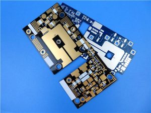
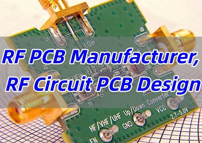
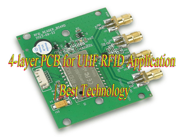
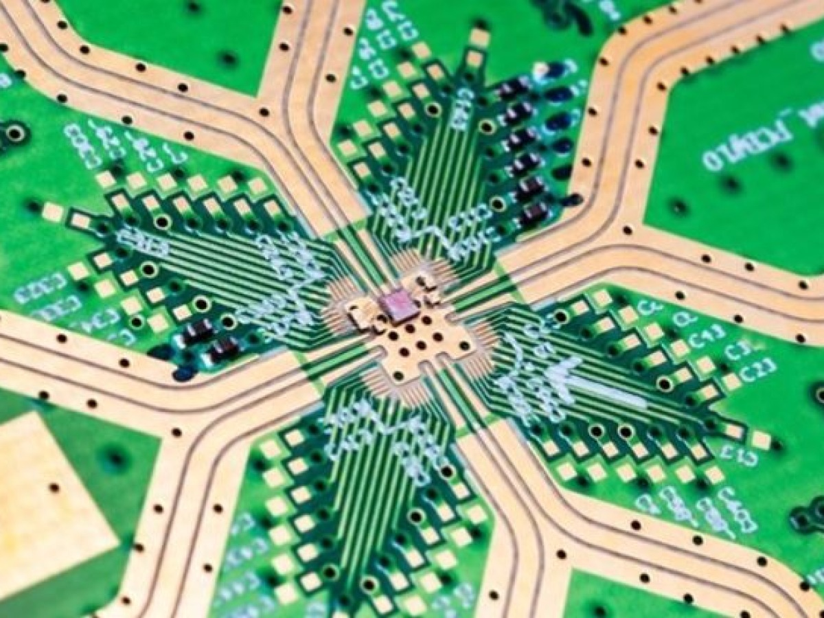
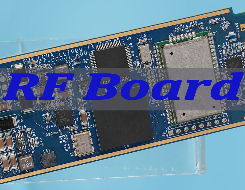
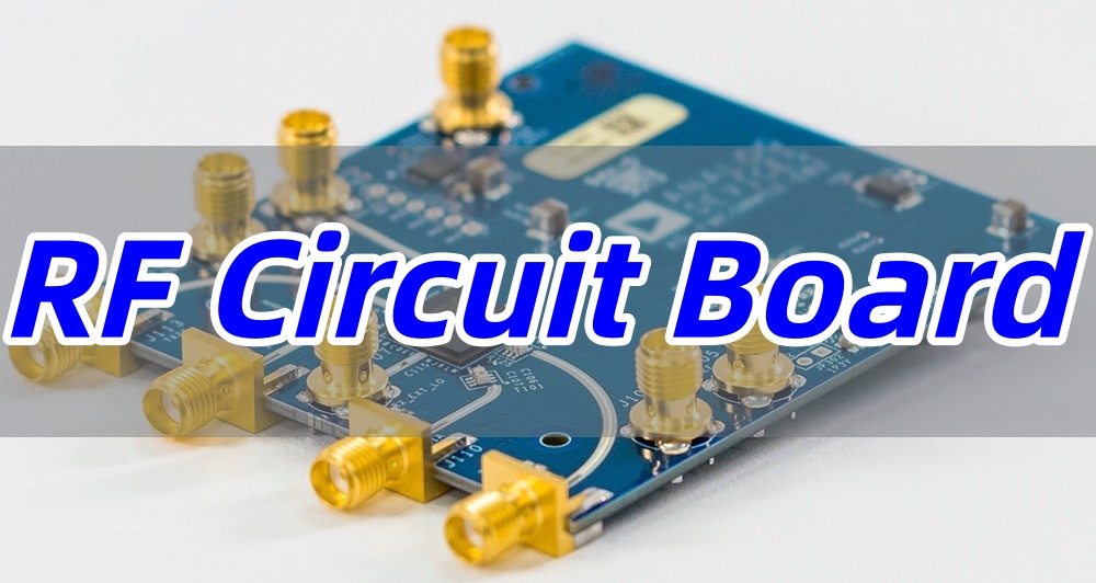
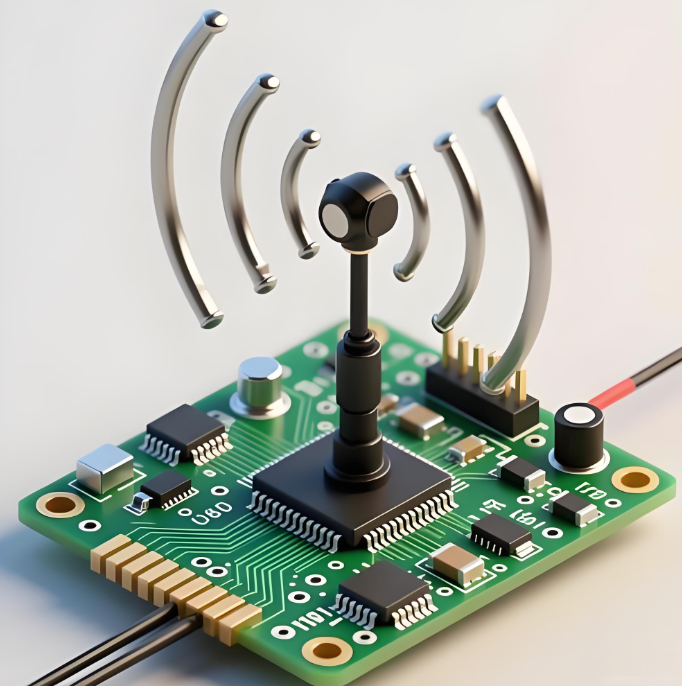
RF PCB work sits at the center of many wireless systems, and an RF PCB often looks similar to a high frequency pcb. Many designers ask if they are the same board. They are related, yet each one handles different needs in signal flow, layout control, and material behavior.

As we move deeper into 5G, radar modules, and clean wireless designs, the differences become more visible. This article explains those differences in simple, clear language. More importantly, it guides engineers, buyers, and project teams on how to choose the right board for their next product.

What Is an RF PCB?

An RF PCB full name is Radio Frequency PCB, which is specifically handles signals in the radio frequency range: typically 300 MHz to 300 GHz, including microwave and millimeter-wave designs.

RF PCBs involve much stricter engineering constraints:

  • Tight impedance (<±5%) on microstrip, grounded CPW, stripline
  • Precise feature control (trace width tolerance around ±0.01–0.03 mm)
  • Stable dielectric properties across temperature
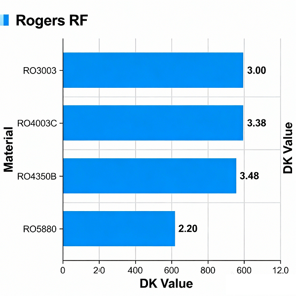
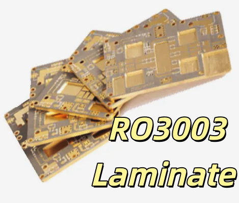
  • Very low-loss materials such as RO3003, RO4350B, RO5880, Taconic RF-35, PTFE woven/non-woven
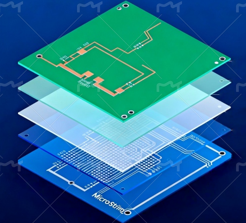
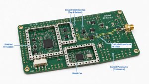
  • Specialized stackups to avoid parasitic radiation
  • Careful via design to avoid stubs and resonance

Applications include:

  • Radar systems
  • Satellite communication
  • LNBs
  • RF front-end modules
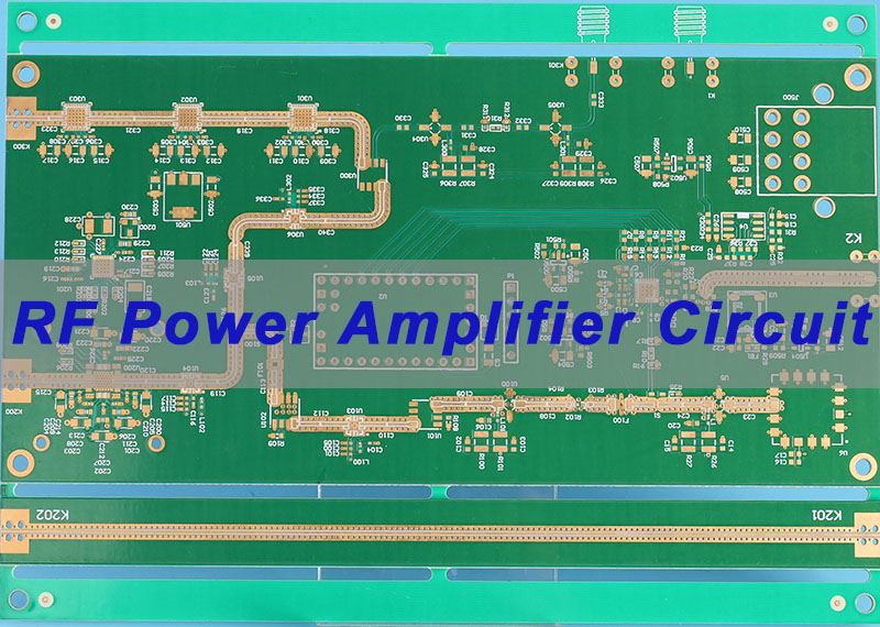
  • Power amplifiers
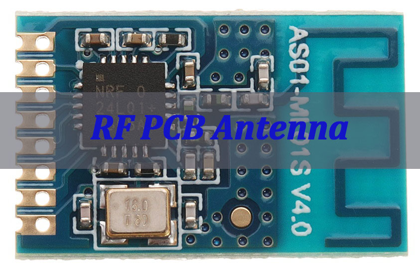
  • Filters, couplers, antennas

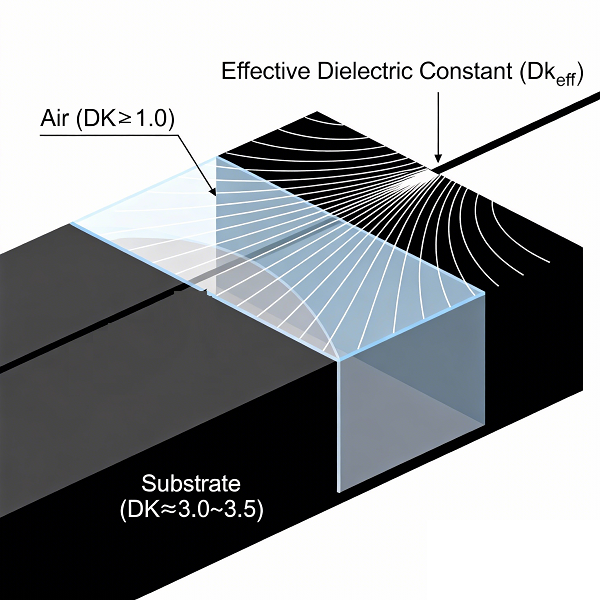
RF PCB is wider use of 5G, IoT, and compact antennas has created strong demand for high-grade rf pcb builds. Because the signals travel along microstrip or CPW structures, the board behaves like part of the RF device, not only a carrier.

What Is a High-Frequency PCB?

A high-frequency PCB is any printed circuit board operating above roughly 500 MHz to 10 GHz+, depending on the design community.

These boards focus on:

  • Stable dielectric constant (Dk tolerance ±0.02–0.05)
  • Low dissipation factor (Df) for reduced signal loss
  • Good impedance control across long traces
  • Suitable materials like Rogers RO4003C, RO4350B, RO3003, PTFE, Isola I-Tera MT40, etc.

High-frequency PCBs serve applications such as:

  • 5G modules
  • Wi-Fi devices
  • GPS receivers
  • High-speed digital layouts (DDR4/DDR5, SerDes)

High frequency boards focus on clean rise times, controlled impedance, and manageable dielectric loss. They support Wi-Fi, Bluetooth, high-speed digital lines, and mixed-signal designs. The design margin is wider than rf pcb work because the board deals with digital pulses, not pure RF energy.

high frequency pcb

High Frequency PCB

Key Differences Between RF PCB vs. High Frequency PCB

AspectHigh-Frequency PCBRF PCB
DefinitionBoards operating at high digital or analog frequenciesBoards designed specifically for RF signal transmission
Signal Range500 MHz–10 GHz+300 MHz–300 GHz
Design FocusSignal integrity, low lossElectromagnetic control, transmission lines, matching
MaterialRogers 4000 series, Isola, Panasonic MegtronPTFE, RO3003/5880, ceramic-filled laminates
Impedance ControlImportantCritical (tighter tolerance)
Manufacturing DifficultyMediumHigh
Typical UseWi-Fi, Bluetooth, high-speed digitalRadar, RF amplifiers, filters, GNSS, mmWave

When Are They “the Same PCB”?

A design can fall under both categories when:

  • The signal is RF (e.g., 2.4 GHz, 5.8 GHz)
  • The designer uses high-frequency materials
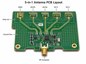
  • The board contains microstrip, CPW, filters, or antennas

For example, a 2.4 GHz RF transceiver board using RO4350B is simultaneously:

  • a high-frequency PCB, because frequency is high
  • an RF PCB, because it processes RF signals

Thus, overlap exists, but they are not inherently identical.

Which One Should You Specify to Your PCB Supplier?

If your project handles RF transmission, always specify RF PCB so the manufacturer focuses on:

  • surface roughness control (Ra < 2 µm for low loss)
  • uniform dielectric thickness
  • controlled resin flow during lamination
  • tighter etching tolerance
  • Dk matching for microstrip/CPW accuracy

If it is only high-speed digital (e.g., PCIe, SerDes), then choose high-frequency PCB.

Why Do RF PCBs Need Special Materials Compared with High Frequency PCBs?

Material behavior influences both categories. Yet an rf pcb is more sensitive to the dielectric constant and copper profile.

RF units run energy through transmission lines. If the copper roughness increases loss, the system sees reduced range or gain shift. If the Dk drifts, the phase response moves. Because of this, the most common materials for rf pcb work include RO3003, RO4350B, RO5880, and PTFE blends.

In contrast, high frequency pcb materials can include Megtron series or Rogers 4000 series because the signal shape is less sensitive to phase stability. They still target low loss, but their working window is wider.

Why Do RF PCBs Need Special Materials Compared with High Frequency PCBs?

What Frequencies Define RF PCB Work vs High Frequency PCB Work?

Both ranges relate to how the signal behaves. RF work usually starts at 300 MHz and goes up to millimeter-wave. This includes radar, satellite, GPS, 24 GHz and 77 GHz systems, and many short-range radios.

High frequency ranges start from about 500 MHz to beyond 10 GHz. These support fast digital buses, Wi-Fi, and mixed-signal designs.

However, the frequency alone does not decide the board’s category. The final system function does.
Do RF PCBs Always Cost More Than High Frequency PCBs?

Actually yes when under the same design. RF boards use premium materials. These materials cost more because they hold stable Dk, low loss, and a smooth copper surface. They also require strict process control during drilling, plating, and lamination.

High frequency boards may use moderate-cost materials such as RO4003C or Megtron 4. They also need controlled lamination, yet the window for yield is wider.

Costs also rise when an rf pcb uses fine lines, tight impedance, or stacked microstrip structures. That said, skilled manufacturers can keep RF costs under control by optimizing stackup and process flow.

What Problems Occur When Designers Use the Wrong PCB Type?

If a design intended for RF is built on a standard high frequency pcb, several issues may appear:

  • Reduced communication range
  • Higher insertion loss
  • Unstable gain
  • Incorrect antenna tuning
  • Phase delay changes
  • EMC issues

Although not every situation is severe, these issues waste time in testing and rework.

When a high frequency digital board is produced using strict RF rules, the design remains stable. Yet the cost often rises without a visible performance gain.

What Tests Are Important for RF PCBs Compared with High Frequency PCBs?

RF boards often need tests beyond regular PCB checks. These include:

  • Dielectric thickness check
  • Dk variation review
  • Copper profile check
  • TDR impedance scan
  • S-parameter review after assembly

High frequency boards may also use TDR scans, yet the tolerance is wider. For RF, every shift affects the final device.

How Does EBest Circuit (Best Technology) Support RF PCB and High Frequency PCB Projects?

EBest Circuit (Best Technology) offers full material guidance, stackup review, transmission line advice, and strong quality assurance for both rf pcb and high frequency pcb builds. We handle small prototype lots and volume orders with the same care. Each rf pcb passes a detailed review, so the final product meets the performance target.

Our strengths include:

  • ISO9001, ISO13485, IATF16949, and AS9100D systems
  • Complete MES traceability
  • Tight impedance control
  • Fine etching for RF lines
  • Skilled process teams for PTFE and hybrid stackups
  • Smooth copper profile management
  • Fast prototype to mass build for global clients

We support antenna work, radar modules, filters, amplifiers, and mixed-signal boards. Our engineering team reviews each design before production to catch layout risks early to speed up product launches. For your next RF or high frequency project, our team stands ready to guide you from concept to delivery!

FAQs

1. Is an rf pcb the same as a high frequency pcb?

No. All RF boards are high frequency boards, but not all high frequency boards meet RF conditions.

2. Can I use RO4003C for both RF and high frequency PCB use?

Yes. However, many RF systems still need lower-loss materials such as RO3003 or RO5880.

3. Are RF boards harder to build?

Yes. They need tighter process control, smoother copper, and stable lamination.

4. How do I know if my design needs an rf pcb?

If your design uses antennas, filters, couplers, or PA modules, you need an RF board.

5. Does EBest Circuit (Best Technology) support RF and high frequency PCBA work?

Yes. We handle full assembly, tuning, connector installation, and testing.

You may also like

RO3003™ PCB Material: Thickness, Datasheet & Cost

December 9th, 2025

Ro3003 is one of the most stable RF laminates used across radar, wireless modules, satellite systems, and mmWave hardware. Ro3003 laminate supports high-frequency designs where low loss and tight impedance matter. Many engineers also use this laminate in sensitive RF blocks where phase stability is critical. In this guide, you will explore ro3003 material in details.

What Is Rogers RO3003 Material?

RO3003™ is a ceramic-filled PTFE laminate developed by Rogers Corporation for high-frequency RF and microwave applications. It offers one of the lowest dielectric loss values available in commercial PCB substrates, making it ideal for 5G, phased-array radar, aerospace communications, and precision antennas.

Key characteristics of RO3003:

  • Ultra-low dielectric constant variation
  • Low dissipation factor for minimal insertion loss
  • Excellent dimensional stability and mechanical consistency
  • Tight dielectric tolerance suitable for phase-critical designs
  • Available in multiple thicknesses for impedance control

RO3003 is part of the Rogers 3000 series, designed specifically for high-frequency, high-reliability RF structures.

RO3003™ PCB Material: Thickness, Datasheet & Cost

Features of Rogers RO3003

RO3003 laminate shows a unique blend of electrical and mechanical traits. These traits make the laminate one of the most trusted RF materials on the market.

  • Stable Dielectric Constant

The dielectric constant stays around 3.00 ± 0.04 at 10 GHz. The tight tolerance helps maintain clean RF transmission lines. This is why many designers use ro3003 controlled impedance structures in radar filters and couplers.

  • Very Low Dissipation Factor

The dissipation factor sits at 0.001 at 10 GHz. Low loss helps preserve signal strength and reduces heating in long RF paths.

  • Low Moisture Absorption

Moisture absorption is around 0.04%. This helps keep the dielectric stable outdoors. It also reduces drift in sensitive antenna circuits.

  • Consistent Mechanical Behavior

RO3003 laminate shows stable CTE values across X, Y, and Z directions. This supports fine-pitch drilling and strong via reliability.

  • Supports High-Frequency Layout

Because of its low loss, ro3003 microwave laminate is a strong fit for 24 GHz sensors, 77 GHz radar, and mmWave imaging.

  • Friendly for Hybrid Stackups

Designers often combine FR4 with ro3003 in a ro3003 hybrid stackup. This helps reduce cost without losing RF performance.

All these features help engineers build stable microwave systems with predictable behavior.

RO3003 Datasheet PDF Technical Overview

Below are the most referenced values from the official RO3003 datasheet:

ParameterTypical Value
Dielectric Constant (Dk 10 GHz)3.00 ±0.04
Dissipation Factor (Df @ 10 GHz)0.0010
Thermal Conductivity0.50 W/m·K
TCDk+3 ppm/°C
Moisture Absorption0.04%
Decomposition Temperature (Td)> 500°C
Density2.1 g/cm³

If you want to know more details about rogers RO3003 laminate datasheet, you can download it at below.

RO3003 Datasheet PDF Technical Overview

Rogers RO3003 Thickness Options

The Rogers RO3003 thickness lineup supports controlled impedance, multilayer RF boards, and antenna substrates:

Common RO3003 Thicknesses (inch/mm):

  • 0.005” (0.13 mm) — (thin radar cores)
  • 0.010” (0.25 mm)
  • 0.015” (0.38 mm)
  • 0.020” (0.50 mm)
  • 0.025” (0.64 mm)
  • 0.030” (0.76 mm) — (stable RF sub-assemblies)
  • 0.060” (1.52 mm) — (antenna, coupler, and filter cores)

Thicker cores enable low-impedance RF lines, while thin cores support fine-pitch microwave structures (filters, couplers).

What Is the Thermal Conductivity of Rogers 3003?

RO3003 thermal conductivity = 0.50 W/m·K

This thermal conductivity is higher than traditional PTFE but lower than hydrocarbon-ceramic materials like RO4350B.

Effectively:

  • Good for moderate-power RF
  • Requires proper heatsinking & via-in-pad for high-power applications

How to Build Stable RF Structures With RO3003 Material?

Designers choose RO3003 material for its strong electrical stability, but the laminate reaches its best performance only when the RF layout follows a strict and systematic approach. The steps below describe how engineers build stable, low-loss, and repeatable RF structures using ro3003 pcb material.

1. Set a Consistent and Accurate RO3003 PCB Stackup

The stackup is the base of every RF design. Before placing any trace, define a stable ro3003 pcb stackup with fixed dielectric thickness and accurate copper weight.

RO3003 has a tight dielectric tolerance, so the main risk comes from variations in laminate thickness. A small shift in the core can move impedance away from your target value.

To avoid this:

  • Pick one RO3003 thickness that matches your controlled impedance goals.
  • Avoid mixing many thickness values in one project unless required.
  • Confirm bonding films if you use a ro3003 hybrid stackup with FR4.

A clean, stable stackup is the first step toward building strong RF structures.

2. Use Copper with Low Roughness for Better High-Frequency Performance

At high frequencies, conductor loss increases as copper becomes rougher. When building a ro3003 microwave laminate design, choose a smoother copper option if your frequency moves above 10 GHz.

For mmWave devices, rolled copper gives better performance than standard ED copper.

Lower copper roughness leads to:

  • Lower insertion loss
  • More stable phase
  • Improved 24 GHz and 77 GHz radar behavior
  • Better antenna radiation when making ro3003 antenna pcb designs

3. Build a Strong Ground Network to Stabilize Return Currents

A tight ground network provides:

  • Lower radiation
  • Lower signal reflection
  • Better matching near connectors
  • Stronger isolation between RF blocks

This is also critical when designing couplers, filters, and antennas on ro3003 pcb material.

4. Keep RF Lines Short, Simple, and Smooth

Shorter RF paths produce lower loss, smooth curves reduce field disturbance and sharp 90° corners create reflections that shift impedance. In a detailed ro3003 pcb design, you should:

  • Use soft bends or chamfered angles
  • Keep trace width uniform along the entire length
  • Avoid necking unless required by components

When traces stay short and smooth, phase stability remains high even in wide-band applications such as 5G or automotive radar.

How to Build Stable RF Structures With RO3003 Material?

5. Reduce Layer Transitions Whenever Possible

In mmWave systems built on ro3003 pcb material, a single via can change the response of a filter or antenna feed. To reduce problems, you can:

  • Keep RF traces on one layer
  • If you must transition, use back drilling
  • Match the pad size to your simulation
  • Surround the via with ground stitching vias

6. Match Connector Pads and Launch Geometry With Simulation

Connector transitions are the most sensitive part of many RF boards. A small mismatch on the connector pad can shift impedance and distort the feed. This is especially true for SMA, SMP, MCX, and UFL connectors.

Rogers RO3003 vs RO4003C vs RO4350B: What are Differences?

PropertyRO3003RO4003CRO4350B
Dk3.003.553.48
Df @ 10 GHz0.0010 (best)0.00270.0037
Thermal Conductivity0.500.710.62
CostHighLowMedium
Max Frequency~40–100 GHz+~10–20 GHz~20–30 GHz
Material BasePTFE ceramicHydrocarbonHydrocarbon
UsageRadar, mmWaveRouters, mid-RFPower RF, telecom

In summary

  • RO3003 → Best for mmWave, radar, precision filters
  • RO4003C → Cost-friendly for mid-RF hardware
  • RO4350B → Good for RF power and backhaul radios

RO3003 is the preferred laminate for high-end millimeter-wave work where small shifts can damage system accuracy.

Popular Usage of RO3003 PCB

RO3003 laminate supports thousands of RF designs. The material functions well in any system where high stability and low loss matter, common usage including:

  • 24 GHz radar modules
  • 77 GHz vehicle radar
  • Point-to-point microwave links
  • Satellite receivers
  • GPS L1/L2/L5 hardware
  • Phased-array antennas
  • RF filters and couplers
  • RF measurement devices
  • mmWave imaging systems
  • High-frequency test boards
  • 5G small cell antennas
  • Imaging systems in security
  • Precision measurement devices
  • Millimeter-wave radar sensors

Many of these designs rely on mmwave ro3003 pcb material for consistent behavior in harsh environments.

Why Rogers 3003 Price Is Higher & How to Reduce It?

Rogers 3003 price is higher than RO4003C or FR-4 because of the PTFE-ceramic system and its strict manufacturing process. PTFE lamination requires special equipment and careful handling. The cost rises due to controlled sintering and slow processing cycles.

You can still lower the overall cost with smart design choices:

1. Use hybrid stack-ups (RO3003 for RF layers + FR-4 for digital layers).

2. Select thinner RO3003 where possible.

3. Optimize panel utilization to reduce waste.

4. Reduce layer transitions

5. Keep traces simple and consistent

6. Minimize layer count.

7. Discuss DFM steps early with the PCB manufacturer.

These steps help reduce cost without losing RF performance.

Fabrication Limits of RO3003 Material

RO3003 can be fabricated well in experienced RF PCB factories, but the material has special requirements.

Typical Fabrication Limits

ParameterTypical Limit
Minimum trace width3 mil (depends on copper)
Minimum spacing3 mil
Plated through-hole size≥0.2 mm
Laser microviaYes, but PTFE drilling needs caution
Hybrid laminationPossible with bonding layers
Solder maskControlled to avoid impedance shift
Tolerance±10% or better for RF lines

RO3003 PCB Layout Design Tips

  • Keep RF lines straight
  • Use smooth bends, not sharp corners
  • Place ground stitching close to key lines
  • Keep distance between RF and digital areas
  • Use stable reference planes
  • Match connector pads with simulation results
  • Use isolation areas between sensitive blocks

Frequently Asked Questions About RO3003

1. Does RO3003 support mmWave?

Yes. Many mmwave ro3003 pcb systems use it at 24 GHz and 77 GHz.

2. Can RO3003 be mixed with FR4?

Yes. Designers use it in a ro3003 hybrid stackup to reduce cost.

3. Why is RO3003 expensive?

PTFE processing and ceramic filler raise the cost.

4. What is the loss tangent?

The loss tangent is 0.001 at 10 GHz.

5. Can RO3003 be used for antennas?

Yes. Its stable dielectric supports precise antennas.

Why Choose EBest Circuit (Best Technology) for RO3003 PCB Manufacturing?

RO3003 supports advanced RF structures where stability, low loss, and tight impedance are important. To reach the laminate’s full performance, you need a manufacturer with strong PTFE skills. EBest Circuit (Best Technology) offers stable fabrication lines, SI9000 modeling, clean etching control, and strict lamination parameters. We also hold ISO9001, ISO13485, IATF16949, and AS9100D certifications for high-reliability hardware.

We support ro3003 pcb fabrication, ro3003 hybrid stackup builds, radar module assembly, antenna PCBA, and full RF tuning. Our engineering team reviews your layout, stackup, and fabrication notes to help lower ro3003 pcb cost and improve long-term performance.

You may also like

Rogers RO3003 Laminate Datasheet Detailed Explaination

December 8th, 2025

RO3003 is widely used across RF and microwave PCB because it offers stable electrical behavior, low loss, and smooth processing on modern PCB lines. Engineers often choose this laminate when they need predictable impedance, steady phase response, and strong thermal performance at high frequencies. Below is a comprehensive, fabrication-level RO3003 datasheet, covering electrical, mechanical, thermal, chemical, processing, and reliability properties.

Rogers RO3003 Laminate Datasheet Detailed Explaination

Rogers RO3003 Laminate Datasheet

Rogers RO3003™ Electrical Properties

ParameterConditionTypical ValueNotes
Dielectric Constant (Dk)10 GHz (IPC-TM-650 2.5.5.5)3.00 ± 0.04Very stable across temperature and frequency
Dielectric Constant (Dk)2.5 GHz3.01Suitable for wideband RF
Dissipation Factor (Df)10 GHz0.0010Extremely low loss
Dissipation Factor (Df)2.5 GHz0.0009Excellent for mmWave
Volume Resistivity23°C / 50% RH1.7 × 10¹⁰ MΩ·cmHigh electrical insulation
Surface Resistivity23°C / 50% RH5.7 × 10⁹ MΩStable in damp conditions
Electric Strength0.5 mm thickness35 kV/mmStrong dielectric barrier
Impedance Stability-40°C to +85°C±1.3%Very stable for antenna structures
Dk Temperature Coefficient (TCDk)-40 to +85°C-3 ppm/°CVery low drift

RO3003 is chosen often for 77 GHz radar, 24 GHz radar, and mmWave antennas because of these stable dielectric properties.

RO3003™ Material Thermal Properties

ParameterTypical ValueNotes
Thermal Conductivity0.5 W/m·KHigher than FR4
Usable Temperature Range-55°C to +150°CSuitable for automotive radar
Dimensional Stability (X/Y)0.2–0.3%Strong laminate stability
Coefficient of Thermal Expansion (CTE) – X17 ppm/°CMatches copper closely
CTE – Y17 ppm/°CHelps reduce expansion stress
CTE – Z24 ppm/°CCritical for microvias
Thermal Decomposition Temp (Td)> 400°CMuch higher than FR4
Thermal Stress288°C / 10 secNo delamination
Specific Heat1.0 J/g-KSupports stable power handling

The matched X/Y CTE and moderate Z-axis CTE improve reliability in multi-layer RF boards, QFN modules, and BGA transitions.

RO3003™ Mechanical Properties

ParameterConditionTypical Value
Tensile Modulus (MD)23°C18,000 MPa
Tensile Modulus (CD)23°C17,500 MPa
Flexural Strength23°C340 MPa
Peel Strength1 oz Cu, after thermal aging8.0 lb/in
Density2.1 g/cm³
Hardness (Shore D)74
Moisture Absorption48h @ 50°C water0.02%

Low moisture absorption is one of the main reasons designers choose Ro3003 laminate for outdoor and long-range radio systems.

RO3003™ Chemical & Environmental Properties

PropertyTypical Value
FlammabilityUL 94 V-0
Fungus ResistancePass
Copper Corrosion TestPass
Water Absorption0.02%
RoHSCompliant
Lead-Free AssemblyFully supported

The laminate performs well in harsh environments such as marine radar, industrial sensors, and automotive radar systems.

RO3003™ Thickness Availability

Standard ThicknessInchesMilNotes
0.127 mm0.0050″5 milVery common for antennas
0.203 mm0.0080″8 milGood for compact RF paths
0.254 mm0.0100″10 milLNA/PA front-end boards
0.508 mm0.0200″20 milMany GPS modules
0.762 mm0.0300″30 milLower insertion loss
1.524 mm0.0600″60 milLarge antennas or radar

Copper foil options include:

Copper TypeStandard WeightNotes
ED Copper½ oz, 1 ozBest for general RF
Reverse-Treat Copper (RTF)½ oz, 1 ozBetter for low-loss designs
Rolled CopperLimitedUsed for bending applications

RO3003™ Available Panel Sizes

Panel SizeNotes
12″ × 18″Most common
18″ × 24″Higher utilization
24″ × 36″For mass production
Custom CutsBy manufacturer

Panel selection strongly affects Rogers 3003 price because utilization changes final cost.

RO3003™ Impedance Control Data

Line TypeResult on 10 mil RO3003Notes
50 Ω Microstrip~23 mil widthTypical, depends on copper
75 Ω Microstrip~12 mil widthUsed in satellite links
100 Ω Differential Pair8–10 mil / 8–10 mil spacingDepends on copper thickness
90 Ω Diff Pair10–12 milCommon in RF front ends

For mmWave (60–86 GHz), designers often use:

FeatureTypical Value
Via Stub Target< 6 mil
CPWG Gap6–8 mil
BendsAvoid sharp angles

RO3003™ Reliability Properties

TestResult
Thermal CyclingExcellent stability
IST TestLow via fatigue
PTH ReliabilityStable with standard processes
Solder FloatNo blistering
High-Temp ExposureNo resin cracking
Multi-Reflow TestStable after 3× lead-free reflow

RO3003 is widely used in 77 GHz automotive radar because it withstands large temperature swings without drift.

RO3003™ Comparison Against Other Rogers Materials

ParameterRO3003RO4003CRO4350B
Dk3.003.383.48
Df0.00100.00270.0037
Moisture Absorption0.02%0.04%0.06%
Thermal Conductivity0.5 W/m·K0.3 W/m·K0.6 W/m·K
Dimensional StabilityHighMediumHigh
Fabrication DifficultyLowVery lowLow
CostHighestLowestMedium
Best ForRadar, mmWaveGeneral RFTelecom, WiFi, RF modules

RO3003™ Material Stack-Up Examples

  • 1- Layer RF Antenna Stack-Up
LayerMaterial
Top Copper18 μm RTF
DielectricRO3003 10 mil
Ground Copper18 μm RTF
  • 2-Layer Balanced RF Module
LayerMaterial
Signal Layer½ oz copper
RO3003 Core20 mil
Ground Layer1 oz copper
  • Hybrid RF + Digital Stack-Up
LayerMaterial
Top CopperRF traces
RO300310 mil
Adhesive Layer
FR4 PrepregStandard
FR4 CoreDigital circuits
Bottom CopperGround / digital signals

If your next RF project involves RO3003 or other high-frequency laminates, our engineering team is ready to assist with simulations, stack-up proposals, prototype runs, and volume builds. You are welcome to contact EBest Circuit (Best Technology) for professional guidance and fast support as you move from concept to production.

Our teams support RF designers from the early stack-up stage through final production with careful engineering review, material guidance, and precise process control. Every PCB moves through certified systems, including ISO9001, ISO13485, IATF16949, and AS9100D, which gives customers confidence in long-term reliability.

You may also like

Premium HDI RF Board for Reliable High-Frequency Designs

December 8th, 2025

An HDI RF Board is a sophisticated printed circuit board that merges High-Density Interconnect technology with specialized materials and design rules to excel in radio frequency applications. Pushing the limits of modern wireless, radar, and sensing systems demands circuits that are faster, smaller, and more reliable than ever. This article provides a comprehensive guide to understanding HDI RF boards, their advantages for high-frequency designs, key structural elements, cost considerations, comparisons with other substrates, and guidance on selecting a reliable HDI PCB manufacturer.

Are your current PCB solutions holding back your next-generation RF design? You might be facing these common challenges:

  • Signal Degradation at High Frequencies:​ Standard PCB constructions struggle with significant signal loss, crosstalk, and impedance discontinuities, crippling the performance of sensitive RF and microwave circuits.
  • Size and Weight Constraints:​ Achieving complex functionality often means larger, multilayer boards that contradict the miniaturization goals of modern portable and aerospace electronics.
  • Thermal Management Headaches:​ Dense component placement and high-power RF sections generate concentrated heat that standard boards cannot effectively dissipate, leading to reliability risks.
  • Prototyping and Yield Frustrations:​ Complex RF designs often require multiple expensive prototype iterations, and manufacturing defects in fine features can lead to poor yield and project delays.
  • Supply Chain and Expertise Gaps:​ Finding a manufacturer with both advanced HDI technology in PCB​ fabrication and deep RF/microwave​ design support is difficult, leading to communication breakdowns and suboptimal results.

The solution lies in partnering with a specialist who masters the fusion of HDI fabrication and RF principles. At BEST Technology, we engineer Premium HDI RF Boards​ specifically to overcome these hurdles.

  • Superior Signal Integrity:​ We utilize advanced HDI layer​ stacking, low-loss materials, and precise impedance control to ensure clean, high-fidelity signal transmission for your RF and microwave circuit boards.
  • Enabled Miniaturization:​ Our expertise in microvias and fine-line patterning packs more functionality into a smaller footprint, crucial for compact HDI Electronics​ and antenna systems.
  • Enhanced Thermal & Mechanical Reliability:​ We integrate thermal management strategies and robust stack-up designs from the start, ensuring your board remains stable and reliable under operational stress.
  • DFM-Driven Process & High Yield:​ Our design-for-manufacturability review and controlled processes reduce prototyping cycles and ensure high production yield, even for complex designs like HF RFID antenna​ modules.
  • One-Stop Expert Partnership:​ As a leading HDI RF Board manufacturer, EBest Circuit (Best Technology) provides end-to-end support—from material selection and design review to advanced fabrication and testing—simplifying your supply chain.

BEST Technology is a premier specialist in manufacturing advanced printed circuit boards, with over 19 years of expertise in HDI PCB​ and high-frequency solutions. We combine state-of-the-art production facilities with profound technical knowledge to serve clients in telecommunications, aerospace, defense, and medical industries. We are not just a HDI PCB manufacturer; we are your technical partner in realizing cutting-edge HDI RF​ designs and solutions. For inquiries, pls feel free to contact us at sales@bestpcbs.com.

HDI RF Board

What Is an HDI RF Board?

At its core, an HDI RF Board is defined by the application of High-Density Interconnect (HDI) methodologies to boards operating at radio frequencies. To understand the HDI PCB definition, it is a board with a higher wiring density per unit area than conventional PCBs, achieved through features like microvias (laser-drilled), fine lines and spaces, and sequential lamination. When this is applied to RF designs, it involves using specialized low-loss laminate materials (like Rogers, Taconic) alongside these HDI techniques.

How HDI RF Circuit Board Differs from Standard High-Frequency Designs? Here’s how it differs from standard RF boards:

  • Interconnect Density:​ Standard RF boards often use larger through-hole vias, limiting routing space. HDI RF boards employ microvias (often blind and buried), allowing escape routing from dense RF ICs (like BGAs) and more efficient layer transitions.
  • Material Integration:​ While both may use similar high-frequency laminates, HDI RF boards require materials that are also compatible with the multiple lamination cycles and fine-feature etching of HDI processes.
  • Design for Performance and Size:​ A standard design might increase board size to accommodate components and routing. An HDI RF design optimizes both electrical performance (shorter, controlled paths) and physical size simultaneously.
  • Manufacturing Complexity:​ The fabrication of HDI RF boards is significantly more complex, requiring precise control over dielectric thickness, via formation, and copper profiling to maintain consistent RF characteristics.

In summary, an HDI RF board is the strategic convergence of miniaturization technology (HDI) and high-frequency engineering, creating a platform that is superior for modern, compact, and high-performance wireless devices.

HDI RF Board

Why HDI Technology in PCB Matters for RF Performance?

The role of HDI technology in PCB​ fabrication is transformative for RF applications. It directly addresses the critical demands of high-frequency circuits.

  • Minimized Signal Path Length:​ Shorter traces between components, enabled by dense interconnects, reduce signal delay, propagation loss, and the chance of picking up noise.
  • Improved Impedance Control & Signal Integrity:​ The fine-line capabilities of HDI allow for precise control over trace width and spacing, which is paramount for maintaining consistent characteristic impedance (e.g., 50Ω) across the board, minimizing reflections.
  • Reduced Parasitic Effects:​ Microvias have lower parasitic capacitance and inductance compared to traditional through-hole vias. This is crucial at GHz frequencies, where via stubs can act as antennas or cause resonances.
  • Enhanced Grounding and Shielding:​ Multiple buried vias can create a dense via fence or a coaxial-like shielding structure around sensitive RF lines, effectively containing electromagnetic interference (EMI) and crosstalk.
  • Facilitation of Advanced Packaging:​ HDI is essential for integrating embedded passive components (resistors, capacitors) and for fan-out routing from advanced semiconductor packages, keeping the entire RF front-end compact and efficient.

For RF performance, HDI is not just about making the board smaller; it’s about making it electrically superior by reducing negative effects intrinsic to larger, conventional geometries.

Key Structure and HDI Layer Configurations Used in Advanced RF Modules and Antenna Systems

The architecture of an HDI RF board is its blueprint for success. The HDI layer​ build-up is carefully planned to meet electrical and mechanical goals.

  • Standard “1+N+1” to “Any Layer” Build-Ups:​ Simple HDI starts with “1+N+1” (one HDI layer on each side of a core). Advanced RF modules may use “2+N+2” or “any layer” HDI, where almost every layer can be connected with microvias, offering maximum design flexibility for complex HDI Electronics.
  • Hybrid Material Stack-ups:​ A common configuration uses a high-performance, low-loss RF laminate (e.g., Rogers 4350B) for critical signal layers, bonded with standard FR-4 prepreg for other layers. This optimizes cost and performance.
  • Buried and Blind Via Structures:​ Critical RF lines often reside on outer layers for best performance. Blind vias connect surface layers to adjacent inner layers without going through the entire board, preserving space and reducing stub length.
  • Via-in-Pad and Filled Vias:​ To further miniaturize, vias are placed directly in component pads. These are plated and filled with conductive or non-conductive material, creating a flat surface for soldering and excellent thermal conduction for components like power amplifiers.
  • Shielding Cavities and Antenna Structures:​ HDI processes can create milled cavities for shielding cans or precise, multi-layer antenna structures like patch antennas for HF RFID antenna​ systems, all integrated within the board itself.

This sophisticated layering is what allows a single, compact HDI RF Board​ to function as an entire RF subsystem.

What is HDI RF Board Price?

The HDI RF board price​ is not a fixed number but a variable determined by a confluence of technical factors. Understanding these helps in budgeting and design optimization.

  • Board Complexity:​ This is the primary driver. More sequential lamination cycles, a higher count of laser-drilled microvias, and “any layer” capability increase cost significantly.
  • Material Selection:​ High-frequency laminates (Rogers, Taconic, etc.) are far more expensive than standard FR-4. The percentage of these materials in the hybrid stack-up directly impacts the raw board cost.
  • Layer Count and Size:​ More layers and a larger board area naturally increase material and processing time. HDI allows for smaller sizes, which can offset the cost of increased layer count.
  • Specialized Processes:​ Costs for via-in-pad, filled vias, tight impedance control tolerances (e.g., ±5%), and advanced surface finishes (ENEPIG) add to the final price.
  • Order Volume and Turnaround Time:​ Prototype quantities have a higher cost per unit. Production volumes bring economies of scale. Expedited fabrication also carries a premium.

As a rough guideline, expect an HDI RF board to cost 2 to 5 times more​ than a standard FR-4 PCB with the same dimensions and layer count, primarily due to materials and process complexity. The investment, however, is justified by the unparalleled performance and integration it enables.

Comparing HDI Electronics with Flex PCB, LED PCB, and Other Specialized Substrates for RF Applications

Choosing the right substrate is critical. Here’s how HDI Electronics​ compare:

  • HDI RF Board vs. Flex PCB:​ Flex boards offer dynamic bending and space savings in assemblies. However, for core RF circuitry, standard flex materials often have higher loss tangents. HDI rigid boards provide better rigidity for component support, superior thermal management, and wider availability of ultra-low-loss laminate options. They are often used together (Rigid-Flex) where HDI areas handle the core RF processing.
  • HDI RF Board vs. Standard LED PCB:​ A typical LED PCB​ prioritizes high thermal conductivity (using metal core like Aluminum) and simple circuitry to drive LEDs. An HDI RF board is focused on signal integrity at high frequencies, using different materials and complex, controlled-impedance routing. Their purposes are distinct.
  • HDI RF Board vs. Standard FR-4 Multilayer:​ Standard multilayer boards lack the fine features and low-loss materials. They are unsuitable for high-frequency performance but are cost-effective for digital and low-frequency analog sections. HDI RF is the specialized choice for the RF front-end.
  • HDI RF Board vs. Pure Ceramic Substrate (e.g., Alumina, LTCC):Ceramic offers excellent thermal performance and very fine features but at a very high cost and limited size. HDI RF on organic laminates provides a better balance of performance, size, design flexibility, and cost for most RF applications below the millimeter-wave extreme.

In essence, for the heart of a high-frequency system—where signal integrity, miniaturization, and integration are non-negotiable—the Premium HDI RF Board​ is the unmatched solution.

How HF RFID Antenna, RFI Board, and RDI Board Designs Benefit from HDI Technology?

These specialized applications gain distinct advantages:

  • HF RFID Antenna:​ It is short for High Frequency Radio Frequency Identification Antenna. HF RFID antenna​ coils often require precise, multi-turn patterns. HDI technology allows these coils to be fabricated with extreme accuracy as embedded planar structures within the board layers, improving reliability and enabling integration with the control chip in a single, slim package.
    Application: Operating at the 13.56 MHz HF band, these HDI-enabled antenna inlays or modules are critical for contactless payment systems (e.g., credit cards, mobile wallets), secure access control badges, library item tracking, and high-security document authentication.
  • RFI (Radio Frequency Interference) Board:​ Boards designed to mitigate RFI​ need excellent shielding. HDI allows for the easy creation of dense ground via fences and shielded cavities between noisy and sensitive sections directly within the board structure, providing superior isolation compared to external shields.
    Application: Crucial for applications across a wide frequency spectrum, these boards are used in sensitive medical imaging equipment (MRI), high-density telecom infrastructure, aerospace avionics, and advanced test & measurement instruments to prevent signal degradation and ensure regulatory EMI/EMC compliance.
  • RDI (Research, Development, and Innovation) Boards:Prototype and RDI board​ projects for cutting-edge technology benefit immensely from HDI’s flexibility. It allows researchers to pack sensors, RF components, and digital processors into a small form factor for proof-of-concept devices, accelerating innovation cycles.
    Application: :​ Used in prototyping next-generation IoT devices, millimeter-wave (mmWave) communication systems (e.g., 5G/6G fronthaul), phased array radar elements, and quantum computing interfaces, where form factor, signal integrity, and rapid design iteration are paramount.

In all cases, HDI provides the design freedom and performance consistency needed to turn advanced concepts into reliable, manufacturable products.

How to Select Reliable HDI RF Board Manufacturers?

Choosing the right partner is as important as the design itself. Look for these traits in HDI RF board manufacturers:

  • Proven Technical Expertise:​ They must demonstrate a deep understanding of both HDI processes and RF principles (impedance, loss, materials).
  • Advanced Manufacturing Capability:​ Verify they have laser drilling, precision lamination, and electrical testing equipment (like network analyzers) specifically for RF parameters.
  • Material Partnerships:​ Access to a wide range of certified high-frequency laminates from leading suppliers is essential.
  • Design Support Services:​ The best manufacturers offer upfront engineering support, including stack-up design, simulation assistance, and thorough DFM analysis.
  • Quality and Certifications:​ Look for relevant industry certifications (ISO, IATF 16949, AS9100 for aerospace) and a robust quality management system.
HDI RF Board

Why Choose BEST Technology as One of Your Best HDI PCB Manufacturers for RF and Microwave Circuit Boards?

BEST Technology stands out by fulfilling all the above criteria and more. We specialize in the niche intersection of HDI and high-frequency, offering:

  • Dual Expertise:​ Our engineers are fluent in the language of both advanced fabrication and RF design.
  • State-of-the-Art Facility:​ Equipped with specialized lines for handling low-loss materials and achieving tight tolerances.
  • End-to-End Partnership:​ We collaborate from the early design stage through prototyping to volume production, ensuring your RF and microwave circuit boards​ are not only designed well but are also optimized for manufacturability and yield.
  • Commitment to Reliability:​ Every Premium HDI RF Board​ we build undergoes rigorous testing to meet the stringent requirements of high-reliability applications. And our PCB and SMT factory is fully compatible with ISO 9001, ISO 13485, IATF 16949, AS9100D, UL, REACH, and RoHS.
  • Short Lead Times: We operate dedicated, streamlined production lines and maintain strategic raw material partnerships. This optimized workflow, combined with our deep process expertise, allows us to offer industry-leading turnaround times for both complex prototypes and volume production, enabling you to accelerate your product development and meet critical market windows without compromising on quality.
HDI RF Board

All in all, an HDI RF Board​ represents the pinnacle of integration for high-frequency electronics, combining the miniaturization power of HDI with the performance demands of RF circuits. This guide has explored its HDI PCB definition, benefits, structures, costs, and ideal applications to help you leverage this advanced technology for your most demanding projects.

Success in this field requires a manufacturer that is more than a fabrication house; it requires a technical co-innovator. BEST Technology brings nearly two decades of specialized HDI RF circuit board experience, cutting-edge capabilities, and a partnership-driven approach to every HDI device project. Pls feel free to contact us for a consultation or quote via sales@bestpcbs.com

FAQs

Q: What is the difference between HDI PCB and regular PCB?

  • A: The main differences are density and construction. HDI PCBs use microvias (typically <150µm), finer traces/spaces, and often sequential build-up to achieve much higher interconnection density in a smaller area compared to regular PCBs that rely on larger through-hole vias and simpler lamination.

Q: What are the benefits of HDI PCB?

  • A: Key benefits include significant size and weight reduction, improved electrical performance (faster signals, less noise), enhanced reliability (fewer mechanical interconnections), and the ability to accommodate advanced, high-pin-count components like BGAs.

Q: What are the 4 tiers of HDI?

A: HDI complexity is often categorized into tiers:

  • Tier 1:​ 1+N+1 (Microvias on one side of the core).
  • Tier 2:​ 2+N+2 (Microvias on both sides, potentially with stacked vias).
  • Tier 3:​ 3+N+3 (Multiple layers of stacked microvias).
  • Tier 4 & Above:​ Also called “Any Layer” HDI, where microvias can connect any two adjacent layers throughout the board stack-up.

Q: What is the process of HDI PCB fabrication?

  • A: It involves sequential lamination cycles. Key steps include: imaging and etching of fine inner layers, laser drilling of microvias, via metallization (plating), layer alignment and bonding (lamination), and repeat. This differs from standard PCB fab which often uses a single lamination of all layers followed by mechanical drilling of through-holes.

Q: What is an HDI device?

  • A: In the context of PCBs, an “HDI device” typically refers to the final electronic product or module that is enabled by or built upon an HDI printed circuit board, such as a smartphone, a satellite communication module, or a medical imaging device.

You may also like

Rogers RO4350B Datasheet & Material Guide for RF PCB Designers

December 5th, 2025

If you are working on RF or microwave PCB design, the material you choose directly impacts signal loss, phase stability, thermal performance, and overall system reliability. Rogers RO4350B is one of the most widely used high-frequency laminates in telecom, radar, 5G, satellite, and advanced wireless systems. This guide provides a complete breakdown of RO4350B datasheet properties, thickness options, RF advantages, and a comparison against FR4—plus practical manufacturing notes for PCB engineers.

What Is Rogers RO4350B Material?

Rogers RO4350B is a hydrocarbon-ceramic, glass-reinforced laminate engineered for RF and microwave applications from the Rogers RO4000® series. Unlike PTFE-based laminates, RO4350B can be fabricated using standard FR4 PCB processes—a huge benefit for cost, lead time, and manufacturability—while still delivering excellent electrical stability at GHz frequencies.

Key characteristics:

  • Dk = 3.48 ± 0.05 (10 GHz, z-axis)
  • Df ≈ 0.0037 (low loss)
  • High thermal stability
  • Low moisture absorption (<0.06%)
  • Compatible with FR4 processes
  • Excellent for hybrid stack-ups
Rogers RO4350B Datasheet & Material Guide for RF PCB Designers

What Is Rogers RO4350B Material?

What Is RO4350B Used for in RF PCB Applications?

RO4350B is found in nearly every modern RF system. Typical uses include:

  • 5G antennas and base-stations
  • Phased-array radar modules
  • LNA, PA, and front-end RF chains
  • Power amplifiers requiring robust thermal paths
  • Filters, couplers, baluns, and RF matching networks
  • Automotive ADAS radar
  • Satellite communication modules
  • High-performance mixed-signal and RF/digital hybrid boards

Because it balances cost and performance, RO4350B is ideal for mid-to-high volume RF production.

Rogers RO4350B Datasheet: Full Material Properties Overview

Below is a consolidated summary of all essential RO4350B datasheet values RF engineers frequently use in simulation, stack-ups, and manufacturing notes.

RO4350B Electrical Properties

PropertyTypical ValueTest Condition / Notes
Dielectric Constant (Dk)3.48Measured at 10 GHz
Dielectric Constant Stability±0.05Across thickness range
Dk Temperature Coefficient+50 ppm/°C−50°C to +150°C
Dissipation Factor (Df)0.0037@ 10 GHz
Volume Resistivity1×10⁷ MΩ·cmASTM D257
Surface Resistivity1×10⁷ MΩASTM D257
Dielectric Strength40 kV/mmTypical
Electrical Loss StabilityExcellentWideband RF use

RO4350B Thermal Properties

PropertyTypical ValueNotes
Thermal Conductivity0.69 W/m·KSupports heat-spreading features
Tg (Glass Transition Temperature)>280°CVery stable for lead-free
Td (Decomposition Temperature)≈390°CRogers method
CTE (X-axis)11 ppm/°CStrong dimensional stability
CTE (Y-axis)14 ppm/°CGood panel reliability
CTE (Z-axis)32 ppm/°CSupports plated through-hole reliability
T260 Time>60 minAnti-delamination performance
T288 Time>20 minHigh thermal endurance

RO4350B Copper Options

Copper TypeThicknessNotes
Rolled Copper½ oz, 1 ozBetter for low-loss RF lines
Electrolytic Copper½ oz, 1 oz, 2 ozStandard PCB production
Reverse-Treated CopperAvailableImproved adhesion in hybrid stack-ups

For more details about Rogers RO4350B, click here: Rogers RO4350B Datasheet Download

RO4350B Thermal Conductivity

RO4350B’s thermal conductivity of 0.69 W/m·K is significantly higher than typical FR4 (~0.3 W/m·K).

This means:

  • Better heat spreading
  • Higher reliability under RF power loads
  • Improved board life during thermal cycles
  • Lower risk of delamination

This makes RO4350B a strong candidate for RF power amplifiers and modules with high current density.

RO4350B Thickness Options & Common Stack-Up Selections

RO4350B thickness availability is wide, giving designers flexibility.

Common RO4350B Thicknesses

  • 0.101 mm / 0.004”
  • 0.203 mm / 0.008”
  • 0.254 mm / 0.010”
  • 0.3048 mm / 0.012”
  • 0.406 mm / 0.016”
  • 0.508 mm / 0.020”
  • 0.813 mm / 0.032”
  • 1.524 mm / 0.060”

Copper options: ½ oz, 1 oz, 2 oz.

Common Stack-up Approaches

1. RF-only board:

Single RO4350B core for antennas, filters, or couplers.

2. Hybrid stack-up (RO4350B + FR4):

  • RF layers on RO4350B
  • Digital/Power layers on FR4
  • Best cost-performance balance

3. Multilayer RO4350B stack-up:

For radar, high-power, or mmWave systems requiring uniform RF behavior.

RO4350B vs FR-4: Differences in RF Performance

FR-4 is a good general-purpose material but struggles at higher RF bands. Its dielectric constant shifts with humidity, temperature, and frequency. Loss levels rise significantly above 1–2 GHz, which affects range, efficiency, and signal clarity.

RO4350B addresses these issues with stable electrical behavior, low loss, and stronger control of impedance.

FeatureRO4350BFR-4
Dk StabilityVery stableUnstable at high frequency
Loss (Df)LowHigh
High-frequency useExcellentLimited
Thermal stabilityStrongModerate
RF performanceConsistentVaries widely
Typical useRF, microwave, antennasGeneral electronics

For RF paths, RO4350B is nearly always the better choice.

Rogers 4000 Series Materials Overview

The RO4000® series includes hydrocarbon-ceramic laminates designed for RF and microwave work. The series offers stable dielectric values, low moisture absorption, and predictable performance across frequency ranges. These materials support antennas, filters, couplers, radar units, medical sensors, and industrial communication systems. RO4003C and RO4350B are the most common choices, though other variants exist for special electrical or mechanical needs. Here are some other RO4000® series materials:

Rogers 4000 Series Materials Overview

Which Rogers Materials Can Be Used for RF & Microwave PCB?

Common Rogers RF materials include:

  • RO4350B – balanced performance, processable like FR4
  • RO4003C – lower loss, great for 10+ GHz
  • RO4835 – improved oxidation resistance and stability
  • RT/duroid® series – PTFE-based ultra-low-loss materials for mmWave
  • TMM® series – ceramic thermoset laminates for precision high-power RF

Choose based on frequency, thermal load, and tolerance requirements.

RO4350B PCB Manufacturing Considerations

Although RO4350B is easier to manufacture than PTFE materials, achieving consistent RF performance requires following specific process guidelines. Here are the key considerations for PCB fabrication:

RO4350B PCB Manufacturing Considerations

RO4350B PCB Manufacturing Considerations

1. FR4-compatible processing, but with controlled parameters

RO4350B supports standard PCB processes, but drill speeds, lamination pressure, bake profiles, and final copper thickness must be carefully controlled to ensure stable impedance and dielectric consistency.

2. Hybrid stack-ups require expert lamination control

When combining RO4350B with FR4, differences in CTE (coefficient of thermal expansion) must be managed to avoid warpage, resin starvation, or delamination. Precise prepreg selection and lamination cycles are essential.

3. Accurate impedance control is critical

RF designs often require ±5% or tighter impedance tolerance. Manufacturers must account for:

  • dielectric thickness tolerance
  • copper roughness
  • resin-filled vias or back-drilling
  • line-width compensation

Providing simulation models or stack-up notes (Dk/Df @ frequency) helps ensure fabrication accuracy.

4. Drilling & plating demands tighter control

RO4350B’s ceramic-filled structure requires optimized drill parameters to prevent smear and maintain high hole-wall quality, ensuring reliable via plating for multilayer RF PCBs.

5. Proper material storage and handling

To prevent moisture absorption and dimensional shift, the material should be kept in a dry, controlled environment and baked before lamination when necessary.
With these practices, RO4350B PCBs can achieve repeatable RF performance from prototype to mass production.

Why EBest Circuit (Best Technology) Is Preferred for RO4350B PCB Fabrication?

When working with RO4350B, choosing the right PCB manufacturer is critical. EBest Circuit (Best Technology) is trusted by RF engineers because:

  • They stock RO4350B in multiple thicknesses
  • Provide RF stack-up simulation support
  • Offer tight impedance control with test coupons
  • Perform high-precision routing and controlled-depth milling
  • Support hybrid RO4350B + FR4 multilayers
  • Provide material certifications and Rogers-lot traceability

If you need consistent RF performance from prototype to mass production, EBest Circuit (Best Technology) is a reliable partner for RO4350B PCB fabrication.

FAQs

1. Does RO4350B support buried or blind vias in multilayer RF boards?

Yes. RO4350B works well in multilayer designs that use blind or buried vias. Its mechanical strength and low z-axis expansion help maintain via reliability during lamination and thermal cycling. When designers use selective RO4350B layers inside a hybrid stack-up, careful lamination scheduling helps control movement and keep impedance stable.

2. Is RO4350B compatible with ENIG, immersion silver, or HASL finishes?

Yes. RO4350B supports common surface finishes, including ENIG, immersion silver, OSP, and certain types of lead-free HASL. Most RF boards use ENIG or immersion silver because these finishes give cleaner surfaces, consistent thickness, and smoother trace edges. A smooth finish helps reduce signal loss at high frequencies. HASL may be less preferred for controlled-impedance lines due to its uneven surface.

3. Can RO4350B be used for power amplifiers that generate heavy heat?

Yes. Many PA modules run on RO4350B because it handles heat better than FR-4 and holds impedance during thermal loads. Designers still need good thermal paths, such as thermal vias under power devices or metal backers for heat spreading. If the PA generates extreme heat, ceramic or metal-backed constructions may be considered. For most communication-grade PAs, RO4350B provides more than enough stability.
4. What stack-up mistakes should designers avoid when using RO4350B?
A common mistake is mixing RO4350B and FR-4 without modeling the transition area. The shift in dielectric constant affects line impedance if the transition is not controlled. Another mistake is routing sensitive RF lines too close to ground via fences, which can create unintended coupling. Over-constraining solder masks around RF traces may also shift the effective dielectric environment.

5. Is RO4350B more expensive than FR-4, and how does it impact project cost?

Yes, RO4350B costs more than FR-4 due to its electrical stability and engineered formulation. The material price is higher, and multilayer stacks may need tighter controls. However, the overall project cost can still drop because fewer design spins occur, RF tuning time is reduced, and system performance becomes more predictable. In many RF designs, the ROI justifies the material cost.

You may also like

RO4003C vs RO4350B: A Practical Guide for RF and Microwave PCB Designers

December 5th, 2025

When designing RF and microwave PCBs, the laminate you choose directly affects insertion loss, impedance consistency, manufacturability, and long-term reliability. Among the many high-frequency materials from Rogers Corporation, RO4003C and RO4350B remain two of the most commonly used options across wireless, radar, and high-power RF hardware.

So, what is difference between RO4003C and RO4350B? Maybe you can find answer here. This guide breaks down how the two materials differ, how they perform electrically, what thickness options are available, and which material fits specific RF applications.

RO4003C vs RO4350B: A Practical Guide for RF and Microwave PCB Designers

What Is Rogers RO4003C?

RO4003C is a glass-reinforced hydrocarbon ceramic laminate designed as a middle-ground option between standard FR-4 and more advanced microwave substrates. It was formulated to deliver excellent RF performance without the processing complexities associated with PTFE-based materials. Because its fabrication requirements align closely with FR-4, it has become a go-to material for mid-frequency wireless modules requiring predictable performance at a reasonable cost.

Material Composition

  • Hydrocarbon/ceramic-filled resin system
  • Woven glass reinforcement
  • PTFE-free formulation
  • Compatible with mainstream FR-4 manufacturing flows
What Is Rogers RO4003C?

This combination makes RO4003C easier to fabricate, more dimensionally stable, and more economical for medium-frequency applications, while still achieving significantly lower loss than FR-4.

Strengths

  • Lower insertion loss than FR-4, particularly above 2 GHz
  • Stable dielectric constant (~3.38) across temperature and frequency
  • No need for PTFE-type specialized drilling or etching
  • Widely available in multiple thicknesses and copper weights
  • Highly cost-effective for mid-range RF and mixed-signal applications

Limitations

  • Higher loss than RO4350B under high-power or high-frequency conditions
  • Somewhat reduced thermal reliability compared with RO4350B
  • Standard RO4003C does not carry a UL94 V-0 flame rating (except LoPro variants)

Best Suited For

RO4003C is ideal when you need solid RF performance without the cost or processing requirements of higher-end laminates:

  • 2.4–10 GHz RF signal chains
  • IoT radios, compact wireless modules
  • Patch antennas, printed antennas, and small radar systems
  • LNAs, mixers, filters, RF front-end circuits

Its combination of affordability, consistency, and manufacturability has made it a staple material for mainstream RF electronics.

What Is RO4350B Material?

RO4350B is a flame-retardant hydrocarbon ceramic laminate engineered for high power, high reliability, and high-frequency RF systems. It delivers tighter dielectric control and improved thermal behavior compared with RO4003C.

Key Properties

  • Dk ≈ 3.48 (slightly higher than RO4003C)
  • Df ≈ 0.0037, supporting lower insertion loss at high power
  • UL94 V-0 flame-retardant rated
  • Higher thermal conductivity
  • Very tight Dk tolerance for precision RF designs
  • Higher Tg, improving stability during soldering and high-temp processing
What Is RO4350B Material?

Typical Use Cases

  • High-power RF amplifiers
  • 5G, LTE, and small-cell base stations
  • Automotive radar (24 / 77 GHz)
  • Satellite and aerospace RF systems
  • Filters, couplers, and phased-array modules

RO4350B is ideal when electrical performance and thermal robustness are both critical.

RO4003C vs RO4350B: Electrical Performance Comparison

Although both materials belong to the same hydrocarbon ceramic family, their microwave performance differs in several meaningful ways.

PropertyRO4003CRO4350BNotes
Dielectric Constant (Dk)~3.38~3.48Higher Dk allows slightly smaller RF structures
Dissipation Factor (Df)~0.0027~0.0037RO4350B performs better at high power; RO4003C wins at lower GHz
Thermal ConductivityLowerHigherRO4350B dissipates heat more effectively
Temperature StabilityGoodExcellentRO4350B is more stable outdoors and under load
Power HandlingMediumHighRO4350B excels in power electronics
Insertion LossGoodBetterParticularly for long feedlines or high-power paths

Summary

  • RO4003C → balanced, economical, suitable for mid-frequency designs
  • RO4350B → precision-grade material designed for high power and extreme stability

RO4003C vs RO4350B: Thickness Options

Both laminates are available in a wide range of core thicknesses. However, their catalogs differ slightly, and RO4350B generally has tighter tolerances—important for controlled-impedance designs.

Common RO4003C Thicknesses

  • 0.101 mm
  • 0.203 mm
  • 0.304 mm
  • 0.508 mm
  • 0.813 mm
  • 1.524 mm

These options cover almost all mainstream antenna, filter, and RF routing needs.

Common RO4350B Thicknesses

  • 0.101 mm
  • 0.168 mm
  • 0.254 mm
  • 0.508 mm
  • 0.762 mm
  • 1.524 mm

RO4350B’s tighter thickness control results in more consistent RF behavior, especially in multi-layer microwave structures.

Is RO4003C Really Cheaper Than RO4350B?

In most real-world PCB quotations, RO4003C is indeed 10–25% cheaper than RO4350B. Yet the difference is not as large as engineers sometimes expect. RO4003C is less expensive because its resin does not include flame-retardant chemistry, its Dk tolerance is more forgiving, and its manufacturing process closely resembles FR-4. These factors reduce both the material price and the cost of PCB fabrication.

RO4350B’s higher cost comes from its UL94 V-0 rating, tighter dielectric tolerance, more stable thermal behavior, and more complex resin formulation. These advantages are essential in automotive radar, 5G systems, and aerospace electronics, where reliability and compliance requirements outweigh material cost. In small prototype runs, the price difference may be overshadowed by drill-time cost, impedance testing, or engineering setup fees. Therefore, while RO4003C is typically cheaper, the decision should still be guided by system-level performance rather than material cost alone.

When to Choose RO4003C and When to Choose RO4350B?

Selecting between the two laminates depends on frequency, power, environmental conditions, and regulatory constraints.

Choose RO4003C When:

  • operating frequency is below ~10 GHz
  • cost efficiency is a primary goal
  • fabrication simplicity is desired
  • power levels are moderate
  • the application is IoT, Wi-Fi/Bluetooth, radar front ends, or compact RF modules

Choose RO4350B When:

  • high power must be handled safely
  • stringent Dk tolerance is required
  • UL94 V-0 flame resistance is mandatory
  • operating frequency spans 10–40+ GHz
  • the application involves radar, satellite links, aerospace RF, or 5G infrastructure

RO4003C is best for mid-range systems, while RO4350B excels in harsh or precision-critical environments.

When to Choose RO4003C and When to Choose RO4350B?

Key Fabrication Notes for RO4003C and RO4350B PCBs

  • tightly control dielectric thickness during lamination
  • ensure copper etching tolerance remains consistent for impedance control
  • use plasma cleaning to improve hole-wall quality
  • low-profile copper improves loss performance
  • avoid excessive lamination temperatures to protect resin integrity
  • select solder mask materials that do not absorb RF energy

Manufacturers experienced with Rogers laminates can reduce variability and ensure RF performance matches the design model.

RO4003C vs RO4350B vs FR4: Is Rogers Always Necessary?

FR-4 still plays an important role in RF design, especially where frequency demands are low and cost is a major constraint.

FR-4 Is Acceptable For:

  • sub-1 GHz circuits
  • low-precision RF systems
  • consumer electronics

Rogers Materials Are Required When:

  • insertion loss must be minimized
  • impedance variation must remain within ±5–10%
  • thermal stability is essential
  • high power or high frequency is involved
  • mmWave operation (24–77 GHz) is required

Quick Comparison

MaterialFrequency RangeLossCostBest Applications
FR-4<1 GHzHigh$Basic RF
RO4003C1–10 GHzMedium-low$$Antennas, IoT, radar
RO4350B10–40+ GHzLow$$$5G, radar, high-power RF

FAQs About RO4003C and RO4350B

1. Can RO4003C replace RO4350B?

    Yes, for sub-10 GHz and moderate-power designs, RO4003C can often replace RO4350B with minimal impact on performance.

    2. Is RO4350B flame-retardant?

    Absolutely. It is UL94 V-0 certified and widely accepted for telecom and aerospace hardware.

    3. Which material has lower loss?

    RO4350B generally performs better, especially in long RF traces or high-power paths.

    4. Can FR-4 and Rogers be mixed in the same stackup?

    Yes. Hybrid stackups are common in RF modules to balance cost and performance.

    5. Which is better for antennas?

    RO4003C suits most mid-frequency antennas; RO4350B is superior for high-power or outdoor antennas.

    6. Which is better for 5G base stations?

    RO4350B, due to its exceptional dielectric stability and flame resistance.

    7. Do both support multilayer RF PCB structures?

    Yes—with proper process control and experienced fabrication.

    8. Are both suitable for mmWave?

    RO4350B is the preferred option due to its lower loss and tighter tolerance.

    9. Do they require special plating?

    Standard plating works, but IPC-4103 guidelines are recommended for consistency.

    You may also like

    Top 10 RF Microwave PCB Manufacturers for High-Power Applications

    December 4th, 2025

    High-power RF and microwave systems—such as RF amplifiers, 5G base stations, radar modules, satellite communication units, and microwave transmitters—require PCBs that can maintain stable performance under intense thermal and electrical stress. Ordinary FR-4 boards simply cannot handle the dielectric loss, heat generation, tight impedance requirements, and frequency-dependent behavior seen above 1 GHz.

    In this guide, we highlight the Top 10 RF microwave PCB manufacturers for high-power applications—ideal for RF amplifiers, radar systems, 5G infrastructure, satellite communication, and other high-frequency uses.

    Top 10 RF Microwave PCB Manufacturers for High-Power Applications

    Why You Need a Specialized RF Microwave PCB Manufacturer?

    High-power RF designs introduce challenges such as elevated heat, strict impedance requirements, and performance losses at microwave frequencies. Manufacturers must have:

    • Expertise in low-loss materials like Rogers, Taconic, or PTFE-based substrates
    • Multi-layer RF/microwave stackup engineering
    • High-precision etching and drilling for mmWave designs
    • Support for heat-sink integration, metal-backed PCBs, or thick-copper construction
    • Robust quality systems for aerospace/defense-grade reliability

    Choosing the right vendor ensures stable power handling, lower insertion loss, and consistent performance across your operating frequency range.

    Top 10 RF Microwave PCB Manufacturers for High-Power Applications

    1. American Standard Circuits (ASC)

    ASC is one of the most experienced RF microwave PCB manufacturers in North America. They specialize in complex high-power designs, including:

    • Metal-backed PCBs for heat dissipation
    • PTFE-based microwave laminates (Rogers, Taconic, Isola)
    • Tight impedance control
    • High-layer-count microwave PCBs

    Best for: High-power RF, metal-backed microwave PCBs, aerospace/defense

    Their engineering support for thermal-management and high-frequency performance makes them ideal for RF amplifiers and transmitters.

    Top 10 RF Microwave PCB Manufacturers for High-Power Applications

    2. HT Global Circuits

    HT Global produces RF microwave PCBs operating up to 77 GHz and beyond. Their strengths include:

    • Multi-layer PTFE stackups
    • 2–20 layer RF/microwave builds
    • Heavy copper up to 6 oz for high-power devices
    • Hybrid stackups combining FR-4 with RF materials

    They are a top choice for automotive radar, mmWave modules, and high-power RF designs.

    Best for: mmWave, radar, low-loss PTFE boards, thick-copper RF PCBs

    3. Summit Interconnect

    Summit Interconnect is known for premium high-frequency and high-reliability microwave PCBs used in:

    • Aerospace
    • Defense
    • Telecom infrastructure

    Their fabrication process emphasizes precision drilling, micro-vias, and controlled dielectric thickness—critical for high-frequency energy transfer and low insertion loss.

    Best for: Mission-critical high-frequency systems

    4. KKPCB

    KKPCB works extensively with RF laminates such as Rogers, Isola, Taconic, and Panasonic materials. Their capabilities include:

    • Rigid, flex, and rigid-flex RF PCBs
    • Controlled impedance routing
    • Low-loss dielectric materials
    • High-density microwave layouts

    A good mid-cost option for commercial RF/microwave products and 5G devices.

    Best for: Telecom, 5G, RF modules

    5. Highleap Electronics

    Highleap supports complex microwave PCB builds requiring:

    • Hybrid materials
    • Multi-layer RF stackups
    • Cavity/RF shielding structures
    • Precise copper-weight control

    Ideal for radar, satellite systems, and advanced RF sensing.

    Best for: Multi-layer high-frequency and mmWave PCBs

    6. RayMing Technology (RayPCB)

    RayMing is widely referenced as a top microwave PCB manufacturer. Their key strengths include:

    • PTFE + hybrid dielectric combinations
    • High-frequency up to mmWave
    • ENIG, ENEPIG finishes for RF connectors
    • HDI for mixed digital + RF sections

    Great for high-frequency testing equipment, RF sensors, and wireless communication modules.

    Best for: Broad RF material selection, advanced stackups

    7. WellPCB

    WellPCB provides high-frequency PCBs up to 64 layers with:

    • Tight impedance tolerances
    • Low-loss laminates (Rogers, Isola, Taconic)
    • Quick-turn RF prototyping capability

    A strong choice for R&D labs, engineering teams, and rapid iteration cycles.

    Best for: Low-loss microwave PCBs and prototype runs

    8. Sanmina Corporation

    Sanmina serves enterprise and industrial markets requiring:

    • High-reliability RF PCB mass production
    • Telecom and infrastructure RF boards
    • Integrated assembly + testing

    If your product needs scale, Sanmina is a top-tier partner.

    Best for: High-volume microwave PCB production

    9. TTM Technologies

    TTM is one of the world’s largest PCB manufacturers with deep expertise in:

    • Microwave PCBs for defense/avionics
    • Very tight tolerance stackups
    • Hybrid laminates for both RF + digital

    Perfect for mission-critical high-power RF systems.

    Best for: High-reliability aerospace/defense RF PCBs

    10. EBest Circuit (Best Technology) (BEST TECH)

    EBest Circuit (Best Technology) stands out for its deep expertise in Rogers, Taconic, PTFE, ceramic-filled laminates, and hybrid RF stackups. Our core strengths include:

    • High-power RF PCB manufacturing with thick copper
    • PTFE microwave PCBs for >10 GHz
    • Cavity structures, tight impedance control, and controlled Dk/Df
    • RF prototype-to-production support

    We are especially strong in thermal management, cost-effective PTFE processing, and mixed-material high-frequency boards used in RF amplifiers and microwave modules.

    Best for: Custom high-power RF PCB manufacturing & PTFE-based microwave PCBs

    What Should You Provide for High-Power RF PCBs?

    When ordering high-power RF microwave PCBs, your manufacturer needs precise engineering data to ensure correct impedance, dielectric performance, and thermal stability. Below is a complete checklist.

    1. Operating Frequency Range

    Specify the exact frequency band, such as:

    • 1–6 GHz (RF)
    • 10–30 GHz (Microwave)
    • 24–77 GHz (mmWave)

    Higher frequencies require lower-loss materials and tighter tolerances.

    2. Target Impedance & Tolerance

    Provide the intended impedance values such as:

    • 50Ω microstrip
    • 75Ω signal lines
    • Differential RF pairs

    This allows the PCB manufacturer to determine trace width, spacing, copper thickness, and dielectric thickness.

    3. Expected Power Handling / Heat Load

    Thermal load affects stackup and material choice, especially for:

    • RF amplifiers
    • High-power transmitters
    • Power combiners/splitters

    Manufacturers may include metal-backed substrates or copper coins if required.

    4. Material Preferences

    List materials if known:

    • Rogers 4350B, 4003C, 5880, 3006
    • Taconic TLX, TLY, RF-35
    • Isola Astra / I-Tera HT / PTFE laminates

    Or request material recommendations based on your frequency and power.

    5. Stackup Requirements

    Specify:

    • Number of layers
    • Hybrid stackup (PTFE + FR-4)
    • Dielectric thickness
    • Copper weight (e.g., 1oz, 2oz, 3oz+)

    High-power RF typically needs high-copper layers for heat dissipation.

    6. RF-sensitive Structure Information

    Provide details on:

    • RF cavities
    • Via fences / Ground vias
    • Via-in-pad for RF chips
    • Microstrip or stripline routing

    These influence manufacturability and RF performance.

    7. Connector Type & Finish

    RF connectors need stable surface performance:

    • ENIG
    • ENEPIG
    • Hard gold

    Let the manufacturer know if you’re using SMA, MMCX, SMP, or edge-launch connectors. Please remember, the more detailed information you provided, the fast you get your prototype.

    What Should You Provide for High-Power RF PCBs?

    What Should You Provide for High-Power RF PCBs?

    Why EBest Circuit (Best Technology) Is Your Best Partner?

    EBest Circuit (Best Technology) is one of the most leading radio frequency manufacturers in Asia, we have more than 19 years experienced in this field. Our team deeply specializing in high-power RF PCBs and PTFE-based microwave PCB fabrication. Here’s why we stand out for most years:

    1. Expertise in High-Frequency Materials

    BEST TECH processes complex RF materials including:

    • Rogers (4350B, 5880, 3003)
    • Taconic
    • Teflon/PTFE
    • Ceramic-filled laminates

    2. Superior High-Power Handling Capability

    Their thick-copper RF PCB options (2–6 oz) ensure stable thermal performance in:

    • Power amplifiers (PA)
    • High-power transmitters
    • RF power distribution networks

    3. Precision Fabrication & Tight Impedance Control

    With advanced drilling, lamination, and copper etching technologies, they achieve:

    • ±5% impedance tolerance
    • Excellent line width stability
    • Accurate dielectric thickness across the panel

    4. RF Prototyping + Mass Production

    From engineering samples to volume production, EBest Circuit (Best Technology) supports fast lead times with stable process control.

    5. Competitive Pricing for PTFE & Microwave Boards

    Compared with Western manufacturers, BEST TECH offers better pricing while maintaining high quality—ideal for startups, R&D teams, and cost-sensitive RF applications.

    If you are interested in RF PCB design or want to get your first RF PCB prototype with fast delivery, please do not hesitate to contact us, our sales team are engineered sales, they deeply know the RF PCB, and enable to provide you the best solution and competitive price in short time.

    FAQs

    1. What is an RF microwave PCB?

    An RF microwave PCB is a printed circuit board designed to operate at high frequencies (1–100+ GHz). It uses low-loss materials such as Rogers or PTFE to maintain stable impedance and minimize signal attenuation.

    2. What causes high-power RF PCBs to fail?

    Common failure causes include:

    • Excessive heat
    • Poor thermal design
    • Incorrect stackup selection
    • Impedance mismatch
    • Delamination from improper lamination of PTFE materials

    Choosing the right RF PCB manufacturer greatly reduces failure risk.

    3. What is the recommended copper thickness for high-power microwave PCBs?

    For heat-heavy RF circuits:

    • 2 oz or 3 oz copper is common
    • 4–6 oz for very high-power amplifiers

    4. Why is controlled impedance so important in RF PCB design?

    Proper impedance ensures:

    • Lower insertion loss
    • Minimal signal reflection
    • Stable RF phase and amplitude
    • Accurate high-frequency performance

    5. Can I use FR-4 for microwave PCBs?

    FR-4 is not recommended above 3–6 GHz due to high dielectric loss. For microwave frequencies, PTFE or Rogers materials are necessary.

    You may also like

    Rigorous Quality FAKRA PCB for Automotive Industry

    December 4th, 2025

    A FAKRA PCB​ is a specialized printed circuit board designed to integrate FAKRA coaxial connectors, serving as the critical RF signal interface in modern vehicles for applications like GPS, infotainment, and ADAS. Are you facing recurring challenges with signal integrity, reliability, or sourcing for your automotive RF modules? This article provides a comprehensive guide to designing, specifying, and manufacturing reliable FAKRA PCBs that meet the stringent quality and performance demands of the automotive industry.

    What are the typical pain points engineers face when working with FAKRA PCBs?

    • Impedance Mismatch:​ Inaccurate PCB trace design or material inconsistency leads to a deviation from the required 50Ω impedance, causing signal reflections errors.
    • Mechanical Failure in Harsh Environments:​ Vibration, temperature cycling, and connector mating cycles can cause the FAKRA PCB mount​ to fail, leading to disconnections in critical systems.
    • Unstable High-Frequency Performance:​ Understanding and designing for FAKRA connectors PCB frequency​ limits (up to 6 GHz) is challenging, often resulting in unexpected insertion loss and VSWR.
    • Supply Chain Complexity:​ Sourcing correct components, like specific HCC FAKRA PCB part numbers, and dealing with long lead times or counterfeit parts can derail production schedules.
    • Miniaturization Difficulties:​ Integrating miniature FAKRA connectors PCB​ into compact telematics and ADAS modules requires advanced design and manufacturing capabilities to avoid crosstalk and ensure robustness.

    At BEST Technology, we address these challenges with rigorous process controls and automotive-grade expertise, ensuring your FAKRA PCB performs flawlessly.

    • Controlled Impedance Fabrication:​ We utilize high-frequency laminates and precise modeling to guarantee your FAKRA PCB connector​ footprint translates to a consistent 50Ω transmission line, minimizing signal degradation.
    • Automotive-Grade Mechanical Design:​ Our DFM analysis includes checks for solder joint integrity, reinforced PTH barrels, and optimal FAKRA PCB mount​ design to withstand vibration and thermal stress, ensuring long-term reliability.
    • High-Frequency Optimization:​ Our expertise with FAKRA connectors PCB frequency​ requirements ensures stable performance up to 6 GHz through careful material selection and layout guidance.
    • Verified Component Supply Chain:​ We have partnerships with reputable FAKRA connector manufacturers, guaranteeing access to authentic components like specific HCC FAKRA PCB part numbers, simplifying your logistics.
    • Advanced Miniaturization Support:​ We provide design rules and precision manufacturing for boards using miniature FAKRA connectors PCB, ensuring reliable performance in the smallest form factors.

    BEST Technology is a specialist in high-reliability PCB and assembly manufacturing, with a strong focus on automotive electronics. With IATF 16949 certified production facilities in China and Vietnam, we offer a true one-stop service from FAKRA PCB​ fabrication to full box-build assembly. Contact us at sales@bestpcbs.com​ for a consultation.

    FAKRA PCB

    What Is a FAKRA PCB?

    A FAKRA PCB​ is a circuit board engineered to host FAKRA (Fachkreis Automobil) connectors, which are standardized coaxial interfaces used primarily in automobiles for transmitting radio frequency signals.

    • Core Purpose:​ The primary role of a FAKRA PCB is to provide a reliable, impedance-controlled pathway for RF signals from a coaxial cable to the board’s integrated circuits, supporting systems like GPS, satellite radio, and cellular connectivity.
    • Key Feature – Color Coding:​ A defining feature is the use of color-coded connector housings (e.g., blue for GPS, yellow for USB) on the FAKRA PCB connector, which prevents mis-mating during assembly in the vehicle harness.

    FAKRA Connector Color and Coding Guide

    ColorCode LetterPrimary ApplicationTypical Frequency Range
    BlueAGPS (Global Positioning System)1.575 GHz
    Light GreenBReserved / User-Defined
    GrayCSDARS (Satellite Digital Audio Radio Service)2.32 – 2.345 GHz
    PinkDCellular Phone (2G/3G/4G Telematics)800 MHz – 2.7 GHz
    BlackEReserved / User-Defined
    GreenFCarPlay / Android Auto (LVDS Differential Signals)
    RedGGPS (Modern de facto standard)1.575 GHz
    BrownHSDARS (Satellite Radio)2.32 – 2.345 GHz
    WhiteJBluetooth / Wi-Fi2.4 GHz / 5 GHz
    OrangeKTire Pressure Monitoring System (TPMS)433 MHz / 315 MHz
    YellowLDigital Audio Broadcasting (DAB/DAB+)174 – 240 MHz
    Light BlueMVehicle TV Tuner470 – 862 MHz
    Violet / PurpleN, P, R, SV2X / DSRC (Vehicle-to-Everything)5.85 – 5.925 GHz
    Black (4-pin)U, V, W, X, ZAutomotive Radar (ADAS)24 GHz / 76-81 GHz

    In summary, a FAKRA PCB is a fundamental component in modern automotive electronics, ensuring that various RF systems can be connected correctly and perform reliably over the vehicle’s lifetime.

    FAKRA PCB

    How a FAKRA PCB Connector Enables Stable RF Transmission in Automotive Electronics?

    The FAKRA PCB connector​ is the critical interface that ensures stable RF transmission by maintaining signal integrity from the cable to the PCB. Its design is tailored for the harsh automotive environment.

    • Standardized Impedance:​ The connector is engineered to maintain a 50-ohm impedance through its interface, providing a smooth transition to the similarly controlled impedance trace on the PCB. This minimizes reflections at the connection point.
    • Superior Shielding:​ The metal shell of the connector, when soldered to a continuous ground plane on the PCB, creates an excellent shield against electromagnetic interference (EMI), which is abundant in a vehicle.
    • Robust Keying Mechanism:​ The unique plastic keying and color coding of a FAKRA connector​ prevent incorrect mating, ensuring that the right signal source is always connected to the right receiver, which is vital for system functionality.

    The FAKRA PCB connector​ is more than just a port; it precision-engineered component that guarantees stable RF signal transmission by combining electrical precision, mechanical robustness, and error-proofing.

    FAKRA PCB

    What are FAKRA Connectors PCB Frequency Limits and Why They Matter in High-Speed Designs?

    Understanding the FAKRA connectors PCB frequency​ limits is crucial for ensuring system performance, as these limits define the maximum data rate the connection can support without significant signal degradation.

    • Standard Limit:​ Standard FAKRA connectors are typically rated for frequencies up to 6 GHz. This covers most automotive applications like GPS (1.5 GHz), 4G/LTE, and Wi-Fi.
    • Importance for High-Speed Designs:​ As automotive systems evolve towards 5G and higher-speed data (e.g., for camera modules), operating frequencies increase. If the FAKRA connectors PCB frequency​ limit is exceeded, insertion loss rises and VSWR increases, leading to a weak or corrupted signal. This makes the 6 GHz limit a key consideration when selecting components for future-proof designs.

    Therefore, the FAKRA connectors PCB frequency​ specification is not just a number; it is a boundary that dictates the suitability of the connector for current and emerging high-bandwidth applications in the vehicle.

    Understanding FAKRA PCB Mount Options for Robust RF and GPS/4G/Wi-Fi Modules

    The FAKRA PCB mount​ option chosen directly impacts the mechanical stability and long-term reliability of the RF connection in modules that are subject to constant vibration.

    • Through-Hole Mounting (TH):​ This method involves leads inserted into plated-through holes in the PCB and soldered. It offers the highest mechanical strength and is preferred for applications where the connector might undergo significant mating force or extreme vibration.
    • Surface Mount Technology (SMT):​ SMT FAKRA PCB mount​ connectors are soldered to pads on the PCB surface. This allows for faster, more automated assembly and is ideal for high-volume production. The mechanical strength is generally lower than THT but sufficient for many applications with proper design.

    Selecting the right RA PCB mount​ style—through-hole for maximum robustness or surface-mount for assembly efficiency—is a critical decision based on the specific mechanical demands and production volume of the automotive module.

    Overview of HCC FAKRA PCB Part Numbers and How They Differ Across Connector Families

    HCC FAKRA PCB part numbers​ refer to the specific coding system used by a major connector manufacturer (Hirose) to identify different FAKRA connector variants. Understanding these part numbers is key to sourcing the correct component.

    • Decoding the Number:​ A typical HCC FAKRA PCB part number provides encoded information about the connector’s series, color, keying code, mounting style (right-angle, vertical), and termination type.
    • Differences Across Families:​ Different series within the HCC catalog may offer variations in size (e.g., miniaturized), performance (e.g., higher frequency), or locking mechanism. For example, a part number for a mini FAKRA PCB​ connector would belong to a different series than a standard-sized one.

    Therefore, paying close attention to HCC FAKRA PCB part numbers​ is essential for engineers to ensure the selected connector matches the electrical, mechanical, and spatial requirements of their specific PCB design.

    Miniature FAKRA Connectors PCB Design Rules for Compact Automotive and Telematics Devices

    Designing with ​ FAKRA connectors PCB​ components requires adherence to specific rules to maintain signal integrity and mechanical stability in increasingly compact devices.

    • Prioritize Grounding:​ Even more so than with standard connectors, a solid ground connection is vital. Use an extensive ground plane directly under and around the connector footprint, with multiple vias adjacent to the ground pads to minimize inductance.
    • Maintain Impedance Continuity:​ The reduced size makes impedance control more challenging. Work closely with your PCB manufacturer to ensure the trace width and spacing as it exits the miniature connector maintains 50Ω.
    • Manage Crosstalk:​ Place other components and high-speed traces a sufficient distance away from the miniature FAKRA connectors PCB​ to prevent unwanted coupling and crosstalk.

    Following these design rules for mini FAKRA PCB​ integration allows engineers to leverage space savings without compromising the RF performance that is critical for advanced telematics and ADAS modules.

    How Do You Integrate a FAKRA Stecker PCB into Automotive Platforms and ADAS Harness Systems?

    Integrating a FAKRA Stecker PCB​ (German for “FAK PCB”) involves both electrical and mechanical considerations to ensure a reliable connection within the vehicle’s larger wiring harness system, especially for ADAS.

    • Harness Interface Planning:​ The FAKRA Stecker PCB​ on a module (e.g., a radar or camera) must be positioned to align correctly with the vehicle’s pre-designed wire harness. This requires close collaboration with the harness supplier early in the design phase.
    • In-Line Connector Choice:​ The FAKRA Stecker PCB​ (plug) mates with an in-line FAKRA connector (socket) on the harness. Selecting the correct keying and color code for this mating pair is essential to ensure each sensor and antenna is connected in the complex ADAS network.

    Successful integration of the FAKRA Stecker PCB​ is a systems-level task that ensures the electronic module becomes a seamless and reliable part of the vehicle’s broader communication infrastructure.

    Comparing PCB to PCB Connector Types in RF Applications vs. Standard FAKRA Types

    When connecting two PCBs carrying RF signals, engineers must choose between standard PCB to PCB connector types​ and dedicated FAKRA types, each with distinct advantages.

    • Standard PCB-to-PCB Connectors:​ These include mezzanine, board-to-board, and stacking connectors. They are versatile for general power and data but are often not optimized for RF potentially introducing significant impedance discontinuities and loss at high frequencies.
    • FAKRA Types:FAKRA connectors​ are specifically engineered as RF coaxial interfaces. They provide superior shielding and a controlled 50-ohm impedance path, making them the clear choice for high-frequency signals like GPS or cellular. However, they are typically used for cable-to-board connections, not direct PCB-to-PCB links.

    The choice boils down to application: use standard PCB to PCB connector types​ for general purposes, but always specify FAKRA types​ when the primary function is to carry a clean RF signal between a cable and the board.

    Why Automotive Teams Choose EBest Circuit (Best Technology) for FAKRA PCB and Full PCBA Manufacturing Support?

    Automotive engineering teams partner with BEST Technology because we deliver the rigorous quality and specialized support mission-critical FAKRA PCB​ applications. Our services are built to meet the high standards of the automotive industry.

    • Automotive-Grade Expertise:​ We specialize in manufacturing FAKRA PCB​ and high-frequency boards for automotive electronics, including advanced driver-assistance systems (ADAS) modules, camera boards, and antenna modules.
    • Global Manufacturing Footprint:​ Our IATF 16949 certified PCB and SMT factories in China and Vietnam offer scalable production from quick-turn prototypes to high-volume mass production, ensuring supply chain resilience.
    • Comprehensive Engineering Support:​ We provide free DFM analysis, impedance control advice, and stack-up recommendations to optimize your design for performance and manufacturability.
    • Full-Turnkey PCBA Service:​ We manage the entire process from FAKRA PCB​ fabrication and component sourcing (including authentic FAKRA connector​ procurement) to precise SMT assembly, rigorous testing, and final shipment.
    • Rigorous Quality Assurance:​ Our compliance with IATF 16949, ISO 13485, ISO 9001, and UL standards, combined with MES traceability, guarantees that every board meets the zero-defect expectations of the automotive sector.
    FAKRA PCB

    In summary, FAKRA PCB​ technology is a cornerstone of in-vehicle connectivity, demanding precision from design through assembly. This guide has detailed the essential aspects of specifying, designing, and manufacturing robust PCBs with FAKRA connectors to meet the rigorous quality demands of the automotive industry. By choosing BEST Technology as your manufacturing partner, you gain access to specialized automotive-grade expertise, stringent process controls, and a seamless one-stop service that ensures your designs perform reliably in the field.

    Ready to get a quote for your automotive-grade FAKRA PCB?​ Pls email your Gerber files, BOM, and connector specifications to sales@bestpcbs.com​ for a fast and comprehensive engineering review and quote.

    You may also like

    RF Microwave PCBs: Materials, Layout Rules, High-Power Design

    December 4th, 2025

    RF Microwave PCBs support today’s most demanding high-frequency and high-power systems. They are essential in radar platforms, satellite communication modules, 5G infrastructures, industrial RF heating, automotive sensing units, and countless wireless products. Once operating frequency rises beyond several gigahertz, PCB behavior becomes highly sensitive. Minor geometric variations, inconsistent dielectric values, or unoptimized routing can degrade system performance.

    This guide delivers a clear and practical overview of RF Microwave PCB design requirements, covering materials, layout practices, thermal management, tolerances, testing methods, and common engineering mistakes.

    RF Microwave PCBs: Materials, Layout Rules, High-Power Design

    What Are RF Microwave PCBs and Why Do They Matter?

    RF Microwave PCBs are circuit boards engineered to operate at radio-frequency (RF) and microwave frequencies—typically from 300 MHz up to 300 GHz. These boards carry high-frequency signals that react to even tiny variations in copper roughness, dielectric constant (Dk), or trace geometry. Unlike standard digital PCBs, RF Microwave PCBs must ensure controlled impedance, low insertion loss, low noise, and stable signal integrity.

    Modern devices depend on these boards for:

    • 5G base stations
    • Radar and satellite communication
    • Automotive ADAS systems
    • High-power power amplifiers (PAs)
    • Aerospace and military RF modules

    Because these applications operate at extremely high frequencies, RF Microwave PCBs must combine precision materials, tightly controlled fabrication, and robust thermal-electrical design to deliver consistent performance.

    Which PCB Materials Work Best for RF Microwave PCBs Above 3–20 GHz?

    Material selection directly affects signal integrity, attenuation, matching accuracy, and reliability. Below is a practical comparison of commonly used substrates:

    RF Microwave PCB Material Comparison

    Material TypeDkLoss Tangent (Df)Thermal StabilityTypical Frequency RangeNotes
    FR-44.2–4.70.015–0.020Limited<2.5 GHzLow cost; not suitable for microwave
    Rogers 4003C3.380.0027Good10–12 GHzEntry-level microwave-grade
    Rogers 4350B3.480.0037Very good20+ GHzBalanced for frequency + power
    PTFE (e.g., RT/duroid 5880)2.200.0009Excellent30+ GHzIdeal for low-loss designs
    Ceramic-filled PTFE3–60.001–0.003Excellent40+ GHzHigh-power, stable dielectric
    Alumina Ceramic~9.8Extremely lowExcellent50+ GHzFor harsh, high-power environments

    Material Selection Guidelines

    • Below 2 GHz: Low-loss FR-4 may be acceptable for low-power RF.
    • 2–10 GHz: Rogers 4003C or 4350B are reliable and cost-efficient.
    • 10–20 GHz: PTFE-based laminates provide better loss performance.
    • 20+ GHz: PTFE or ceramic substrates offer the most stability.
    • High power: Prioritize thermal conductivity and low Df.
    Which PCB Materials Work Best for RF Microwave PCBs Above 3–20 GHz?

    Stable dielectric performance across temperature is essential, especially for high-power RF paths where drift can alter matching conditions.

    RF Microwave PCB Layout Rules Engineers Must Follow

    At high frequency, routing techniques directly influence signal quality. Below are the fundamental layout rules:

    1. Transmission Line Options

    Line TypeAdvantagesConsiderations
    MicrostripSimple, cost-effectiveHigher radiation loss
    StriplineShielded, predictableRequires multilayer stack
    GCPW (Grounded Coplanar Waveguide)Tight control, compactMore via stitching required
    Dual GCPWUseful for 20+ GHzSensitive to fabrication

    2. Routing Practices

    • Use tapered or 45° bends; avoid sharp 90° corners.
    • Maintain continuous ground references under RF traces.
    • Limit via transitions; each transition adds inductance and loss.
    • Keep matching networks short, direct, and symmetrical.
    • Ensure differential pairs (when used) maintain consistent spacing.

    3. Component Placement

    • Place RF components first, optimizing the signal chain.
    • Keep matching components close to the device pins.
    • Separate RF, IF, and digital domains to reduce interference.

    How to Manage Heat and Power in High-Power RF Microwave PCB Applications?

    In high-power microwave systems, heat results from conductor loss, dielectric loss, and imperfect amplifier efficiency. Effective thermal design extends operating life and improves stability.

    Thermal Management Techniques

    TechniqueSuitable ApplicationsBenefits
    Thicker copper (2–4 oz)Power amplifiersHigher current carrying ability
    Thermal via arraysUnder QFN/BGA PA packagesTransfers heat to opposite side
    Filled/capped viasHigh-power localized heatImproved vertical conduction
    Metal core PCB (MCPCB)Industrial RF heatingVery high heat spreading
    Machined cavities + heatsinksSatCom, radar modulesDirect heat path to chassis

    Dense via matrices (0.3–0.5 mm pitch) significantly reduce hotspot formation.
    Surface thermal pads combined with backside heat spreaders improve long-term stability.

    How to Build a Stable Grounding and Shielding System for Microwave Frequencies?

    At microwave frequencies, grounding quality determines overall performance.

    Grounding best practices:

    • Use continuous ground planes
    • Avoid plane splits under RF paths
    • Apply dense via stitching (1/10 wavelength spacing)
    • Place grounding vias around transmission lines for containment
    • Use multiple ground pins for RF connectors

    Shielding strategies:

    • Shield cans for PA, LNA, mixer, and VCO sections
    • Use cavity isolation for multi-band RF modules
    • Keep digital circuits outside the RF shield box
    • Add absorbing material where needed (ferrite sheets, absorbers)

    Good grounding/shielding reduces noise, radiation, and EM interference, improving overall RF performance.

    What Fabrication Tolerances Matter Most in RF Microwave PCBs?

    High-frequency PCBs require tight control of manufacturing parameters. Even slight deviations may affect impedance and phase behavior.

    ParameterStandard PCBRF Microwave PCBImpact
    Dk tolerance±0.25±0.02–0.05Impedance stability
    Trace width tolerance±15%±5–8%Accurate characteristic impedance
    Copper surface roughnessStandardVLP/HVLPLower loss
    Layer registration±75 µm±25–35 µmStripline/GCPW precision
    Copper thickness controlLooseTightRepeatability across band

    Precise copper roughness and layer alignment significantly reduce insertion loss at high frequency.

    Testing RF Microwave PCBs: What Engineers Should Check Before Final Assembly?

    Testing validates whether the fabricated PCB behaves as the simulations predict.

    Essential Test Methods

    Test MethodPurpose
    S-parameter measurement (VNA)Return loss (S11), insertion loss (S21)
    TDRImpedance verification
    Phase stability checkNecessary for phased-array and coherent systems
    Thermal cycling testsStability under high power
    RF leakage scanningIdentifies weak shielding areas

    Performance Targets

    • Return loss (S11): better than –10 dB across intended bandwidth
    • Insertion loss close to calculated values
    • Impedance within ±10% tolerance

    Does 5G Use Microwaves or Radio Waves?

    5G uses both, depending on frequency bands.

    • Sub-6 GHz bands: radio waves
    • mmWave bands (24–40 GHz): microwaves

    Microwave frequencies give ultra-high data rates but shorter range, requiring massive MIMO and beamforming—both rely on advanced RF Microwave PCBs.

    What Appliances Use RF PCBs?

    RF technology appears in everyday consumer products:

    • Wi-Fi routers
    • Bluetooth devices
    • Microwave ovens
    • Smart home devices
    • Car key fobs
    • Radar sensors (ADAS)
    • Wireless chargers
    • 5G smartphones

    These products rely on RF PCBs to transmit and process high-frequency signals reliably.

    RF Microwave PCB Practical Mistakes and Cost Traps Engineers Should Avoid

    Design teams often repeat similar errors that lead to poor performance or higher manufacturing cost.

    Frequent Design Mistakes

    • Using FR-4 in frequency ranges where loss becomes excessive.
    • Excessive via transitions across the RF path.
    • Sharp trace corners instead of gradual bends.
    • Poor ground stitching around transmission lines.
    • Oversized component pads creating impedance discontinuities.

    Common Cost Traps

    • Expecting microwave-grade PTFE to match FR-4 pricing.
    • Not specifying copper type, resulting in higher loss.
    • Allowing generic stack-up selection without confirming Dk/Df.
    • Re-spins caused by missing impedance notes or tolerance requirements.

    Pre-Gerber Release Checklist

    • All RF lines labeled with impedance and modeled.
    • Solid ground planes maintained under active RF traces.
    • Matching components located at appropriate distances.
    • Thermal vias included under high-power components.
    • Dk, Df, copper type, and stack-up documented clearly.
    RF Microwave PCB Practical Mistakes and Cost Traps Engineers Should Avoid

    Why EBest Circuit (Best Technology) Is Your Best Partner?

    Designing and building RF Microwave PCBs demands more than basic PCB capability. The materials behave differently, the stack-up must be controlled, and small production variations can change loss, matching, or stability. EBest Circuit (Best Technology) works in this field every day. Our team supports engineers from the first stack-up discussion to the final RF test, helping reduce trial-and-error and shorten the path to a working product. We offer:

    • Broad laminate coverage, including Rogers, PTFE, ceramic-filled materials, Isola high-frequency substrates, and mixed-dielectric designs.
    • Consistent impedance control, supported by refined etching, accurate copper profiles, and verified modeling.
    • Well-structured high-frequency stack-ups, from 4-layer low-loss builds to complex 6–10 layer RF and mixed-signal boards.
    • Laser microvias, buried vias, and blind vias, enabling compact layouts for front-end modules and antenna circuits.
    • Stable lamination processes suited for low-loss PTFE and hybrid structures.
    • Support for high-power layouts, including heavy copper, thermal-via fields, and metal-back options.
    • Focused DFM guidance, covering grounding, RF zoning, transmission-line transitions, and connector placement.

    We also provide full PCB-to-PCBA services for RF modules—assembly, shielding, connector installation, antenna matching, RF tuning, and functional testing—so your board can move from layout to a verified RF system without additional vendors.

    If your next project involves wireless modules, RF front ends, radar circuits, or custom antenna systems, our engineers can help you refine the design and build a board that performs consistently. Share your files or ask a question—our team will support you through every step.

    You may also like

    Professional SMB PCB Fabrication and Assembly for RF Design

    December 4th, 2025

    SMB PCB is the backbone of modern RF and microwave systems, providing a reliable coaxial interface for signals up to 4 GHz. This article delves into the engineering decisions behind using SMB connectors on printed circuit boards, from footprint design to selecting the right manufacturing partner. We will explore the key aspects of SMB PCB design, the various connector types available, and the critical fabrication controls required for high-frequency success. Are you struggling with signal integrity or connector reliability in your RF designs? You are not alone. Many engineers face significant hurdles when integrating coaxial interfaces like the SMB connector PCB mount​ into their projects.

    What are the typical pain points engineers encounter when working with SMB PCBs?

    • Poor Impedance Matching:​ Inaccurate SMB PCB footprint​ designs or inconsistent PCB material properties lead to impedance mismatches, causing signal reflections and degrading performance.
    • Mechanical Failure:​ Weak solder joints or an insecure SMB PCB mount​ can cause connectors to detach from the board under vibration, mating cycles, or routine handling.
    • Inconsistent RF Performance:​ Variations in manufacturing, such as poor plating or tolerance drift, result in unpredictable insertion loss and VSWR, making design validation difficult.
    • Supply Chain Complexity:​ Sourcing reliable components, especially specific variants like the SMB-LR PCB​ or dealing with long lead times from various China PCB type SMB connector suppliers, can delay projects.
    • Assembly and Rework Difficulties:​ Misalignment during SMT assembly or damaging the PCB during rework of a SMB female PCB​ connector leads to scrap and increased costs.

    At BEST Technology, we address these challenges with a focus on precision and quality. Our solutions are designed to ensure your SMB PCB performs reliably from prototype to mass production.

    • Controlled Impedance Fabrication:​ We utilize high-frequency laminates and rigorous modeling to ensure your SMB PCB footprint​ translates into a consistent 50Ω transmission line, minimizing signal reflections.
    • Robust Mechanical Design Support:​ Our DFM analysis includes checks for solder pad geometry, plating barrel strength, and reinforcement for SMB PCB mount connectors​ to prevent mechanical failure.
    • High-Frequency Process Control:​ Tight tolerances on dielectric thickness, copper etching, and surface plating guarantee the stable RF performance of every SMB PCB connector​ on your board.
    • Verified Supply Chain:​ We have partnerships with reputable PCB type SMB connector manufacturers, ensuring access to genuine components like the SMB-4R-PCB​ and stable pricing, streamlining your procurement.
    • Expert PCBA Process:​ Our assembly lines are optimized for coaxial connectors, using specialized profiles and inspection techniques to perfectly place your SMB jack PCB​ connectors without damage.

    BEST Technology is a specialized PCB and assembly manufacturer with extensive expertise in high-frequency applications. With factories in China and Vietnam, we offer one-stop services from SMB PCB​ fabrication to full box-build assembly, supported by certifications like IATF 16949, ISO 13485 and AS9100D. Pls feel free to contact us at sales@bestpcbs.com​ to discuss your project specifics.

    SMB PCB

    What Is an SMB PCB?

    An SMB PCB​ is a printed circuit board designed to incorporate SubMiniature version B (SMB) coaxial connectors. These connectors provide a snap-on, quick-connect/disconnect interface for RF signals, typically used in applications where space is limited, and frequencies do not exceed 4 GHz.

    • Core Function:​ The primary role of the SMB connector on the PCB is to transition the RF signal from a coaxial cable to a controlled impedance trace on the board with minimal loss and reflection.
    • Common Applications:​ You will find SMB PCB​ interfaces in telecommunications equipment, automotive sensors, medical devices, and test and measurement instrumentation.

    In summary, an SMB PCB is a critical enabling technology for compact RF systems, balancing performance, size, and cost-effectiveness.

    SMB PCB

    How Do SMB PCB Connectors Support RF Signals?

    SMB PCB connectors​ support RF signals by creating a stable, shielded coaxial transmission line that transitions the signal from a cable to a controlled impedance trace on the printed circuit board with minimal loss and reflection. This is achieved through their precise internal and external design, which maintains signal integrity up to 4 GHz.

    • Coaxial Structure Miniaturization:​ The core of an SMB connector’s functionality is its coaxial design, miniaturized for PCB use. It features a central conductor (pin) surrounded by a dielectric insulator, all enclosed within an outer metal shell. This structure confines the electromagnetic field, preventing radiation loss and protecting the signal from external interference.
    • Controlled Impedance Interface:​ High-quality SMB PCB connectors​ are engineered to present a consistent 50-ohm impedance. The dimensions of the center pin, the dielectric constant of the insulator, and the diameter of the outer shell are precisely controlled. This ensures a smooth impedance match when connected to a standard 50-ohm coaxial cable and a properly designed 50-ohm microstrip line on the PCB, minimizing signal reflections at the connection points.
    • Low-Loss Dielectric Materials:​ The insulator inside the connector is typically made from Polytetrafluoroethylene (PTFE), a material known for its stable dielectric constant and low loss tangent at high frequencies. This minimizes signal attenuation (insertion loss) as the RF signal passes through the connector.
    • Robust Shielding:​ The outer metal shell of the SMB PCB connector​ provides essential electromagnetic interference (EMI) and radio-frequency interference (RFI) shielding. When this shell is soldered to a continuous ground plane on the PCB, it creates a Faraday cage effect, ensuring the signal remains clean and isolated from noise, and vice versa.

    In essence, SMB PCB connectors​ act as precision-engineered gateways. They support RF signals by preserving the controlled environment of a coaxial cable right up to the point of connection with the PCB, ensuring the signal’s integrity is maintained throughout the entire pathway.

    Why Engineers Choose an SMB Connector PCB Mount for Compact RF Boards?

    Engineers consistently select the SMB connector PCB mount​ for space-constrained RF designs due to its optimal blend of size, performance, and reliability. This section explains the key reasons behind this choice.

    • Space Efficiency:​ SMB connectors are significantly smaller than their SMA counterparts, allowing for higher connector density on a PCB. This is crucial for modern, miniaturized electronics.
    • Snap-Lock Mechanism:​ The snap-on coupling mechanism is faster to engage and disengage than a threaded interface (like SMA), simplifying assembly and testing, though it offers slightly less mechanical robustness.
    • Good RF Performance:​ For frequencies up to 4 GHz, SMB connectors provide excellent electrical characteristics, including low VSWR and insertion loss, making them suitable for many commercial and industrial applications.
    • Cost-Effectiveness:​ SMB connectors are generally more economical than higher-frequency alternatives, providing a solid price-to-performance ratio for high-volume production.

    The decision to use an SMB connector PCB mount​ is driven by the need for a compact, cost-effective, and reliable RF interconnection solution that meets the electrical requirements of a vast range of applications.

    Differences Among SMB Female PCB, SMB Male PCB Connector, and SMB Jack PCB Designs

    Understanding the gender and configuration of SMB connectors is essential for correct mating and optimal PCB layout. The terms SMB female PCB, SMB male PCB connector, and SMB jack PCB​ refer to specific connector configurations.

    • SMB Female PCB Connector:​ This connector has the center receptacle (socket) and is typically the panel-mounted or cable-end component. However, when referenced as a “female PCB” part, it usually means a connector that mounts on the board and has an outer shell that accepts the male jack’s snap-ring.
    • SMB Male PCB Connector:​ This connector has the center pin and is the SMB Jack, which mates with an SMB Plug containing a female basket. A SMB male PCB connector​ is designed to be mounted directly onto the circuit board.
    • SMB Jack PCB:​ This term is often used interchangeably with a PCB-mounted male connector. It is the male connector that inserts into an SMB Plug containing the female basket. A SMB jack PCB connector thru hole​ version offers superior mechanical strength compared to surface-mount types.

    In practice, the key is to ensure your bill of materials (BOM) and layout specify the correct gender (plug or jack) and mounting style (vertical, right-angle, thru-hole, SMT) to ensure proper mating with the corresponding cable or panel connector.

    NameSMB connector genders
    SMB PlugFemale basket
    SMB JackMale center pin
    SMB PCB

    How to Create a Stable SMB PCB Footprint for High-Frequency Layouts?

    Creating a stable SMB PCB footprint​ is paramount for maintaining signal integrity at high frequencies. An improper footprint can lead to impedance discontinuities and poor performance.

    • Follow Manufacturer Specs Precisely:​ The starting point is always the connector manufacturer’s recommended land pattern and drill chart. Do not deviate from these dimensions.
    • Ensure a Solid Ground Connection:​ A low-inductance path to ground is critical. The footprint must include an ample ground plane around and beneath the connector’s outer shield pins. Use multiple vias near the ground pads to connect directly to the ground plane.
    • Manage the Impedance Transition:​ The footprint should be designed to minimize the discontinuity between the connector’s internal impedance and the PCB’s 50-ohm microstrip or stripline. This often involves tuning the size and shape of the pad leading to the signal trace.
    • Consider Pad Size for Mechanical Strength:​ Especially for thru-hole connectors, the plating (PTH) barrel must be robust. For SMT versions, the solder pads must be large enough to create a strong fillet that can withstand mating forces.

    A stable SMB PCB footprint​ is not just a geometric pattern; it is an integral part of the RF circuit. Careful attention to grounding, pad design, and adherence to specifications will ensure a reliable interface.

    When to Use an SMB Right Angle PCB Connector vs. Vertical SMB PCB Mount Connector?

    The choice between an SMB connector right angle PCB​ and a vertical SMB PCB mount connector​ is primarily dictated by the physical constraints and cable routing requirements of the assembly.

    • Use a Right-Angle Connector When:
      • The coaxial cable needs to be routed parallel to the plane of the PCB to save vertical space. This is common in slim, stacked assemblies.
      • You want to reduce the mechanical leverage on the solder joints, as the mating force is directed along the board’s surface rather than perpendicular to it.
    • Use a Vertical (Straight) Connector When:
      • The cable needs to be routed away from the board, which is typical for external ports or connections to other stacked boards.
      • Panel mounting is involved, and the connector must pass through a hole in the enclosure.

    Selecting the correct orientation—SMB connector right angle PCB​ or vertical mount—is a mechanical decision that impacts the overall form factor, cable management, and long-term reliability of the product.

    What to Know About China PCB Type SMB Connector Suppliers for RF Coaxial Builds?

    Sourcing from China PCB type SMB connector suppliers​ can be highly cost-effective, but it requires diligence to ensure quality and reliability for your RF coaxial builds.

    • Quality Spectrum:​ The market ranges from suppliers producing connectors for consumer electronics to those specializing in high-reliability industrial and automotive grades. It is critical to verify the supplier’s target market and quality controls.
    • Plating and Materials:​ Inquire about the plating material and thickness. Gold plating over nickel is standard for good corrosion resistance and stable contact resistance. The dielectric material inside the connector should be PTFE for stable performance.
    • Manufacturing Partnership:​ Look for a supplier that acts as a partner. The best China PCB type SMB connector factory​ will provide detailed specifications, samples for testing, and be transparent about their manufacturing process.
    • Leverage Your PCBA Partner:​ A skilled PCBA manufacturer like BEST Technology has existing relationships with vetted component suppliers. We can manage the sourcing of a China PCB type SMB RF connector, ensuring component authenticity and performance, simplifying your supply chain.

    Working with reputable China PCB type SMB connector suppliers​ can yield great value, but the process demands technical vetting and, ideally, the support of an experienced manufacturing partner.

    How SMB-LR PCB, SMB-4R-PCB, and SMB-R-PCB-SMT Variants Fit Different RF Applications?

    Specific SMB product variants like SMB-LR PCB, SMB-4R-PCB, and SMB-R-PCB-SMT​ are engineered to meet distinct mechanical and assembly requirements.

    • SMB-LR PCB (Long Reach):​ This variant features a longer solderable surface, providing enhanced mechanical stability after mounting. It is ideal for applications subject to high vibration or where the connector may undergo significant mating force.
    • SMB-4R-PCB (4 Ridge):​ The “4R” typically refers to a connector with four external ridges or contacts for the outer shield. This design offers a superior, low-inductance ground connection to the PCB, which is beneficial for higher-frequency performance within the SMB range.
    • SMB-R-PCB-SMT (Surface Mount Technology):​ This is a surface-mount version, often with a right-angle configuration. The SMB-R-PCB-SMT​ is designed for high-speed automated assembly, saving time and cost compared to thru-hole mounting, which requires a separate soldering process.

    Understanding these variants allows engineers to select the optimal SMB PCB connector​ for their specific application, whether the priority is mechanical ruggedness, RF performance, or assembly efficiency.

    Why RF Teams Choose BEST Technology for SMB PCB Fabrication and PCBA Assembly?

    RF design teams partner with BEST Technology because we provide a seamless, high-quality manufacturing pathway for complex SMB PCB​ projects. Our capabilities are tailored to the demands of high-frequency electronics.

    • PCB Fabrication Strengths:​ We use high-frequency materials like Rogers, Taconic, and Isola, and maintain tight impedance control (typically ±10%) with controlled-depth drilling for back-drilled vias. Our processes ensure precision for even the most demanding SMB PCB footprint.
    • Comprehensive PCBA Capabilities:​ We offer both SMT and thru-hole assembly, supported by rigorous inspection (AOI, X-Ray) and testing (ICT, Functional Test). We expertly handle the reflow profile requirements for SMB PCB mount connector​ to prevent damage.
    • Stringent Quality Systems:​ Our IATF 16949 (automotive), AS9100D (aerospace), and ISO 13485 (medical) certifications provide confidence for mission-critical applications.
    • Tailored Services:​ We offer free DFM/DFA reviews, RF stack-up consulting, quick-turn prototypes, and full box-build assembly with coaxial cable integration.
    SMB PCB

    SMB PCBs​ are a critical link in the RF signal chain, demanding precision from design through assembly. This guide has covered the essential aspects of selecting, designing, and manufacturing PCBs with SMB connectors to achieve robust RF performance. By choosing a partner like BEST Technology, you gain access to specialized manufacturing expertise, rigorous quality controls, and a seamless one-stop service that ensures your SMB PCB designs perform as intended. Our global manufacturing footprint and commitment to engineering support make us the ideal choice for your next project.

    Ready to get a quote for your professional SMB RF PCB?​ Pls send your Gerber files, BOM, and connector specifications to sales@bestpcbs.com​ for a fast and comprehensive review.

    You may also like