PCB manufacturing PCB manufacturing
Home > Blog

RF Amplifier PCB

Practical Radio Frequency Amplifier Circuit Manufacturing Guide
Monday, July 27th, 2026

A radio frequency amplifier circuit is used when an RF signal needs to be amplified for wireless communication, antenna systems, RF modules, signal repeaters, test equipment, industrial sensors, or high-frequency control boards. For engineers, the circuit may start from a schematic, but the final result depends heavily on PCB material, stackup, impedance, grounding, component placement, RF connector transition, SMT assembly, and testing conditions.

EBest Circuit (Best Technology) supports RF-related RF PCB fabrication, stackup review, controlled impedance production, component sourcing, SMT assembly, inspection, and small-batch PCBA manufacturing. If your RF amplifier project has Gerber files, stackup notes, BOM, impedance requirements, connector drawings, or assembly files, please send them to sales@bestpcbs.com for engineering review before production.
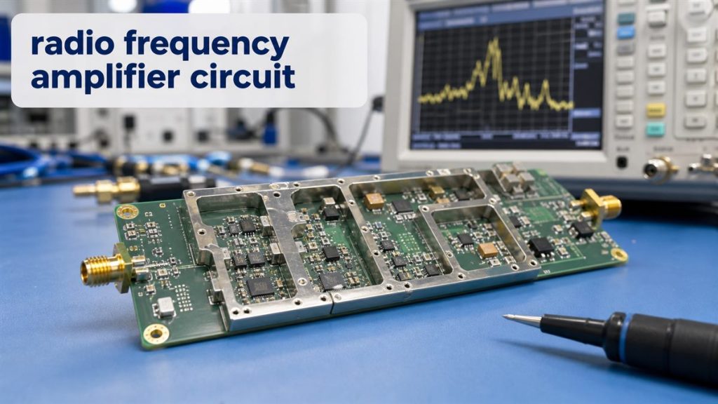
radio frequency amplifier circuit
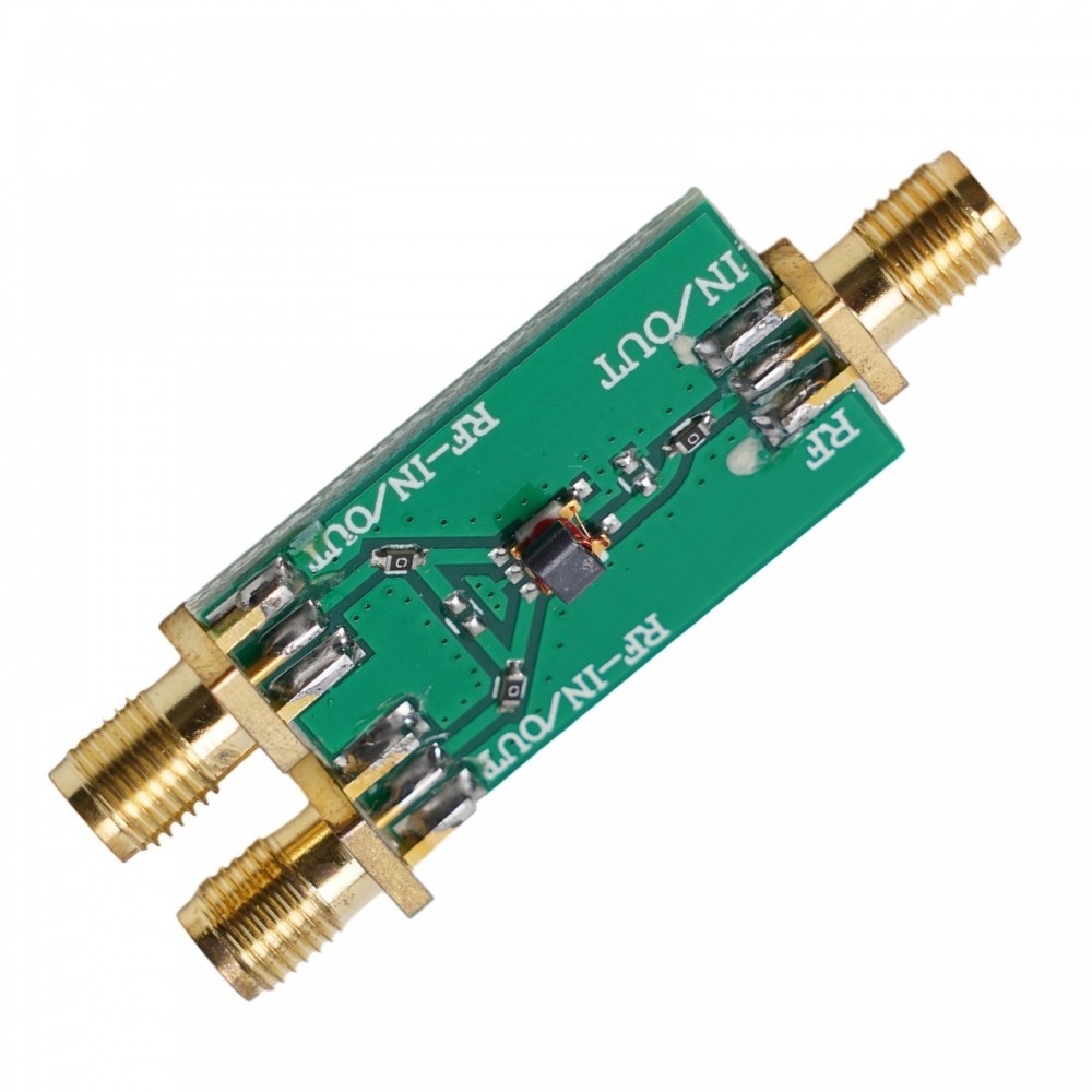
Radio frequency amplifier circuit PCB manufacturing review for RF materials, connectors, SMT, and testing.

What Is a Radio Frequency Amplifier Circuit?

A radio frequency amplifier circuit increases the strength of a high-frequency signal. It may be used near an antenna, inside a wireless module, in a signal repeater, or on a test board where RF signals need stable gain.

The PCB is not only a carrier for the circuit. At RF frequencies, the board becomes part of the signal path. Copper traces, dielectric material, ground return, vias, solder mask, pads, and connectors can all affect signal behavior.

Common applications include:

  • wireless communication modules
  • antenna front-end circuits
  • RF test boards
  • signal repeaters
  • IoT gateways
  • industrial RF sensors
  • high-frequency control boards
  • measurement equipment

For sourcing, the useful question is not only whether a supplier can make the PCB. The better question is whether the supplier can keep RF material, impedance, connector, SMT, and testing details visible before production starts.

Radio Frequency Amplifier Circuit Diagram and PCB File Review

A radio frequency amplifier circuit diagram helps explain the RF input, amplifier device, matching network, bias circuit, power filtering, ground reference, and RF output. But for production, the diagram is only one part of the project.

EBest Circuit needs the manufacturing files that define the real board:

FileWhy It Matters
Gerber / ODB++Copper, solder mask, outline, RF pads
StackupMaterial, dielectric thickness, copper thickness
BOMRF component value, package, sourcing
CPLPlacement position and orientation
Connector drawingFootprint, board edge, mounting method
Impedance notes50 ohm or other impedance control needs
Assembly drawingSoldering, shielding, cleaning, packing notes

EBest Circuit does not replace the customer’s RF design team. The amplifier topology, frequency band, gain target, noise figure, matching network, and RF performance decision should come from the customer’s engineering side. Our role is to check whether the PCB and PCBA files can be built reliably according to those requirements.

RF Amplifier Circuit Board Materials and Stackup

RF amplifier circuit board material selection depends on frequency, loss requirement, thermal need, cost, and product environment.

For some lower-frequency or cost-sensitive RF projects, FR4 may be acceptable. For higher-frequency or lower-loss RF applications, high-frequency laminate or hybrid material may be needed. EBest Circuit supports normal Tg FR4, mid Tg FR4, high TG PCB materials, Isola 370HR, FR408HR, Rogers 4003, Rogers 4350, Rogers 5880, Taconic material, PTFE material, and hybrid material options when required.

For RF boards, material choice affects dielectric constant, dielectric loss, impedance calculation, insertion loss, and stability. This is why stackup should be confirmed before fabrication, especially when the board includes SMA connectors, 50 ohm RF traces, shielding areas, or impedance reports.

A practical material review should answer:

  • What frequency range will the board support?
  • Is FR4 acceptable, or is a high-frequency material required?
  • Does the Dk/Df value affect the RF performance target?
  • Does the board need high Tg material for thermal reliability?
  • Is this a pure RF board or a hybrid RF + digital board?
  • Does the surface finish match solderability and RF requirements?

For RF boards above hundreds of MHz, material and process selection should be handled more carefully. For higher-frequency applications, dielectric loss, copper roughness, drilling, plating, and surface treatment become more sensitive.

50 Ohm Impedance in RF Amplifier PCB Manufacturing

Many RF amplifier PCB projects use 50 ohm single-ended impedance. The value is usually defined by the customer’s RF engineer, but the PCB manufacturer must build the physical structure consistently.

A 50 ohm trace is not decided by trace width alone. It depends on trace width, copper thickness, dielectric thickness, dielectric constant, reference ground layer, solder mask coverage, finished etching result, connector transition, and via/ground structure.

EBest Circuit’s PCB capability data shows that standard 1oz outer-layer line/space can reach 4/4mil in normal process and 3/3mil in special process. For RF amplifier PCB manufacturing, this matters because the finished trace is what the signal actually sees. If the design uses SMA connectors, the transition from connector pad to RF trace also needs attention. Ground pads, via fences, solder mask openings, and edge clearance should follow the customer-approved RF layout.

If an impedance report is required, the impedance coupon and testing requirement should be planned before production, not added after the board is finished.
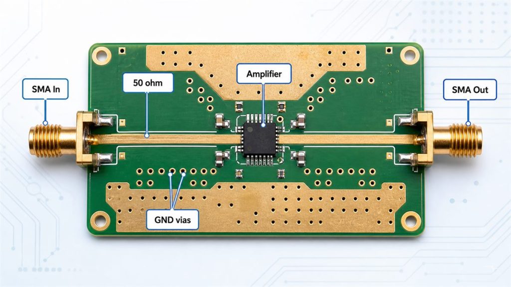
radio frequency amplifier circuit
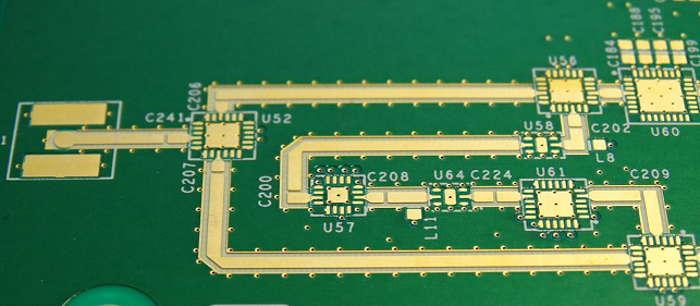
RF amplifier PCB routing depends on 50 ohm trace geometry, ground vias, connector transition, and stackup control.

Low Noise Amplifier Circuit PCB Manufacturing Checks

A low noise amplifier circuit is usually placed near the receiver side. The signal is weak, so the board should avoid adding unnecessary instability before the RF design can do its job.

For LNA boards, the manufacturing review is not about changing the RF design. It is about protecting the approved design during fabrication and assembly.

  • Do not change the RF input path without approval.
  • Keep the approved ground structure visible in production files.
  • Confirm RF component package and part number before sourcing.
  • Check small passive component footprints before SMT.
  • Review solder mask opening around RF pads.
  • Protect connector and RF input areas during handling.
  • Keep cleaning requirements clear when flux residue may matter.

A common risk is component substitution. In RF circuits, a capacitor, inductor, resistor, or filter may look like a standard component in the BOM, but its value, tolerance, package, ESR, Q factor, or approved manufacturer may matter. If sourcing changes are needed, they should be confirmed with the customer before SMT.

RF Power Amplifier Circuit Heat and Copper Requirements

An RF power amplifier circuit may generate more heat than a small-signal amplifier. The PCB must support both RF signal quality and thermal reliability.

EBest Circuit’s PCB capability data supports conventional FR4 inner copper from HOZ to 5oz and outer copper from 1oz to 5oz, with heavier copper available as a special process. This gives engineers more manufacturing options when an RF power board needs stronger current capacity or heat spreading.

Copper is not only about current. It can affect heat spreading, trace geometry, etching compensation, impedance calculation, solder mask bridge feasibility, board balance, warpage risk, and soldering quality.

If a power amplifier device has an exposed pad, large thermal pad, or heat-sensitive area, SMT process review is also important. Solder paste opening, void control, thermal vias, copper balance, and reflow profile can affect the final assembly.

For some high-power or heat-sensitive products, the project may also need metal core PCB, ceramic PCB, high-Tg FR4, or special thermal structure review. The right choice depends on power level, operating temperature, mechanical design, and customer test requirements.

SMT Assembly Risks for Radio Frequency Amplifier Circuit Boards

RF amplifier boards often include small passive components, RF filters, amplifier ICs, inductors, capacitors, shielding parts, SMA connectors, and sometimes QFN or BGA assembly requirements. The assembly risk is not only “can the component be placed?” The real question is whether the board can be soldered, inspected, cleaned, tested, and packed without damaging RF performance or connector reliability.

A practical SMT workflow may include:

incoming PCB and component review -> baking when required -> solder paste printing -> SPI -> placement -> reflow -> post-reflow inspection -> AOI -> X-Ray when BGA is involved -> hand soldering -> cleaning -> testing -> labeling -> depaneling -> packing

This process matters because many RF board problems appear before final testing. SPI can catch solder paste issues such as insufficient paste, offset, bridging risk, and paste height variation. SPI inspection accuracy around 10um is useful for fine components and RF matching areas.

  • RF passive value and package
  • connector orientation
  • solder paste volume near small components
  • soldering around SMA or RF terminals
  • flux residue near RF paths
  • shield can soldering
  • QFN/BGA inspection when used
  • packing protection for protruding connectors

Small quantity does not remove process risk. One failed prototype can delay debugging, RF validation, customer approval, and the next production build.

Testing and Inspection for RF Amplifier PCB Assembly

RF amplifier PCB assembly needs two different types of checks.

Manufacturing inspection: checks whether the board was made and assembled according to the production files.

RF performance testing: checks whether the circuit meets the customer’s electrical target.

For manufacturing-side control, EBest Circuit can support bare PCB electrical testing, impedance testing when required, AOI after SMT, X-Ray for BGA or hidden solder joints when needed, visual inspection of SMA connectors and RF terminals, solder joint and cleanliness inspection, and packing inspection before shipment.

For RF performance testing, the customer should define the test frequency, input signal condition, output condition, gain target, power level, load condition, acceptable tolerance, pass/fail criteria, and required test fixture or cable setup.

This distinction helps avoid confusion. A PCB supplier can verify manufacturing quality and coordinate customer-defined testing, but RF gain, noise figure, frequency response, and final electrical acceptance should be based on the customer’s approved test method.
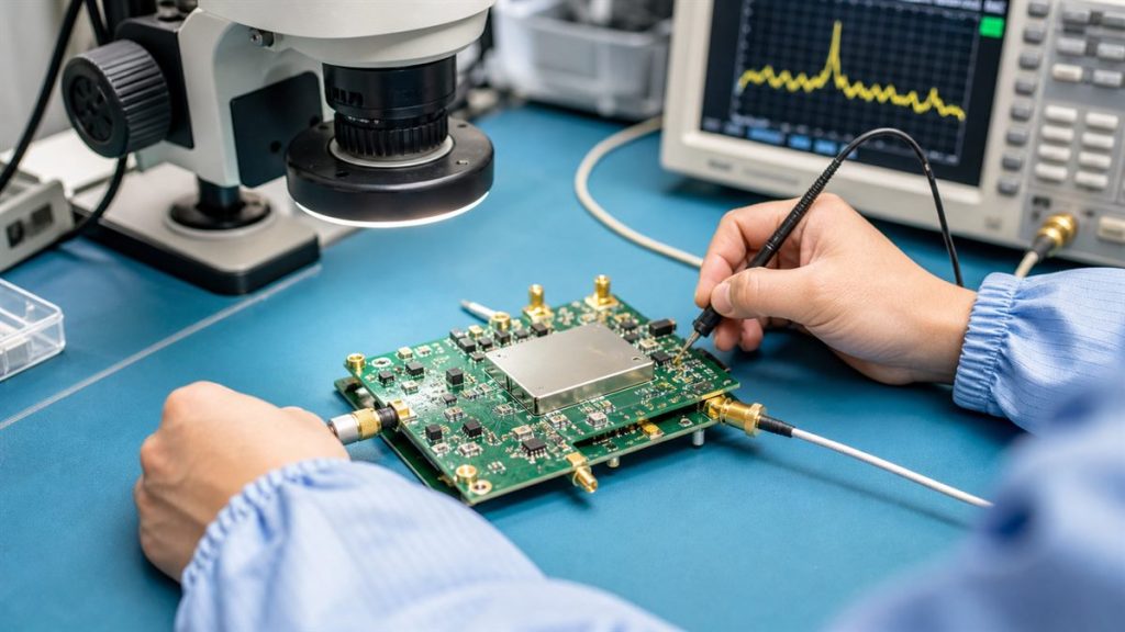
radio frequency amplifier circuit
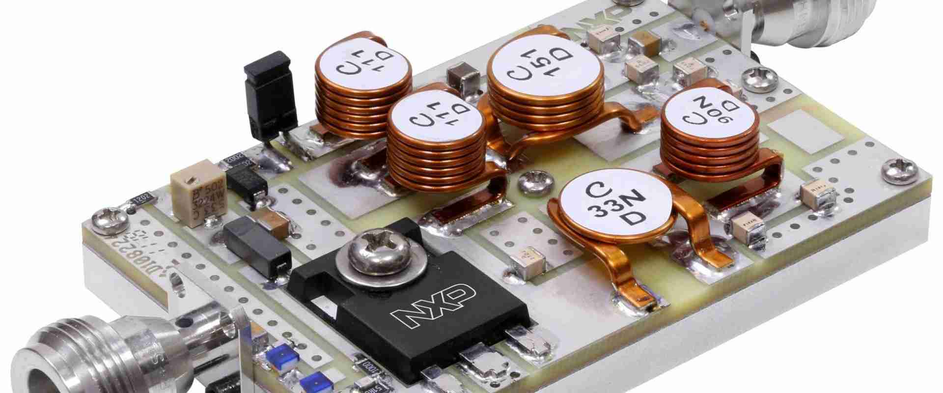
RF amplifier PCBA inspection should keep connector soldering, cleanliness, and customer-defined test conditions visible.

Radio Frequency Amplifier Circuit Manufacturing Case Study

A USA customer needed a small-batch RF amplifier PCB assembly for a wireless signal test module. The order quantity was not large, but the project had RF connector requirements, 50 ohm signal routing, small RF components, and assembly cleanliness requirements.

ItemRequirement
Customer regionUSA
ApplicationWireless RF signal test module
Quantity30 pcs prototype and pilot build
PCB type4-layer RF-related FR4 PCB
MaterialHigh-Tg FR4
Finished thickness1.6mm +/-10%
Copper1oz outer copper, 0.5oz inner copper
Surface finishENIG
RF requirement50 ohm signal path
AssemblySMT plus RF connector assembly
PackingSingle-unit protection after inspection

Main project risks:

  • The RF connector had to be soldered firmly and protected during packing.
  • The 50 ohm path had to match the customer-approved layout.
  • Small RF passives needed correct package, value, and approved sourcing.
  • RF areas needed clean soldering and inspection.
  • The first build had to support validation before the next production stage.

EBest Circuit solution:

  • Reviewed Gerber, stackup, BOM, CPL, connector drawing, and assembly notes together.
  • Checked RF trace area, connector footprint, ground vias, and solder mask opening.
  • Confirmed component packages and sourcing risks before SMT.
  • Used ENIG for stable solderability and surface protection.
  • Checked connector soldering, board cleanliness, and packing method before shipment.
  • Coordinated inspection and testing according to the customer’s project notes.

Result: The customer received a controlled RF amplifier PCBA pilot build for validation. The value was not only producing 30 boards. The value was keeping RF connector mounting, impedance-related PCB manufacturing, BOM preparation, SMT assembly, inspection, and packing requirements connected under one workflow.

FAQs About Radio Frequency Amplifier Circuit

1. What is a radio frequency amplifier circuit used for?

It is used to amplify RF signals in wireless communication, antenna systems, RF modules, signal repeaters, sensors, test equipment, and industrial electronics.

2. Does a radio frequency amplifier circuit always need a 50 ohm PCB trace?

Not always, but many RF amplifier PCB projects use 50 ohm impedance. The exact requirement should come from the customer’s RF design and product specification.

3. Can FR4 be used for an RF amplifier circuit board?

FR4 can be used for some lower-frequency or cost-sensitive RF projects. Higher-frequency, lower-loss, or more stable RF applications may require Rogers, PTFE, or other high-frequency materials.

4. What files should I send for RF amplifier PCB manufacturing?

Useful files include Gerber or ODB++, drill files, stackup, BOM, CPL, assembly drawing, impedance notes, connector drawing, and test requirements.

5. Can EBest Circuit design the RF amplifier circuit?

EBest Circuit supports PCB fabrication, DFM review, component sourcing, SMT assembly, inspection, and testing coordination. The RF circuit design, frequency target, gain requirement, and matching network should be confirmed by the customer’s RF engineering team.

All in all, a radio frequency amplifier circuit project should not be treated as only a schematic or only a bare PCB order. RF signal path, material, stackup, impedance, components, SMT assembly, connector reliability, inspection, and testing notes need to stay connected before production starts. If you are preparing an RF amplifier PCB or PCBA project, please send your Gerber files, stackup, BOM, connector drawing, impedance notes, and assembly requirements to sales@bestpcbs.com.
You may also like

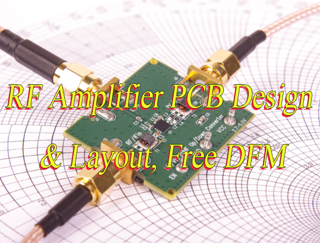
RF Amplifier PCB Design & Layout, Free DFM
Wednesday, December 3rd, 2025

How to design a RF amplifier PCB? This blog covers types, applications, technical parameter, design guideline and layout technique for RF amplifier PCB.

Are you troubled with these questions?

  • How to ensure PCB stability and low noise amid RF signal interference?
  • How to quickly optimize high-frequency impedance matching to avoid performance loss?
  • How to maintain stable high-frequency performance in mass production?

As a RF amplifier PCB manufacturer, EBest Circuit (Best Technology) can provide you service and solutions:

  • Precise Simulation & Optimization: Leverage ANSYS HFSS for EM simulation, cutting design iterations by 2-3 cycles with 40% efficiency gain. Achieve <5% signal integrity error and <0.8dB noise figure.
  • Impedance Matching Expertise: 20+ years of experience ensures ±3% impedance control via material selection and stack-up design, boosting matching efficiency by 20% and reducing signal loss by 15%.
  • Quality Control & Rapid Response: Full-process monitoring and S-parameter/eye-diagram testing ensure batch-to-batch high-frequency parameter deviation <±1%. Samples in 7 days, mass production in 15 days, with 98% on-time delivery rate.

Welcome to contact us if you have any request for RF amplifier PCB design and assembly: sales@bestpcbs.com.

What Is A RF Amplifier PCB?

A RF amplifier PCB is a circuit board created to support amplification stages that work in radio-frequency ranges. It carries components such as low-noise amplifiers, gain blocks, filters, bias circuits, and matching networks. Since RF energy reacts to small layout changes, the board must control impedance, grounding, and routing with more care than general PCBs. Furthermore, material choice, stack-up, and copper patterns influence how signals move through each trace. When these factors align, the amplifier remains stable, gains remain predictable, and unwanted radiation stays low.

What Is A RF Amplifier PCB

What Are Types of RF Amplifier PCBs?

  • Low-Noise Amplifier (LNA) PCB: These boards serve front-end systems in radios, satellite receivers, and radar sensors. Their goal is to lift micro-level input signals with very low added noise. LNAs rely on controlled impedance, a short input path, and a clean ground to reduce noise figure.
  • Power Amplifier (PA) PCB: PA boards push RF energy to a much higher level. They appear in transmitters, cellular base stations, industrial heating systems, and radar emitters. Because of higher current, these boards need thick copper, thermal relief paths, and stable bias networks.
  • Driver Amplifier PCB: A driver board takes medium-level signals and prepares them for a PA stage. It must handle some power while still keeping reasonable linearity.
What Are Types of RF Amplifier PCBs?

What Are Applications of RF Amplifier PCB Board?

  • 5G, LTE, and Wi-Fi systems in mobile devices and base stations.
  • Radar sensors used in autonomous driving, drones, and traffic monitoring.
  • Satellite communications for navigation, broadcasting, and remote sensing.
  • IoT nodes that need compact front-end amplification.
  • Test and measurement devices such as spectrum analyzers and signal generators.
  • Medical imaging and diagnostic tools that involve RF detection stages.
  • Industrial RF heating and plasma equipment.

RF Amplifier PCB Design Technical Parameter

ParameterTypical Specification
Operating Frequency Range0.5–6 GHz
Gain20±1 dB @ 25°C
Noise Figure (NF)≤1.2 dB (LNA) / N/A (PA)
Output Power (Pout)30 dBm (PA) / 10 dBm (Driver)
Output Third-Order Intercept Point (OIP3)+40 dBm
Voltage Standing Wave Ratio (VSWR)≤1.5:1 (Input/Output)
Operating Voltage+5V DC, ±10%
Operating Current120 mA (LNA) / 800 mA (PA)
Power Added Efficiency (PAE)>45% (PA)
PCB SubstrateRogers 4350B/Taconic RF-35/FR4-HF
Copper Thickness1–2 oz (35–70 μm)
Impedance Control Accuracy50Ω ±5%
Layer Count2–8 layers
Thermal Resistance (θja)≤15°C/W (PA with Heatsink)
Operating Temperature-40℃ ~ +85℃
Storage Temperature-55℃ ~ +125℃
Humidity Tolerance95% Non-condensing
EMC StandardsFCC Part 15, CE, RoHS 3
Lead-free ProcessCompliant (Sn96.5/Ag3.0/Cu0.5)
Mean Time Between Failures (MTBF)>100,000 hours
I/O InterfacesSMA/QMA/MMCX/Solder Pads
Shielding EnclosureOptional EMI Shielding Case
Test PointsIntegrated VNA Calibration Test Points

RF Amplifier PCB Design Guideline

A detailed guideline to RF amplifier PCB design:

1. Layout Partitioning and Isolation Design

  • Mixed-signal isolation: Strictly separate analog, digital, and RF zones. Maintain minimum spacing of 10mm (≥20mm for high-frequency applications) between digital circuits and RF sections to prevent cross-coupling. Implement “star” power routing to minimize noise crosstalk. Position sensitive components (e.g., LNAs, mixers) close to antennas or RF ports to reduce path length and losses.
  • Shielding and grounding: Use via fences (spacing ≤λ/20) to construct isolation bands. Install metal shielding enclosures (e.g., copper cavities) in sensitive areas. Ensure continuous ground planes without segmentation. Recommend dual-layer grounding with via stitching (spacing ≤λ/10) to enhance EMI protection.

2. Impedance Control and Transmission Line Design

  • Material selection: For frequencies above 1GHz, prioritize low-loss substrates (e.g., Rogers RO4350B, Taconic RF-35) over traditional FR4 (loss tangent 0.02-0.025). Materials must meet stable dielectric constant (Dk: 3.48±0.05@10GHz) and low moisture absorption (<0.1%).
  • Impedance matching: Transmission line characteristic impedance must precisely match standards (e.g., 50Ω). Use microstrip/stripline structures and avoid 90° bends; adopt 45° miters or curved transitions. Validate stackup designs with field solvers (e.g., Polar Si8000) to maintain <±10% impedance tolerance.

3. Power and Thermal Management

  • Decoupling and filtering: Deploy multi-stage filtering (LC/π networks) at power entry points. Place small-value (0.1μF) ceramic capacitors near ICs combined with bulk (10μF) electrolytic capacitors in “star” topology to reduce IR drops.
  • Thermal design: Under high-power devices (e.g., PAs), implement thermal via arrays filled with conductive adhesive. Integrate heat sinks or metal-core substrates (e.g., aluminum) to enhance heat dissipation, ensuring junction temperature remains below 125°C.

4. Signal Integrity and EMC Protection

  • Routing rules: Avoid cross-layer via transitions for RF signal lines. When necessary, use via-in-pad or back-drilling to eliminate stubs. Maintain ≥3× line width spacing between high-speed digital signals and RF traces, or employ differential pairs for balanced transmission.
  • EMI suppression: Install ground traces along board edges and common-mode chokes at critical interfaces. Optimize layouts through simulation (ADS/HFSS) and ensure compliance with FCC/CE radiation limits (e.g., EN55022).

5. Manufacturing and Testability Design

  • Process specifications: Adhere to IPC-6012 standards. Define minimum trace width/spacing compatible with manufacturing capabilities (e.g., 100μm for HDI processes). Specify stackup details including layer thickness, copper weight, and solder mask dimensions.
  • Test validation: Include test points (e.g., SMA connectors) and debugging pads. Deploy temperature rise monitoring at critical nodes. Verify S-parameters (e.g., S21, S11) with network analyzers to confirm gain and noise figure specifications.

6. Documentation and Regulatory Compliance

  • Design documentation: Provide complete BOM, Gerber files, stackup reports, and simulation models. Annotate critical parameters (Dk/Df values, thermal resistance curves) with international certifications (UL, RoHS).
  • Regulatory adaptation: Configure power filtering solutions to meet regional standards (e.g., IEC 61000-4-2 ESD requirements for EU/NA markets).
RF Amplifier PCB Design Guideline

RF Amplifier PCB Layout Technique

Below are some techniques of RF amplifier PCB layout for your reference:

Signal Flow and Layout Planning

    • Linear Layout Principle: Arrange the main signal path in a “linear” configuration within the shielding cavity, avoiding U-shaped or complex paths to minimize self-interference. Use L-shaped layouts when space is constrained. Multi-channel systems require fully symmetric layouts to ensure phase consistency.
    • Functional Partition Isolation: Isolate digital, analog, and RF circuits physically. High-Power Amplifiers (HPA) and Low-Noise Amplifiers (LNA) must be separated by ≥5mm or placed on different layers. Use cavity isolation for sensitive circuits and strong radiation sources, and add shielding between multi-stage amplifier stages.

    Ground System Design

      • Grounding Method Selection: Single-point grounding for low-frequency control signals; multi-point grounding (via spacing ≤λ/20) for high-frequency RF signals. Partition ground layers by function (RF, digital, power) and connect them at a single point.
      • Ground Via Arrays: Place ground vias on both sides of RF microstrip lines (spacing 0.5-1mm) to form an electromagnetic barrier. Ensure shielding cavity bottom grounding impedance ≤0.1Ω to avoid secondary radiation.

      Power Decoupling and Filtering

        • Star Power Routing: Use a star configuration for power networks. Parallel large capacitors (e.g., 10μF electrolytic) and small capacitors (0.1μF MLCC) at the root node to extend the frequency band. Place capacitors close to power pins and connect ground terminals via short leads to the ground plane.
        • Pi-Type Filter: Add a pi-type filter (series RFC with impedance ≥1kΩ@operating frequency + parallel capacitor) at the power input to suppress high-frequency noise. Example: Adding a pi-type filter to a 10W PA power terminal reduces ripple from 200mV to 10mV.

        Signal Routing and Impedance Control

          • 50Ω Impedance Design: RF signal line width ≥15mil. Use cross-layer references to ensure stable impedance. Use rounded corners instead of right angles. Maintain a 2W spacing (minimum 1W) between RF traces and ground copper.
          • Sensitive Signal Isolation: Keep analog small signals away from high-speed digital and RF signals. Maintain a clearance of ≥5mm in all layers for antenna areas to reduce interference.

          Thermal Management and Heat Dissipation

            • Heat Dissipation Solutions: Use copper/aluminum heat sinks for high-power amplifiers, combined with natural convection or forced air cooling. Use liquid cooling/heat pipes in extreme cases. Fill the gap between the chip and the heat sink with thermal grease or phase-change material to reduce thermal resistance.
            • Thermal Vias and Copper Layers: Add thermal vias, thicken copper layers, optimize the layout of high-heat components, and avoid clustering heat-sensitive areas. Integrate temperature sensors to trigger over-temperature protection.

            Electromagnetic Compatibility and Shielding

              • Metal Shielding Cavity: Enclose high-power amplifiers in aluminum/brass shielding cavities (thickness 0.2-0.5mm) with grounding impedance ≤0.1Ω. Add ventilation holes (diameter ≤λ/20) or attach heat sinks to the top.
              • Filtering Techniques: Use pi-type or LC filters on power and signal lines to suppress conducted and radiated interference. Add series resistors/magnetic beads to control signal lines and attenuators to RF test points.
              RF Amplifier PCB Layout Technique

              Why Partner With EBest Circuit (Best Technology) for RF Amplifier PCB Manufacturer?

              Reasons why choose EBest Circuit (Best Technology) for RF amplifier PCB manufacturer:

              • Global Certification Standards Compliance: Certifications include ISO 9001 quality management, IATF 16949 automotive standards, medical-grade ISO 13485, and RoHS environmental compliance. These certifications meet high-standard requirements across consumer electronics, automotive, medical, and global market access conditions.
              • 19 Years of Industry Expertise: With 19 years of specialized experience in RF PCB manufacturing and over 5,000 successful projects, expertise includes high-frequency substrate processing, microstrip impedance control, and thermal optimization. This experience enables rapid identification and resolution of design-related manufacturing risks.
              • Free DFM Manufacturability Analysis: Senior engineering teams provide free DFM analysis to proactively identify manufacturability issues such as overly small trace widths, spacing, or pad design flaws. This reduces redesign costs, shortens time-to-market, and improves mass production yield.
              • Competitive Pricing with Cost-Sensitive Design Solutions: Leverage economies of scale and process optimization to deliver market-leading quotes. Customize cost-sensitive solutions tailored to client designs, such as alternative high-performance materials or streamlined production flows, directly reducing manufacturing costs by 30%-50% for budget-sensitive RF amplifier projects.
              • 24-Hour Rapid Prototyping for Urgent Orders: Dedicated rapid-response teams enable 24-hour turnaround from order placement to sample delivery. Parallel engineering processes and pre-stocked material libraries ensure R&D timelines remain unaffected, helping clients seize market opportunities ahead of competitors.
              • 99.2% On-Time Delivery Rate: Intelligent production scheduling systems and real-time supply chain monitoring achieve end-to-end process visibility. Historical data confirms a 99.2% on-time delivery rate, significantly exceeding industry averages and ensuring stable client production planning.
              • Batch Production Full Inspection and Rigorous Quality Control: Each production batch undergoes 100% inspection via AOI optical testing, X-ray layer inspection, and electrical performance verification. Combined with SPC statistical process control, key RF parameters like gain and noise figure maintain consistency, with defect rates controlled below 0.08%.
              • Flexible Production Scalability: Automated production lines support full lifecycle services from prototyping to mass production. Capability to rapidly adjust capacity accommodates small-batch trial production to high-volume orders, avoiding overcapacity risks while ensuring seamless transitions between production scales.

              Feel free to contact us at sales@bestpcbs.com if you have any inquiry for RF amplifier PCB design, production and assembly.

              Common FAQs to Avoid in RF Amplifier PCB Design

              Q1: Why does a poor ground system cause instability in an RF amplifier PCB?

              A1: weak ground system raises return-path impedance and increases the chance of unintended coupling. When the RF return path does not flow under its matching trace, the loop grows larger and the amplifier becomes sensitive to noise and oscillation. Using a solid ground plane and many stitching vias shortens the loop and keeps the board stable at high frequency.

              Q2: What happens if RF traces are longer than necessary?

              A2: Long traces add loss, increase parasitic inductance, and create phase shifts that distort gain. They also pick up more noise from nearby circuits. RF input traces should be as short and direct as possible. Shorter routing keeps the amplifier’s noise figure low and preserves signal strength.

              Q3. Why is placing matching networks far from the device a common mistake?

              A3: Matching networks work only when placed close to amplifier pins. If they sit too far away, the trace between the device and matching parts becomes part of the matching network itself. This shifts impedance, raises reflection, and weakens overall gain. Keeping these components close maintains predictable matching.

              Q4: What risk appears when digital and RF circuits are not isolated?

              A4: Digital circuits generate sharp edges that spread electromagnetic noise. When digital zones sit near RF paths, this noise couples into the amplifier stage, causing ripple, distortion, and reduced sensitivity. Placing digital, RF, and power areas separately lowers interference and supports smoother performance.

              Q5: Why does ignoring thermal relief cause failures in power RF amplifiers?

              A5: Power amplifiers release heat during normal operation. If the board lacks enough copper area, thermal vias, or heat-spreading design, temperature rises quickly and shifts gain, bias, or linearity. In severe cases, the device may degrade. Good thermal planning keeps temperature stable and extends the amplifier’s usable life.

              You may also like