PCB manufacturing PCB manufacturing
Home > Blog

High-Frequency PCB Materials

June 4th, 2026

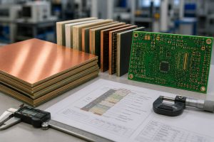
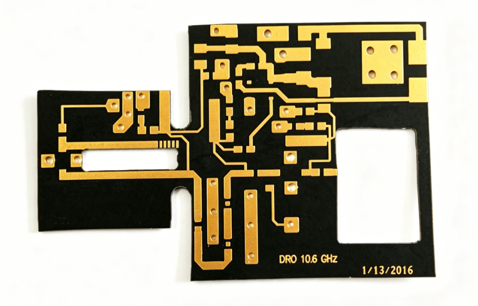
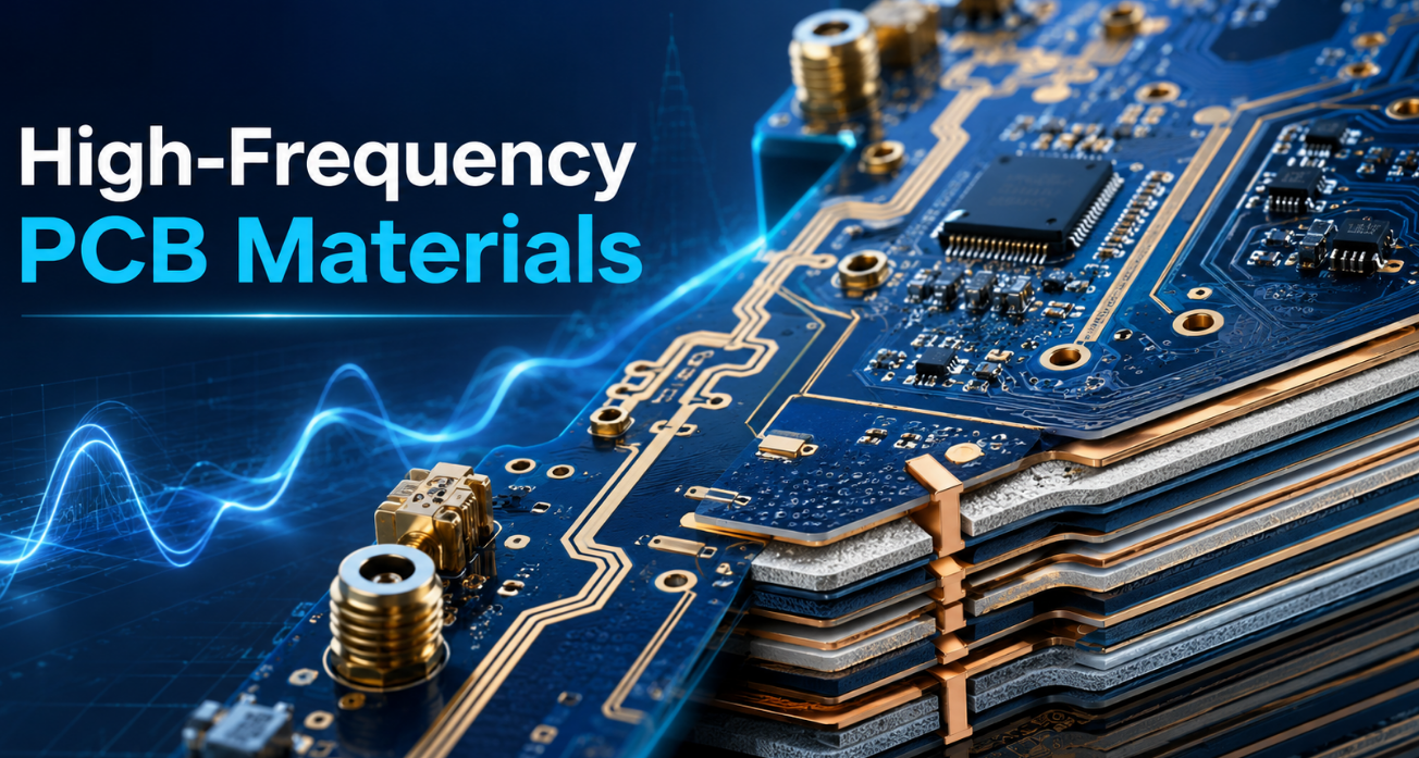
High-frequency PCB materials are used when a circuit board must support stable signal transmission, low dielectric loss, controlled impedance, and reliable RF performance. In RF, microwave, radar, antenna, 5G, satellite, and high-speed communication products, standard FR4 may not provide enough electrical stability at higher frequencies. This is why many projects use Rogers PCB materials, low-loss laminates, PTFE-based materials, ceramic-filled materials, or hybrid high-frequency stack-ups.

The right material choice affects insertion loss, return loss, phase stability, impedance accuracy, thermal behavior, moisture resistance, manufacturability, and final product reliability. For procurement and engineering teams, high-frequency PCB material selection is not only about choosing a famous material brand. It requires a full review of frequency, Dk, Df, copper roughness, board thickness, stack-up, surface finish, testing method, and production capability.
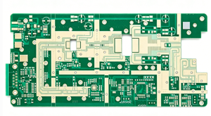
high-frequency PCB materials, https://www.bestpcbs.com/blog/2026/06/high-frequency-pcb-materials/

What Are High-Frequency PCB Materials?

High-frequency PCB materials are special circuit board laminates designed for RF, microwave, millimeter-wave, and high-speed signal applications. Compared with standard FR4, they provide lower signal loss, more stable dielectric properties, better impedance control, and stronger frequency performance.

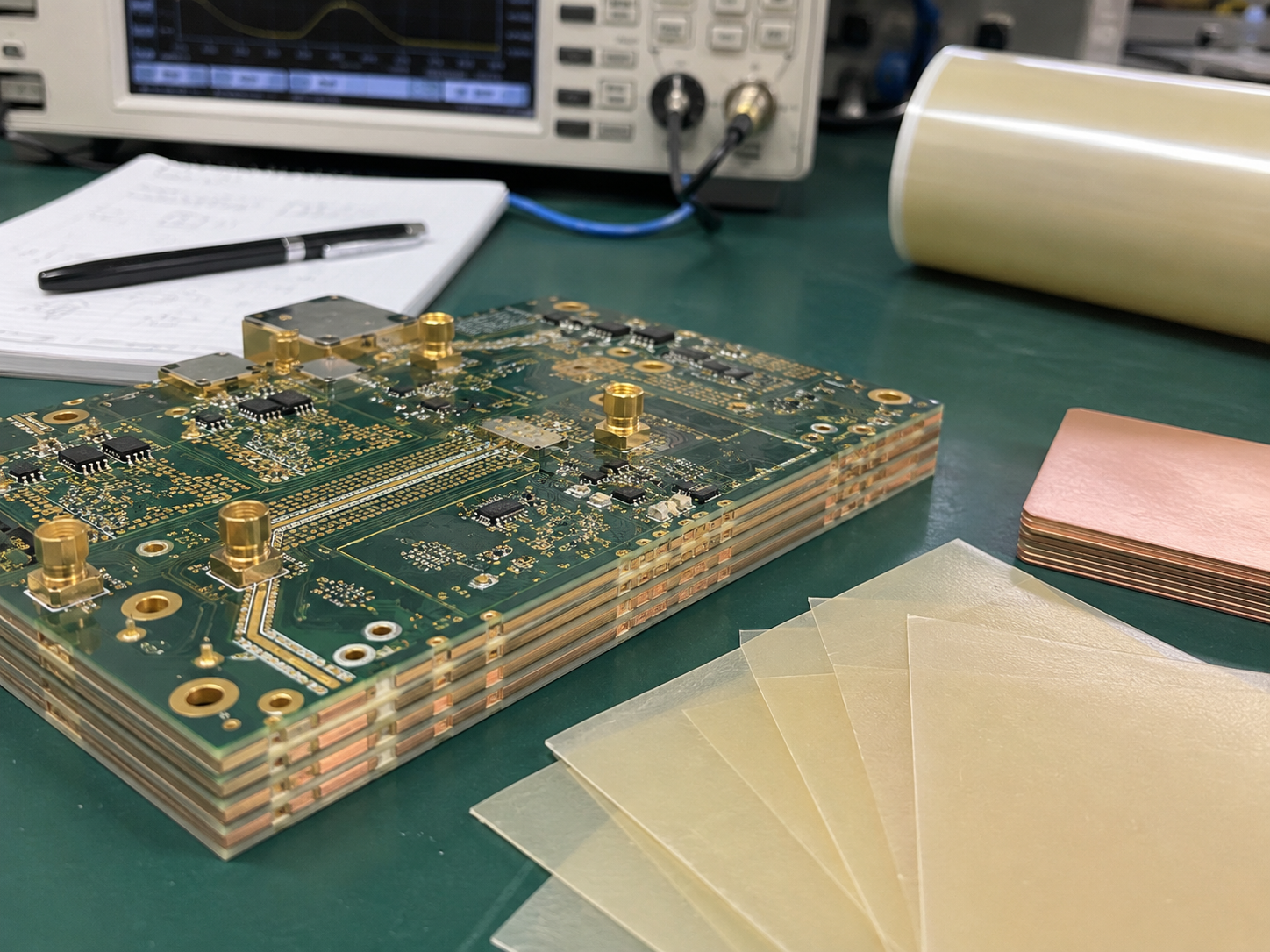
Common high-frequency PCB materials include Rogers PCB materials, PTFE-based laminates, hydrocarbon ceramic laminates, low-loss FR4 alternatives, ceramic-filled materials, and hybrid RF laminates. Rogers PCB materials are widely used because they offer several laminate families for RF, microwave, antenna, radar, 5G, and high-speed applications.

These materials are selected when the PCB must behave as part of the signal path, not only as a mechanical support. In high-frequency circuits, small material changes can affect signal speed, wavelength, resonance, phase delay, impedance, and RF testing results.

Why Are High-Frequency PCB Materials Important?

High-frequency PCB materials are important because signal behavior becomes more sensitive as frequency increases. At higher frequencies, dielectric loss, conductor loss, copper roughness, dielectric thickness variation, and impedance mismatch can all reduce circuit performance.

If the wrong material is selected, the PCB may suffer from high insertion loss, unstable antenna tuning, poor return loss, phase drift, EMI issues, weak RF output, or inconsistent batch performance. These problems may not appear in a simple open-short electrical test, but they can fail during RF testing or real product operation.

For applications such as 5G antennas, radar modules, RF power amplifiers, microwave filters, satellite boards, and high-speed test equipment, high-frequency PCB materials directly affect product reliability, signal quality, and production yield.

How Do High-Frequency PCB Materials Work?

High-frequency PCB materials work by providing a stable dielectric environment for electromagnetic signal transmission. The dielectric layer controls signal propagation, while the copper foil, trace geometry, reference plane, and laminate thickness control impedance and signal loss.

Key material properties include dielectric constant, dissipation factor, dielectric thickness, copper roughness, moisture absorption, thermal conductivity, coefficient of thermal expansion, and dimensional stability. These properties must remain stable across frequency, temperature, humidity, and production batches.

For example, a small shift in dielectric constant may change impedance or antenna resonance. A rough copper surface may increase conductor loss at microwave frequencies. A weak lamination process may create reliability problems in hybrid stack-ups. That is why high-frequency PCB material selection must be connected with both RF design and PCB manufacturing control.

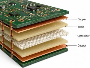
What Is the Structure of a High-Frequency PCB?

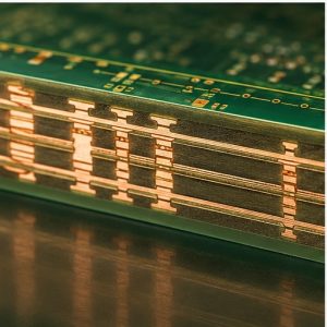
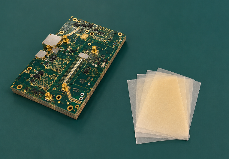
A high-frequency PCB usually includes high-frequency laminate, copper foil, bonding material, ground plane, solder mask, surface finish, and sometimes FR4 supporting layers. The exact structure depends on the frequency range, impedance requirement, layer count, thermal load, and assembly method.

Layer / MaterialMain FunctionKey Selection Points
High-frequency laminateProvides RF dielectric baseDk, Df, thickness, stability
Copper foilCarries RF signals and currentRoughness, thickness, peel strength
Bondply or prepregBonds multilayer structuresDk match, flow control, lamination reliability
Ground planeControls return path and shieldingCopper thickness, spacing, flatness
Solder maskProtects copper areasRF impact, adhesion, heat resistance
Surface finishSupports soldering and contact qualityENIG, immersion silver, OSP, hard gold

For RF boards, dielectric thickness and copper roughness are especially important. Even small changes in these areas can shift impedance, increase insertion loss, or change resonance behavior.

What Types of High-Frequency PCB Materials Are Common?

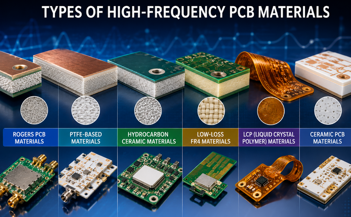
High-frequency PCB materials can be grouped by resin system, electrical performance, cost level, and application area. Common types include Rogers PCB materials, PTFE laminates, hydrocarbon ceramic laminates, low-loss FR4 materials, LCP materials, and ceramic PCB materials.

Material TypeTypical FeaturesCommon Applications
Rogers PCB materialsStable RF performance, multiple laminate familiesRF modules, radar, antennas, 5G
PTFE laminatesVery low loss, strong microwave performanceMicrowave, satellite, defense
Hydrocarbon ceramic laminatesGood RF performance and manufacturabilityCommercial RF, antennas, filters
Low-loss FR4Lower cost than advanced RF laminatesHigh-speed digital, moderate frequency
LCP materialsLow moisture absorption, good RF performanceAntenna, flexible RF, compact modules
Ceramic PCB materialsHigh thermal stability and insulationRF power, laser, aerospace, medical

The best choice depends on frequency, loss budget, board size, cost target, thermal demand, manufacturing process, and test requirements. Rogers PCB materials are often selected when projects need a practical balance of RF performance and manufacturability.
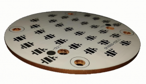
high-frequency PCB materials types, https://www.bestpcbs.com/blog/2026/06/high-frequency-pcb-materials/

What Are Rogers PCB Materials?

Rogers PCB materials are advanced circuit laminates used for high-frequency, RF, microwave, and high-speed electronic products. They are known for low dielectric loss, stable dielectric constant, controlled thickness, and reliable RF performance.

Common Rogers material families include RO4000 Series, RO3000 Series, RT/duroid materials, TC Series materials, and other high-speed circuit materials. These materials are used in antennas, RF front-end modules, radar boards, satellite communication systems, microwave circuits, and 5G infrastructure.

Rogers PCB materials are not selected only because of the brand name. They are chosen because specific Rogers laminates can provide predictable Dk, low Df, stable impedance behavior, and better RF repeatability compared with standard FR4 materials.

What Are RO4000 Series Materials?

RO4000 Series materials are commonly used in commercial RF and microwave PCB projects. They are often selected when the design needs better RF performance than FR4, but still requires practical processing, reasonable cost, and stable production.

RO4003C, RO4350B, and related Rogers PCB materials are widely used in RF modules, antennas, microwave boards, filters, power amplifiers, and communication systems. They offer a useful balance between electrical performance and manufacturability.

For many RF projects, RO4000 materials are a practical choice because they can support controlled impedance, low loss, stable fabrication, and cost control better than many high-end PTFE-only options.

What Are RO3000 Series Materials?

RO3000 Series materials are ceramic-filled PTFE composites used for more demanding microwave and RF applications. They are often selected when the circuit requires stable dielectric constant, low loss, and good dimensional control.

RO3003, RO3006, RO3010, and related Rogers PCB materials are commonly used in radar systems, microwave circuits, antenna products, multilayer RF designs, 5G modules, and high-frequency test equipment.

These materials are especially useful when a project needs stable electrical behavior across frequency and temperature. For radar and microwave products, this stability can help reduce frequency drift, phase error, and inconsistent RF test results.

What Are RT/duroid Materials?

RT/duroid materials are high-performance Rogers PCB materials used in demanding RF, microwave, aerospace, defense, satellite, and broadband applications. They are often selected when the design requires very low loss, stable signal behavior, and high reliability.

These materials are common in satellite communication boards, radar systems, phased-array antennas, microwave modules, aerospace electronics, and defense-grade RF circuits. They can provide excellent high-frequency performance, but usually require stricter fabrication control.

Compared with more cost-balanced high-frequency PCB materials, RT/duroid laminates may increase material and processing cost. However, they are often justified when the project has strict RF loss, phase stability, or reliability requirements.

What Material Properties Matter Most?

The most important properties of high-frequency PCB materials include Dk, Df, copper roughness, dielectric thickness, thermal conductivity, CTE, moisture absorption, and dimensional stability.

PropertyWhy It Matters
Dielectric constantControls impedance, wavelength, antenna size, and phase
Dissipation factorAffects dielectric loss and signal efficiency
Copper roughnessIncreases conductor loss at higher frequencies
Thickness toleranceAffects impedance and coupling accuracy
Thermal conductivityHelps control RF power heat rise
Moisture absorptionReduces frequency drift in humid environments
CTEAffects plated hole and lamination reliability
Dimensional stabilitySupports registration and repeatable production

A low Df value is important, but it is not the only selection factor. A material can still create problems if thickness tolerance, copper profile, lamination behavior, or fabrication capability is not suitable for the design.

How Do High-Frequency PCB Materials Compare with FR4?

High-frequency PCB materials and FR4 are used for different performance levels. FR4 is suitable for general electronics, control boards, and many digital circuits. High-frequency PCB materials are used when signal loss and dielectric stability become critical.

Comparison ItemHigh-Frequency PCB MaterialsStandard FR4
Signal lossLower loss at RF and microwave frequenciesHigher loss at high frequencies
Dk stabilityMore controlled and stableLess stable at high frequency
Impedance controlBetter for RF and microwave circuitsSuitable for general circuits
CostHigherLower
Manufacturing difficultyRequires tighter process controlEasier and widely available
Best useRF, radar, antenna, microwave, 5GControl boards, standard electronics
Main riskHigher cost and process sensitivityLimited RF performance

FR4 can still work in some lower-frequency or cost-sensitive designs. However, for antennas, RF filters, radar boards, microwave modules, and high-speed communication products, high-frequency PCB materials are usually more reliable.
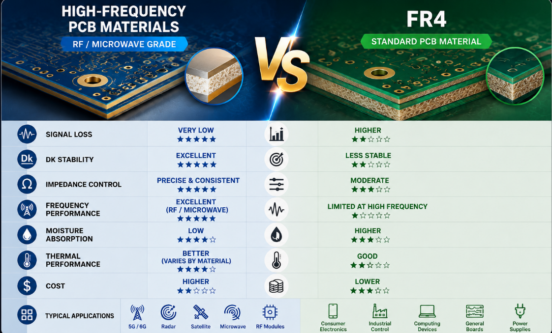
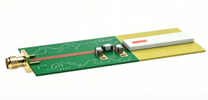
High-Frequency PCB Materials vs FR4, https://www.bestpcbs.com/blog/2026/06/high-frequency-pcb-materials/

How Do Rogers PCB Materials Compare with Other High-Frequency PCB Materials?

Rogers PCB materials are one category of high-frequency PCB materials. They are often compared with PTFE laminates, low-loss FR4, LCP, and ceramic PCB materials.

Comparison ItemRogers PCB MaterialsLow-Loss FR4Ceramic PCB Materials
RF performanceStrong and stableModerateStrong in RF and thermal applications
CostMedium to highLowerUsually higher
FabricationDepends on material familyEasierSpecialized process
Thermal behaviorVaries by seriesModerateOften excellent
Mechanical behaviorLaminate-based PCB processSimilar to FR4Hard but brittle
Best useRF, microwave, radar, antenna, 5GHigh-speed digital, lower RF demandRF power, laser, medical, aerospace

Rogers PCB materials are often preferred when the project requires better RF stability than low-loss FR4, but still needs practical PCB fabrication. Ceramic materials may be selected when thermal conductivity, insulation stability, or high-power operation becomes more important.

What Manufacturing Challenges Occur with High-Frequency PCB Materials?

High-frequency PCB materials require tighter manufacturing control than standard FR4. Common challenges include drilling quality, plating reliability, copper adhesion, lamination control, registration accuracy, surface cleanliness, impedance variation, and material handling damage.

PTFE-based materials may require special drilling, plasma treatment, or surface preparation. Hybrid stack-ups using Rogers PCB materials and FR4 also require careful control of CTE mismatch, lamination cycle, material flow, and layer registration.

Small manufacturing variations can create large RF differences. Rough copper, dielectric thickness variation, poor etching, weak plating, or contamination can increase loss and shift impedance.

What Design Rules Matter for High-Frequency PCB Materials?

Design rules for high-frequency PCB materials should focus on electrical behavior, not only routing space. Important rules include controlled impedance, short RF paths, smooth trace transitions, stable ground reference, proper via placement, and clear stack-up definition.

For antenna and microwave circuits, avoid unnecessary stubs, sharp corners, uncontrolled dielectric changes, and inconsistent ground spacing. Trace width, dielectric thickness, copper roughness, and surface finish should be reviewed together.

For hybrid designs, clearly define which layers use Rogers PCB materials and which layers use FR4 or other materials. This helps reduce quotation errors, production confusion, and RF test failure risk.

What Surface Finishes Are Used for High-Frequency PCBs?

Common surface finishes for high-frequency PCBs include ENIG, immersion silver, OSP, immersion tin, and hard gold. The right finish depends on solderability, contact requirements, shelf life, cost, and RF sensitivity.

Surface FinishAdvantagesCommon Use
ENIGFlat surface and good shelf lifeRF modules, fine-pitch assembly
Immersion silverGood conductivity and solderabilityRF and microwave circuits
OSPThin and cost-effectiveFast assembly projects
Immersion tinGood flatnessSelected soldering applications
Hard goldWear resistanceRF contacts, edge connectors

Surface finish can affect RF performance at microwave and millimeter-wave frequencies. For sensitive circuits, finish thickness, surface roughness, and pad geometry should be reviewed before production.

What Quality Tests Are Needed for High-Frequency PCB Materials?

High-frequency PCB materials require both standard PCB inspection and RF-related verification. Quality tests may include electrical test, impedance test, AOI, X-ray, dimensional inspection, cross-section analysis, solderability testing, thermal stress testing, and RF testing when required.

Test ItemPurpose
Electrical testChecks open and short circuits
Impedance testConfirms controlled impedance performance
AOIDetects trace defects and spacing issues
X-ray inspectionChecks hidden structures and vias
Cross-sectionChecks plating, hole wall, and lamination quality
Dimensional inspectionVerifies outline, holes, and registration
Solderability testConfirms assembly readiness
RF testConfirms insertion loss, return loss, or antenna performance

A board may pass standard electrical testing but still fail RF performance. For high-frequency projects, impedance control and RF testing are often more meaningful than open-short testing alone.

What Common Problems Happen with High-Frequency PCBs?

Common problems include impedance mismatch, high insertion loss, poor return loss, delamination, drilling defects, plating failure, registration shift, soldering issues, contamination, and unstable RF test results.

Impedance mismatch may come from wrong material data, dielectric thickness variation, inaccurate etching, incorrect copper thickness, or poor stack-up control. High insertion loss may result from high Df material, rough copper, long trace paths, or unsuitable surface finish.

Many failures are caused by incomplete communication before production. The manufacturer should know exact material grade, copper thickness, dielectric thickness, impedance target, surface finish, stack-up, and RF test requirements before manufacturing starts.

How to Choose the Right High-Frequency PCB Materials?

Choosing the right high-frequency PCB materials starts with frequency, signal type, loss budget, power level, impedance target, board size, operating temperature, and product environment.

For cost-sensitive RF designs, RO4000 Series Rogers PCB materials may be practical. For more stable microwave multilayer designs, RO3000 Series materials may be considered. For low-loss aerospace, satellite, broadband, or defense applications, RT/duroid materials may be suitable.

A good selection process should review Dk, Df, thickness tolerance, copper roughness, thermal performance, surface finish, fabrication complexity, material availability, and test requirements together. The best material is the one that meets RF performance and production reliability at the same time.

What Factors Affect the Cost of High-Frequency PCB Materials?

High-frequency PCB cost depends on material grade, laminate thickness, copper thickness, layer count, impedance tolerance, via structure, surface finish, drilling difficulty, testing requirements, and order quantity.

Cost FactorWhy It Affects PriceCost Control Suggestion
Material gradeRogers PCB materials and specialty laminates cost moreMatch material to real RF demand
Layer countMore layers increase lamination complexityKeep RF stack-up as simple as possible
Impedance toleranceTight tolerance requires more process controlUse realistic tolerance where possible
Copper profileLow-profile copper may cost moreUse where insertion loss matters
Surface finishENIG, silver, or hard gold affects costChoose based on RF and assembly needs
RF testingSpecial testing adds time and costDefine required test items early
QuantitySmall batches have higher setup costPlan prototype and batch needs together

Choosing a cheaper material may not reduce total cost if the board fails RF testing. Material selection should balance performance, manufacturability, and long-term reliability.

Where Are High-Frequency PCB Materials Commonly Used?

High-frequency PCB materials are used in products that require stable RF, microwave, millimeter-wave, or high-speed signal performance.

5G and wireless communication: antennas, RF front-end boards, base station modules, filters, and power amplifiers.

Automotive electronics: radar modules, ADAS sensors, vehicle communication systems, and high-frequency control units.

Aerospace and defense: radar systems, satellite communication boards, avionics, phased-array systems, and microwave modules.

Industrial electronics: RF sensors, test instruments, measurement equipment, and high-speed control modules.

Medical electronics: RF imaging systems, high-frequency diagnostic equipment, and compact signal modules.

Consumer and IoT products: wireless modules, high-frequency antennas, wearable communication products, and smart devices.

What Should You Confirm Before Ordering High-Frequency PCBs?

Before ordering high-frequency PCBs, confirm material grade, laminate thickness, copper thickness, stack-up, impedance target, surface finish, tolerance, via structure, solder mask requirement, and testing method.

You should provide Gerber files, drill files, stack-up drawings, impedance requirements, RF performance notes, material callouts, quantity, and assembly requirements. If the board uses Rogers PCB materials in a hybrid stack-up, clearly mark which layers use Rogers and which layers use FR4.

For RF projects, prototype validation is strongly recommended before mass production. Testing real boards under working frequency conditions helps confirm whether the selected material, stack-up, and fabrication process match the design goal.

Why Choose EBest for High-Frequency PCB Manufacturing?

EBest Technology provides one-stop PCB solutions, including PCB design, PCB prototype, mass production, component sourcing, PCB assembly, and box-build assembly. Its product range includes standard FR4 PCB, metal-based PCB, ceramic PCB, flexible PCB, rigid-flex PCB, and high frequency PCB, supporting different electronic manufacturing needs.

For high-frequency PCB projects, EBest can support material review, Rogers PCB materials selection, stack-up confirmation, controlled impedance production, prototype validation, batch manufacturing, PCB assembly, and quality inspection. This is useful for RF modules, antennas, communication boards, radar boards, microwave products, and high-speed electronic systems.

EBest also supports quality and compliance systems such as IATF 16949, ISO 9001:2015, ISO 13485:2016, AS9100D, REACH, RoHS, and UL-related requirements. These capabilities help customers manage industrial, automotive, medical, aerospace, and export-oriented high-frequency PCB projects with more confidence.
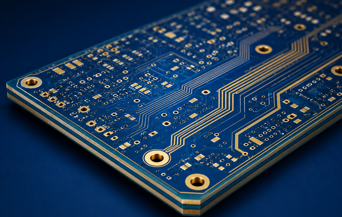
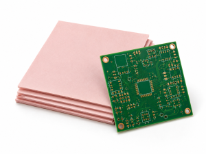
high frequency PCB, https://www.bestpcbs.com/blog/2026/06/high-frequency-pcb-materials/

FAQs About High-Frequency PCB Materials

Q1: What are high-frequency PCB materials used for?
A1: High-frequency PCB materials are used for RF, microwave, radar, antenna, 5G, satellite, aerospace, and high-speed communication circuits. They help reduce signal loss, control impedance, improve frequency stability, and support more predictable electrical performance than standard FR4.

Q2: Are Rogers PCB materials the same as high-frequency PCB materials?
A2: Rogers PCB materials are one important type of high-frequency PCB materials. They include several laminate families used for RF, microwave, radar, antenna, and high-speed applications, but high-frequency materials can also include PTFE, LCP, low-loss FR4, and ceramic materials.

Q3: Why are high-frequency PCB materials better than FR4 for RF circuits?
A3: High-frequency PCB materials usually provide lower dielectric loss, more stable dielectric constant, better impedance control, and lower signal distortion. FR4 may work for general electronics, but it becomes less predictable at higher RF and microwave frequencies.

Q4: What does Dk mean in high-frequency PCB materials?
A4: Dk means dielectric constant. It affects impedance, wavelength, phase delay, antenna size, and signal propagation speed. In RF design, stable Dk is important because small changes can shift frequency response and reduce product performance.

Q5: What does Df mean in Rogers PCB materials?
A5: Df means dissipation factor. It describes dielectric loss. Lower Df usually means lower signal loss, which is important for RF, microwave, antenna, radar, satellite, and high-speed communication circuits.

Q6: Can Rogers PCB materials be combined with FR4?
A6: Yes. Hybrid stack-ups using Rogers PCB materials and FR4 are common when only certain RF layers need high-frequency performance. However, the stack-up must be carefully designed to manage lamination, CTE mismatch, impedance control, and reliability.

Q7: What causes signal loss in high-frequency PCBs?
A7: Signal loss can come from dielectric loss, copper roughness, impedance mismatch, long RF traces, poor transitions, via discontinuities, surface finish effects, and weak stack-up control. Material selection and fabrication quality both matter.

Q8: What surface finish is best for high-frequency PCBs?
A8: ENIG and immersion silver are commonly used, but the best choice depends on frequency, soldering process, shelf life, contact requirements, and RF sensitivity. For sensitive circuits, surface finish thickness and roughness should be reviewed before production.

Q9: Why are high-frequency PCBs more expensive?
A9: High-frequency PCBs cost more because the materials are more expensive and manufacturing requires tighter process control. Cost may also increase due to controlled impedance, special drilling, hybrid lamination, RF testing, and strict tolerance requirements.

Q10: What files are needed for a high-frequency PCB quotation?
A10: Provide Gerber files, drill files, stack-up, exact material grade, copper thickness, impedance requirements, surface finish, board thickness, tolerance, quantity, drawings, and RF testing requirements. For assembly, also provide BOM and placement files.

Q11: Can high-frequency PCBs support PCB assembly?
A11: Yes. High-frequency PCBs can support SMT assembly and selected through-hole assembly. The assembly process should consider material thermal behavior, soldering profile, surface finish, component layout, and RF-sensitive areas.

Q12: How do I choose between RO4000, RO3000, and RT/duroid materials?
A12: RO4000 materials are often used for cost-effective RF designs. RO3000 materials are suitable for stable microwave and radar applications. RT/duroid materials are often selected for very low-loss, aerospace, satellite, broadband, and defense-grade RF products.

Conclusion

High-frequency PCB materials are selected when a circuit needs low signal loss, stable dielectric performance, controlled impedance, high-frequency reliability, and consistent RF behavior. Rogers PCB materials are widely used because they provide multiple RF laminate options for antennas, radar, microwave circuits, 5G modules, and high-speed communication systems.

For RF and microwave projects, do not choose materials by brand name alone. Review Dk, Df, thickness tolerance, copper profile, impedance target, surface finish, manufacturing capability, and testing requirements before confirming the PCB stack-up.

If you need high-frequency PCB materials, Rogers PCB materials, Rogers PCB manufacturing, high-frequency PCB production, controlled impedance PCB, RF PCB assembly, OEM production, ODM development, sample testing, batch production, or custom engineering solutions, please contact our team at sales@bestpcbs.com for technical support and quotation service.
You may also like

Flexible PCB Materials

June 4th, 2026

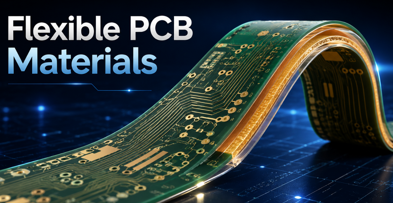
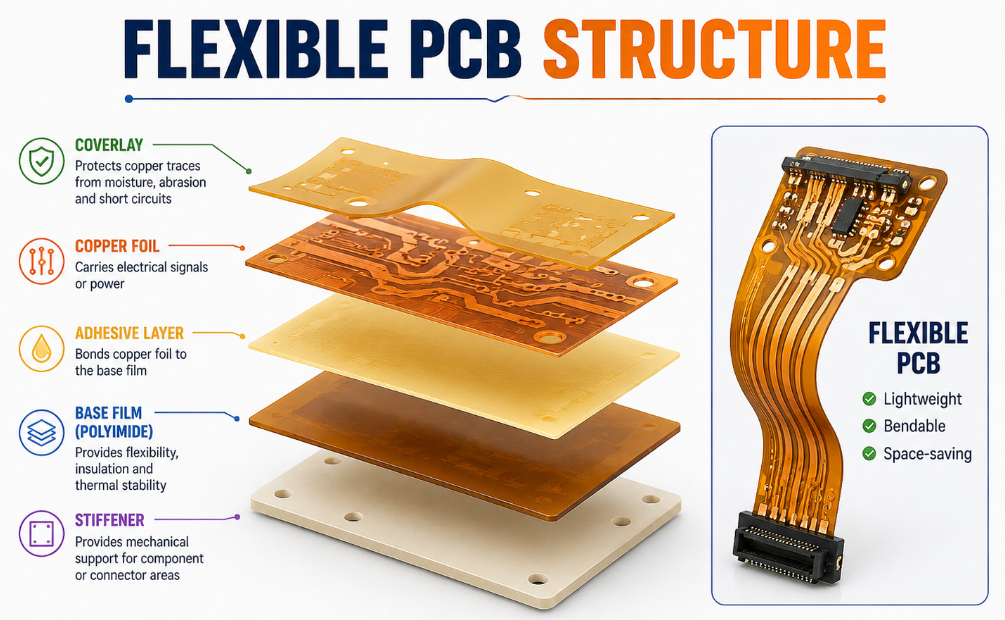
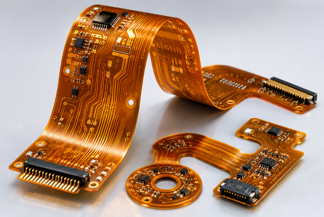
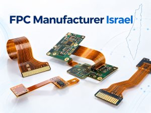
Flexible PCB materials are used to build circuits that can bend, fold, twist, and fit into compact electronic products without losing electrical performance. A flexible PCB usually uses a thin flexible base film, copper foil, adhesive or adhesiveless bonding layers, coverlay, stiffeners, and surface finishes. These materials directly affect bend radius, dynamic flex life, soldering reliability, insulation strength, thickness control, and long-term durability in real applications.

flexible PCB materials, https://www.bestpcbs.com/blog/2026/06/flexible-pcb-materials/

What Are Flexible PCB Materials?

Flexible PCB materials are the base films, conductive foils, adhesives, coverlays, stiffeners, and surface finishes used to manufacture flexible printed circuits. Unlike rigid FR4 boards, flexible PCBs are designed to support movement, space saving, lightweight structure, and three-dimensional assembly.

The most common flexible PCB material stack includes polyimide film, copper foil, adhesive or adhesiveless laminate, coverlay, solder mask, stiffener, and surface finish. Each material has a different function. The base film provides flexibility and insulation, copper carries signals or power, and coverlay protects the circuit.

For product development, choosing the right flexible PCB materials is not only a material decision. It affects mechanical reliability, electrical stability, manufacturing yield, assembly quality, and final product lifetime.

Why Are Flexible PCB Materials Important?

Flexible PCB materials are important because flexible circuits often work in tight spaces, moving areas, or products with strict size and weight limits. If the wrong material is selected, the circuit may suffer from copper cracking, delamination, poor solderability, insulation failure, short flex life, or unstable signal transmission.

A flexible PCB may look thin and simple, but its reliability depends heavily on the material stack. The base film, copper type, adhesive system, coverlay thickness, stiffener location, and surface finish must match the product’s bending condition and assembly process.

In mass production, material consistency is also critical. A small change in adhesive thickness, copper type, or coverlay opening may affect bend performance, impedance, dimensional accuracy, and component assembly quality.

How Do Flexible PCB Materials Work?

Flexible PCB materials work by combining a flexible insulating substrate with copper conductors and protective layers. The base film supports bending, the copper foil carries electrical current or signals, and the coverlay protects the traces from moisture, abrasion, and short circuits.

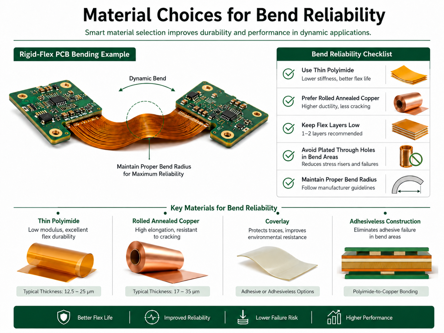
When a flexible PCB bends, the material stack experiences mechanical stress. The copper layer is usually the most vulnerable part because repeated bending can cause fatigue. That is why copper type, copper thickness, bend radius, and trace direction are important.

For high-reliability designs, flexible PCB materials must balance flexibility, adhesion, insulation, heat resistance, soldering compatibility, and dimensional stability. A good material stack allows the board to bend without damaging the circuit.

What Is the Structure of a Flexible PCB?

A typical flexible PCB includes base film, copper foil, adhesive or adhesiveless laminate, coverlay, surface finish, and optional stiffeners. The structure may change depending on whether the board is single-sided, double-sided, multilayer, or rigid-flex.

LayerMain FunctionKey Selection Points
Polyimide base filmSupports flexibility and insulationThickness, heat resistance, dimensional stability
Copper foilCarries current and signalsCopper type, thickness, bend life
Adhesive layerBonds copper to base filmFlexibility, thermal resistance, bonding strength
CoverlayProtects copper tracesThickness, opening accuracy, insulation
Surface finishProtects exposed padsSolderability, shelf life, assembly compatibility
StiffenerSupports component or connector areasMaterial, thickness, bonding method

For most flexible circuits, the base film, copper foil, and coverlay determine the core mechanical reliability. Stiffeners are added only where extra support is needed, such as connector zones or component mounting areas.

flexible PCB structure, https://www.bestpcbs.com/blog/2026/06/flexible-pcb-materials/

What Base Films Are Used in Flexible PCB Materials?

The base film is the foundation of a flexible PCB. It provides electrical insulation and mechanical flexibility. The most common base material is polyimide, while polyester and other films may be used in cost-sensitive or special applications.

Base FilmMain FeaturesCommon Use
PolyimideHigh heat resistance, excellent flexibility, strong insulationMost flexible PCB applications
PolyesterLower cost, good flexibility, lower heat resistanceSimple low-cost circuits
LCPLow moisture absorption, good high-frequency performanceRF, antenna, high-speed applications
PENBetter heat resistance than PET, lower than PISelected flexible electronics

Polyimide is widely used because it handles soldering heat better and supports stronger long-term reliability. For dynamic bending, compact electronics, and industrial products, polyimide is usually the preferred flexible PCB base material.

What Copper Foils Are Used in Flexible PCB Materials?

Copper foil is the conductive layer of a flexible PCB. It forms traces, pads, ground areas, and signal paths. The two common copper types are rolled annealed copper and electrodeposited copper.

Copper TypeTypical FeaturesBest Use
Rolled annealed copperBetter ductility and flex fatigue resistanceDynamic bending and repeated flexing
Electrodeposited copperCost-effective and widely availableStatic flex or limited bending
Heavy copperHigher current capacityPower flexible circuits
Thin copperBetter flexibility and fine tracesCompact and fine-pitch designs

Rolled annealed copper is often selected for applications that require repeated bending because it has better grain structure for flexing. Electrodeposited copper is common in applications where the circuit bends during installation but does not move repeatedly afterward.

What Adhesive Materials Are Used in Flexible PCB Materials?

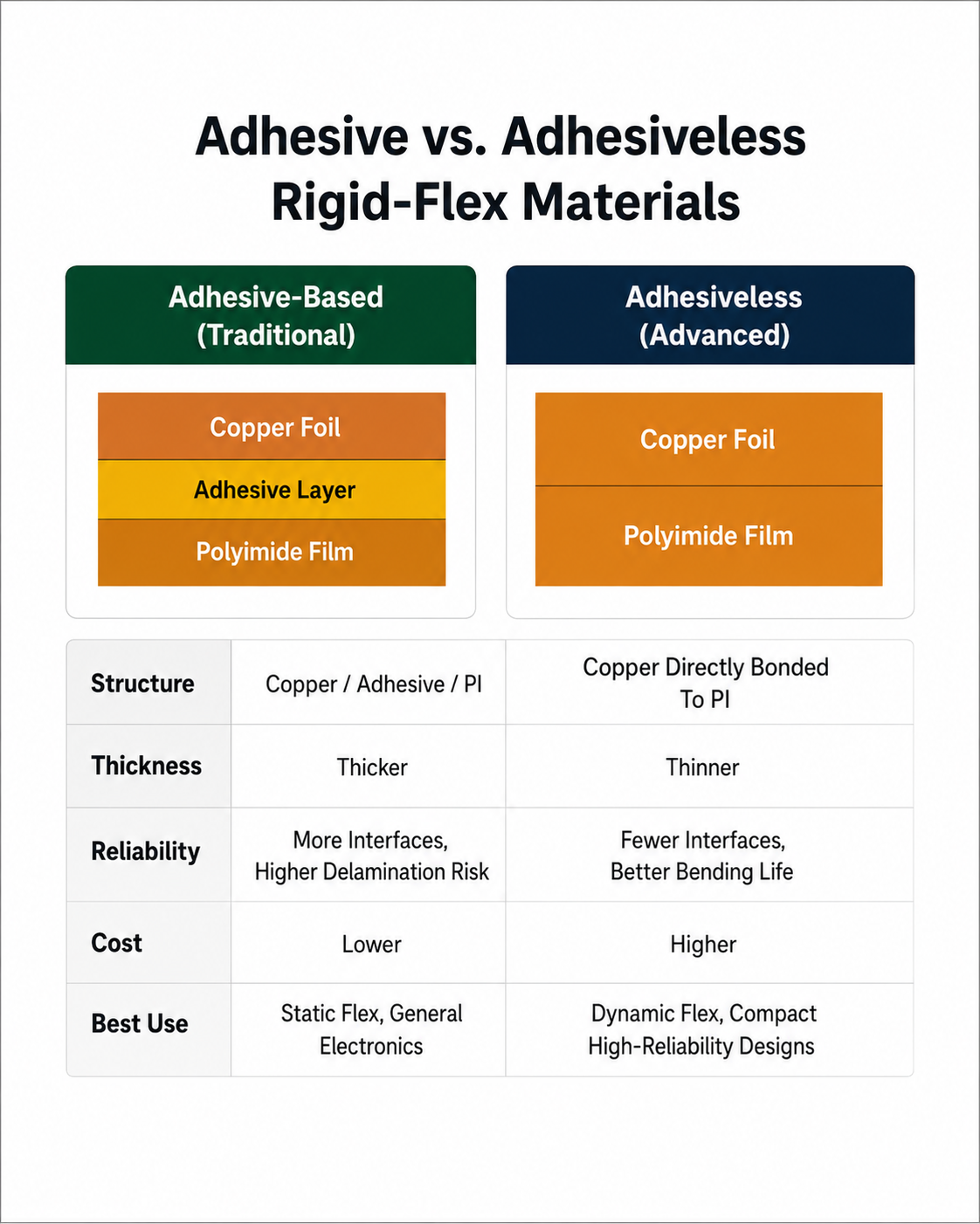
Adhesive materials bond copper foil to the base film and help build the flexible laminate. Flexible PCBs may use adhesive-based materials or adhesiveless materials depending on reliability, thickness, and thermal requirements.

Material TypeAdvantagesLimitations
Adhesive-based laminateCost-effective, widely used, good bondingThicker stack, lower heat resistance than adhesiveless
Adhesiveless laminateThinner, better thermal performance, improved flex lifeHigher cost, tighter process control required
Acrylic adhesiveGood flexibility and bondingMay have lower heat resistance
Epoxy adhesiveGood strength and stabilityMay be less flexible in repeated bending

Adhesiveless flexible PCB materials are often preferred for high-reliability or fine-line circuits because they reduce thickness and improve bend performance. Adhesive-based materials remain practical for many standard applications where cost control matters.

What Coverlay Materials Are Used in Flexible PCBs?

Coverlay is a protective layer used over copper traces on flexible PCBs. It usually consists of polyimide film with adhesive. Coverlay protects the circuit from scratches, moisture, dust, solder bridging, and mechanical damage.

Unlike standard solder mask on rigid PCBs, coverlay is more flexible and better suited for bending areas. It is especially important in circuits that move, fold, or pass through narrow mechanical spaces.

Coverlay FactorWhy It Matters
Coverlay thicknessAffects flexibility and protection
Adhesive thicknessAffects bending and bonding reliability
Opening accuracyControls pad exposure and assembly quality
Heat resistanceSupports soldering and long-term operation
FlexibilityPrevents cracking during bending

Coverlay openings must be designed carefully. If openings are too small, soldering may be difficult. If openings are too large, traces may lose protection near pads or bending areas.

What Stiffener Materials Are Used in Flexible PCB Materials?

Stiffeners are added to selected areas of a flexible PCB to provide mechanical support. They are not part of the electrical circuit, but they improve assembly, connector insertion, and component stability.

Common stiffener materials include FR4, polyimide, stainless steel, aluminum, and pressure-sensitive adhesive-backed materials. The choice depends on the required thickness, rigidity, temperature resistance, and assembly method.

Stiffener MaterialCommon Use
FR4 stiffenerComponent mounting, connector support
Polyimide stiffenerFlexible support with better heat resistance
Stainless steel stiffenerStrong mechanical support in thin areas
Aluminum stiffenerLightweight support and heat spreading
PSA-backed stiffenerFast bonding for selected applications

Stiffeners should be placed only where needed. A poorly designed stiffener edge can create stress concentration and cause cracking near bending zones.

What Surface Finishes Are Used with Flexible PCB Materials?

Surface finish protects exposed copper pads and supports soldering. Common flexible PCB surface finishes include ENIG, OSP, immersion tin, immersion silver, HASL, and hard gold.

Surface FinishMain AdvantagesCommon Use
ENIGFlat surface, good shelf life, stable solderingFine pitch, connectors, reliable assembly
OSPThin, economical, good for fast assemblyCost-sensitive flexible circuits
Immersion tinGood solderability and flatnessSelected connector and soldering areas
Immersion silverGood conductivity and solderabilityHigh-performance applications
HASLCost-effectiveLess common for very thin flex
Hard goldWear resistanceContact fingers and repeated mating areas

ENIG is often used for flexible PCBs because it provides flat pads and reliable solderability. For contact fingers, hard gold may be required to handle repeated insertion or wear.

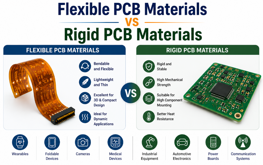
How Do Flexible PCB Materials Compare with Rigid PCB Materials?

Flexible PCB materials and rigid PCB materials are used for different mechanical needs. Rigid boards provide strong structural support, while flexible materials allow bending, folding, and compact installation.

Comparison ItemFlexible PCB MaterialsRigid PCB Materials
Base materialPolyimide, PET, LCPFR4, high Tg FR4, ceramic, metal core
Mechanical behaviorBendable and lightweightRigid and stable
Space savingExcellentLimited in 3D layouts
Assembly supportMay require stiffenersStrong by default
CostOften higher than simple FR4Lower for standard boards
Best useCompact, moving, foldable productsMain control boards and structural circuits
Design riskBend cracking and delaminationWarpage, cracking, thermal stress

Flexible PCB materials are ideal when the product needs movement or compact packaging. Rigid PCB materials are better when the board must support heavy components, connectors, or mechanical loads.

Flexible PCB Materials vs Rigid PCB Materials, https://www.bestpcbs.com/blog/2026/06/flexible-pcb-materials/

How Do Flexible PCB Materials Compare with Rigid-Flex PCB Materials?

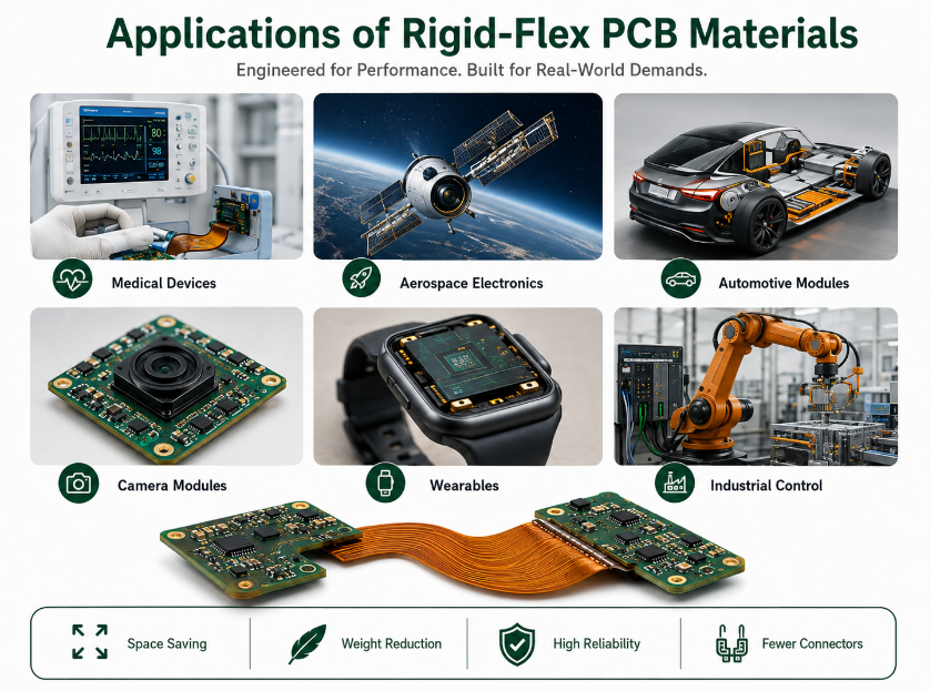
Flexible PCB materials are used in both flexible circuits and rigid-flex boards. The difference is that rigid-flex boards combine flexible sections with rigid PCB sections into one integrated structure.

Comparison ItemFlexible PCBRigid-Flex PCB
StructureFlexible circuit onlyRigid sections plus flexible sections
AssemblyOften needs connectors or stiffenersReduces connectors and cables
CostLower than rigid-flex in many casesHigher manufacturing cost
ReliabilityGood when designed correctlyBetter for complex compact assemblies
Space useVery goodExcellent in 3D products
Best useSimple bending or cable replacementHigh-reliability compact electronics

Rigid-flex PCB is usually selected when the product needs fewer connectors, higher assembly reliability, and compact three-dimensional packaging. Flexible PCB is often better when the design needs a simpler bendable circuit at lower cost.

What Bend Radius Should Be Considered for Flexible PCB Materials?

Bend radius is one of the most important factors for flexible PCB material selection. A smaller bend radius creates higher stress on copper traces and coverlay. If the bend radius is too tight, the flexible PCB may crack or delaminate.

The required bend radius depends on copper thickness, number of layers, base film thickness, adhesive type, coverlay thickness, and whether the bend is static or dynamic. Dynamic bending usually requires a larger bend radius and more careful material selection.

For safer design, traces should be routed perpendicular to the bend direction when possible, and copper should be kept away from sharp bend edges. The bend area should be as simple, thin, and stress-free as possible.

What Electrical Properties Should Be Checked?

Flexible PCB materials must provide stable electrical performance while bending or fitting into compact spaces. Important properties include dielectric strength, insulation resistance, impedance control, copper thickness, current capacity, dielectric constant, and moisture resistance.

Electrical PropertyWhy It Matters
Dielectric strengthPrevents insulation breakdown
Insulation resistanceReduces leakage current
Copper thicknessSupports current capacity
Dielectric constantAffects high-speed and RF signals
Impedance controlSupports stable signal transmission
Moisture resistanceImproves reliability in humid environments

For high-speed, RF, or antenna applications, LCP or special low-loss materials may be considered. For standard industrial products, polyimide-based flexible PCB materials are often sufficient.

What Manufacturing Processes Are Used for Flexible PCBs?

Flexible PCB manufacturing includes material cutting, drilling, imaging, etching, coverlay lamination, surface finishing, electrical testing, profiling, stiffener bonding, and final inspection. The process requires careful handling because flexible materials are thin and easily deformed.

Common production steps include laminate preparation, copper patterning, drilling or laser processing, coverlay alignment, lamination, surface finish, outline cutting, electrical test, and packaging.

Manufacturing quality depends on precise control of coverlay openings, dimensional stability, adhesive flow, copper adhesion, and surface cleanliness. Poor process control may cause misalignment, wrinkles, delamination, or poor soldering results.

What Quality Tests Are Needed for Flexible PCB Materials?

Flexible PCB materials should be tested for mechanical, electrical, thermal, and assembly reliability. Quality control should check not only the circuit, but also the flexibility, adhesion, coverlay bonding, and dimensional stability.

Test ItemPurpose
Visual inspectionChecks scratches, stains, coverlay defects, and exposed copper
Electrical testConfirms open and short performance
Dimensional inspectionChecks outline, hole size, and pad position
Peel strength testConfirms copper adhesion
Bend testEvaluates flex performance
Solderability testConfirms assembly readiness
Thermal stress testChecks heat resistance
Insulation resistance testConfirms electrical isolation

For moving applications, bend testing is especially important. Static bend and dynamic bend requirements should be clearly defined before production.

What Common Problems Happen with Flexible PCB Materials?

Common problems include copper cracking, coverlay delamination, adhesive overflow, poor solderability, pad lifting, stiffener misalignment, trace fracture, impedance instability, and insulation failure.

Copper cracking often happens when the bend radius is too small, copper is too thick, or the wrong copper type is used. Delamination may come from weak bonding, moisture, poor lamination, or repeated thermal cycling. Stiffener misalignment can affect connector insertion and assembly accuracy.

Many failures can be avoided by reviewing the material stack early. The design should match bend type, bend radius, copper thickness, coverlay structure, stiffener placement, and assembly temperature.

How to Choose the Right Flexible PCB Materials?

Choosing the right flexible PCB materials starts with the product’s movement and environment. Confirm whether the board will be bent once during installation or flexed repeatedly during use. Then check thickness, copper type, base film, coverlay, stiffener, surface finish, and reliability requirements.

For dynamic bending, choose polyimide, rolled annealed copper, thinner copper, thinner dielectric, and smooth bend routing. For static bending, electrodeposited copper or adhesive-based materials may be suitable if the design is not highly stressed.

For high-temperature, automotive, medical, or industrial products, material selection should also consider thermal cycling, humidity, vibration, soldering process, chemical exposure, and lifetime expectations.

What Factors Affect the Cost of Flexible PCB Materials?

Flexible PCB material cost depends on base film type, copper type, copper thickness, layer count, adhesive type, coverlay thickness, surface finish, stiffeners, tolerance, testing, and order quantity.

Cost FactorWhy It Affects PriceCost Control Suggestion
Base filmPolyimide and LCP cost more than PETMatch material to real application needs
Copper typeRolled annealed copper costs more than ED copperUse RA copper where dynamic bending is required
Layer countMore layers increase lamination complexityKeep flex areas simple where possible
Adhesiveless laminateImproves performance but increases costUse for high-reliability or thin designs
Surface finishENIG and hard gold cost moreChoose by assembly and contact needs
StiffenersAdd material and bonding stepsUse only where mechanical support is needed
TestingBend and reliability tests add costApply critical tests to high-risk applications

A low-cost flexible material may not be cheaper if it causes field failure. Cost control should focus on correct material selection, simplified bend zones, and stable manufacturability.

Where Are Flexible PCB Materials Commonly Used?

Flexible PCB materials are used in products that require lightweight circuits, movement, compact structure, or repeated bending.

Consumer electronics: smartphones, tablets, cameras, wearables, foldable devices, and display modules.

Automotive electronics: sensors, lighting, battery systems, dashboards, cameras, and control modules.

Medical devices: diagnostic equipment, wearable monitors, imaging devices, probes, and compact instruments.

Industrial equipment: sensors, robotic arms, control modules, HMI systems, and moving machine assemblies.

Aerospace and defense electronics: lightweight assemblies, compact modules, and high-reliability interconnects.

Communication products: antennas, RF modules, optical modules, and compact signal interconnects.

What Should You Confirm Before Ordering Flexible PCBs?

Before ordering flexible PCBs, confirm material stack, base film thickness, copper type, copper thickness, coverlay thickness, bend radius, surface finish, stiffener material, tolerance, and testing requirements.

You should also provide Gerber files, drill files, stack-up notes, drawings, bend area requirements, stiffener drawings, BOM if assembly is needed, quantity, and final application details.

For dynamic bending or high-reliability products, prototype validation is recommended before mass production. Testing under real bending, temperature, and assembly conditions helps reduce batch risk.

Why Choose EBest for Flexible PCB Manufacturing?

EBest Technology provides one-stop PCB solutions, including PCB design, PCB prototype, mass production, component sourcing, PCB assembly, and box-build assembly. Its product range includes standard FR4 PCB, multilayer PCB, metal-based PCB, ceramic PCB, flexible PCB, rigid-flex PCB, and high frequency PCB, supporting customers with different electronic manufacturing needs.

For flexible PCB projects, EBest can support material selection, stack-up review, prototype validation, batch production, assembly coordination, and quality inspection. This is useful when a project involves compact routing, connector areas, stiffeners, bend zones, and final product assembly.

EBest also supports quality and compliance systems such as IATF 16949, ISO 9001:2015, ISO 13485:2016, AS9100D, REACH, RoHS, and UL-related requirements. These capabilities help customers manage industrial, automotive, medical, aerospace, and export-oriented projects with more confidence.

flexible PCB, https://www.bestpcbs.com/blog/2026/06/flexible-pcb-materials/

FAQs About Flexible PCB Materials

Q1: What are flexible PCB materials made of?
A1: Flexible PCB materials usually include polyimide base film, copper foil, adhesive or adhesiveless bonding layers, coverlay, surface finish, and optional stiffeners. These materials work together to provide flexibility, insulation, electrical connection, mechanical support, and circuit protection.

Q2: What is the most common flexible PCB base material?
A2: Polyimide is the most common base material because it offers excellent heat resistance, strong insulation, good flexibility, and stable long-term performance. It is widely used in consumer electronics, automotive systems, medical devices, and industrial electronics.

Q3: What copper type is best for flexible PCB materials?
A3: Rolled annealed copper is often better for dynamic bending because it has stronger flex fatigue resistance. Electrodeposited copper is more cost-effective and suitable for static flex or applications where the board bends only during installation.

Q4: What is the difference between coverlay and solder mask?
A4: Coverlay is a flexible protective film, usually made from polyimide and adhesive. It is better for bending areas. Solder mask is more common on rigid PCBs and may not provide the same flexibility for repeated bending applications.

Q5: Are adhesiveless flexible PCB materials better?
A5: Adhesiveless materials can provide thinner structure, better thermal performance, improved dimensional stability, and better flex life. They are often used for high-reliability, fine-line, or dynamic bending applications, but they usually cost more.

Q6: How do I choose flexible PCB material thickness?
A6: Material thickness depends on bend radius, layer count, current load, mechanical space, and assembly needs. Thinner materials generally bend better, while thicker materials may provide stronger support but increase bending stress.

Q7: What causes copper cracking in flexible PCBs?
A7: Copper cracking may happen when the bend radius is too small, copper is too thick, the wrong copper type is used, or traces are placed poorly in the bend area. Proper material selection and bend design help prevent this issue.

Q8: Can flexible PCB materials support high-speed signals?
A8: Yes. Flexible PCBs can support high-speed signals when material dielectric properties, impedance control, copper roughness, trace geometry, and stack-up are properly designed. LCP or low-loss materials may be used for demanding RF applications.

Q9: Why are stiffeners used in flexible PCBs?
A9: Stiffeners provide mechanical support in selected areas, such as connectors, soldering zones, and component mounting locations. They help improve assembly stability but should not be placed in active bending zones unless carefully designed.

Q10: What surface finish is best for flexible PCBs?
A10: ENIG is commonly selected because it provides flat pads, good shelf life, and reliable soldering. OSP may be used for cost-sensitive and fast assembly projects, while hard gold is used for contact fingers or wear-resistant areas.

Q11: Are flexible PCB materials suitable for medical devices?
A11: Yes. Flexible PCB materials are widely used in medical devices because they support compact size, lightweight structure, and flexible interconnection. Material selection should consider reliability, cleanliness, insulation, biocompatible packaging, and long-term operating conditions.

Q12: What files are needed for a flexible PCB quotation?
A12: Provide Gerber files, drill files, stack-up requirements, copper thickness, base material, coverlay information, stiffener drawing, surface finish, quantity, bend radius requirements, and application details. For assembly, also provide BOM and placement files.

Conclusion

Flexible PCB materials determine how well a circuit can handle bending, insulation, soldering, current, thermal stress, dimensional control, and long-term reliability. The right material stack should be selected based on the real bending condition, operating environment, assembly process, and product lifetime target.

For product development, do not choose flexible PCB materials only by price or thickness. Review base film, copper type, adhesive system, coverlay, stiffener placement, surface finish, bend radius, and testing requirements before confirming the stack-up. For procurement, work with a manufacturer that can support prototype review, batch consistency, quality inspection, assembly coordination, and reliable delivery.

If you need flexible PCB materials, flexible PCB manufacturing, PCB assembly, OEM production, ODM development, sample testing, batch production, or custom engineering solutions, please contact our team at sales@bestpcbs.com for technical support and quotation service.
You may also like

Copper Base PCB Materials

June 4th, 2026

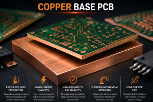
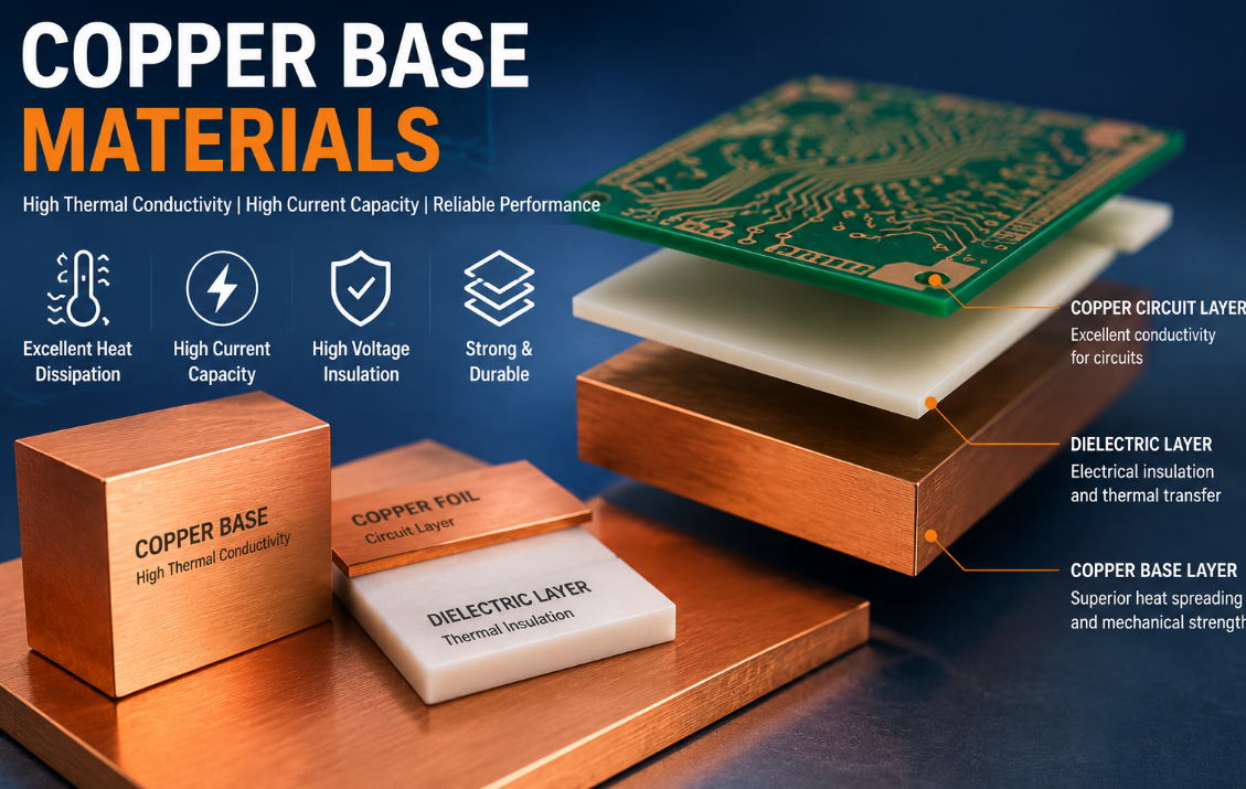
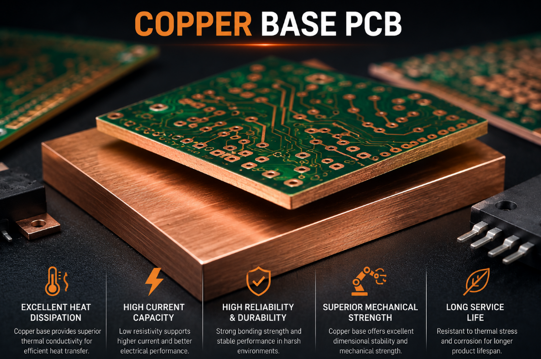
Copper base PCB materials are used for circuit boards that need strong thermal conductivity, high current capacity, mechanical stability, and reliable operation under heat stress. Compared with standard FR4 and aluminum-based boards, copper base PCBs provide better heat spreading because copper has excellent thermal and electrical performance. They are commonly used in power electronics, high-power LED modules, automotive lighting, charging systems, motor drives, industrial controls, and thermal management applications.

Copper Base PCB Materials

What Are Copper Base PCB Materials?

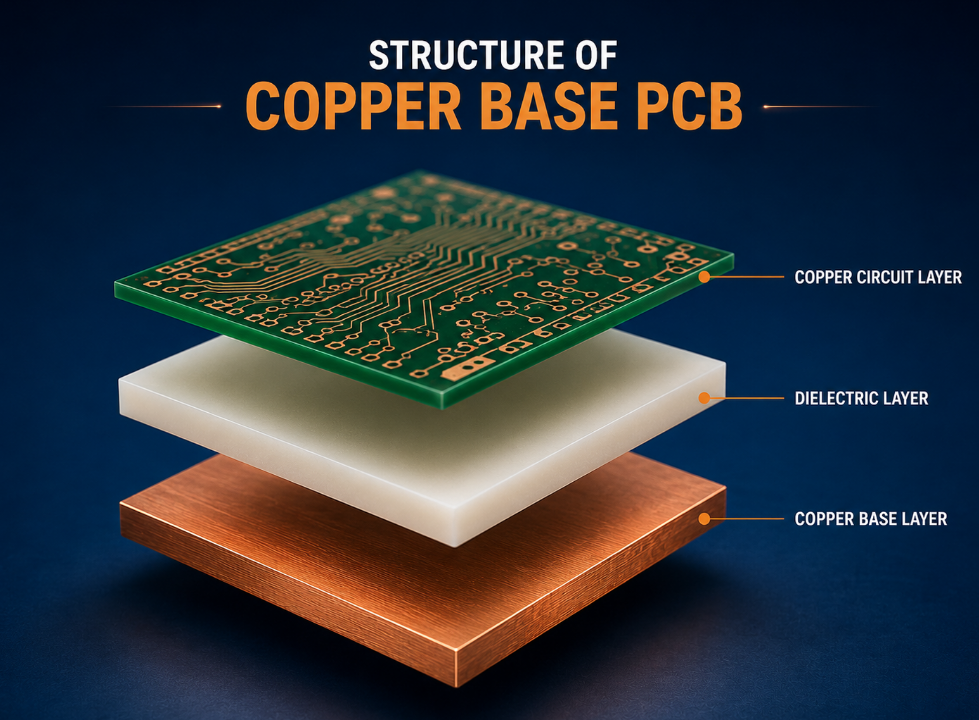
Copper base PCB materials refer to the material stack used to build a copper metal core PCB. A typical structure includes a copper circuit layer, a thermally conductive dielectric layer, and a copper base substrate. The copper circuit layer carries electrical signals or power, the dielectric layer provides insulation and heat transfer, and the copper base spreads heat away from components.

Unlike a standard FR4 PCB, a copper base PCB is designed mainly for thermal management and high-power reliability. The copper base acts as a strong heat spreader, helping reduce hot spots around LEDs, MOSFETs, IGBTs, power modules, and other heat-generating components.

For industrial projects, choosing the right copper base PCB materials affects thermal resistance, breakdown voltage, soldering reliability, board flatness, mechanical strength, surface finish quality, and long-term service life.

Why Are Copper Base PCB Materials Important?

Copper base PCB materials are important because high-power electronics often fail when heat cannot be removed fast enough. Excessive heat may cause component aging, solder joint fatigue, dielectric breakdown, copper delamination, unstable output, and reduced product lifetime.

Copper has better thermal conductivity than aluminum, which makes copper base PCBs useful when the design has higher heat density, smaller space, higher current, or stricter temperature limits. This is especially valuable for power modules, LED lighting, automotive electronics, and industrial power control systems.

In batch production, material consistency is also critical. A copper base PCB may look simple, but small differences in dielectric thickness, copper base quality, copper foil thickness, surface finish, and lamination control can affect real thermal performance.

How Do Copper Base PCB Materials Work?

Copper base PCB materials work by building a fast heat transfer path from the component to the copper base. Heat moves from the component pad into the copper circuit layer, passes through the thermally conductive dielectric layer, and spreads into the copper substrate.

The dielectric layer is the key bridge between electrical insulation and thermal transfer. It must isolate the copper circuit from the copper base while still allowing heat to pass efficiently. If the dielectric layer is too thick or has poor thermal conductivity, the board may not perform as expected.

The copper base then spreads heat across a larger area. This helps reduce local hot spots and supports better contact with a heatsink, metal housing, cooling plate, or thermal interface material. In real products, performance also depends on component layout, copper pad size, mounting pressure, solder quality, airflow, and enclosure design.

What Is the Structure of a Copper Base PCB?

A common copper base PCB has three main functional layers: copper circuit layer, dielectric insulation layer, and copper base layer. Some designs also include solder mask, surface finish, silkscreen, plated holes, and protective coating.

LayerMain FunctionKey Selection Points
Copper circuit layerCarries current and forms pads/tracesCopper thickness, trace width, current capacity
Dielectric layerProvides insulation and heat transferThermal conductivity, breakdown voltage, thickness
Copper base layerSpreads heat and supports the boardCopper grade, thickness, flatness, thermal performance
Solder maskProtects copper circuitsHeat resistance, adhesion, insulation, color
Surface finishProtects exposed copper padsSolderability, shelf life, assembly compatibility

For high-power products, the dielectric layer and copper base thickness are often the most important material choices. They directly affect heat flow, voltage safety, and long-term reliability.

copper base PCB structure

What Types of Copper Base PCB Materials Are Common?

Copper base PCB materials can be divided by structure, thermal performance, copper thickness, insulation type, and application requirement. The most common types include standard copper base materials, high thermal conductivity copper base materials, high-voltage insulation copper base materials, and heavy copper copper-base materials.

Standard copper base materials are used for power boards, LED modules, and industrial products that need better thermal performance than aluminum or FR4.

High thermal conductivity materials are used in compact power electronics, high-brightness LED modules, and products where heat concentration is severe.

High-voltage insulation materials are selected when the circuit must pass voltage withstand testing or operate under higher voltage stress.

Heavy copper copper-base materials are used for high-current circuits, power conversion, charging systems, motor drivers, and energy control products where both current and heat are major concerns.

What Copper Base Materials Are Used in Copper Base PCBs?

The copper base is usually made from high-purity copper or copper alloy depending on thermal performance, mechanical strength, machinability, and cost. Common choices include C1100 copper, C1020 oxygen-free copper, T2 copper, and selected copper alloys.

Copper Base TypeTypical FeaturesCommon Use
C1100 copperHigh thermal and electrical conductivityPower boards, LED thermal boards
C1020 oxygen-free copperHigh purity, stable conductivity, low oxygen contentHigh-reliability thermal applications
T2 copperGood conductivity, common industrial availabilityGeneral copper base PCB projects
Copper alloyBetter mechanical strength, lower conductivity than pure copperStructural or special mechanical applications

For most thermal PCB projects, the copper base is selected for heat spreading, flatness, thickness stability, machining quality, and bonding reliability. If the board must contact a heatsink or housing, surface flatness becomes especially important.

What Dielectric Materials Are Used in Copper Base PCB Materials?

The dielectric layer is usually a ceramic-filled thermally conductive polymer system. It must provide electrical insulation while transferring heat from the copper circuit layer to the copper base. This layer is often more important than the copper base itself because it controls the main thermal bottleneck.

Important dielectric properties include thermal conductivity, dielectric breakdown voltage, thickness, adhesion strength, glass transition temperature, thermal aging resistance, and moisture resistance.

Dielectric PropertyWhy It Matters
Thermal conductivityControls heat transfer from circuit layer to copper base
Dielectric strengthPrevents electrical breakdown between circuit and base
ThicknessAffects both heat transfer and insulation safety
Adhesion strengthReduces delamination risk during thermal cycling
Heat resistanceImproves reliability during soldering and operation
Moisture resistanceProtects insulation under humid conditions

A common selection mistake is focusing only on copper thickness while ignoring dielectric performance. In real operation, a poor dielectric layer can limit the full advantage of a copper base PCB.

What Copper Thickness Is Used in Copper Base PCB Materials?

Copper thickness affects current capacity, heat spreading, etching accuracy, soldering performance, and cost. Common copper foil thicknesses include 1 oz, 2 oz, 3 oz, 4 oz, and heavier copper options. The copper base itself may be much thicker, often selected based on mechanical and thermal needs.

Copper ThicknessTypical UseKey Consideration
1 ozLED and general control circuitsGood for standard current and finer traces
2 ozPower supplies and LED driversBetter current capacity and heat spreading
3 oz to 4 ozHigh-current power boardsRequires wider spacing and stronger etching control
Heavy copperMotor drives, chargers, energy systemsHigher cost and more complex processing

For high-current designs, copper thickness should be selected together with trace width, temperature rise target, insulation distance, solder mask capability, and assembly process. More copper is helpful, but overusing heavy copper can increase cost and manufacturing difficulty.

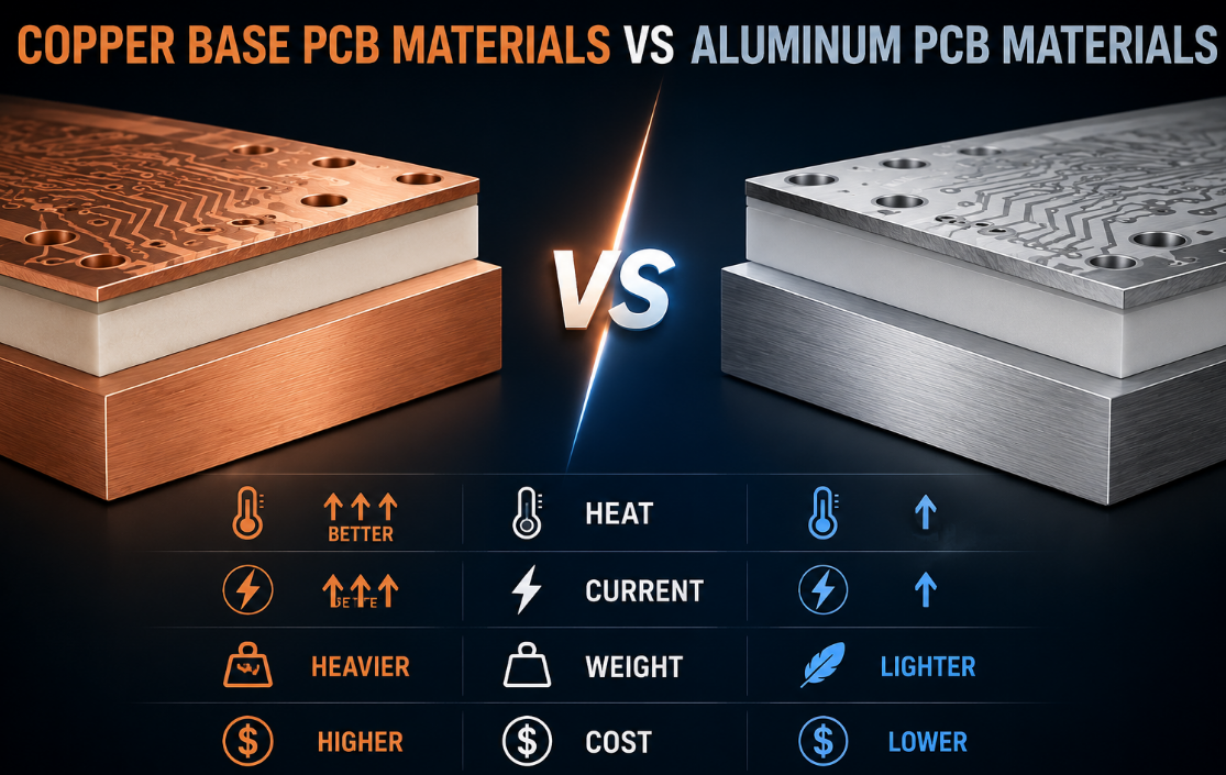
How Do Copper Base PCB Materials Compare with Aluminum PCB Materials?

Copper base PCB materials and aluminum PCB materials are both metal core solutions, but they are used for different thermal and cost targets.

Comparison ItemCopper Base PCB MaterialsAluminum PCB Materials
Thermal conductivityHigher heat spreading performanceGood but lower than copper
Current capacityBetter for high-current designsSuitable for many LED and power boards
Mechanical weightHeavierLighter
Material costHigherMore cost-effective
Machining difficultyMore demandingEasier and more common
Best useHigh-power, compact, high-heat productsLED lighting, general power products
Cost controlHigher project costBetter for budget-sensitive projects

Copper base PCB materials are usually chosen when heat density is too high for aluminum-based boards. Aluminum PCB materials are still a good choice when the project needs balanced performance and cost.

copper base PCB materials vs aluminum PCB materials

How Do Copper Base PCB Materials Compare with Ceramic PCB Materials?

Copper base PCBs and ceramic PCBs are both used for thermal applications, but their material behavior is different. Copper base boards provide excellent heat spreading and mechanical toughness, while ceramic boards provide strong insulation and high thermal stability.

Comparison ItemCopper Base PCB MaterialsCeramic PCB Materials
Heat spreadingExcellent through copper baseExcellent through ceramic substrate
Electrical insulationDepends on dielectric layerCeramic itself provides insulation
Mechanical behaviorTough and metallicHard but brittle
CostUsually high but practical for many power boardsOften higher for advanced ceramics
Current handlingStrong for high-current circuitsDepends on metallization and structure
Best usePower, LED, automotive, industrial controlRF, laser, medical, aerospace, power modules

Copper base PCBs are often selected when the project needs high thermal spreading, high current, mechanical durability, and practical assembly compatibility. Ceramic PCBs are selected when insulation stability, low expansion, or advanced thermal performance is more critical.

What Thermal Conductivity Is Needed for Copper Base PCB Materials?

The required thermal conductivity depends on component power, temperature limit, board size, copper area, dielectric thickness, cooling method, and operating environment. Copper itself has very high thermal conductivity, but the final PCB performance depends heavily on the dielectric layer.

For many copper base PCB designs, the dielectric layer is the main thermal bottleneck. A thinner high-performance dielectric can improve heat transfer, but it must still meet voltage and insulation requirements.

The better way to select materials is to evaluate total thermal resistance, not only the thermal conductivity of one layer. The full stack-up, component layout, soldering quality, contact surface, and heatsink design all influence the final temperature.

What Electrical Properties Should Be Checked?

Copper base PCB materials must provide reliable current carrying ability and electrical insulation. Because the copper base is conductive, the dielectric layer must safely isolate the circuit layer from the metal substrate.

Important electrical properties include breakdown voltage, insulation resistance, creepage and clearance distance, copper thickness, current capacity, leakage risk, and voltage withstand testing performance.

Electrical PropertyWhy It Matters
Breakdown voltagePrevents insulation failure between circuit and copper base
Insulation resistanceReduces leakage current risk
Copper thicknessSupports current carrying capacity
Creepage and clearanceImproves safety for high-voltage designs
Hi-pot performanceConfirms insulation reliability before shipment
Surface finish qualitySupports stable soldering and electrical contact

A copper base PCB can conduct heat very well, but it can fail if the insulation system is not suitable. For high-power designs, thermal and electrical requirements must be reviewed together.

What Surface Finishes Are Used with Copper Base PCB Materials?

Surface finish protects exposed copper pads and supports soldering. Common surface finishes include HASL, lead-free HASL, ENIG, OSP, immersion tin, and immersion silver. The right choice depends on component type, pad flatness, shelf life, soldering process, and cost.

Surface FinishAdvantagesCommon Use
HASLCost-effective and widely usedGeneral power and LED boards
Lead-free HASLRoHS-friendly solderabilityExport and compliant products
ENIGFlat surface, good shelf life, stable solderingPrecision assembly and high-reliability boards
OSPClean and economicalShort storage and fast assembly
Immersion tinGood flatness and solderabilitySelected power and connector designs
Immersion silverGood conductivity and solderabilityHigh-performance applications

For copper base boards with high current or high power density, surface finish should be selected with assembly reliability in mind. ENIG is often preferred for flatness and stable solder joints, while HASL may be used for cost-sensitive projects.

What Manufacturing Processes Are Used for Copper Base PCBs?

Copper base PCB manufacturing includes material preparation, drilling, imaging, etching, lamination, solder mask printing, surface finishing, profiling, testing, and final inspection. Compared with standard FR4 or aluminum PCBs, copper base PCBs require stronger process control because copper is heavier, softer, more conductive, and more demanding to machine.

Common production steps include cutting copper-clad laminate, drilling mounting holes, forming copper circuits, applying solder mask, processing surface finish, routing board outline, testing insulation, checking flatness, and inspecting appearance.

For thicker copper bases, drilling and profiling quality are especially important. Burrs, scratches, poor bonding, or dielectric damage can affect assembly, insulation, and thermal contact.

What Quality Tests Are Needed for Copper Base PCB Materials?

Copper base PCB materials should be tested for thermal, electrical, mechanical, and assembly reliability. Quality inspection should not only check whether the circuit is open or short. It should also confirm insulation strength, material bonding, flatness, and surface quality.

Test ItemPurpose
Visual inspectionChecks scratches, stains, solder mask defects, and exposed copper
Dimensional inspectionConfirms outline, hole size, thickness, and tolerance
Electrical testVerifies circuit continuity and isolation
Hi-pot testChecks dielectric withstand voltage
Insulation resistance testConfirms electrical isolation stability
Peel strength testChecks copper adhesion and bonding reliability
Flatness inspectionSupports heatsink contact and assembly fit
Thermal cyclingEvaluates material reliability under repeated heating and cooling

For high-power products, thermal testing after assembly is also helpful. Real load testing can reveal whether the selected material stack and cooling design are suitable.

What Common Problems Happen with Copper Base PCB Materials?

Common problems include poor insulation, dielectric breakdown, delamination, board warpage, copper burrs, poor solderability, weak bonding, scratches on copper base, and unstable thermal contact.

Poor insulation may happen if the dielectric layer is too thin, damaged, or unsuitable for the voltage requirement. Delamination may result from weak adhesion, poor lamination, moisture stress, or severe thermal cycling. Burrs around copper edges may affect assembly safety and insulation clearance.

Many failures are caused by the combination of wrong material selection, aggressive thermal load, poor mechanical mounting, unsuitable surface finish, and weak process control. For high-power products, material selection should be verified during prototype testing before full production.

How to Choose the Right Copper Base PCB Materials?

Choosing the right copper base PCB materials starts with the real application. Confirm power level, current load, operating voltage, maximum temperature, board size, component layout, cooling method, insulation requirement, and assembly process.

For LED modules, focus on thermal conductivity, surface reflectivity, dielectric stability, and soldering reliability. For power electronics, focus on copper thickness, current capacity, insulation strength, thermal resistance, and heat cycling reliability. For automotive and industrial applications, focus on temperature cycling, vibration resistance, corrosion protection, and batch consistency.

The best material is not always the most expensive material. The right material is the one that meets thermal, electrical, mechanical, cost, and production requirements at the same time.

What Factors Affect the Cost of Copper Base PCB Materials?

Copper base PCBs are usually more expensive than aluminum PCBs because copper material cost is higher and processing is more demanding. Cost depends on copper base thickness, copper foil thickness, dielectric thermal conductivity, dielectric thickness, surface finish, board size, tolerance, test requirements, and order quantity.

Cost FactorWhy It Affects PriceCost Control Suggestion
Copper base thicknessMore copper increases material costUse thickness based on real thermal need
Heavy copper circuitsRequires more material and process controlMatch copper thickness to current demand
Dielectric gradeHigher thermal and voltage performance costs moreChoose according to real application stress
Surface finishENIG and special finishes cost moreSelect based on assembly and reliability needs
Board outlineComplex routing increases machining timeSimplify unnecessary shapes
TestingHi-pot, thermal cycling, and special tests add costApply critical tests where required
QuantitySmall batches have higher setup costPlan prototype and batch production together

A low-cost material may create higher total cost if it causes overheating, insulation failure, rework, or field complaints. Cost control should focus on safe optimization, not material downgrading.

Where Are Copper Base PCB Materials Commonly Used?

Copper base PCB materials are used in products that require high thermal performance, high current capacity, and reliable long-term operation.

High-power LED lighting: industrial lights, automotive lights, stage lights, UV LED modules, and compact lighting systems.

Power electronics: converters, inverters, power supplies, regulators, charging modules, and MOSFET power boards.

Automotive electronics: headlights, battery control units, charging systems, power distribution boards, and thermal control modules.

Industrial control: motor drives, automation modules, high-current control boards, and machine electronics.

Energy systems: solar inverters, battery packs, energy storage equipment, and charging stations.

Thermal management modules: compact designs where heat must move quickly from the circuit to a metal body or heatsink.

What Should You Confirm Before Ordering Copper Base PCBs?

Before ordering copper base PCBs, confirm copper base thickness, copper foil thickness, dielectric thermal conductivity, dielectric thickness, voltage requirement, operating temperature, surface finish, solder mask color, board outline, tolerance, and inspection standard.

You should also provide complete production files, including Gerber files, drill files, stack-up notes, drawings, material requirements, quantity, surface finish, testing requirements, and application details. For assembly projects, BOM and placement files should also be provided.

For high-power or high-voltage projects, prototype validation is strongly recommended. Testing the board under real load helps confirm whether the material stack, heat path, and mechanical mounting design are suitable before batch production.

Why Choose EBest for Copper Base PCB Manufacturing?

EBest Technology provides one-stop PCB solutions, including PCB design, PCB prototype, mass production, component sourcing, PCB assembly, and box-build assembly. Its product range includes standard FR4 PCB, multilayer PCB, metal-based PCB, ceramic PCB, flexible PCB, rigid-flex PCB, and high frequency PCB, supporting customers with different electronic manufacturing needs.

For copper base PCB projects, EBest can support engineering review, material selection, prototype validation, batch production, assembly coordination, quality inspection, and global delivery. This is useful when a project involves high-power components, thermal design, mechanical housings, connectors, and final product assembly.

EBest also supports quality and compliance systems such as IATF 16949, ISO 9001:2015, ISO 13485:2016, AS9100D, REACH, RoHS, and UL-related requirements. These capabilities help customers manage industrial, automotive, medical, aerospace, and export-oriented projects with more confidence.

copper base PCB

FAQs About Copper Base PCB Materials

Q1: What are copper base PCB materials made of?
A1: Copper Base PCB Materials usually include a copper circuit layer, a thermally conductive dielectric layer, and a copper base substrate. The copper circuit carries current, the dielectric provides insulation and heat transfer, and the copper base spreads heat away from components.

Q2: Why use copper base PCB materials instead of aluminum PCB materials?
A2: Copper base PCB materials are used when a project needs higher thermal spreading, higher current capacity, and stronger heat control than aluminum PCBs can provide. They are common in high-power LED, power electronics, automotive lighting, and industrial control products.

Q3: What is the most important layer in a copper base PCB?
A3: The dielectric layer is often the most critical because it controls both insulation safety and heat transfer. Even with a strong copper base, poor dielectric performance can cause overheating, electrical breakdown, or delamination during long-term operation.

Q4: What copper thickness should I choose for a copper base PCB?
A4: The right copper thickness depends on current load, trace width, temperature rise, and board size. Standard designs may use 1 oz or 2 oz copper, while power boards may require 3 oz, 4 oz, or heavier copper for better current capacity.

Q5: Are copper base PCBs suitable for high-voltage applications?
A5: Yes, but the dielectric layer must have enough breakdown voltage, insulation resistance, and creepage clearance. High-voltage designs should define operating voltage, surge voltage, test voltage, and safety requirements before material selection.

Q6: Are copper base PCBs more expensive than aluminum PCBs?
A6: Yes. Copper base PCBs usually cost more because copper material is more expensive and processing is more demanding. They are usually selected when the project needs higher thermal performance or higher current capability that justifies the cost.

Q7: Can copper base PCB materials be used for LED lighting?
A7: Yes. Copper base PCB materials are suitable for high-power LED lighting, especially when LED density is high or the product has limited cooling space. They help reduce hot spots and support brightness stability and longer service life.

Q8: What surface finish is recommended for copper base PCBs?
A8: Common options include HASL, lead-free HASL, ENIG, OSP, immersion tin, and immersion silver. ENIG is often selected for flat pads, better shelf life, and stable soldering, while HASL may be used for cost-sensitive designs.

Q9: Why do copper base PCBs delaminate?
A9: Delamination may happen because of weak bonding, poor dielectric material, moisture stress, high soldering temperature, or repeated thermal cycling. Proper material selection, lamination control, and thermal design help reduce this risk.

Q10: What tests are needed for copper base PCBs?
A10: Important tests include electrical test, hi-pot test, insulation resistance test, dimensional inspection, visual inspection, peel strength test, flatness inspection, and thermal cycling. For high-power boards, real load thermal testing is also recommended.

Q11: Can copper base PCBs support PCB assembly?
A11: Yes. Copper base PCBs can support SMT assembly and selected through-hole assembly, depending on design structure. Assembly planning should consider heat absorption, soldering profile, component placement, surface finish, and board flatness.

Q12: What files are needed for a copper base PCB quotation?
A12: Provide Gerber files, drill files, copper thickness, copper base thickness, dielectric requirements, surface finish, solder mask color, board thickness, quantity, drawings, voltage requirement, and application details. For assembly, also provide BOM and placement files.

Conclusion

Copper base PCB materials are used when a circuit board needs strong heat spreading, high current capacity, reliable insulation, and stable long-term performance. The key is not only choosing a copper base, but also selecting the right dielectric layer, copper foil thickness, surface finish, and testing requirements.

For engineering projects, do not choose materials by thermal conductivity alone. Review thermal resistance, voltage safety, current load, mounting method, operating environment, and production consistency before confirming the stack-up. For procurement, work with a manufacturer that can support material review, prototype testing, batch control, assembly coordination, and reliable delivery.

If you need copper base PCB materials , copper base PCB manufacturing, PCB assembly, OEM production, ODM development, sample testing, batch production, or custom engineering solutions, please contact our team at sales@bestpcbs.com for technical support and quotation service.
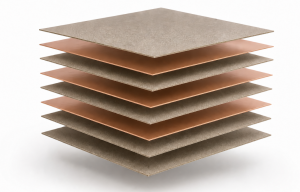
You may also like

Aluminum PCB Materials

June 4th, 2026

Aluminum PCB Materials are used to build metal core circuit boards that need better heat dissipation, mechanical strength, and long-term thermal reliability. Unlike standard FR4 boards, an aluminum PCB uses an aluminum base, a thermally conductive dielectric layer, and a copper circuit layer to move heat away from power components. This structure makes it suitable for LED lighting, power modules, automotive electronics, motor drives, industrial controls, and high-current applications where heat must be controlled from the beginning of the design.

aluminum PCB materials, https://www.bestpcbs.com/blog/2026/06/aluminum-pcb-materials/

What Are Aluminum PCB Materials?

Aluminum PCB materials refer to the layered materials used in an aluminum printed circuit board. A typical structure includes a copper circuit layer, a thermally conductive insulation layer, and an aluminum metal base. These materials work together to conduct current, provide electrical insulation, support components, and transfer heat away from hot areas.

The aluminum base is usually the thickest layer. It provides mechanical support and heat spreading. The dielectric layer sits between copper and aluminum, offering electrical isolation while allowing heat transfer. The copper layer forms the actual circuit traces, pads, and electrical connection areas.

For engineers and buyers, aluminum PCB material selection is not only a material question. It affects thermal resistance, voltage withstand, soldering performance, board warpage, drilling quality, surface finish, cost, and final product reliability.

Why Are Aluminum PCB Materials Important?

Aluminum PCB materials are important because heat is one of the main reasons electronic products fail. When power components, LEDs, MOSFETs, drivers, or regulators generate heat, the PCB must move that heat away quickly and safely. If the board material cannot manage heat, components may suffer from lumen decay, unstable output, solder joint fatigue, insulation aging, or shortened service life.

Compared with standard FR4, aluminum PCB materials can offer better thermal transfer because the metal base spreads heat more efficiently. This is especially useful when the product has limited space, high power density, continuous operation, or strict temperature requirements.

In mass production, material stability also matters. The same design may perform differently if the dielectric layer, aluminum grade, copper thickness, or surface finish changes. That is why material selection should be confirmed before prototyping and locked before batch production.

How Do Aluminum PCB Materials Work?

Aluminum PCB materials work by creating a controlled heat transfer path from the component to the metal base. Heat first moves from the component pad into the copper layer. Then it passes through the thermally conductive dielectric layer and spreads into the aluminum substrate. From there, heat can move into a heatsink, housing, airflow path, or surrounding structure.

The dielectric layer is the most critical part of this structure. It must provide electrical insulation and thermal conductivity at the same time. A thinner dielectric layer usually improves heat transfer, but it must still meet voltage and reliability requirements.

The aluminum base then acts as a heat spreader. It helps reduce hot spots and supports the board mechanically. In real applications, thermal performance also depends on component layout, copper area, solder quality, mounting pressure, thermal interface material, and enclosure design.

What Is the Structure of an Aluminum PCB?

A common aluminum PCB has three main layers: copper foil, dielectric insulation, and aluminum base. Some boards may also include solder mask, surface finish, silkscreen, and protective coatings.

LayerMain FunctionKey Selection Points
Copper circuit layerCarries current and forms pads/tracesCopper thickness, trace width, current capacity
Dielectric layerProvides insulation and heat transferThermal conductivity, breakdown voltage, thickness
Aluminum baseSpreads heat and supports the boardAlloy grade, thickness, flatness, mechanical strength
Solder maskProtects copper circuitsHeat resistance, adhesion, color, insulation
Surface finishProtects exposed copper padsSolderability, shelf life, assembly compatibility

For high-power applications, the dielectric layer and copper thickness often determine whether the board can handle thermal and electrical stress safely. For mechanical products, aluminum thickness and flatness may become more important.

Aluminum PCB Structure, https://www.bestpcbs.com/blog/2026/06/aluminum-pcb-materials/

What Types of Aluminum PCB Materials Are Common?

Aluminum PCB materials can be grouped by thermal performance, dielectric type, copper thickness, aluminum base grade, and final application. The most common types include standard thermal materials, high thermal conductivity materials, high voltage insulation materials, and heavy copper materials.

Standard aluminum PCB materials are commonly used for LED lighting, consumer electronics, and general power products. They balance cost and thermal performance.

High thermal conductivity materials are used when components generate more heat or when the board has limited cooling space. These are common in power supplies, automotive lighting, and high-brightness LED modules.

High voltage insulation materials are used when the board must withstand higher operating voltage, surge voltage, or safety testing requirements.

Heavy copper aluminum PCB materials are selected for high-current circuits, power conversion, motor drives, and industrial control products where current capacity and heat dissipation are both important.

What Aluminum Base Materials Are Used in Aluminum PCBs?

The aluminum base is usually made from aluminum alloy rather than pure aluminum. Common choices include 5052, 6061, 1060, and 3003 aluminum alloys, depending on mechanical strength, thermal performance, forming needs, and cost.

Aluminum Base TypeTypical FeaturesCommon Use
1060 aluminumHigh aluminum content, good thermal conductivity, cost-effectiveLED boards, general thermal boards
3003 aluminumGood formability and corrosion resistanceLighting, power modules, industrial panels
5052 aluminumBetter strength and corrosion resistanceAutomotive, outdoor, mechanical support
6061 aluminumHigher mechanical strength, good machining performanceStructural boards, thicker metal base designs

For many projects, the aluminum base is selected based on thermal spreading, machining quality, mechanical stability, and cost. When the PCB is mounted to a housing or heatsink, flatness and surface quality also become important.

What Dielectric Materials Are Used in Aluminum PCB Materials?

The dielectric layer is usually made from thermally conductive polymer resin filled with ceramic particles. It must isolate electricity while allowing heat to pass through. This layer is often the deciding factor in aluminum PCB performance.

Important dielectric properties include thermal conductivity, dielectric strength, thickness, glass transition temperature, adhesion, flame resistance, and long-term aging resistance. A better dielectric layer can reduce thermal resistance and improve reliability under repeated heating and cooling.

Dielectric PropertyWhy It Matters
Thermal conductivityControls how fast heat passes to the aluminum base
Dielectric strengthPrevents electrical breakdown between copper and aluminum
ThicknessAffects both insulation and thermal resistance
AdhesionPrevents delamination during heat cycles
Tg and heat resistanceImproves reliability during soldering and operation
Filler systemImproves heat transfer and insulation balance

A common mistake is choosing only the highest thermal conductivity number without checking voltage resistance, process compatibility, and long-term reliability. For real production, the best material is the one that matches the full application, not just one parameter.

What Copper Thickness Is Used in Aluminum PCB Materials?

Copper thickness affects current capacity, heat spreading, etching accuracy, and cost. Common copper thicknesses include 1 oz, 2 oz, 3 oz, and heavier copper options depending on the current requirement and board design.

Copper ThicknessTypical UseKey Consideration
1 ozLED lighting, general electronicsGood for standard current and fine traces
2 ozPower supplies, drivers, industrial modulesBetter current capacity and heat spreading
3 ozHigh-current productsRequires wider spacing and stronger process control
Heavy copperPower electronics and motor controlHigher cost, more complex etching and soldering

For LED and power boards, copper area is not only used for electrical routing. It also works as part of the thermal path. Larger copper pads, wider traces, and better copper distribution can reduce local hot spots.

How Do Aluminum PCB Materials Compare with FR4 PCB Materials?

Aluminum PCB materials and FR4 materials are used for different design goals. FR4 is widely used for general electronic circuits, while aluminum PCB materials are preferred when thermal management is more important.

Comparison ItemAluminum PCB MaterialsFR4 PCB Materials
Thermal dissipationMuch better heat spreadingLimited heat transfer
Mechanical strengthStrong metal base supportGood but non-metallic
WeightHeavier than standard FR4Usually lighter
Layer structureUsually single-sided or simple structureSupports complex multilayer boards
CostHigher than basic FR4Lower for standard circuits
Best useLED, power, high-heat circuitsSignal, control, digital circuits
LimitationLess flexible for complex routingWeaker thermal performance

For products that need both complex routing and strong thermal control, engineers may use a combination of FR4 boards, aluminum PCBs, heatsinks, thermal pads, or metal housings. The right choice depends on heat load, circuit complexity, space, and cost.

How Do Aluminum PCB Materials Compare with Ceramic PCB Materials?

Both aluminum PCB materials and ceramic PCB materials can support thermal management, but their performance, cost, and application range are different.

Comparison ItemAluminum PCB MaterialsCeramic PCB Materials
Thermal performanceGood for cost-effective heat spreadingHigher thermal conductivity in many cases
Electrical insulationDepends on dielectric layerCeramic itself provides insulation
Mechanical behaviorTough metal baseBrittle compared with metal
CostUsually more economicalUsually higher
Manufacturing scaleGood for many industrial productsUsed for high-end thermal/electrical needs
Common applicationsLED, power supply, automotive lightingLaser, RF, power modules, medical, aerospace

Aluminum PCB materials are often selected when the project needs good thermal performance at a controlled cost. Ceramic PCBs are usually selected when the design needs higher thermal conductivity, lower expansion mismatch, better insulation stability, or special high-reliability performance.

What Thermal Conductivity Is Needed for Aluminum PCB Materials?

Thermal conductivity requirements depend on component power, allowable temperature rise, board size, copper layout, cooling method, and working environment. Many standard aluminum PCB materials use dielectric thermal conductivity in the range of about 1.0 W/m·K to 3.0 W/m·K, while higher-performance options may go above that depending on the material system.

However, thermal conductivity alone does not tell the full story. The dielectric thickness, copper coverage, aluminum thickness, contact with heatsink, and thermal interface material can all affect real temperature results.

For practical selection, engineers should focus on total thermal resistance, not only a single thermal conductivity value. A thinner dielectric layer with stable insulation may perform better than a thicker material with a higher listed conductivity.

What Electrical Properties Should Be Checked?

Aluminum PCB materials must provide both heat transfer and electrical safety. The dielectric layer separates the copper circuit from the aluminum base, so electrical insulation must be carefully checked.

Important electrical properties include dielectric breakdown voltage, insulation resistance, creepage and clearance distance, copper thickness, voltage rating, and leakage risk after humidity exposure. These values are especially important for power supplies, LED drivers, automotive electronics, and industrial control boards.

Electrical PropertyWhy It Matters
Breakdown voltagePrevents insulation failure under high voltage
Insulation resistanceReduces leakage current risk
Copper thicknessSupports current carrying capacity
Creepage and clearanceImproves electrical safety spacing
Surface finish qualitySupports solderability and stable contact
Moisture resistanceMaintains insulation in harsh environments

A board may have good thermal performance but still fail if the dielectric strength is not enough. For this reason, electrical and thermal requirements should be reviewed together.

What Surface Finishes Are Used with Aluminum PCB Materials?

Surface finish protects exposed copper and supports soldering. Common surface finishes for aluminum PCBs include HASL, lead-free HASL, ENIG, OSP, immersion tin, and immersion silver, depending on assembly needs, shelf life, pad flatness, and cost.

Surface FinishAdvantagesCommon Use
HASLCost-effective and widely usedGeneral LED and power boards
Lead-free HASLRoHS-friendly solderabilityExport and compliant products
ENIGFlat surface, good shelf life, fine padsPrecision assembly, higher reliability
OSPClean and economicalShort storage and fast assembly
Immersion tinGood solderability and flatnessSome power and connector designs
Immersion silverGood conductivity and solderabilitySelected high-performance applications

For LED boards, surface reflectivity may also matter when the board is part of the optical structure. For high-reliability products, ENIG is often selected for better flatness and stable soldering, although it may increase cost.

What Manufacturing Processes Are Used for Aluminum PCB Materials?

Aluminum PCB manufacturing includes material preparation, drilling, imaging, etching, solder mask printing, surface finishing, profiling, testing, and final inspection. Compared with standard FR4, aluminum PCBs require careful control because the metal base affects drilling, routing, heat transfer, and mechanical handling.

Common manufacturing steps include cutting aluminum-clad laminate, drilling mounting holes, forming copper circuits, applying solder mask, finishing pads, routing outlines, testing insulation, and checking dimensions.

For thicker aluminum bases, machining and profiling control become more important. For high-power boards, dielectric integrity must be protected during production. Poor handling may cause scratches, burrs, insulation damage, or poor contact with the heatsink.

What Quality Tests Are Needed for Aluminum PCB Materials?

Aluminum PCB materials should be tested for both thermal and electrical reliability. A good inspection plan usually includes visual inspection, dimensional measurement, electrical test, hi-pot test, solderability test, peel strength test, thermal cycling, and surface finish inspection.

Test ItemPurpose
Visual inspectionChecks scratches, contamination, solder mask defects, and exposed copper
Dimensional inspectionConfirms outline, hole size, and mounting accuracy
Electrical testVerifies circuit continuity and isolation
Hi-pot testChecks dielectric insulation strength
Peel strength testConfirms copper adhesion to dielectric layer
Solderability testEnsures stable assembly performance
Thermal cyclingEvaluates reliability under repeated temperature changes
Flatness inspectionSupports heatsink contact and assembly fit

For power and LED applications, thermal testing is often useful after assembly. Real operating temperature can reveal whether the material selection, copper design, and mounting method work together properly.

What Common Problems Happen with Aluminum PCB Materials?

Common problems include poor heat dissipation, dielectric breakdown, delamination, solder mask cracking, board warpage, poor solderability, copper peeling, burrs around aluminum edges, and unstable mounting contact.

Poor heat dissipation may come from low-quality dielectric material, thick insulation, small copper area, weak heatsink contact, or wrong component placement. Dielectric breakdown may happen if voltage stress exceeds material capability. Delamination can occur when adhesion is weak or thermal cycling is severe.

Many failures are not caused by one material alone. They often come from the combination of material selection, circuit layout, assembly method, mechanical mounting, and actual working temperature. That is why aluminum PCB material review should be done together with the full product design.

How to Choose the Right Aluminum PCB Materials?

Choosing the right aluminum PCB materials starts with the application. Engineers should confirm power level, current, voltage, maximum operating temperature, board size, component layout, insulation requirement, surface finish, and cooling method before selecting the material stack.

For LED lighting, focus on thermal conductivity, surface reflectivity, solder mask stability, and cost. For power modules, focus on copper thickness, insulation strength, thermal resistance, and long-term heat cycling. For automotive electronics, focus on temperature cycling, vibration, corrosion resistance, and process stability.

A practical selection method is to define the thermal target first, then check electrical safety, then review mechanical and cost requirements. The best aluminum PCB material is the one that keeps the product stable under real working conditions.

What Factors Affect the Cost of Aluminum PCB Materials?

Cost depends on aluminum base grade, copper thickness, dielectric thermal conductivity, dielectric thickness, board size, surface finish, solder mask type, tolerance, testing requirements, and order quantity.

Cost FactorWhy It Affects PriceCost Control Suggestion
Thermal conductivityHigher-performance dielectric costs moreUse higher grade only where needed
Copper thicknessHeavy copper uses more material and process controlMatch copper to real current demand
Aluminum thicknessThicker base increases material and machining costBalance strength and heat spreading
Surface finishENIG and special finishes cost moreChoose based on assembly needs
Board outlineComplex routing increases processing timeSimplify unnecessary shapes
TestingHi-pot, thermal, and reliability tests add costApply critical tests to key applications
QuantitySmall batches have higher unit setup costPlan prototype and batch demand together

A lower material cost is not always better. If a low-grade dielectric causes overheating or insulation failure, the total cost may become much higher after rework, warranty claims, or field failure.

Where Are Aluminum PCB Materials Commonly Used?

Aluminum PCB materials are used in products that need heat transfer, mechanical strength, and stable long-term operation.

LED lighting: street lights, automotive lights, stage lights, plant grow lights, downlights, and high-power LED modules.

Power electronics: power supplies, converters, inverters, regulators, charging modules, and motor drivers.

Automotive electronics: headlights, taillights, battery management systems, control modules, and power distribution units.

Industrial equipment: control systems, sensors, automation modules, high-current boards, and machine electronics.

Consumer electronics: lighting modules, audio products, thermal management boards, and compact power devices.

Energy systems: solar inverters, battery packs, charging stations, and power control equipment.

aluminum PCB materials, https://www.bestpcbs.com/blog/2026/06/aluminum-pcb-materials/

What Should You Confirm Before Ordering Aluminum PCBs?

Before ordering, confirm thermal conductivity, dielectric thickness, aluminum base thickness, copper thickness, surface finish, solder mask color, voltage requirement, operating temperature, board size, tolerance, and testing standard.

Also provide complete files, including Gerber files, drill files, stack-up requirements, BOM if assembly is needed, drawings, quantity, and application notes. For heat-sensitive projects, share the power rating, target temperature, enclosure condition, and heatsink design.

For prototype orders, it is helpful to test thermal performance under real load. For mass production, confirm material brand, approved stack-up, inspection requirements, and packaging method before release.

Why Choose EBest for Aluminum PCB Manufacturing?

EBest Technology provides one-stop PCB solutions, including PCB design, PCB prototype, mass production, component sourcing, PCB assembly, and box-build assembly. Its product range includes standard FR4 PCB, multilayer PCB, metal-based PCB, ceramic PCB, flexible PCB, rigid-flex PCB, and high frequency PCB, which supports customers with different electronic manufacturing needs.

For aluminum PCB projects, EBest can support engineering review, material selection, prototype validation, batch production, assembly coordination, and quality control. This is useful when a project involves not only the PCB, but also power components, thermal design, metal housings, connectors, and final product assembly.

EBest also supports quality and compliance systems such as IATF 16949, ISO 9001:2015, ISO 13485:2016, AS9100D, REACH, RoHS, and UL-related requirements. This helps customers manage industrial, automotive, medical, aerospace, and export-oriented projects with more confidence.

aluminum PCB manufacturing, https://www.bestpcbs.com/blog/2026/06/aluminum-pcb-materials/

FAQs About Aluminum PCB Materials

Q1: What are Aluminum PCB Materials made of?
A1: Aluminum PCB Materials usually include a copper circuit layer, a thermally conductive dielectric layer, and an aluminum metal base. The copper forms the circuit, the dielectric provides insulation and heat transfer, and the aluminum base spreads heat while supporting the board mechanically.

Q2: Why are aluminum PCBs used instead of FR4 PCBs?
A2: Aluminum PCBs are used when the circuit generates more heat than standard FR4 can handle. They provide better heat spreading and mechanical support, making them suitable for LED lighting, power supplies, automotive lighting, motor drives, and other high-temperature applications.

Q3: What is the most important layer in aluminum PCB materials?
A3: The dielectric layer is often the most important because it controls thermal transfer and electrical insulation. If the dielectric layer has poor thermal conductivity or weak voltage resistance, the board may overheat or fail electrically even if the aluminum base is strong.

Q4: What thermal conductivity should I choose for aluminum PCB materials?
A4: The right thermal conductivity depends on power level, component temperature limit, board size, and cooling method. Standard projects may use moderate thermal conductivity, while high-power LED or power modules may need higher thermal performance and lower thermal resistance.

Q5: What copper thickness is best for aluminum PCBs?
A5: Common copper thicknesses include 1 oz and 2 oz, while high-current boards may need 3 oz or heavier copper. The right choice depends on current load, trace width, temperature rise, pad design, and cost target.

Q6: Can aluminum PCBs be multilayer boards?
A6: Aluminum PCBs are often single-sided, but more complex structures can be made depending on the design and manufacturing capability. However, if the circuit needs many signal layers, engineers may compare aluminum PCB, FR4, ceramic PCB, or hybrid thermal solutions.

Q7: Are aluminum PCB materials suitable for high-voltage circuits?
A7: Yes, but the dielectric layer must have enough breakdown voltage, insulation resistance, and creepage distance. High-voltage projects should clearly define operating voltage, surge voltage, test voltage, and safety requirements before material selection.

Q8: What surface finish is commonly used for aluminum PCBs?
A8: Common finishes include HASL, lead-free HASL, ENIG, OSP, immersion tin, and immersion silver. HASL is cost-effective, while ENIG provides better flatness and shelf life for precision assembly or higher-reliability products.

Q9: Why do aluminum PCBs delaminate?
A9: Delamination may happen because of weak adhesion, poor material quality, excessive thermal cycling, high soldering temperature, or moisture-related stress. Proper material selection, process control, and thermal design help reduce this risk in batch production.

Q10: How do I reduce aluminum PCB cost?
A10: Cost can be reduced by choosing suitable thermal conductivity, avoiding unnecessary heavy copper, simplifying board outline, selecting the right surface finish, controlling tolerance requirements, and planning prototype and batch orders efficiently.

Q11: Can aluminum PCB materials be used for LED lighting?
A11: Yes. LED lighting is one of the most common applications because aluminum PCB materials help move heat away from LED chips. This improves brightness stability, reduces temperature rise, and helps extend the working life of lighting products.

Q12: What files are needed for aluminum PCB quotation?
A12: You should provide Gerber files, drill files, stack-up requirements, copper thickness, aluminum thickness, thermal conductivity requirement, surface finish, solder mask color, quantity, drawings, and application details. For assembly, also provide BOM and placement files.

Conclusion

Aluminum PCB Materials determine how well a circuit board handles heat, insulation, current, soldering, mechanical stress, and long-term reliability. The key is to select the full material stack correctly, including aluminum base, dielectric layer, copper thickness, surface finish, and testing requirements.

For engineering projects, do not choose materials by thermal conductivity alone. Review thermal resistance, voltage safety, copper design, mounting method, operating environment, and production stability before confirming the stack-up. For procurement, work with a manufacturer that can support prototype review, batch consistency, quality inspection, and assembly coordination.

If you need Aluminum PCB Materials, aluminum PCB manufacturing, PCB assembly, OEM production, ODM development, sample testing, batch production, or custom engineering solutions, please contact our team at sales@bestpcbs.com for technical support and quotation service.
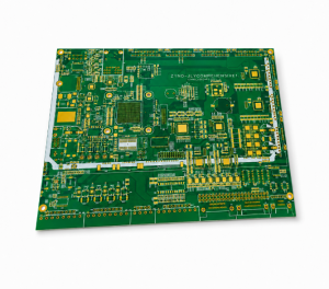
You may also like

Rigid-Flex PCB Materials

June 2nd, 2026


Need reliable Rigid-Flex PCB Materials for compact electronics? Learn material types, stack-up choices, bend reliability, cost factors and supplier selection.

What Are Rigid-Flex PCB Materials?

Rigid-Flex PCB Materials are the combined material systems used to build circuit boards with both rigid sections and flexible bending sections. These materials usually include rigid laminate, flexible polyimide film, copper foil, adhesive or adhesiveless flexible copper-clad laminate, prepreg, coverlay, bonding film and surface finish.

A rigid-flex PCB is not simply a rigid board connected to a flex cable. It is an integrated circuit structure where the flexible layers usually pass through or connect between rigid areas. This design helps reduce connectors, save internal space and improve long-term reliability in compact electronic products.

The material choice directly affects bending life, signal stability, heat resistance, copper adhesion, layer bonding and final assembly yield. If the wrong material is selected, the board may crack, delaminate, lose impedance control or fail during repeated bending.

Rigid-Flex PCB Materials, https://www.bestpcbs.com/blog/2026/06/rigid-flex-pcb-materials/

Why Are Rigid-Flex PCB Materials Important?

Rigid-flex PCB materials are important because they decide whether the board can survive both mechanical movement and electrical operation. A rigid-flex design often appears in devices where space is limited, wiring must bend and long-term reliability is required.

Common applications include medical devices, aerospace electronics, automotive modules, cameras, wearables, industrial sensors and portable electronics. These products often need smaller size, lighter weight and fewer connector points.

Industry guidance commonly refers to IPC-2223 for flexible and rigid-flex board design. IPC-2223 is a sectional design standard for flexible and rigid-flex printed boards, and it is often used together with qualification and performance standards for flex circuits.

For buyers, the material choice affects not only board price but also field reliability. A low-cost material stack-up may look acceptable at the quotation stage, but it can create hidden risks during bending, assembly or long-term thermal cycling.

How Do Rigid-Flex PCB Materials Work?

Rigid-flex PCB materials work by combining stable rigid areas with bendable flexible areas in one continuous circuit structure. The rigid parts support components, solder joints and mechanical assembly. The flexible parts allow folding, bending or connection between product sections.

The flexible section usually uses polyimide film because it offers strong heat resistance, dimensional stability and bending performance. Copper traces are laminated or bonded to the polyimide, then protected by coverlay or flexible solder mask.

The rigid section usually uses FR4, high-Tg FR4, halogen-free laminate, polyimide rigid laminate or high-frequency laminate, depending on electrical, thermal and reliability needs. Prepreg or bonding film connects the rigid and flexible structures during lamination.

What Are the Main Materials Used in Rigid-Flex PCB?

The main rigid-flex PCB materials include polyimide film, copper foil, FR4 laminate, high-Tg laminate, prepreg, adhesive, coverlay, stiffener and surface finish materials. Each material has a different function in the final board.

MaterialFunctionCommon Selection Point
Polyimide FilmFlexible dielectric baseHeat resistance and bending life
Copper FoilConductive circuit layerRolled annealed or electrodeposited copper
FR4 LaminateRigid area supportCost, Tg, mechanical strength
High-Tg FR4Rigid area for thermal stressBetter heat resistance
Polyimide LaminateHigh-reliability rigid sectionAerospace and harsh environments
PrepregLayer bonding in rigid areaLamination compatibility
AdhesiveBonds copper and dielectricFlexibility and delamination risk
CoverlayProtects flex copper tracesBend durability and insulation
Flexible Solder MaskFine pattern protectionDetailed geometry
StiffenerReinforces connector or assembly areaPI, FR4 or stainless steel

The best material system should be selected based on bend type, assembly method, thermal condition, electrical requirement and product lifetime.

What Flexible Core Materials Are Used in Rigid-Flex PCB?

The most common flexible core material is polyimide, often called PI. Polyimide is widely used because it can tolerate high soldering temperatures, repeated bending and harsh operating environments.

Flexible copper-clad laminate can be adhesive-based or adhesiveless. Adhesive-based material uses an adhesive layer between copper and polyimide. Adhesiveless material bonds copper directly to the film without a separate adhesive interface.

Adhesiveless construction can reduce total thickness and remove one interface where fatigue or delamination may start. This makes it useful for thin, high-reliability or dynamic-flex designs.

For most rigid-flex projects, the flexible material must be chosen early because it affects bend radius, copper fatigue, stack-up thickness and final reliability testing.

What Rigid Materials Are Used in Rigid-Flex PCB?

The rigid area of a rigid-flex PCB usually uses FR4, high-Tg FR4, halogen-free FR4, polyimide laminate or high-frequency laminate. The choice depends on cost, temperature, signal speed and mechanical requirements.

Standard FR4 is suitable for many commercial products where cost control is important. High-Tg FR4 is better for products that face higher soldering temperature, thermal cycling or long-term heat exposure.

Polyimide rigid laminate is often used in aerospace, defense, medical and high-reliability products. It costs more than FR4 but offers stronger thermal stability and better reliability under demanding conditions.

For RF or high-speed designs, engineers may choose special low-loss laminates in the rigid section. In this case, material matching between rigid and flexible areas becomes more important because impedance and dimensional stability must be controlled.

What Is Coverlay in Rigid-Flex PCB Materials?

Coverlay is a protective layer used over flexible copper traces. It is usually made from polyimide film with adhesive, and it protects the circuit from moisture, abrasion, handling damage and electrical shorting.

Coverlay is different from standard rigid PCB solder mask. It is more flexible and better suited for bending areas. Common coverlay structures may use 12.5–50 μm polyimide film with 12.5–25 μm adhesive, depending on design needs.

Coverlay is usually preferred in high-flex or harsh-use areas. Flexible solder mask may be used when the design needs finer openings or more detailed geometry, but it may not provide the same mechanical protection in repeated bending areas.

What Copper Foil Is Best for Rigid-Flex PCB Materials?

Copper foil is one of the most important rigid-flex PCB materials because it carries current and also survives bending stress. The two common choices are rolled annealed copper and electrodeposited copper.

Rolled annealed copper is often preferred for dynamic bending because its grain structure supports better flex life. Electrodeposited copper is widely used in standard PCB production and can be suitable for static bending or bend-to-install applications.

For high-reliability flexible sections, copper thickness should not be selected only by current capacity. Thicker copper can carry more current, but it also increases bending stress. Engineers must balance current load, bend radius, flex cycle requirement and trace width.

What Is the Difference Between Adhesive and Adhesiveless Rigid-Flex Materials?

Adhesive rigid-flex materials use an adhesive layer to bond copper to polyimide. This structure is common, cost-effective and widely available. It is suitable for many static-flex and commercial rigid-flex products.

Adhesiveless rigid-flex materials do not use a separate adhesive layer between copper and polyimide. This creates a thinner structure and may improve bending reliability because there is one less interface that can fail.

Material TypeMain AdvantageMain LimitationBest Use
Adhesive-Based Flex MaterialLower cost and wide availabilityThicker structure, more delamination riskStatic flex, general electronics
Adhesiveless Flex MaterialThinner, better reliability, improved bend lifeHigher costDynamic flex, compact and high-reliability designs

If the product only bends during assembly, adhesive-based material may be enough. If the product bends repeatedly during use, adhesiveless material is often a better choice.
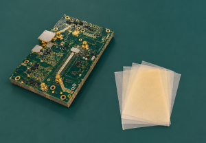
Adhesive and Adhesiveless Rigid-Flex Materials, https://www.bestpcbs.com/blog/2026/06/rigid-flex-pcb-materials/

How Should Rigid-Flex PCB Materials Be Selected for Bend Reliability?

Rigid-flex PCB materials should be selected according to whether the bend is static, dynamic or bend-to-install. Static bending means the board is bent once or rarely moved. Dynamic bending means the board bends repeatedly during product use.

For dynamic bending, engineers should prioritize thin polyimide, rolled annealed copper, adhesiveless construction, proper coverlay and controlled copper layout. The flex area should avoid sharp corners, plated holes, sudden width changes and unnecessary copper density.

For better bend reliability, flex layers are often kept to one or two layers when possible. This helps reduce material thickness, lower bending stress and improve mechanical flexibility.

Material selection and layout must work together. Even excellent material can fail if the bend radius is too small, copper traces cross the bend incorrectly or the transition area is poorly designed.

Rigid-Flex PCB Materials, https://www.bestpcbs.com/blog/2026/06/rigid-flex-pcb-materials/

How Do Rigid-Flex PCB Materials Affect Signal Integrity?

Rigid-flex PCB materials affect signal integrity through dielectric constant, dielectric thickness, copper roughness, trace geometry and layer transition design. For high-speed signals, uncontrolled material changes between rigid and flex areas can create impedance mismatch.

Polyimide usually has different electrical properties from FR4 or high-frequency rigid laminates. This means the stack-up must be reviewed carefully when controlled impedance is required.

For RF, antenna, camera module, high-speed data or medical signal applications, engineers should confirm Dk, Df, copper type, trace width, spacing, reference plane continuity and bend area routing. Material datasheets alone are not enough; the actual stack-up must be calculated and verified.

What Are Common Rigid-Flex PCB Material Failures?

Common material-related failures include copper cracking, coverlay separation, delamination, resin recession, rigid-flex transition cracking, solder joint fatigue, insulation failure and impedance drift. Many of these failures start from poor material matching or weak stack-up design.

Copper cracking often happens when copper is too thick, bend radius is too tight or trace direction is poorly arranged. Delamination may occur when adhesive systems, lamination settings or thermal cycling conditions are not properly controlled.

The rigid-flex transition area is especially important. This area connects a stiff rigid structure to a flexible structure, so stress can concentrate there. Material thickness, coverlay extension, copper layout and mechanical support must be designed carefully.

What Standards Apply to Rigid-Flex PCB Materials?

The most commonly referenced design standard is IPC-2223, which covers flexible and rigid-flex printed board design. Manufacturers and engineers may also refer to related IPC performance and qualification standards for flexible printed circuits.

IPC-related rigid-flex guidance is important because it helps define material use, stack-up design, bend reliability, coverlay rules and testing expectations. These standards help reduce design ambiguity between customers, PCB engineers and manufacturers.

For commercial projects, buyers may also request RoHS, REACH, UL, ISO quality management, halogen-free material or automotive reliability documentation depending on the final market.

Where Are Rigid-Flex PCB Materials Used?

Rigid-flex PCB materials are used in electronic products that require compact assembly, folding structure, lightweight design and reliable interconnection. Common industries include medical electronics, aerospace, automotive, industrial control, robotics, consumer electronics, wearables and communication devices.

Typical applications include camera modules, surgical tools, hearing aids, wearable sensors, automotive control modules, UAV electronics, display modules, foldable devices, test equipment and compact power systems.

Rigid-flex boards are especially useful when connectors and wire harnesses create space, weight or reliability problems. By replacing separate cables and connectors, rigid-flex PCB materials can help simplify assembly and reduce failure points.

Rigid-Flex PCB Materials Application, https://www.bestpcbs.com/blog/2026/06/rigid-flex-pcb-materials/

How Do Rigid-Flex PCB Materials Affect Cost?

Rigid-flex PCB materials affect cost through material grade, layer count, flex layer number, copper thickness, coverlay type, adhesive type, rigid laminate type, controlled impedance needs and testing requirements.

Adhesiveless materials, high-Tg laminates, polyimide rigid laminates, low-loss materials and dynamic-flex structures usually cost more. However, they may reduce connector cost, assembly labor, field failure and product size.

Cost should be evaluated at the product level. A rigid-flex PCB may have a higher board price than a separate rigid PCB and flex cable, but it can reduce assembly steps, connector quantity, internal space and long-term reliability risk.

How Can Buyers Choose a Rigid-Flex PCB Materials Supplier?

Buyers should choose a supplier that understands both rigid PCB manufacturing and flexible circuit behavior. Rigid-flex production requires control of lamination, coverlay alignment, bend area stress, copper adhesion and dimensional stability.

A good supplier should provide material stack-up review, DFM feedback, impedance support, prototype validation, quality inspection and mass production control. The supplier should also help confirm bend radius, copper type, coverlay design and rigid-flex transition structure before production.

For OEM and ODM projects, buyers should not only compare price. They should ask whether the factory has experience with similar products, similar layer counts and similar reliability requirements.
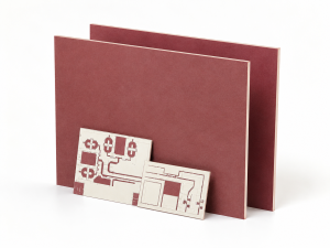
What Should You Confirm Before Ordering Rigid-Flex PCB Materials?

Before ordering rigid-flex PCB materials, confirm the rigid laminate, flexible core material, copper type, copper thickness, adhesive or adhesiveless structure, coverlay thickness, stack-up, bend radius and surface finish.

You should also confirm whether the board is static-flex or dynamic-flex. This single detail can change the material recommendation, copper choice and bend design rules.

For production preparation, provide Gerber files, stack-up requirements, assembly drawing, bend direction, bend radius, component height limits, impedance needs and final application environment. This helps the manufacturer identify risks before tooling and lamination.

FAQs About Rigid-Flex PCB Materials

Q1: What are the most common Rigid-Flex PCB Materials?
A1: The most common Rigid-Flex PCB Materials include polyimide film, copper foil, FR4 laminate, high-Tg FR4, prepreg, adhesive, coverlay, flexible solder mask and stiffener materials. Polyimide is used in the flexible area, while FR4 or high-Tg laminate is often used in the rigid area.

Q2: Why is polyimide used in rigid-flex PCB materials?
A2: Polyimide is used because it provides strong heat resistance, flexibility and dimensional stability. It can survive soldering temperature and repeated bending better than many organic materials. This makes it suitable for flexible sections in medical devices, automotive modules, aerospace products and compact electronics.

Q3: Is adhesiveless material better for rigid-flex PCB?
A3: Adhesiveless material is often better for thin, high-reliability or dynamic-flex designs because it removes one adhesive interface and can improve bending performance. However, it costs more than adhesive-based material. For static flex or bend-to-install products, adhesive-based materials may still be practical and cost-effective.
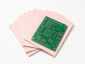
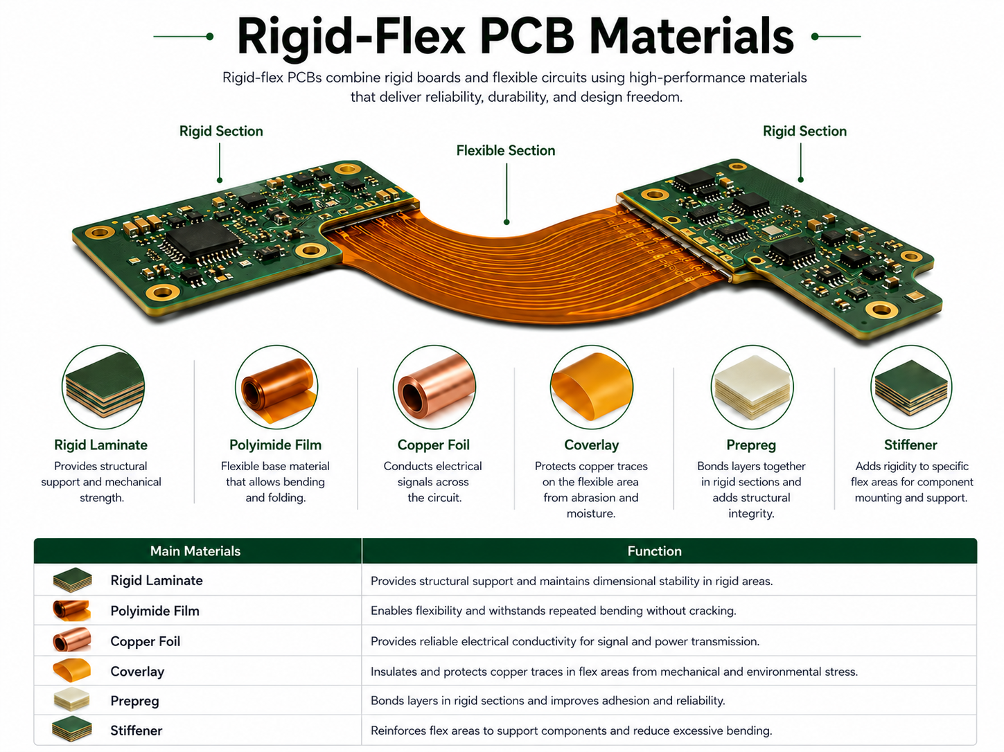
Q4: What copper is best for flexible areas?
A4: Rolled annealed copper is usually preferred for flexible areas that need repeated bending because it has better fatigue resistance. Electrodeposited copper can be suitable for static bend or standard applications. The best choice depends on flex cycle requirement, copper thickness, bend radius and current load.

Q5: What is coverlay in rigid-flex PCB materials?
A5: Coverlay is a protective polyimide-based layer used over copper traces in the flexible area. Common coverlay materials may use 12.5–50 μm polyimide film and 12.5–25 μm adhesive. It protects the circuit from abrasion, moisture and electrical shorting, especially in bend areas.

Q6: Can rigid-flex PCB materials support controlled impedance?
A6: Yes, rigid-flex PCB materials can support controlled impedance, but the stack-up must be carefully designed. Engineers should control Dk, Df, trace width, dielectric thickness, copper roughness and reference plane continuity. This is especially important for RF, camera, antenna and high-speed data applications.

Q7: What causes rigid-flex PCB material failure?
A7: Common causes include tight bend radius, thick copper in bend areas, poor coverlay design, weak lamination, incorrect adhesive selection and stress concentration at the rigid-flex transition. Failures may appear as copper cracking, delamination, coverlay lifting, insulation problems or solder joint fatigue.

Q8: Are rigid-flex PCB materials expensive?
A8: Rigid-flex PCB materials are usually more expensive than standard rigid PCB materials because they combine rigid and flexible structures. Cost increases with layer count, flex layer number, adhesiveless material, controlled impedance and reliability testing. However, they can reduce connectors, labor and field failure risk.

Q9: What standards are used for rigid-flex PCB design?
A9: IPC-2223 is commonly referenced for flexible and rigid-flex printed board design. Depending on the product, buyers may also request IPC performance standards, RoHS, REACH, UL, ISO quality control or automotive reliability documentation. Standards help improve design consistency and production quality.

Q10: How do I choose materials for dynamic-flex applications?
A10: For dynamic-flex applications, choose thin polyimide, rolled annealed copper, suitable coverlay and preferably adhesiveless flexible copper-clad laminate. Keep the flex layer count low, often one or two layers when possible, avoid vias in bend areas and maintain a proper bend radius.

Q11: Can FR4 be used in rigid-flex PCB materials?
A11: Yes, FR4 is commonly used in the rigid sections of rigid-flex PCBs. For higher temperature or reliability needs, high-Tg FR4 or polyimide laminate may be selected. The flexible section usually uses polyimide, so the full stack-up must be reviewed for lamination compatibility and reliability.

Q12: What should buyers ask before ordering rigid-flex PCB materials?
A12: Buyers should ask about stack-up, flexible core material, copper type, coverlay thickness, bend radius, adhesive or adhesiveless construction, surface finish and testing plan. They should also confirm whether the supplier has experience with similar rigid-flex structures and can provide DFM support before production.

Conclusion

Rigid-Flex PCB Materials should be selected by matching the product’s mechanical movement, thermal condition, electrical requirement and assembly structure. Polyimide, copper foil, coverlay, adhesive system, rigid laminate and prepreg all affect the final reliability of the board.

For stable projects, focus on bend type, copper selection, stack-up balance, coverlay design, rigid-flex transition control and supplier capability. For procurement, the best choice is not always the lowest quote, but the material system that can support prototype validation, mass production and long-term product reliability.

You may also like

Ceramic PCB Materials

June 2nd, 2026

What are ceramic PCB materials and how do they affect heat, insulation and reliability? Learn Al2O3, AlN, BeO, Si3N4 selection, applications and buying tips.

What Are Ceramic PCB Materials?

Ceramic PCB materials are inorganic ceramic substrates used as the base of printed circuit boards instead of traditional organic materials such as FR4. They are selected when a circuit must handle high heat, high voltage, high frequency, or harsh operating environments.

Common ceramic PCB materials include alumina (Al2O3), aluminum nitride (AlN), beryllium oxide (BeO), silicon nitride (Si3N4), and sometimes silicon carbide (SiC). These materials provide strong electrical insulation while allowing heat to move away from power devices, LEDs, RF modules, and semiconductor components.

Unlike FR4, ceramic substrates do not mainly rely on glass fiber and epoxy resin. Their performance comes from the ceramic body itself, which offers better thermal conductivity, lower thermal expansion, stronger dimensional stability, and better resistance to high-temperature operation.

For engineers and buyers, the key point is simple: ceramic PCB material is not chosen only by price. It must match heat load, circuit voltage, mechanical stress, copper thickness, assembly process, and long-term reliability requirements.

Ceramic PCB Materials, https://www.bestpcbs.com/blog/2026/06/ceramic-pcb-materials/

Why Are Ceramic PCB Materials Important?

Ceramic PCB materials are important because modern electronic products generate more heat in smaller spaces. Power modules, high-brightness LEDs, EV electronics, RF amplifiers, laser devices, and semiconductor packages all need stable heat dissipation.

FR4 is suitable for many standard electronics, but its thermal conductivity is much lower than ceramic materials. Ceramic substrates can conduct heat far more effectively while still maintaining electrical insulation, which makes them valuable in circuits where heat cannot be allowed to accumulate around chips or solder joints.

Material choice also affects reliability. If the coefficient of thermal expansion does not match the component or copper layer, repeated heating and cooling may cause cracks, delamination, solder fatigue, or broken traces. In high-power products, this is often more serious than the initial material cost.

For procurement teams, ceramic PCB materials directly influence cost, lead time, processing difficulty, and supplier capability. A low-cost ceramic material may be enough for LED lighting, while an EV power module or high-frequency device may require AlN or another advanced ceramic substrate.

How Do Ceramic PCB Materials Work?

Ceramic PCB materials work by combining electrical insulation with thermal conduction. Most metals conduct heat well but also conduct electricity. Ceramics are different because they can transfer heat while resisting electrical current, allowing circuits to stay electrically isolated.

When a chip, LED, MOSFET, IGBT, or RF component generates heat, the ceramic substrate spreads that heat away from the component area. The heat can then move into copper layers, metal bases, housings, heat sinks, or cooling systems. This reduces hot spots and helps the device maintain stable performance.

The material structure also supports dimensional stability. Ceramic substrates usually have lower expansion than many organic PCB materials. This helps reduce mechanical stress in applications where devices repeatedly heat up and cool down.

In practical manufacturing, ceramic PCB performance depends not only on the ceramic base. It also depends on metallization, copper bonding, surface finish, drilling quality, laser processing, conductor adhesion, and assembly control.

What Are the Main Types of Ceramic PCB Materials?

The main ceramic PCB materials include Al2O3, AlN, BeO, Si3N4, and SiC. Each material has a different balance of heat dissipation, insulation, strength, safety, cost, and manufacturability.

Ceramic PCB MaterialMain StrengthTypical UseSelection Note
Alumina (Al2O3)Cost-effective, stable, widely availableLEDs, sensors, power circuits, industrial electronicsGood general-purpose ceramic PCB material
Aluminum Nitride (AlN)High thermal conductivity, good insulationPower modules, semiconductor devices, RF, high-power LEDsBetter for demanding thermal management
Beryllium Oxide (BeO)Very high thermal conductivitySpecial high-power and RF applicationsRestricted by toxicity concerns during processing
Silicon Nitride (Si3N4)Strong mechanical toughness, thermal shock resistanceAutomotive, power modules, harsh environmentsUseful where mechanical reliability matters
Silicon Carbide (SiC)High-temperature capability, strong hardnessExtreme environment electronicsLess common for standard ceramic PCBs
Ceramic PCB Materials Types, https://www.bestpcbs.com/blog/2026/06/ceramic-pcb-materials/

Alumina and aluminum nitride are the most common choices in many commercial ceramic PCB projects. Alumina is often selected when cost and stability matter most. Aluminum nitride is selected when high heat dissipation is the main requirement.

BeO can offer excellent thermal performance, but it requires strict safety control because of toxicity risk during machining. Many projects now prefer AlN as a safer alternative when high thermal conductivity and electrical insulation are needed.

What Is Alumina Ceramic PCB Material?

Alumina ceramic PCB material, also called Al2O3 ceramic substrate, is one of the most widely used ceramic PCB materials. It offers good electrical insulation, stable mechanical performance, high-temperature resistance, and lower cost compared with many advanced ceramic substrates.

Common alumina purity levels include 96% alumina and 99.6% alumina. A 96% alumina substrate is often used for cost-sensitive ceramic PCB applications, while 99.6% alumina may be selected when better surface quality, insulation, or stability is required.

Alumina thermal conductivity is lower than AlN but still much higher than standard FR4. Many alumina ceramic substrates are commonly used in the 24–30 W/m·K thermal conductivity range, depending on purity, formulation, and processing.

Alumina ceramic PCBs are commonly used in LED modules, sensors, automotive electronics, industrial controllers, thick-film circuits, power resistors, and compact electronic modules. For many buyers, alumina is the best balance between performance, price, and production availability.

What Is Aluminum Nitride Ceramic PCB Material?

Aluminum nitride ceramic PCB material, also called AlN ceramic substrate, is selected for high thermal conductivity and electrical insulation. It is widely used in high-power electronics, semiconductor packaging, laser modules, RF devices, EV power systems, and high-brightness LED applications.

AlN is valuable because its thermal conductivity is much higher than alumina. Many commercial AlN ceramic substrates are commonly listed around 150–220 W/m·K, while actual values depend on material grade and processing quality.

Another advantage is its thermal expansion behavior. AlN has a coefficient of thermal expansion closer to silicon than many other materials, which can help reduce thermal mismatch in semiconductor-related assemblies.

The main limitation is cost. AlN is usually more expensive than alumina and may require more careful process control. However, when thermal failure risk is high, the higher material cost can be justified by better reliability and longer product life.

What Is Beryllium Oxide Ceramic PCB Material?

Beryllium oxide, or BeO, is a ceramic material known for very high thermal conductivity and good electrical insulation. It has been used in some RF, microwave, aerospace, and high-power electronic applications where heat dissipation is extremely important.

Some BeO materials can offer very strong thermal performance, which makes them attractive for demanding thermal designs. However, BeO has a major safety concern because toxic dust can be produced during machining or improper processing.

Because of this risk, many companies avoid BeO unless the application truly requires it and the supplier has proper safety systems. For many modern projects, AlN is often considered a safer alternative.

Buyers should confirm safety compliance, handling documentation, machining control, and processing capability before choosing BeO for any ceramic PCB project.

What Is Silicon Nitride Ceramic PCB Material?

Silicon nitride, or Si3N4, is a ceramic material known for high mechanical strength, fracture toughness, and thermal shock resistance. It is valuable in harsh applications where cracking risk is a major concern.

Si3N4 is often considered when the circuit must survive mechanical stress, vibration, impact, or rapid temperature cycling. This makes it attractive for automotive power modules, industrial systems, transportation electronics, and high-reliability environments.

Compared with AlN, silicon nitride may not always provide the same level of thermal conductivity. Its advantage is mechanical robustness rather than only heat dissipation.

The practical choice depends on the full design. If the biggest risk is heat, AlN may be better. If the biggest risk is mechanical stress and thermal cycling, Si3N4 may deserve serious evaluation.

How Do Alumina, AlN, BeO and Si3N4 Compare?

Different ceramic PCB materials should be compared by application needs, not by a single performance number. Thermal conductivity is important, but it is not the only selection factor.

ItemAlumina Al2O3Aluminum Nitride AlNBeryllium Oxide BeOSilicon Nitride Si3N4
Thermal conductivityMediumHighVery highMedium to high
Electrical insulationHighHighHighHigh
Mechanical toughnessMediumMediumMediumHigh
Thermal shock resistanceGoodGoodGoodExcellent
Cost levelLowerHigherHigherHigher
Processing safetyGoodGoodSpecial control neededGood
Common availabilityVery highHighLimitedMedium
Best fitGeneral ceramic PCBHigh-power thermal designSpecial high-thermal projectsHarsh mechanical environments

For most commercial projects, alumina is the practical starting point and AlN is the upgrade path for higher thermal demand. BeO is a special-case material, while Si3N4 is often chosen for strength and thermal cycling resistance.

A good supplier should not recommend the most expensive material first. The better approach is to review power density, operating temperature, copper thickness, board size, assembly method, and reliability target before confirming the substrate.

What Properties Should You Check Before Selecting Ceramic PCB Materials?

Before selecting ceramic PCB materials, engineers should check thermal, electrical, mechanical, and manufacturing parameters. These properties determine whether the substrate can survive real operating conditions.

ParameterWhy It MattersTypical Selection Focus
Thermal conductivityControls heat dissipationHigher for power modules, LEDs, RF power devices
Dielectric strengthPrevents electrical breakdownImportant for high-voltage circuits
Dielectric constantAffects signal behaviorImportant for RF and high-frequency designs
Dissipation factorAffects signal lossLower is better for RF and microwave use
Coefficient of thermal expansionControls thermal stressMust match chips, copper, and package materials
Flexural strengthAffects breakage riskImportant for handling and assembly
Surface roughnessAffects metallization and bondingImportant for fine circuits and thin film processes
Copper adhesionAffects reliabilityCritical for DBC, DPC, thick copper, and power cycling
Substrate thicknessAffects strength and thermal pathMust balance insulation, rigidity, and heat transfer
Manufacturing toleranceAffects assembly fitImportant for precision modules

For high-power applications, thermal conductivity and copper adhesion are often the first concerns. For RF applications, dielectric constant, loss tangent, and surface quality become more important.

For procurement, the most common mistake is comparing only unit price. A cheaper substrate can become expensive if it causes cracking, poor yield, solder defects, or field failure after mass production.

What Ceramic PCB Manufacturing Processes Use These Materials?

Ceramic PCB materials can be processed through several manufacturing methods, depending on circuit density, copper thickness, power level, and cost target.

Thick film ceramic PCB uses screen printing and firing to create conductive patterns. It is common for sensors, power resistors, hybrid circuits, and cost-sensitive ceramic electronics.

Thin film ceramic PCB uses deposition and photolithography to create fine, precise circuits. It is suitable for high-frequency, high-precision, and compact electronic modules.

DCB ceramic PCB means direct copper bonded. It bonds copper directly to ceramic substrates and is widely used in power modules because it supports high current and strong heat dissipation.

DPC ceramic PCB means direct plated copper. It uses metallization and electroplating to build copper on ceramic. It is useful for fine circuits, LEDs, sensors, and compact high-performance modules.

LTCC and HTCC are co-fired ceramic technologies used for multilayer ceramic circuits, RF modules, microwave components, and high-reliability electronics.

What Are the Advantages of Ceramic PCB Materials?

Ceramic PCB materials offer several advantages over many traditional PCB substrates. Their biggest value is the combination of heat dissipation and insulation.

Strong thermal management allows heat to move away from chips, LEDs, and power components. This helps reduce hot spots and supports longer component life.

High electrical insulation helps ceramic PCBs support high-voltage and high-power applications without short circuits between conductive paths.

Low thermal expansion improves dimensional stability and reduces stress between chips, copper, solder joints, and the substrate during temperature cycling.

Good chemical and corrosion resistance supports use in industrial, automotive, aerospace, medical, and outdoor-related environments.

High-frequency suitability makes some ceramic materials useful in RF, microwave, antenna, telecommunications, and radar-related applications.

Ceramic PCB Materials, https://www.bestpcbs.com/blog/2026/06/ceramic-pcb-materials/

What Are the Limitations of Ceramic PCB Materials?

Ceramic PCB materials also have limitations. They are not the best choice for every circuit board project.

The first limitation is cost. Ceramic substrates are usually more expensive than FR4, especially when using AlN, Si3N4, DBC, DPC, thin film, or multilayer ceramic processes.

The second limitation is brittleness. Ceramic materials can crack under mechanical stress, improper handling, poor panel design, or fast thermal shock.

The third limitation is manufacturing complexity. Ceramic drilling, laser processing, metallization, copper bonding, and surface finishing require controlled processes. Not every standard PCB factory can produce reliable ceramic PCBs.

The fourth limitation is design flexibility. Ceramic PCBs may have restrictions in board size, hole design, edge clearance, copper thickness, and panel utilization. These constraints should be reviewed before finalizing the design.

Where Are Ceramic PCB Materials Used?

Ceramic PCB materials are used in industries where heat, voltage, frequency, reliability, or harsh conditions are major design concerns.

IndustryCommon ApplicationsMaterial Focus
LED lightingHigh-power LED modules, COB LEDs, UV LEDsAlumina, AlN
Automotive electronicsEV power modules, sensors, battery systemsAlN, Si3N4, alumina
Power electronicsMOSFET, IGBT, rectifier, converter modulesAlN, DBC alumina, Si3N4
RF and microwaveRF amplifiers, antennas, microwave modulesAlumina, AlN, thin film ceramic
Medical devicesImaging systems, laser devices, precision electronicsAlumina, AlN
Aerospace and defenseHigh-reliability modules, radar, harsh environment circuitsAlN, alumina, Si3N4
TelecommunicationsRF modules, base station electronics, optical modulesAlumina, AlN
Industrial equipmentMotor drives, sensors, power control boardsAlumina, AlN

In LED projects, alumina may be enough when heat is moderate and cost control is important. In EV power modules or semiconductor devices, AlN or Si3N4 may be more suitable because thermal and reliability requirements are higher.

What Real Project Cases Show the Value of Ceramic PCB Materials?

Case 1: High-power LED module
A customer using a standard metal-core PCB may face high junction temperature in compact LED modules. By switching to an alumina or AlN ceramic substrate, heat can spread more efficiently from the LED chip area.

Case 2: EV power electronics
Power conversion circuits in EV systems face current load, heat, vibration, and repeated temperature cycling. AlN or Si3N4 ceramic substrates can help reduce thermal stress and improve module reliability.

Case 3: RF module
RF circuits require stable dielectric behavior and controlled signal loss. Alumina thin film ceramic substrates are often used where fine line accuracy and frequency stability matter.

Case 4: Industrial sensor
Industrial sensors often need compact size, stable insulation, and resistance to heat or chemicals. Alumina ceramic PCBs can provide a stable base for thick film circuits, heating elements, or sensing modules.

These cases show why material selection should start from the failure risk. If the risk is heat, choose for thermal conductivity. If the risk is cracking, choose for toughness. If the risk is signal loss, choose for dielectric performance.

What Design Factors Matter for Ceramic PCB Materials?

Designing with ceramic PCB materials requires different thinking from standard FR4 design. Ceramic substrates are strong under compression but can be fragile under bending, impact, or local stress.

Engineers should avoid sharp inside corners, weak narrow sections, and unsupported thin ceramic areas. Board outline, mounting holes, slots, and edge clearance should be designed to reduce stress concentration.

Copper thickness must also match the ceramic material and manufacturing method. Thick copper improves current capacity and heat spreading, but it can create more thermal expansion stress.

For RF circuits, trace geometry, dielectric constant, substrate thickness, surface finish, and conductor roughness must be controlled together. A ceramic material with good thermal performance may not automatically be the best RF material.

Assembly design is also important. Solder profile, component placement, thermal interface material, screw torque, and mechanical support can all affect ceramic PCB reliability after production.

What Manufacturing Issues Should Be Controlled?

Ceramic PCB manufacturing needs strict process control because the material is hard, brittle, and sensitive to stress.

Key manufacturing issues include substrate flatness, edge chipping, laser cutting quality, hole quality, conductor adhesion, copper thickness uniformity, metallization strength, surface finish stability, and dimensional tolerance.

For DBC ceramic PCBs, copper bonding strength is critical because power cycling can stress the copper-ceramic interface. For DPC ceramic PCBs, plating quality and via reliability are important.

For thick film ceramic PCBs, paste quality, screen printing accuracy, firing temperature, conductor resistance, and pattern definition must be controlled. For thin film ceramic PCBs, surface preparation and photolithography accuracy are more important.

Buyers should ask suppliers about process capability, inspection methods, copper peel strength, thermal cycling tests, dielectric tests, and sample validation before moving into mass production.

What Tests Are Needed for Ceramic PCB Materials?

Testing helps confirm whether ceramic PCB materials and manufacturing processes meet project requirements.

Test ItemPurpose
Visual inspectionChecks cracks, chips, stains, scratches, and surface defects
Dimensional inspectionConfirms size, hole position, thickness, and tolerance
Thermal conductivity reviewConfirms material grade and heat dissipation expectation
Dielectric withstand testChecks insulation under high voltage
Insulation resistance testConfirms electrical isolation
Copper adhesion testChecks bonding reliability between copper and ceramic
Thermal cycling testEvaluates stress resistance under temperature changes
Solderability testConfirms surface finish and assembly performance
Cross-section analysisReviews copper, plating, via, and interface quality
Functional testConfirms final circuit performance

For high-power products, thermal cycling and copper adhesion are especially important. For RF products, electrical performance and dimensional accuracy may be more important.

Quality control should not start after mass production. The best approach is to confirm material data, sample testing, process capability, and assembly reliability before volume orders.

What Common Failures Happen with Ceramic PCB Materials?

Common ceramic PCB failures include cracking, copper delamination, solder joint fatigue, insulation breakdown, hot spots, edge chipping, and poor conductor adhesion.

Cracking often happens when mechanical stress is not controlled. Causes may include poor panel design, excessive screw torque, improper handling, fast thermal shock, or unsupported mounting.

Copper delamination can happen when the bonding process is weak or when copper thickness, thermal cycling, and material expansion are not properly matched.

Solder fatigue may occur when ceramic, copper, component package, and solder joints expand at different rates during repeated heating and cooling.

Insulation breakdown may happen if voltage clearance, contamination control, dielectric strength, or surface cleanliness is not properly managed.

Hot spots usually come from poor thermal path design. Even a high-performance ceramic material cannot solve heat problems if component placement, copper area, thermal vias, or heat sink contact are poorly designed.

How Should You Choose the Right Ceramic PCB Material?

The right ceramic PCB material should be selected by matching the material to the project’s main risk.

Choose alumina if the project needs stable insulation, moderate thermal performance, good availability, and lower cost. It is suitable for many LED, sensor, industrial, and general ceramic circuit applications.

Choose AlN if the project has high heat density, power semiconductors, compact LED modules, laser devices, or semiconductor packages. It is better when thermal management is the main concern.

Choose Si3N4 if the project must survive vibration, mechanical stress, and repeated thermal shock. It is useful in automotive and harsh-environment power modules.

Choose BeO only when very high thermal conductivity is required and the supplier can properly manage safety, machining, and compliance risks.

The safest selection method is to provide your supplier with operating temperature, power load, voltage, current, copper thickness, board size, surface finish, assembly process, and reliability test requirements before final material confirmation.

What Affects the Cost of Ceramic PCB Materials?

Ceramic PCB cost is affected by substrate material, purity, thickness, copper thickness, circuit complexity, processing method, surface finish, tolerance, order quantity, and testing requirements.

Alumina is usually more cost-effective than AlN. AlN costs more because of material price and processing requirements, but it may reduce thermal failure risk in demanding applications.

DBC and DPC ceramic PCBs also differ in cost. DBC is often used for high-current and power modules, while DPC can support finer features but may require more processing steps.

Thin film ceramic PCBs are usually more expensive than thick film ceramic PCBs because they require higher precision and more controlled processes.

Testing and quality requirements also affect price. Thermal cycling, dielectric testing, cross-section analysis, and special reliability validation increase cost, but they are often necessary for automotive, medical, aerospace, and high-power applications.

How Can Buyers Evaluate a Ceramic PCB Material Supplier?

Buyers should evaluate a ceramic PCB supplier by material capability, process experience, engineering support, quality control, and mass production stability.

A qualified supplier should clearly explain the difference between alumina, AlN, BeO, Si3N4, DBC, DPC, thick film, and thin film ceramic PCB options. If the supplier only quotes price without reviewing application conditions, the project may face hidden reliability risks.

Important supplier questions include:

  • What ceramic materials can you process?
  • What substrate thickness and copper thickness can you support?
  • Can you provide DBC, DPC, thick film, or thin film options?
  • What are your standard tolerances?
  • How do you inspect cracks, edge chips, and copper adhesion?
  • Can you support prototype and mass production?
  • What reliability tests can you provide?
  • Can you review design risks before production?

For overseas buyers, the supplier should also support clear technical communication, stable lead time, export documentation, RoHS-related compliance, and practical packaging protection for brittle ceramic boards.

What Should You Confirm Before Ordering Ceramic PCB Materials?

Before ordering ceramic PCB materials, confirm both technical and commercial details. This reduces sample failure, quotation misunderstanding, and mass production delay.

Checklist ItemWhat to Confirm
Material typeAlumina, AlN, BeO, Si3N4, or other ceramic
Material gradePurity, thermal conductivity, dielectric properties
Board thicknessMechanical strength and insulation requirement
Copper thicknessCurrent capacity and thermal spreading
Manufacturing processDBC, DPC, thick film, thin film, LTCC, HTCC
Surface finishENIG, silver, nickel, gold, or project-specific finish
ToleranceOutline, holes, copper pattern, flatness
Assembly methodSMT, wire bonding, soldering, sintering, module assembly
TestingElectrical, thermal, adhesion, reliability, visual inspection
Quantity planPrototype, pilot run, mass production
PackagingAnti-crack protection during shipping
DocumentationDrawing, Gerber, stack-up, material data, inspection report
ceramic PCB material, https://www.bestpcbs.com/blog/2026/06/ceramic-pcb-materials/

For new projects, prototype validation is strongly recommended before mass production. Ceramic PCB mistakes are usually more expensive to correct after tooling, metallization, or assembly has already started.

FAQs About Ceramic PCB Materials

Q1: What are the most common ceramic PCB materials?
A1: The most common ceramic PCB materials are alumina and aluminum nitride. Alumina is widely used because it is stable, cost-effective, and available. Aluminum nitride is used when stronger heat dissipation is required. BeO, Si3N4, and SiC are used in more specialized applications.

Q2: Is alumina or aluminum nitride better for ceramic PCBs?
A2: Neither is always better. Alumina is better for cost-sensitive and general ceramic PCB applications. Aluminum nitride is better for high-power, high-heat, and semiconductor-related designs. The right choice depends on thermal load, budget, circuit structure, and reliability targets.

Q3: Why are ceramic PCB materials better than FR4 for heat dissipation?
A3: Ceramic materials conduct heat much better than FR4 while keeping electrical insulation. This helps move heat away from power devices, LEDs, RF components, and semiconductor chips. For high-power circuits, this can reduce hot spots and improve long-term stability.

Q4: What is the thermal conductivity of alumina ceramic PCB material?
A4: Alumina ceramic PCB material is often listed around 24–30 W/m·K, depending on purity and formulation. It is lower than AlN but much higher than standard FR4, making it suitable for LEDs, sensors, industrial electronics, and general thermal applications.

Q5: What is the thermal conductivity of AlN ceramic PCB material?
A5: Commercial AlN ceramic substrates are often listed around 150–220 W/m·K, with values depending on material grade and processing quality. AlN is commonly selected for power electronics, semiconductor modules, laser devices, and high-brightness LED systems.

Q6: Are ceramic PCB materials electrically conductive?
A6: Most ceramic PCB substrates are electrical insulators. Their value comes from conducting heat while resisting electrical current, allowing ceramic PCBs to support high-power circuits safely. This makes them useful for power modules, LEDs, RF devices, and high-voltage electronics.

Q7: Can ceramic PCB materials crack easily?
A7: Ceramic materials can crack if they are exposed to bending, impact, excessive screw pressure, sharp design corners, or fast thermal shock. Good design, proper handling, controlled assembly, and protective packaging can help reduce cracking risk.

Q8: What is DBC ceramic PCB material used for?
A8: DBC ceramic PCB is commonly used in high-current and high-power modules. It bonds copper directly to ceramic substrates, creating strong heat dissipation and current-carrying capability. It is often used in EV electronics, converters, power modules, and industrial control systems.

Q9: What is DPC ceramic PCB material used for?
A9: DPC ceramic PCB is useful when finer circuits, good thermal performance, and compact design are needed. It is often used in LED modules, sensors, power devices, and precision electronic products where circuit accuracy and thermal control are both important.

Q10: Are ceramic PCB materials suitable for RF applications?
A10: Yes, some ceramic PCB materials are suitable for RF and microwave applications. For RF design, engineers must check dielectric constant, loss, surface quality, and conductor accuracy. Alumina and AlN are common choices for many high-frequency ceramic circuit designs.

Q11: Why is AlN often used in power electronics?
A11: AlN is used in power electronics because it provides high thermal conductivity and good electrical insulation. It helps move heat away from power chips and reduces thermal stress when matched with suitable copper thickness, package structure, and assembly process.

Q12: Is BeO still used in ceramic PCBs?
A12: BeO is still used in some special high-thermal applications, but it requires strict safety control. Many companies prefer AlN when they need strong thermal performance with fewer safety concerns. Buyers should confirm safety documentation before choosing BeO.

Q13: How do I choose ceramic PCB material for LED applications?
A13: For standard LED applications, alumina may be enough. For high-power LEDs, UV LEDs, COB modules, or compact lighting systems with higher heat density, AlN may be a better choice. The final selection should match power, heat, size, and cost requirements.

Q14: What files are needed for a ceramic PCB quotation?
A14: A supplier usually needs Gerber files, drawings, material requirements, board thickness, copper thickness, surface finish, quantity, tolerance, assembly requirements, and testing needs. If the material is uncertain, provide operating temperature, voltage, current, and application details.

Q15: Can ceramic PCBs be customized for OEM or ODM projects?
A15: Yes, ceramic PCBs can be customized for OEM and ODM projects. Custom options may include substrate material, thickness, copper thickness, surface finish, outline, hole structure, metallization method, testing standard, and packaging method. This helps match the board to real product requirements.

Summary

Ceramic PCB materials are selected when a circuit needs better heat dissipation, electrical insulation, high-temperature stability, and long-term reliability than standard organic PCB materials can provide. Alumina is often the practical choice for cost-effective ceramic PCB projects, while aluminum nitride is preferred for high-power and high-thermal applications. BeO, Si3N4, and SiC are more specialized materials for demanding environments.

For material selection, engineers should not compare only thermal conductivity or price. The better decision comes from reviewing power density, voltage, copper thickness, thermal cycling, mechanical stress, manufacturing process, assembly method, and reliability testing. Buyers should also confirm supplier experience with ceramic processing, copper adhesion, crack control, inspection, packaging, and mass production support.

You may also like

High-Tg PCB Materials

June 2nd, 2026

High-Tg PCB materials are used when a printed circuit board must remain dimensionally stable under heat, soldering stress, continuous operation, or demanding environmental conditions. In many PCB projects, standard FR4 is sufficient. However, when the board faces lead-free reflow, high layer count, power density, automotive temperature cycling, or long-term reliability requirements, high-Tg PCB materials become a safer engineering choice.

High-Tg PCB materials

For engineers, Tg is not just a number on a laminate datasheet. It affects expansion behavior, via reliability, delamination resistance, impedance stability, soldering performance, and production yield. For buyers, the key is to match the Tg grade with the real application instead of overpaying for unnecessary specifications or choosing a laminate that cannot support the product’s operating environment.

What Are High-Tg PCB Materials?

High-Tg PCB materials are PCB laminates with a higher glass transition temperature than standard FR4 materials. Tg means “glass transition temperature.” It refers to the temperature range where the resin system changes from a rigid glass-like state to a softer rubber-like state.

In PCB manufacturing, Tg is important because the board does not immediately fail when it reaches this temperature range. Instead, its mechanical behavior changes. Above Tg, the laminate expands faster, especially in the Z-axis direction. This can stress plated through holes, vias, copper barrels, inner-layer connections, and solder joints.

Standard FR4 material often has a Tg of around 130–140°C. High-Tg FR4 usually refers to materials with a Tg of around 170°C or higher. Some advanced laminate systems may reach 180°C, 200°C, or above, depending on resin chemistry and application requirements.

In simple terms, high-Tg PCB materials are base materials designed to maintain better mechanical and thermal stability when exposed to higher processing or operating temperatures.

Why Are High-Tg PCB Materials Important?

High-Tg PCB materials are important because modern PCB assemblies often experience more heat than older electronic products. Lead-free soldering requires higher reflow temperatures. Compact electronic designs place more components into smaller spaces. Power devices, LEDs, motor drivers, battery systems, and RF modules all create localized thermal stress.

When a PCB material has an insufficient Tg rating, the board may show warpage, delamination, pad lifting, barrel cracking, or degraded electrical performance after soldering or long-term use. These issues are especially costly in automotive electronics, industrial control, medical devices, aerospace modules, energy systems, and communication equipment.

High-Tg materials help improve:

Performance AreaWhy It Matters
Thermal StabilityReduces deformation during reflow and operation
Via ReliabilityHelps protect plated through holes under thermal cycling
Dimensional ControlSupports tighter registration in multilayer boards
Delamination ResistanceImproves laminate integrity during heat exposure
Long-Term DurabilitySupports products used in harsh or high-duty environments
Assembly YieldReduces process risk during lead-free soldering

For high-reliability PCBs, Tg is usually reviewed together with decomposition temperature, CTE, copper thickness, layer count, board thickness, soldering profile, and operating temperature.

How Do High-Tg PCB Materials Work Under Heat?

High-Tg PCB materials work by using resin systems that remain mechanically stable at higher temperatures. The resin, glass fiber, copper foil, and curing system must work together to resist expansion, softening, moisture stress, and thermal fatigue.

Before the laminate reaches Tg, the board stays relatively rigid. Once the temperature passes Tg, the resin becomes more flexible and its expansion rate increases. This expansion is especially important in the Z-axis direction because vias and plated through holes pass vertically through the board.

If Z-axis expansion becomes excessive, copper barrels can stretch. Repeated heating and cooling may create micro-cracks. In multilayer boards, inner-layer connections may also become vulnerable if material selection, drilling, plating, and lamination are not well controlled.

High-Tg materials help reduce this risk by keeping the resin system more stable at elevated temperatures. They do not make the PCB immune to heat, but they provide a wider process and reliability margin.

Tg is not the same as maximum operating temperature. It is one important thermal property used to evaluate how a PCB laminate behaves under heat.

Common Types of High-Tg PCB Materials

High-Tg PCB materials are available in different material families. The right choice depends on electrical performance, thermal load, mechanical requirements, cost target, and application environment.

Material TypeTypical Tg RangeCommon Use
High-Tg FR4170–180°CIndustrial, automotive, medical, and multilayer PCBs
Halogen-Free High-Tg FR4170–180°CProducts requiring environmental compliance
High-Performance FR4180°C+Dense multilayer, lead-free assembly, and high-reliability electronics
Polyimide250°C+ depending on gradeAerospace, high-temperature, flex, and rigid-flex designs
Rogers / High-Frequency LaminateVaries by materialRF, microwave, antenna, radar, and communication modules
Metal-Core PCB MaterialDepends on dielectric systemLED lighting, power electronics, and thermal management
Ceramic PCB MaterialVery high thermal stabilityPower modules, high-power LED, laser, sensor, and RF applications

For most rigid PCB projects, high-Tg FR4 is the practical first choice. It offers better thermal endurance than standard FR4 while keeping fabrication cost and process compatibility under control.

For extreme temperature, RF performance, or high thermal conductivity, engineers may need polyimide, Rogers, metal-core, or ceramic substrates instead of high-Tg FR4.

High-Tg FR4 vs Standard FR4 vs Advanced PCB Materials

Not every product needs high-Tg material. Standard FR4 remains suitable for many consumer, low-power, and moderate-temperature applications. The decision should be based on actual design risk, not only on the desire to use a “better” material.

MaterialMain StrengthLimitationBest Fit
Standard FR4Cost-effective and widely availableLower thermal marginGeneral electronics
High-Tg FR4Better thermal stability and assembly reliabilityHigher cost than standard FR4Multilayer, automotive, industrial, and medical PCBs
PolyimideExcellent high-temperature resistanceMore expensive and process-sensitiveAerospace, high-temperature, flex, and rigid-flex designs
Rogers LaminateStable dielectric performanceHigher material and process costRF, antenna, and microwave circuits
Aluminum PCBGood heat spreadingLimited routing structureLED and power modules
Ceramic PCBHigh thermal conductivity and stabilityHigher cost and specialized processingHigh-power, high-frequency, and high-reliability modules

A common engineering mistake is selecting high-Tg FR4 when the real issue is heat dissipation. Tg improves thermal stability, but it does not replace thermal design. If the circuit generates significant heat, copper weight, thermal vias, copper planes, metal-core materials, or ceramic substrates may also be required.

Key Properties Engineers Should Check

Tg is important, but it should not be checked alone. A laminate with a high Tg value can still perform poorly if other thermal or electrical properties do not match the design.

Glass Transition Temperature

Tg indicates when the resin system begins to change mechanical behavior. A higher Tg gives the board a wider thermal process margin, especially for lead-free soldering and high-temperature operation.

CTE

CTE means coefficient of thermal expansion. Z-axis CTE is critical because plated holes and vias are exposed to vertical expansion stress. Lower and more stable CTE helps improve via reliability.

Td

Td means decomposition temperature. It indicates when the resin begins to chemically degrade. A material with good Tg but low Td may still be risky during multiple reflow cycles or harsh processing.

T288

T288 measures how long a laminate can withstand 288°C before delamination under test conditions. It is useful for evaluating resistance to lead-free assembly temperatures.

CAF Resistance

CAF means conductive anodic filament. It is an electrochemical failure path that can occur inside the laminate under voltage, humidity, and contamination. CAF resistance matters for dense designs, fine spacing, and high-reliability electronics.

Dielectric Constant and Loss Tangent

For impedance-controlled, RF, and high-speed circuits, Dk and Df stability must be reviewed. High Tg alone does not guarantee signal integrity.

Moisture Absorption

Moisture trapped inside the laminate can expand during soldering and increase the risk of delamination or blistering. Low moisture absorption supports better assembly reliability.

When Should You Use High-Tg PCB Materials?

High-Tg PCB materials are recommended when the PCB will face higher thermal stress during production, operation, or field use. They are also suitable when product reliability is more important than the lowest possible board cost.

You should consider high-Tg material when the PCB has:

Project ConditionWhy High-Tg Material Helps
Lead-Free ReflowHigher peak temperature increases laminate stress
Multilayer StackupMore lamination pressure and thermal expansion risk
Thick Board DesignHigher Z-axis stress around plated holes
High Copper WeightMore thermal mass and process stress
Fine-Pitch ComponentsBetter dimensional stability supports assembly accuracy
Automotive Temperature CyclingImproves long-term mechanical reliability
Power ElectronicsSupports higher thermal exposure around power areas
Industrial EquipmentImproves durability under continuous operation
Medical ElectronicsSupports stable production and documentation control
Aerospace or UAV ElectronicsHelps withstand demanding reliability conditions

High-Tg material is especially valuable when a PCB must pass repeated thermal cycles, multiple soldering processes, rework exposure, or long operating life requirements.

Where Are High-Tg PCB Materials Used?

Where Are High-Tg PCB Materials Used?

High-Tg PCB materials are widely used in industries where heat, reliability, traceability, and stable production matter.

Automotive Electronics

Automotive boards often face temperature cycling, vibration, high current, and long service life requirements. High-Tg FR4 is commonly used in control modules, lighting systems, battery management, sensors, radar support boards, and power control circuits.

Industrial Control

Industrial PCBs may operate continuously in cabinets, motor systems, power supplies, PLC modules, and automation equipment. High-Tg materials help maintain stable performance in warmer operating environments.

Medical Electronics

Medical PCB projects often require controlled quality, reliable soldering, traceability, and consistent production documentation. High-Tg material can support stable assembly for diagnostic equipment, monitoring modules, and medical control systems.

Communication and RF Support Systems

Not all communication boards require RF laminates throughout the entire design. Some products use high-Tg FR4 for digital, power, or control sections while reserving special materials for RF layers or antenna areas.

LED and Power Electronics

High-power LED and power boards generate localized heat. High-Tg FR4 can help in moderate thermal designs, while aluminum, copper substrate, or ceramic PCB may be selected when heat dissipation becomes the primary requirement.

Aerospace and UAV Electronics

For UAVs, avionics support modules, and high-reliability control circuits, high-Tg materials support improved thermal cycling resistance and dimensional stability during fabrication.

Design Considerations for High-Tg PCB Materials

Good material selection must be supported by good PCB design. A high-Tg laminate cannot compensate for weak stackup planning, poor copper balance, insufficient thermal paths, or unsuitable via structure.

Design Considerations for High-Tg PCB Materials

Control the Stackup Early

Material type, copper thickness, prepreg selection, dielectric thickness, impedance requirement, and lamination cycle should be reviewed before layout is finalized. Late changes can affect impedance, board thickness, delivery time, and cost.

Balance Copper Distribution

Uneven copper distribution can cause bow and twist during lamination and reflow. For multilayer boards, copper balance between layers helps improve dimensional stability and manufacturing yield.

Review Via Structure

High aspect-ratio vias need careful drilling, desmear, plating, and thermal reliability control. For high-reliability boards, via size, annular ring, plating thickness, and thermal cycling requirements should be reviewed together.

Plan Heat Dissipation

High-Tg material improves heat resistance, but heat still needs a path to leave the board. Copper pours, thermal vias, heat sinks, metal substrates, and component placement must be considered.

Check the Soldering Profile

Multiple reflow cycles, selective soldering, wave soldering, or rework can increase material stress. The material should match the actual assembly process, not only the final product environment.

Manufacturing Challenges and Factory Control Points

High-Tg PCB materials require controlled fabrication because material stiffness, resin behavior, drilling response, and lamination conditions may differ from standard FR4.

Lamination Control

High-Tg laminates may need specific lamination temperature, pressure, and cure control. Incorrect lamination can lead to voids, weak bonding, thickness deviation, or delamination risk.

Drilling Quality

The drilling process affects hole wall quality and later plating reliability. High-Tg materials may be harder or more abrasive, so drill bit condition, feed rate, spindle speed, and hole cleaning must be managed.

Desmear and Plating

After drilling, resin smear must be removed before copper plating. Poor desmear can create weak via connections. Plating thickness and uniformity are critical for boards exposed to thermal cycling.

Solder Mask and Surface Finish

ENIG, OSP, HASL, immersion silver, and other finishes should be selected according to assembly process, shelf life, solderability, fine-pitch components, and application environment.

Final Inspection

AOI, electrical testing, impedance testing, microsection analysis, solderability checks, and dimensional inspection help verify that the board meets production requirements.

Common Failure Modes Related to Material Selection

Material-related failures often appear after assembly or during field operation. Many of them can be reduced by choosing the correct laminate and controlling the manufacturing process.

Failure ModePossible CausePrevention Method
DelaminationExcessive heat, moisture, or poor laminationUse a laminate with suitable Tg and Td values, bake when required, and control lamination
Barrel CrackZ-axis expansion and thermal cyclingCheck CTE, plating thickness, and via aspect ratio
Pad LiftingHigh soldering stress or weak bondingSelect proper material and optimize the reflow profile
Bow and TwistCopper imbalance or poor stackupImprove copper distribution and lamination control
CAF FailureHumidity, voltage, spacing, or contaminationUse CAF-resistant material and clean process control
Impedance DriftUnstable dielectric or thickness variationControl stackup, material Dk, and process tolerance
BlisteringMoisture absorption or trapped volatilesBake when needed and apply suitable storage control

A practical failure review should not stop at the material name. It should check laminate batch, storage, drilling quality, plating, soldering profile, moisture control, and field operating conditions.

What Affects the Cost of High-Tg PCB Materials?

High-Tg PCB materials cost more than standard FR4 because the resin system, laminate manufacturing process, and PCB fabrication controls are more demanding. However, the final PCB price depends on more than Tg alone.

Main cost factors include:

Cost FactorImpact on Price
Tg GradeHigher Tg materials generally cost more
Laminate BrandPremium brands may increase material cost
Layer CountMore layers require more prepreg, copper, and lamination steps
Board ThicknessThick boards may require longer drilling and plating control
Copper WeightHeavy copper increases material and processing cost
Surface FinishENIG usually costs more than OSP or HASL
Impedance ControlRequires stackup control and testing
Tight ToleranceIncreases process control and inspection requirements
Test RequirementsMicrosection, thermal stress, impedance, and reliability tests add cost
Order VolumeLarger batches usually reduce unit cost

For cost control, do not automatically choose the highest Tg grade. A well-matched 170°C high-Tg FR4 may be more practical than a more expensive laminate if the application does not require extreme thermal performance.

How to Choose the Right High-Tg PCB Material

Choosing the right high-Tg PCB material starts with understanding the product’s real operating and assembly conditions. The best material is not always the highest-priced material. It is the material that fits the design, process, reliability target, and budget.

A practical selection process includes:

  1. Confirm the operating temperature range.
  2. Check whether the assembly uses lead-free reflow.
  3. Review layer count, board thickness, copper weight, and via aspect ratio.
  4. Confirm whether impedance control is required.
  5. Check thermal cycling or reliability test requirements.
  6. Review environmental requirements such as RoHS, REACH, UL, or halogen-free needs.
  7. Compare Tg, Td, CTE, T288, Dk, Df, and CAF resistance.
  8. Confirm material availability before mass production.
  9. Ask the factory to review stackup and manufacturability.
  10. Keep the selected material consistent between prototype and production.

For regulated or long-life products, material consistency is important. Switching laminate brands without engineering review may affect impedance, thermal reliability, and production repeatability.

Quality Standards and Testing Methods for High-Tg PCBs

High-Tg PCB quality should be verified through material control, process inspection, and final testing. A certificate alone is not enough. The factory should show how the material is controlled during real production.

Common quality control points include:

Quality ItemPurpose
Material Certificate ReviewConfirms laminate grade and supplier information
Incoming Material InspectionChecks thickness, copper foil, and material condition
Stackup VerificationConfirms dielectric thickness and copper structure
AOIDetects inner and outer layer circuit defects
Electrical TestConfirms open and short circuit performance
Impedance TestVerifies controlled impedance design
MicrosectionChecks hole wall, plating thickness, and layer bonding
Thermal Stress TestEvaluates resistance to soldering heat
Solderability TestConfirms surface finish performance
Final Visual InspectionChecks workmanship and dimensional quality

For high-reliability projects, IPC workmanship and performance standards are often referenced. Buyers should also define acceptance criteria clearly before production, especially for via plating, solder mask, warpage, impedance tolerance, and surface finish.

Regional Procurement Considerations for Global Buyers

Global buyers often source high-Tg PCBs from China because of mature supply chains, laminate availability, engineering support, and production flexibility. However, overseas procurement should be handled with clear technical documentation and quality expectations.

For North American buyers, reliability, UL material recognition, IPC workmanship, long-term supply stability, and engineering communication are often key concerns.

For European buyers, RoHS, REACH, documentation control, material traceability, and environmental compliance are commonly reviewed before approval.

For Southeast Asian and emerging manufacturing markets, lead time, cost control, small-to-medium batch flexibility, and stable repeat orders are often important.

A reliable China PCB manufacturer should not pretend to be local in every market. The stronger approach is to provide transparent factory capability, compliant documentation, export experience, engineering review, and stable global delivery.

How to Choose a High-Tg PCB Manufacturer

A capable high-Tg PCB manufacturer should understand both material behavior and production control. Buyers should not only ask whether the supplier can purchase high-Tg laminate. They should ask how the supplier controls stackup, drilling, lamination, plating, solder mask, inspection, and traceability.

Before placing an order, check whether the manufacturer can provide:

Supplier CapabilityWhy It Matters
DFM ReviewFinds material, stackup, via, and spacing risks before production
Laminate Brand OptionsHelps balance performance, cost, and availability
Controlled LaminationReduces delamination and thickness variation
Drilling and Plating ControlImproves via reliability
Impedance ControlSupports high-speed and RF-related designs
AOI and Electrical TestingImproves defect detection
Microsection CapabilityVerifies hole wall and layer quality
PCBA SupportEnsures PCB material matches the assembly process
TraceabilitySupports regulated and long-life products
Engineering CommunicationReduces misunderstanding before mass production

For high-Tg PCB projects, the best supplier is usually not the cheapest quotation. It is the manufacturer that can identify production risks before the board enters fabrication.

FAQ About High-Tg PCB Materials

What does high-Tg mean in PCB materials?
High-Tg means the PCB laminate has a higher glass transition temperature than standard FR4. It remains more stable when exposed to heat from soldering, operation, or thermal cycling. In PCB manufacturing, high-Tg usually refers to FR4 materials with a Tg of around 170°C or higher.

Is high-Tg PCB material always better than standard FR4?
High-Tg material offers better thermal stability, but it is not always necessary. Standard FR4 is still suitable for many low-power and moderate-temperature products. High-Tg is a better choice when the board has a higher layer count, lead-free assembly, high operating temperature, or strict reliability requirements.

What is the typical Tg value of high-Tg FR4?
High-Tg FR4 commonly has a Tg value of around 170–180°C. Some advanced grades may reach 200°C or higher. The exact value depends on laminate brand, resin system, and test method. Engineers should review the material datasheet instead of relying only on a general category name.

Does high-Tg material improve heat dissipation?
High-Tg material improves thermal stability, but it does not significantly increase heat dissipation by itself. If the design generates high heat, engineers should also consider copper thickness, thermal vias, copper planes, heat sinks, metal-core substrates, or ceramic PCB materials.

When should I choose high-Tg FR4?
Choose high-Tg FR4 when the PCB must withstand lead-free reflow, multiple soldering cycles, high layer count, automotive temperature cycling, industrial operation, or long-term reliability requirements. It is also recommended when via reliability and dimensional stability are important to the product.

What is the difference between Tg and Td?
Tg is the temperature range where the resin changes mechanical behavior. Td is the decomposition temperature where the resin begins to chemically degrade. A good PCB material should have suitable Tg and Td values for the assembly process and application environment.

Can high-Tg PCB materials prevent delamination?
High-Tg materials can reduce delamination risk, but they do not eliminate it alone. Proper lamination, moisture control, drilling, desmear, plating, soldering profile, and storage conditions are also important. Delamination prevention requires both correct material selection and stable process control.

Are high-Tg PCB materials needed for multilayer boards?
Many multilayer boards benefit from high-Tg material because they experience more lamination stress, drilling complexity, and Z-axis expansion risk. For dense multilayer, thick boards, or boards with high aspect-ratio vias, high-Tg FR4 is often a practical reliability upgrade.

Does high-Tg affect controlled impedance?
High-Tg itself does not guarantee impedance performance. Controlled impedance depends on dielectric thickness, copper thickness, trace width, Dk value, resin content, and process tolerance. However, stable material selection helps improve repeatability in high-speed PCB production.

Is high-Tg PCB material suitable for automotive electronics?
Yes. High-Tg FR4 is commonly used in automotive electronics because these products may face temperature cycling, vibration, lead-free assembly, and long service life requirements. The final material choice should match the automotive module’s thermal and reliability conditions.

What files are needed for a high-Tg PCB quotation?
A supplier usually needs Gerber files, drill files, stackup requirements, material Tg requirement, board thickness, copper thickness, surface finish, solder mask color, impedance data, quantity, IPC class, and special testing requirements. For assembly, BOM and pick-and-place files are also needed.

How can buyers reduce high-Tg PCB costs?
Buyers can reduce costs by selecting the right Tg level, avoiding unnecessary over-specification, confirming material availability early, using practical tolerances, standardizing stackup, and keeping prototype and production material consistent. A DFM review can also prevent costly redesign or production delays.

Conclusion

High-Tg PCB materials are an important choice when a PCB must handle higher soldering temperature, continuous thermal exposure, multilayer complexity, or long-term reliability requirements. The main value is not only a higher Tg number, but also better dimensional stability, improved via reliability, stronger delamination resistance, and a wider manufacturing process margin.

For most projects, high-Tg FR4 is a balanced option for industrial, automotive, medical, communication, power, and high-reliability electronics. For extreme heat dissipation, RF stability, or special electrical performance, engineers may need metal-core, ceramic, Rogers, or polyimide materials instead.

When selecting a supplier, focus on material control, DFM support, stackup engineering, lamination process, drilling and plating quality, testing capability, and traceability. A well-reviewed material choice can reduce production risk before the first board enters fabrication.

If you are looking for reliable OEM manufacturing, ODM production, sample development, mass production, or custom engineering solutions, please contact our engineering team for technical support and a quotation.

You may also like

FR4 PCB Material

June 2nd, 2026

FR4 PCB material is the most widely used base material for rigid printed circuit boards because it offers a strong balance of electrical insulation, mechanical strength, thermal resistance, process stability, and cost control. For many industrial control boards, communication modules, consumer electronics, power supplies, automotive electronics, and medical electronic products, FR4 remains the default choice unless the design requires high-frequency laminates, metal-core heat dissipation, ceramic substrates, or extreme high-temperature performance.

For engineers, FR4 selection is not only about choosing standard FR4. The real decision involves Tg value, dielectric performance, laminate brand, copper thickness, board thickness, layer count, CTI, CAF resistance, flame rating, soldering profile, and long-term reliability. For buyers, the key is to match the material grade with the application requirement instead of paying for unnecessary specifications or accepting a low-grade laminate that may create production risks later.

FR4 PCB material

What Is FR4 PCB Material?

FR4 PCB material is a glass fiber reinforced epoxy laminate used as the insulating base of many printed circuit boards. “FR” means flame retardant, and “4” refers to a material classification based on woven glass cloth and epoxy resin. In PCB manufacturing, FR4 provides the mechanical platform that holds copper circuits, plated holes, solder mask, surface finish, and electronic components together.

StructureFunction
Woven glass fiberProvides mechanical strength and dimensional stability
Epoxy resinBonds the glass cloth and provides insulation
Copper foilForms the conductive circuit pattern
PrepregBonds inner layers in multilayer PCB stack-ups
Core laminateProvides stable thickness and copper-clad base material

FR4 is popular because it works well with common PCB processes, including drilling, copper plating, lamination, imaging, etching, solder mask coating, surface finishing, SMT assembly, and reflow soldering. It is also available in many thicknesses, copper weights, Tg grades, and laminate brands, which makes it practical for both prototype and mass production.

Why Is FR4 PCB Material Important in PCB Manufacturing?

FR4 PCB material directly affects electrical performance, soldering reliability, mechanical strength, warpage control, insulation resistance, and long-term product stability. Even when two PCBs look similar on the outside, different FR4 grades can behave differently during lamination, drilling, plating, soldering, and field operation.

Manufacturing AreaWhy FR4 Selection Matters
DrillingPoor material can cause smear, rough hole walls, or drill wear
LaminationTg and resin flow affect bonding and thickness control
PlatingHole wall quality affects copper reliability
SMT reflowHeat resistance affects delamination and warpage
Electrical testingDielectric quality affects insulation and leakage
Reliability testingMaterial stability affects thermal cycling and humidity performance

For simple low-voltage products, standard FR4 may be enough. For automotive electronics, industrial controllers, medical electronics, LED power boards, and communication equipment, the laminate must be selected with more care. A wrong material choice may not fail during prototype testing, but it can show problems during batch production, thermal cycling, humidity exposure, or long-term use.

How Does FR4 PCB Material Work?

FR4 works by combining glass fiber reinforcement with epoxy resin insulation. The glass fabric gives the board rigidity and dimensional control. The resin fills the glass weave, bonds the structure, and provides dielectric insulation between copper layers. Copper foil is bonded to the FR4 surface, then etched into circuit patterns.

In a multilayer PCB, FR4 cores and prepregs are stacked with inner copper layers. During lamination, heat and pressure make the prepreg resin flow and cure, bonding the full stack into one solid board. After lamination, the board is drilled, plated, patterned, solder masked, surface finished, and routed.

StageRequired Material Behavior
PCB fabricationStable during drilling, lamination, etching, and plating
PCBA assemblyResistant to reflow soldering temperature and mechanical stress
End applicationStable under heat, humidity, voltage, vibration, and operating load

This is why engineers often check Tg, Td, CTE, dielectric constant, dissipation factor, CTI, moisture absorption, and CAF resistance before confirming a material.

What Are the Main Properties of FR4 PCB Material?

FR4 PCB material has several core properties that define how it performs in production and use. These values vary by laminate brand and grade, so they should be confirmed from the actual datasheet before production.

PropertyMeaningTypical Design Concern
TgGlass transition temperatureHeat resistance during reflow and operation
TdDecomposition temperatureMaterial degradation under high heat
DkDielectric constantSignal speed and impedance control
DfDissipation factorSignal loss, especially at higher frequencies
CTECoefficient of thermal expansionHole reliability and dimensional stability
CTIComparative tracking indexSurface insulation under voltage stress
Moisture absorptionWater uptake levelReflow reliability and insulation stability
Peel strengthCopper bonding strengthTrace adhesion and durability
Flame ratingFire resistanceSafety and compliance requirements

For many standard FR4 materials, Dk is commonly around 4.2 to 4.8 depending on resin system, glass style, frequency, and test method. High-speed or impedance-sensitive designs should not rely on generic values. They should use laminate-specific data and controlled stack-up design.

What Types of FR4 PCB Material Are Commonly Used?

FR4 is not a single material grade. It includes several categories used for different performance levels and cost targets.

FR4 TypeTypical Use
Standard FR4Consumer electronics, simple control boards, general products
Mid-Tg FR4Industrial products, improved thermal stability
High-Tg FR4Automotive, medical, industrial control, multilayer PCBs
Halogen-free FR4Products requiring lower halogen content
CAF-resistant FR4Dense multilayer boards, high-reliability applications
High-CTI FR4Power electronics and higher-voltage insulation designs
Low-Dk / low-loss FR4Higher-speed digital and communication boards
Lead-free compatible FR4Boards exposed to higher Pb-free reflow temperatures

For many modern PCB projects, High-Tg FR4 is selected when the board has higher layer count, dense SMT assembly, lead-free soldering, long service life, or stricter reliability requirements. It gives better thermal margin during reflow and helps reduce risks such as delamination, barrel cracking, and dimensional instability.

Standard FR4 vs High-Tg FR4: What Is the Difference?

The main difference between standard FR4 and High-Tg FR4 is the glass transition temperature. Tg is the temperature range where the resin system changes from a glassy state to a softer rubbery state. Once the material passes this region, thermal expansion increases, and dimensional stability becomes harder to control.

ItemStandard FR4High-Tg FR4
Typical Tg RangeAround 130–140°CAround 150–180°C or higher
Thermal StabilitySuitable for common electronicsBetter for demanding reflow and operation
CostLowerHigher
Layer Count SuitabilityBetter for simple boardsBetter for multilayer and dense boards
Application FitConsumer, general controlAutomotive, industrial, medical, communication
Reliability MarginModerateStronger thermal margin

High-Tg FR4 is often preferred for 6-layer, 8-layer, 10-layer, and higher multilayer PCBs because lamination stress, copper distribution, drilling quality, and reflow exposure become more demanding. It is also useful when components have large thermal mass, when boards pass through multiple reflow cycles, or when the final product works in warm environments.

Which FR4 PCB Material Brands Are Common in PCB Production?

Different PCB manufacturers may use different laminate brands depending on customer requirements, certification needs, cost targets, and regional availability. Common FR4 laminate brands include Shengyi, Kingboard, ITEQ, Nan Ya, Isola, Panasonic, Ventec, and other qualified material suppliers.

BrandCommon Positioning
ShengyiWidely used in standard and High-Tg FR4 production
KingboardCommon in cost-effective FR4 PCB manufacturing
ITEQUsed for standard, High-Tg, and higher-performance laminates
Nan YaUsed in multilayer and industrial PCB projects
IsolaKnown for high-reliability and performance laminates
PanasonicUsed in advanced and high-reliability applications
VentecOffers High-Tg, thermal, and specialty materials
RogersUsually selected for RF/high-frequency laminates, not standard FR4 replacement

For most FR4 PCB projects, the material brand should be confirmed before mass production. If the project requires UL recognition, automotive reliability, medical traceability, or long-term supply consistency, the exact laminate model should be specified in the drawing or fabrication notes.

How to Choose FR4 PCB Material for Different Applications?

Choosing FR4 PCB material should start from the actual working conditions, not only the unit price. A simple IoT board, an automotive control module, and a medical monitoring PCB may all use FR4, but their material requirements can be different.

ApplicationSuggested FR4 Focus
Consumer electronicsCost-effective standard FR4, stable basic performance
Industrial controlHigh-Tg FR4, good dimensional stability, reliable insulation
Automotive electronicsHigh-Tg, CAF resistance, thermal cycling performance
Medical electronicsStable laminate source, documentation, traceability, clean process control
Communication equipmentControlled Dk/Df, impedance stability, low-loss options if needed
Power supply boardsCopper thickness, CTI, insulation spacing, thermal margin
LED control boardsHeat resistance, copper weight, possible metal-core alternative if heat is high
Multilayer control boardsHigh-Tg material, stable lamination, controlled stack-up

A practical selection method is to first define operating temperature, voltage, signal speed, layer count, copper weight, assembly profile, product lifetime, and compliance requirements. Then the PCB supplier can recommend a suitable FR4 grade and stack-up.

What Thickness and Copper Weight Are Used with FR4 PCB Material?

FR4 PCB thickness can range from very thin boards to thick power boards. Common finished thicknesses include 0.4 mm, 0.6 mm, 0.8 mm, 1.0 mm, 1.2 mm, 1.6 mm, 2.0 mm, and 2.4 mm. The most common finished thickness for many standard products is 1.6 mm, but compact electronics and multilayer boards often use thinner structures.

Copper WeightTypical Use
0.5 ozFine lines, low-current circuits, compact designs
1 ozStandard signal and control boards
2 ozHigher-current paths and better thermal spreading
3 oz and abovePower electronics, heavy copper designs, special current requirements

FR4 thickness and copper weight must be considered together. Heavy copper requires wider spacing, stronger etching control, suitable solder mask thickness, and proper lamination design. Thin FR4 boards may need extra attention to warpage during SMT assembly, especially when copper distribution is uneven.

FR4 PCB Material vs Other PCB Materials

FR4 is versatile, but it is not always the best material for every PCB. Some projects require different substrates because of heat, frequency, flexibility, or mechanical requirements.

MaterialMain AdvantageBest-Fit Application
FR4Balanced cost, strength, insulation, process maturityMost rigid PCB applications
High-frequency laminateLower signal loss and stable DkRF, antenna, microwave, high-speed communication
Aluminum PCBBetter heat dissipation than FR4LED lighting, power modules, thermal products
Copper substrate PCBStrong thermal and current handlingHigh-power electronics
Ceramic PCBHigh thermal conductivity and excellent dimensional stabilityPower modules, sensors, aerospace, medical, high-temperature circuits
Flexible PCBBendable and lightweightWearables, compact modules, dynamic connections
Rigid-flex PCBCombines rigid and flexible sectionsMedical devices, aerospace, compact electronics

FR4 is usually the first choice when the design does not have extreme thermal, RF, or mechanical bending requirements. If heat dissipation is the main challenge, aluminum, copper substrate, or ceramic PCB may be more suitable. If signal loss is critical at high frequencies, a low-loss laminate may be required.

What Standards and Tests Apply to FR4 PCB Material?

FR4 PCB material and finished boards are commonly evaluated through material datasheets, IPC standards, UL recognition, RoHS compliance, and factory quality control processes. The exact standard depends on the product market and application.

Test / Standard AreaPurpose
UL 94 V-0Confirms flame retardant behavior
IPC-4101Defines laminate and prepreg material requirements
IPC-6012Covers rigid PCB performance and qualification
IPC-A-600Provides acceptability criteria for printed boards
IPC-TM-650Includes many PCB test methods
RoHS / REACHSupports environmental compliance for global markets
Electrical testConfirms open/short performance
Microsection analysisChecks plating thickness, hole wall quality, and laminate condition
Thermal stress testEvaluates heat resistance and interconnect reliability
Solderability testConfirms surface finish readiness for assembly

For high-reliability projects, material traceability is important. Buyers should request laminate brand, material model, UL file information if needed, stack-up confirmation, copper thickness, surface finish, impedance report, and test records according to the application.

Common FR4 PCB Material Problems and Failure Analysis

Many FR4 PCB failures are not caused by the base material alone. They often come from the mismatch between material selection, PCB design, fabrication process, assembly profile, and product environment.

ProblemPossible CausePractical Prevention
DelaminationLow thermal resistance, moisture, poor laminationUse suitable Tg, bake when needed, control lamination
WarpageUneven copper distribution, thin board, high heatBalance copper, optimize stack-up, control panel design
Barrel crackingHigh CTE stress, poor plating, thermal cyclingUse reliable material, proper hole plating, thermal testing
CAF riskDense spacing, humidity, voltage stressSelect CAF-resistant material, improve spacing and cleanliness
Poor impedance controlUnstable Dk, inaccurate stack-upUse laminate datasheet values and controlled stack-up
Solder mask crackingHeavy copper, thermal stress, process mismatchAdjust solder mask process and copper design
Insulation failureContamination, moisture, poor spacingImprove cleaning, material selection, and creepage design

In factory review, engineers usually check the Gerber data, stack-up, drill chart, copper balance, minimum spacing, impedance requirement, assembly temperature profile, and working environment before confirming the FR4 specification. This helps prevent avoidable problems before production starts.

How Does FR4 PCB Material Affect PCB Cost?

FR4 PCB cost is affected by laminate grade, thickness, copper weight, layer count, board size, surface finish, tolerance, testing requirements, and production volume. The material itself is only one part of the total PCB cost, but it can influence several process costs.

Cost FactorImpact on Price
High-Tg materialHigher laminate cost, better thermal margin
Special brand requirementMay increase cost and lead time
Thick copperMore etching difficulty and process control
Thin boardMore handling and warpage control
Multilayer stack-upMore lamination steps and inspection
Impedance controlRequires stack-up engineering and testing
Tight toleranceIncreases manufacturing control cost
Special testingAdds inspection time and documentation

The best way to control cost is not to choose the cheapest FR4. It is to choose the right material grade for the actual risk level. For example, using High-Tg FR4 on a high-density industrial controller may reduce assembly and field reliability risks. For a simple low-temperature consumer board, standard FR4 may be more economical.

FR4 PCB Material Case Study: 8-Layer Industrial Control Board

A customer needed an 8-layer FR4 PCB for an industrial control system. The board included fine-pitch ICs, controlled impedance traces, multiple power domains, and dense via distribution. The product would operate inside a control cabinet where ambient temperature could rise during long working cycles.

The first cost-driven option used standard Tg FR4. During engineering review, the main risks were multilayer lamination stability, reflow thermal stress, impedance consistency, and long-term operation under warm conditions. The material was then upgraded to High-Tg FR4, with a controlled stack-up and balanced copper distribution.

ItemEngineering Decision
Layer count8 layers for routing density and power integrity
MaterialHigh-Tg FR4 for better thermal margin
Surface finishENIG for fine-pitch assembly and storage stability
ThicknessControlled finished thickness for mechanical fit
ImpedanceVerified through stack-up and test coupon
InspectionAOI, electrical test, microsection, and final quality check

The final solution improved process confidence without moving to an expensive specialty laminate. This is a common engineering decision: use a better FR4 grade when the design needs reliability, but avoid over-specifying material when FR4 already meets the project requirement.

What Should Be Checked Before Ordering FR4 PCBs?

Before placing an FR4 PCB order, engineering and purchasing teams should confirm both technical and commercial details. This avoids quotation gaps, production delays, and material substitutions.

  • FR4 material grade and Tg requirement
  • Laminate brand or approved alternatives
  • Finished board thickness and tolerance
  • Copper weight for inner and outer layers
  • Layer count and stack-up structure
  • Minimum trace width and spacing
  • Minimum hole size and aspect ratio
  • Impedance control requirement
  • Surface finish, such as HASL, OSP, ENIG, or immersion silver
  • Solder mask color and silkscreen requirement
  • UL, RoHS, REACH, or other compliance needs
  • Testing requirements, including electrical test, AOI, impedance, microsection, or reliability testing
  • Panelization, fiducials, tooling holes, and assembly edges
  • Production quantity, delivery schedule, and documentation requirements

For regulated or long-life products, buyers should also ask whether the supplier can provide material traceability, batch records, inspection reports, and stable material sourcing for repeat orders.

How to Choose a Reliable FR4 PCB Material Manufacturer?

A reliable FR4 PCB manufacturer should do more than produce boards from supplied Gerber files. The supplier should understand material behavior, stack-up design, DFM review, drilling control, lamination quality, surface finish selection, and assembly requirements.

Supplier CapabilityWhy It Matters
DFM reviewFinds design risks before fabrication
Stack-up engineeringSupports impedance, thickness, and layer reliability
Material traceabilityHelps regulated and repeat-production projects
Quality systemSupports stable manufacturing control
Testing capabilityConfirms electrical, mechanical, and process quality
PCBA supportEnsures PCB design fits assembly needs
Component sourcingHelps turnkey projects reduce coordination work
Production experienceReduces avoidable process mistakes

A China source factory can be a practical choice for global buyers when it offers real manufacturing capability, clear communication, engineering support, quality documentation, and stable export experience. The key is to verify the actual capability instead of relying only on a low quote.

Best Technology supports FR4 PCB fabrication, multilayer PCB production, High-Tg FR4 boards, impedance-controlled PCB manufacturing, component sourcing, PCBA assembly, DFM review, testing, and turnkey electronics manufacturing for global customers. For projects that need engineering support from prototype to volume production, early material review can reduce cost and improve production stability.

FAQ About FR4 PCB Material

What does FR4 mean in PCB material?

FR4 means flame-retardant glass fiber reinforced epoxy laminate. It is the most common base material for rigid PCBs. The woven glass cloth provides strength, while the epoxy resin provides insulation and bonding. It is widely used because it balances performance, manufacturability, and cost.

Is FR4 PCB material suitable for high-temperature applications?

FR4 can support many applications with moderate thermal requirements, especially when High-Tg FR4 is used. For continuous high-temperature operation, repeated severe thermal cycling, or very high power density, engineers should evaluate High-Tg FR4, metal-core PCB, ceramic PCB, or another specialty material.

What is the difference between standard FR4 and High-Tg FR4?

Standard FR4 usually has a lower glass transition temperature, while High-Tg FR4 provides better thermal stability. High-Tg material is often used for multilayer PCBs, lead-free assembly, automotive electronics, industrial control boards, and products that need stronger reliability margins.

Can FR4 be used for multilayer PCBs?

Yes. FR4 is widely used for 4-layer, 6-layer, 8-layer, 10-layer, and higher multilayer rigid PCBs. For higher layer counts, High-Tg FR4 and a controlled stack-up are usually recommended to improve lamination stability, drilling quality, impedance control, and reflow reliability.

Is FR4 good for high-frequency PCB design?

FR4 can be used for some moderate-speed and controlled-impedance designs, but it may not be ideal for high-frequency RF, microwave, or very low-loss applications. For those projects, engineers often choose Rogers, PTFE-based, hydrocarbon ceramic, or other low-loss laminates.

What is the common thickness of FR4 PCB?

Common FR4 PCB thicknesses include 0.8 mm, 1.0 mm, 1.2 mm, 1.6 mm, and 2.0 mm. A 1.6 mm board is common for many standard products. Thinner or thicker boards are selected based on mechanical space, connector fit, impedance, copper weight, and assembly needs.

Does FR4 PCB material absorb moisture?

FR4 can absorb a small amount of moisture. If moisture is trapped inside the board and exposed to high reflow temperature, it may increase the risk of delamination or blistering. Proper storage, baking when needed, and suitable laminate selection help reduce this risk.

What copper weight is used with FR4 PCB material?

Common copper weights include 0.5 oz, 1 oz, and 2 oz. Higher copper weights are used for power electronics and high-current circuits. Heavy copper FR4 boards require more careful spacing, etching control, solder mask design, and thermal management review.

Is FR4 PCB material flame retardant?

FR4 is designed as a flame-retardant laminate, and many FR4 materials meet UL 94 V-0 requirements. For certified products, buyers should confirm the actual laminate model, UL file information, and finished board compliance requirements with the PCB manufacturer.

Can FR4 PCB material be used for automotive electronics?

Yes, FR4 is used in many automotive electronic boards. However, automotive projects often require High-Tg FR4, stable material traceability, strict process control, thermal cycling review, and compliance with relevant quality requirements. Material selection should match the actual application environment.

Why does FR4 PCB material cost vary between suppliers?

Cost varies because suppliers may use different laminate brands, Tg grades, copper weights, process controls, testing levels, and documentation standards. A lower quote may not include the same material grade, inspection depth, or traceability. Always compare the full specification, not only the unit price.

How do I know which FR4 grade my PCB needs?

Start with the product’s layer count, operating temperature, voltage, signal speed, assembly profile, copper thickness, lifetime, and industry requirements. For simple electronics, standard FR4 may work well. For dense, high-reliability, or thermally demanding boards, High-Tg or specialty FR4 is often safer.

Conclusion

FR4 PCB material remains the practical foundation for most rigid PCB designs because it combines insulation, mechanical strength, process maturity, thermal performance, and cost efficiency. The key is to select the correct FR4 grade instead of treating all FR4 laminates as equal. Tg, copper weight, thickness, Dk/Df, CTI, CAF resistance, laminate brand, stack-up design, and testing requirements all affect final performance.

For engineers, the best choice is the material that supports electrical stability, assembly reliability, and application life. For buyers, the best choice is the supplier that can provide clear material recommendations, controlled production, reliable inspection, and repeatable quality from prototype to batch production.

You may also like

RT 5880 PCB Material Selection Guide for High Frequency Designs

May 25th, 2026

Is RT 5880 the right PCB material for your low-loss high frequency design? RF, microwave, antenna, radar, and broadband communication boards need stable dielectric behavior, controlled impedance, and low signal loss.

RT 5880 helps these designs because it uses a PTFE-based structure with very low dielectric loss and a low dielectric constant. This article explains Dk, thickness, loss tangent, datasheet values, common uses, price factors, and fabrication control points before sending a board for production.

RT 5880 PCB, https://www.bestpcbs.com/blog/2026/05/rt-5880/

What is RT-Duroid 5880?

RT-Duroid 5880 is a glass microfiber reinforced PTFE high frequency laminate used for stripline and microstrip PCB circuits. Rogers describes this laminate as a PTFE composite reinforced with glass microfibers. It is designed for high frequency and broadband applications.

This material is different from standard FR4. FR4 works well for many ordinary electronic boards, while RT-Duroid 5880 is made for circuits where dielectric behavior directly affects signal transmission.

The randomly oriented glass microfibers help maintain dielectric constant uniformity. This gives the material more predictable RF behavior across panels and frequencies.

Why Is RT 5880 Used for High Frequency PCB Designs?

RT 5880 is used for high frequency PCB designs because it provides low Dk, very low dielectric loss, and stable RF behavior. In high frequency circuits, the substrate is not just a mechanical carrier. It becomes part of the electrical path. Here are main reasons include:

  • Low dielectric constant: A Dk near 2.20 helps reduce dielectric loading and allows wider RF traces for many impedance targets.
  • Very low loss: A dissipation factor of 0.0009 at 10 GHz helps reduce energy loss as the signal travels through the board.
  • Stable electrical behavior: Uniform electrical properties help support repeatable circuit performance across a wide frequency range.
  • Low moisture absorption: Water absorption is listed as 0.02%, which helps support steadier electrical behavior in humid working conditions.
  • Good fit for microstrip and stripline: These are common transmission structures in RF and microwave boards.
  • Useful for low-loss signal paths: It fits antenna feeds, radar channels, and broadband circuits where insertion loss must be controlled.

What is the Dielectric Constant of Rogers RT Duroid 5880?

The dielectric constant of Rogers RT Duroid 5880 is 2.20 ± 0.02 at 10 GHz, with a design Dk of 2.20. This value is one of the main reasons the material is used in RF and microwave circuits.

Dk tells you how much the dielectric slows a signal compared with air. A lower Dk can support faster signal propagation and wider traces for a given impedance target.

Dk consistency also matters. If the dielectric constant shifts too much, the same trace width may not deliver the same impedance or phase behavior. This is why a stable RF laminate is valuable in antenna, radar, and communication boards.

RT 5880, https://www.bestpcbs.com/blog/2026/05/rt-5880/

How Thick is Rogers RT/Duroid 5880?

Rogers RT/Duroid 5880 is commonly available in dielectric thicknesses such as 0.005″, 0.010″, 0.020″, 0.031″, and 0.062″. These correspond to 0.127 mm, 0.252 mm, 0.508 mm, 0.787 mm, and 1.575 mm.

For RF circuits, thickness should be reviewed together with trace width, copper weight, impedance target, frequency, and stackup. A thinner dielectric can support compact RF layouts, while a thicker dielectric may allow wider impedance traces and fit some antenna structures better.

What Is the Loss Tangent of RT Duroid 5880?

The loss tangent of RT Duroid 5880 is 0.0009 at 10 GHz. Rogers also lists a dissipation factor of 0.0004 at 1 MHz for this material.

Loss tangent is also called dissipation factor. It shows how much signal energy is lost inside the dielectric material. A lower number means less dielectric loss.

This is important for long RF traces, antenna feed lines, radar circuits, microwave links, and broadband modules. Lower dielectric loss helps preserve signal strength and reduce insertion loss.

Rogers RT Duroid 5880 Specification & Datasheet Overview

The Rogers RT Duroid 5880 datasheet shows a low-Dk, low-loss PTFE composite laminate for high frequency PCB work. The table below focuses on practical values used during material review, stackup discussion, and fabrication planning.

ItemSpecification
Material TypeGlass microfiber reinforced PTFE composite
Design Dk2.20
Process Dk2.20 ± 0.02 at 10 GHz
Dissipation Factor0.0009 at 10 GHz
Dissipation Factor at 1 MHz0.0004
Thermal Coefficient of er-125 ppm/°C
Volume Resistivity2 × 10⁷ Mohm
Surface Resistivity3 × 10⁷ Mohm
Moisture Absorption0.02%
Thermal Conductivity0.20 W/m/K
CTE X / Y / Z31 / 48 / 237 ppm/°C
Density2.2 g/cm³
Copper Peel Strength31.2 pli / 5.5 N/mm
FlammabilityUL94 V-0
Lead-Free Process CompatibleYes
Standard Copper Foil1/2 oz and 1 oz ED or rolled copper foil

These values show why the material is widely considered for low-loss RF circuits. The most important points are its 2.20 design Dk, 0.0009 dissipation factor at 10 GHz, and 0.02% moisture absorption.

Where Is RT 5880 PCB Commonly Used?

RT 5880 PCB is commonly used in RF, microwave, antenna, radar, satellite communication, and broadband circuit applications. These products usually need low insertion loss, stable impedance, and repeatable signal behavior. Common uses include:

  • RF antenna boards
  • Microwave transmission circuits
  • Radar front-end boards
  • Satellite communication modules
  • Broadband communication devices
  • Point-to-point wireless radio antennas
  • Millimeter-wave test circuits
  • Low-loss feed networks
  • Aerospace RF assemblies
  • High frequency measuring fixtures

Rogers lists typical uses such as commercial airline broadband antennas, microstrip and stripline circuits, millimeter-wave applications, military radar systems, missile guidance systems, and point-to-point digital radio antennas.

RT 5880 PCB vs FR4: What Is the Difference?

RT 5880 PCB is made for low-loss high frequency circuits, while FR4 is mainly used for general electronic boards. FR4 remains practical for many products, but it is not the first choice when RF loss, Dk stability, and phase behavior are strict requirements.

ItemRT 5880 PCBFR4 PCB
Base MaterialPTFE composite with glass microfiberEpoxy glass laminate
Main UseRF, microwave, antenna, radar, broadband circuitsGeneral electronic circuits
Dielectric Constant2.20 design DkUsually higher and grade-dependent
Dielectric LossVery lowHigher at high frequency
Moisture Absorption0.02%Usually higher than PTFE RF laminates
Fabrication DifficultyNeeds careful PTFE material handlingEasier for most PCB factories
Cost LevelHigherLower
Best FitLow-loss signal paths and RF stabilityCost-sensitive and standard circuits

What Affects RT Duroid 5880 Price Per Square Foot?

RT Duroid 5880 price per square foot depends on laminate thickness, copper foil, copper weight, board size, layer count, tolerance, quantity, and testing needs. A fixed online number can be misleading because each PCB design has different production demands. Main price factors include:

  • Dielectric thickness: Different thicknesses affect material cost and handling difficulty.
  • Copper foil type: ED copper and rolled copper have different price levels.
  • Copper weight: 1/2 oz, 1 oz, and heavier copper change both material and process cost.
  • Board size: Larger boards affect panel use and yield.
  • Layer count: Multilayer structures add lamination, registration, and inspection cost.
  • Impedance control: Tight impedance tolerance may require coupons, review time, and testing.
  • Hole structure: Small holes, dense drilling, slots, and tight routing add process time.
  • Surface finish: ENIG, immersion silver, OSP, and other finishes have different costs.
  • Testing needs: Electrical test, impedance test, and special inspection add cost.
  • Material lead time: Laminate availability can affect both delivery and pricing.

For a more accurate quote, prepare Gerber files, stackup, dielectric thickness, copper weight, board size, quantity, surface finish, and impedance requirements.

What Should Be Controlled During RT 5880 PCB Fabrication?

RT 5880 PCB fabrication should control material handling, stackup, drilling, etching, surface finish, impedance, and final inspection. PTFE-based laminates are softer than many rigid PCB materials, so process discipline matters. Important control points include:

  • Material verification: Confirm material grade, thickness, copper foil type, copper weight, and batch traceability.
  • Clean handling: Avoid scratches, dents, stains, and copper surface contamination during panel movement.
  • Stackup review: Confirm dielectric thickness, copper weight, layer count, bonding material, and finished thickness.
  • Impedance calculation: Review trace width, spacing, dielectric height, copper thickness, and surface finish effect.
  • Drilling control: Use proper drill tools, feed rate, stack height, and tool life control to reduce hole wall defects.
  • Copper preparation: Use suitable cleaning methods because aggressive mechanical scrubbing may damage soft PTFE-based cores.
  • Etching compensation: Adjust trace geometry to maintain final line width after etching.
  • Surface finish selection: Choose a finish according to soldering needs, storage time, RF contact areas, and assembly process.
  • Inspection and testing: Use AOI, electrical test, dimensional checks, and impedance testing when required.
RT 5880 PCB, https://www.bestpcbs.com/blog/2026/05/rt-5880/

How to Choose a Reliable RT 5880 PCB Manufacturer?

A reliable RT 5880 PCB manufacturer should understand high frequency materials, PTFE processing, stackup control, impedance control, and RF PCB inspection. This material is different from standard FR4, so the factory should have practical experience with Rogers high frequency laminates, not just general PCB production ability. When selecting a manufacturer, focus on these points:

  • High frequency material experience: The factory should be familiar with Rogers laminates used in RF, microwave, antenna, radar, and communication boards.
  • DFM review before production: Gerber files, stackup, line width, spacing, copper weight, drill size, and surface finish should be reviewed before fabrication. A clear DFM review helps reduce production risk before the board enters manufacturing.
  • Material and thickness confirmation: The supplier should confirm material grade, dielectric thickness, copper foil type, copper weight, and batch traceability. For RF boards, material consistency directly affects signal performance.
  • Impedance control ability: The factory should support impedance calculation, stackup review, and impedance testing when required. Stable impedance control helps maintain predictable RF transmission.
  • Controlled drilling and etching: PTFE-based laminates need careful drilling and line width control. Good process control helps reduce hole defects, trace variation, and dimensional issues.
  • Suitable surface finish selection: ENIG, immersion silver, OSP, tin, and other finishes may be used. The surface finish should match soldering needs, RF contact areas, storage time, and assembly process.
  • Inspection and testing: AOI, electrical testing, dimensional inspection, and impedance testing should be available when needed. For high frequency PCB fabrication, visual inspection alone is not enough.
  • PCB fabrication and PCBA support: If the project also needs assembly, a manufacturer with PCB fabrication, component sourcing, SMT assembly, testing, and final inspection can make the project easier to manage.
RT 5880 PCB, https://www.bestpcbs.com/blog/2026/05/rt-5880/

FAQs About RT 5880 PCB

Q1: Is RT 5880 a good material for antenna PCB designs?
A1: Yes. RT 5880 is often used for antenna PCB designs because it has a low dielectric constant and very low dielectric loss. Its design Dk is 2.20, which helps antenna traces and feed lines maintain more predictable RF behavior.

Q2: Can RT 5880 be used for multilayer PCB structures?
A2: Yes, it can be used in multilayer PCB builds, especially when the stackup needs low-loss RF layers. The bonding material, dielectric spacing, copper weight, and lamination process should be reviewed carefully before production.

Q3: What is the main difference between RT/duroid 5870 and 5880?
A3: RT/duroid 5870 and 5880 are related high frequency laminates, but their electrical values are different. RT/duroid 5870 has a design Dk of 2.33 and a dissipation factor of 0.0012 at 10 GHz. RT/duroid 5880 has a design Dk of 2.20 and a dissipation factor of 0.0009 at 10 GHz.

Q4: What copper foil is commonly used with RT 5880 material?
A4: RT 5880 is commonly supplied with electrodeposited copper or rolled copper. Standard copper claddings include 1/2 oz and 1 oz copper foil. The final selection depends on RF performance needs, line width control, current demand, and fabrication requirements.

Q5: Why does RT 5880 cost more than standard FR4?
A5: RT 5880 costs more because it is a specialty PTFE-based high frequency laminate. Price is affected by dielectric thickness, copper foil type, copper weight, board size, layer count, yield, testing needs, and material lead time.

Q6: What files are needed for an RT 5880 PCB quotation?
A6: A useful quotation usually needs Gerber files, stackup details, board size, quantity, copper weight, surface finish, dielectric thickness, impedance requirements, and testing requirements.

Q7: Which surface finish is suitable for RT 5880 PCB?
A7: ENIG, immersion silver, OSP, tin, and other finishes may be used. The right finish depends on soldering process, storage time, RF contact area, assembly method, and final application environment.

Q8: When should FR4 not be used instead of RT 5880?
A8: FR4 may not be suitable when the board needs low insertion loss, stable Dk, predictable phase behavior, or repeatable high frequency performance. For RF, microwave, radar, and antenna circuits, RT 5880 is often a better material choice.

Conclusion

RT 5880 is a strong material choice for high frequency PCB designs that need low loss, stable Dk, controlled impedance, and reliable RF performance. From antenna boards and radar modules to microwave circuits and broadband communication products, the final PCB result depends not only on the laminate itself, but also on stackup review, fabrication control, testing, and assembly quality.

Looking for a dependable partner for your RT 5880 PCB project? EBest can support high frequency PCB fabrication, DFM review, material confirmation, stackup guidance, impedance control, inspection, and PCBA assembly. Send your Gerber files, stackup, quantity, and technical requirements to sales@bestpcbs.com. Our team will review your project and provide a practical quotation for your next build.

You may also like

RO4450F Prepreg for High Frequency Multilayer PCB Stackup

May 25th, 2026

Is RO4450F the right prepreg for your high frequency multilayer PCB stackup? In RF, microwave, and high speed digital boards, RO4450F works as a bonding layer that helps connect layers while keeping dielectric spacing more predictable.

This guide explains what this Rogers bondply is, how thick it is, what Dk value should be used, how it affects impedance control, and what fabrication points should be reviewed before production.

RO4450F

What Is RO4450F Prepreg?

RO4450F is a Rogers high frequency thermoset prepreg, also called bondply. It is used to bond layers together in multilayer PCB structures, especially when RO4000 series laminates are used in RF or microwave boards.

It is different from a copper clad core. A core already has copper on one or both sides, while prepreg is placed between layers during lamination. During pressing, the resin softens, fills around copper patterns, and bonds the stack together.

In practical PCB design, this material is often used with Rogers high frequency laminates such as RO4003C, RO4350B, RO4835, RO4350G2, and RO4000 LoPro materials. RO4400 bondply materials are designed for RO4000 multilayer constructions.

Why Is RO4450F Important in High Frequency Multilayer PCB Stackup?

A high frequency multilayer PCB does not rely only on the core material. The prepreg layer also becomes part of the electrical structure, especially when signal layers are close to reference planes. RO4450F helps define dielectric spacing, bonding quality, and stackup consistency.

In RF and microwave boards, small changes in dielectric height can affect impedance and signal behavior. A stable bonding layer helps the finished PCB stay closer to the intended stackup design after lamination.

RO4450F is also useful when the board has multiple signal layers, copper planes, and via transitions. It helps fill around etched copper patterns while supporting reliable layer adhesion.

For this reason, RO4450F should be reviewed together with the full stackup, including copper weight, dielectric spacing, impedance requirement, via structure, and final board thickness.

RO4450F

How Does RO4450F Work as a Bonding Layer in PCB Stackup?

In a PCB stackup, RO4450F is placed between copper layers, high frequency cores, or foil layers before lamination. During pressing, the resin flows around the copper pattern, fills small open areas, and bonds the layers into one multilayer board.

  • It bonds PCB layers: It joins high frequency cores, inner copper layers, and foil layers into a stable structure.
  • It forms a dielectric layer: After lamination, it becomes part of the dielectric path between conductors.
  • It affects pressed thickness: Final thickness depends on copper weight, copper distribution, and lamination conditions.
  • It supports copper pattern filling: Resin flow helps fill spaces around etched copper features.
  • It influences impedance: Its Dk and pressed thickness should be included in stackup calculation.
  • It supports multilayer reliability: Proper bonding helps improve layer adhesion and plated through hole stability.

RO4450F should be treated as both a bonding material and a functional dielectric layer. This makes it important for high frequency multilayer PCB stackup design.

How Thick is Rogers RO4450F?

Rogers RO4450F has a standard thickness of 0.0040 inch, about 0.102 mm. This is the value most designers check first when building a high frequency multilayer stackup.

In a real PCB build, pressed thickness can shift slightly because resin must fill the copper pattern. Copper weight, copper balance, plane coverage, etched area, and press cycle all affect the actual dielectric spacing.

Each 4 mil ply bonds to about 0.004 inch / 0.101 mm when pressed between flat opposing surfaces, while the thickness added to a multilayer construction depends on copper weight and distribution.

What is Dielectric Constant of RO4450F?

The dielectric constant of RO4450F is 3.52 ± 0.05 at 10 GHz in the z direction. This value is important because the bonding sheet is part of the RF dielectric path, not just a mechanical adhesive.

Dk affects signal velocity, controlled impedance, stripline trace width, layer spacing, and coupling between signal layers. If the wrong Dk is used in a field solver, the fabricated board may deviate from the intended impedance.

For accurate stackup review, the Dk value, copper roughness, copper thickness, trace geometry, and pressed dielectric spacing should be checked together.

How Does RO4450F Affect Impedance Control and Signal Stability?

RO4450F affects impedance because its dielectric constant and pressed thickness influence the distance between signal traces and reference planes. When this prepreg is close to an RF trace, it becomes part of the controlled impedance structure.

For stripline routing, the signal trace is usually buried between reference planes. If the bonding layer becomes thinner or thicker after lamination, the impedance value may shift. This is why pressed thickness should be checked before fabrication.

For RF and high speed boards, signal stability also depends on material loss. RO4450F has low loss behavior for high frequency use, but the final result still depends on trace geometry, copper thickness, copper roughness, surface finish, and via design.

Before production, the stackup should be reviewed with the actual dielectric height, Dk value, copper weight, line width, spacing, and impedance target. This helps the finished PCB meet the expected signal behavior more consistently.

Rogers RO4450F Datasheet Overview

The RO4450F datasheet should be read as a design and fabrication reference, not just a material label. The values below summarize important data for this Rogers bondply. Typical values should be verified again when preparing final production documents. Here is a table and PDF of Rogers RO4450F datasheet for your reference:

ParameterRogers RO4450F Typical Value
Material TypeHigh frequency thermoset bondply / prepreg
Standard Thickness0.0040 in / about 0.102 mm
Dielectric Constant3.52 ± 0.05 at 10 GHz
Dissipation Factor0.004 at 10 GHz
Thermal Conductivity0.65 W/m·K
Moisture Absorption0.09%
Tg>280°C
Td390°C
CTEX 19, Y 17, Z 50 ppm/°C
FlammabilityUL 94 V-0
Lead-Free Process CompatibilityYes

These values help designers review Dk, Df, thermal conductivity, Tg, Td, CTE, UL rating, and lead-free compatibility when preparing a high frequency multilayer PCB stackup.

Difference Between RO4450B and RO4450F Prepreg

RO4450B and RO4450F are both Rogers RO4400 series high frequency bondply materials. They are used as bonding layers in multilayer PCB stackups with RO4000 series laminates. The main difference is not their basic function, but their available thickness, dielectric value, and resin flow behavior.

ItemRO4450BRO4450F
Material FamilyRogers RO4400 series bondplyRogers RO4400 series bondply
Material TypeHigh frequency thermoset prepregHigh frequency thermoset prepreg
Main FunctionBonding layer for RO4000 multilayer PCB constructionsBonding layer for RO4000 multilayer PCB constructions
Standard Thickness0.0036 in / 0.091 mm and 0.0040 in / 0.101 mm0.0040 in / 0.101 mm
Dielectric Constant3.30 ± 0.05 or 3.54 ± 0.05 at 10 GHz, depending on thickness3.52 ± 0.05 at 10 GHz
Dissipation Factor0.004 at 10 GHz0.004 at 10 GHz
Thermal Conductivity0.60 W/m·K0.65 W/m·K
Tg>280°C>280°C
Td390°C390°C
Z-Axis CTE60 ppm/°C for 0.0036 in version; 50 ppm/°C for 0.0040 in version50 ppm/°C
Flow BehaviorStandard RO4400 bondply flow behaviorImproved lateral flow capability
Fill RequirementSuitable for standard RO4000 multilayer bonding structuresMore suitable when the stackup has difficult fill requirements
Sequential LaminationSupported by RO4400 bondply familySupported by RO4400 bondply family
Lead-Free ProcessCompatibleCompatible
Typical Use DirectionExisting or previously approved stackupsNew stackups or designs needing better resin flow
Replacement AdviceKeep using it when the stackup is already verifiedReview when better filling behavior is needed

The material data shows that RO4450B and RO4450F share the same high frequency bondply family, similar loss factor, high Tg, lead-free compatibility, and RO4000 multilayer compatibility. RO4450F is mainly highlighted for improved lateral flow capability, which makes it useful for new multilayer stackups or structures with more demanding fill requirements.

What Applications Use Rogers RO4450F PCB Material?

This prepreg is mostly used where the board needs multilayer construction and stable high frequency behavior. It is a practical fit for RF, microwave, and high speed interconnect boards that use Rogers RO4000 series cores.

  • RF communication modules: Used where low loss paths and controlled impedance are needed.
  • Microwave PCB assemblies: Supports multilayer routing and stable dielectric spacing.
  • Power amplifier PCBs: Helps create reliable RF stackups with controlled layer bonding.
  • Antenna module PCBs: Useful when the antenna feed structure needs repeatable dielectric behavior.
  • Small cell and DAS boards: Fits compact communication hardware with multilayer RF routing.
  • Backhaul radio boards: Supports high frequency paths in outdoor or telecom equipment.
  • Radar PCBs: Used in multilayer RF boards where material consistency matters.
  • Test and measurement boards: Helps maintain signal behavior in precision RF test hardware.
  • Mixed material multilayer PCBs: Suitable when high frequency cores and other materials must be laminated together.

Stackup and Lamination Considerations for RO4450F PCB Fabrication

A good build starts with a clear stackup, not with material selection alone. The prepreg must match the copper pattern, impedance target, via structure, and press cycle.

  • Copper thickness: Heavy inner copper needs careful fill review. RO4400 bondply materials can fill up to 0.0018 inch of total copper thickness, with more bondply needed when fill exceeds that range.
  • Copper distribution: Large plane areas and open etched areas can create uneven resin flow. Copper balance helps pressed thickness remain more consistent.
  • Layer count: Higher layer count boards may need a more detailed lamination plan, especially with buried copper and mixed materials.
  • Pressed thickness: Do not use nominal thickness alone for final impedance. Pressed dielectric height should be checked against copper pattern and fabrication tolerance.
  • Impedance coupon: RF and high speed boards should include a coupon plan when controlled impedance is required.
  • Inner layer treatment: Metal surfaces should receive a suitable oxide or oxide alternative treatment for better adhesion.
  • Press profile: A reduced viscosity range around 100°C to 120°C and bonding pressures commonly between 400 and 750 PSI may be used depending on fill needs.
  • Drilling and desmear: Multilayer RO4000 constructions may require desmear after drilling, while etchback of core and prepreg layers is not recommended.
  • Surface finish: ENIG, immersion silver, OSP, and other finishes should be selected according to RF performance, soldering needs, and storage conditions.
  • Batch repeatability: For production, stackup, material lot control, lamination records, impedance data, and inspection results should be documented.
RO4450F PCB

Why Choose EBest for RO4450F Multilayer PCB Fabrication?

High frequency multilayer fabrication needs more than access to Rogers materials. It needs stackup review, DFM checking, impedance control, lamination control, drilling quality, inspection, and clear communication before production. Here are reasons why choose EBest for RO4450F multilayer PCB fabrication:

  • Rogers high frequency PCB fabrication: Support for RF, microwave, antenna, radar, communication, and high speed multilayer boards.
  • Stackup review before production: Review dielectric spacing, copper thickness, layer order, impedance targets, and final board thickness.
  • DFM checking: Check manufacturability risks in spacing, via structure, copper balance, annular ring, solder mask, and panel layout.
  • Impedance control: Support microstrip, stripline, differential pair, and RF trace requirements.
  • Mixed material PCB capability: Support Rogers materials with other PCB materials when the structure requires it.
  • Inspection and testing: AOI, electrical test, dimensional checks, and quality records for controlled production.
  • Prototype and batch support: Support small quantity validation and later volume production under the same fabrication control path.
  • PCBA service availability: PCB fabrication can be combined with component sourcing, SMT assembly, testing, and box build service when needed.
RO4450F PCB

FAQs About Rogers RO4450F Prepreg

Q1: Can RO4450F be laminated with RO4350B or RO4003C?
A1: Yes. RO4450F is commonly used with Rogers RO4000 series high frequency laminates, including RO4350B and RO4003C. The final stackup should still be reviewed according to layer count, copper weight, dielectric spacing, and impedance target.

Q2: When should this Rogers bondply be considered for an RF multilayer PCB?
A2: It is suitable when the board needs stable dielectric spacing, controlled impedance, low signal loss, and reliable multilayer bonding. It is often used in RF, microwave, antenna, radar, and high speed communication boards.

Q3: Does one ply always provide enough resin fill?
A3: Not always. Resin fill depends on copper thickness, copper pattern density, open area, and lamination pressure. For heavy copper or uneven copper layouts, the stackup may need extra review before fabrication.

Q4: Will the final pressed thickness match the nominal thickness exactly?
A4: The nominal thickness is a starting value. The final pressed thickness may change slightly after lamination because resin flows around etched copper patterns. For controlled impedance boards, the calculation should use the reviewed fabrication stackup instead of only the nominal material value.

Q5: Can RO4450F replace RO4450B directly?
A5: It should not be replaced directly without review. RO4450F has improved lateral flow behavior, but replacement still needs checking for Dk, thickness, resin flow, impedance, and previous production approval.

Q6: Is this bondply suitable for sequential lamination?
A6: Yes. RO4400 series bondply materials can be used in multilayer structures that may involve sequential lamination. The press cycle, inner layer treatment, and total thermal history should be reviewed before production.

Q7: What may cause impedance deviation in this type of stackup?
A7: Common causes include pressed dielectric thickness variation, copper thickness tolerance, copper roughness, trace width deviation, resin flow change, and reference plane distance. A controlled stackup and impedance coupon can help reduce these risks.

Q8: Is standard FR4 prepreg a good substitute in RF layers?
A8: Usually not for controlled RF layers. Standard FR4 prepreg has different dielectric behavior and higher loss at high frequency. For RF paths, the bonding material should match the required Dk, Df, dielectric thickness, and impedance structure.

Q9: What should be prepared before requesting fabrication?
A9: Prepare Gerber files, stackup drawing, material callout, copper weight, finished board thickness, impedance requirements, surface finish, via structure, and estimated quantity. These details help the factory review manufacturability faster.

Q10: Can EBest support both PCB fabrication and assembly for this material?
A10: Yes. EBest can support Rogers high frequency PCB fabrication, DFM review, stackup checking, impedance control, PCB manufacturing, component sourcing, SMT assembly, testing, and production follow up.

Get a Fast Quote for RO4450F High Frequency PCB

Planning a Rogers high frequency multilayer PCB build? Send your Gerber files, stackup requirement, copper weight, impedance target, surface finish, and quantity to EBest for a fast fabrication review. Our team can support high frequency PCB fabrication, DFM checking, multilayer stackup review, impedance control, PCB manufacturing, PCB assembly, component sourcing, and production testing. Contact us at sales@bestpcbs.com to get a quotation for your next RF or high speed PCB project.

You may also like