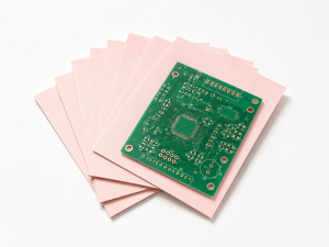
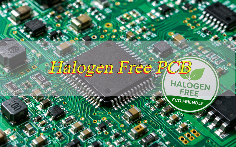
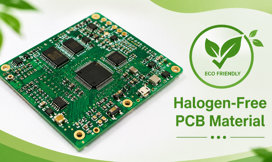
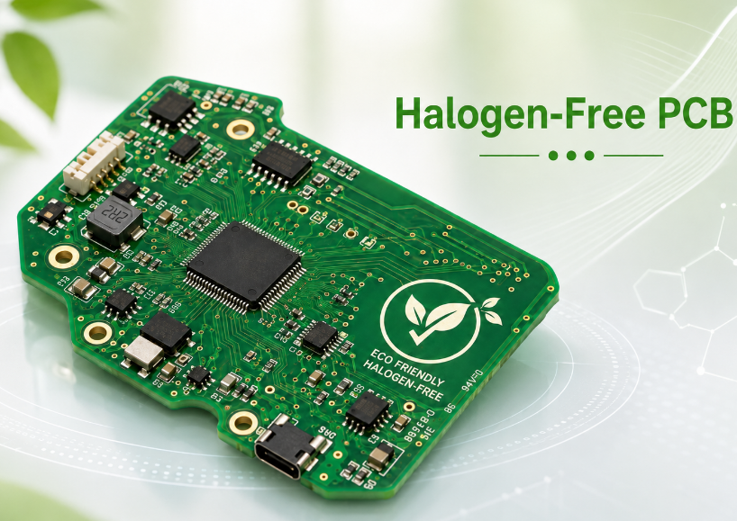
Halogen-free PCB material is used in electronics that require safer materials, environmental compliance and stable PCB manufacturing quality. It helps reduce harmful gas release during burning while keeping reliable flame resistance, soldering performance and long-term product stability.
This guide explains what halogen-free PCB material is, how it works, which standards matter, how to compare halogen-free FR4 and halogen-free CEM-3, and how to choose the right material for custom PCB manufacturing.
What Is Halogen-Free PCB Material?
Halogen-free PCB material refers to laminate, prepreg, solder mask and related board materials with controlled chlorine and bromine content. In common PCB manufacturing, a material is usually considered halogen-free when chlorine is no more than 900 ppm, bromine is no more than 900 ppm and total halogens are no more than 1500 ppm.
Traditional FR4 and CEM-3 materials may use brominated flame retardants to improve fire resistance. Halogen-free PCB material replaces these systems with phosphorus-based, nitrogen-based or inorganic flame-retardant systems. This helps maintain flame resistance while reducing toxic and corrosive gas release during combustion.
For custom PCB manufacturing, halogen-free does not mean lower performance. A suitable halogen-free PCB material can support UL 94 V-0 flame rating, lead-free soldering, multilayer construction, stable insulation resistance and long-term reliability. Final performance depends on laminate grade, resin system, stack-up design and production control.
Why Is Halogen-Free PCB Material Important in PCB Manufacturing?
Halogen-free PCB material is important because it supports safer, cleaner and more compliant electronics manufacturing. When halogenated materials burn, they may release corrosive and toxic gases. This can create risk in enclosed equipment, transportation electronics, consumer devices, industrial control systems and safety-related products.
Global market access is another key reason. Many OEM brands in Europe and North America prefer halogen free PCB materials for environmental policies, product safety rules and customer compliance requirements. In many export projects, halogen-free requirements are written directly into the PCB fabrication drawing, product specification or approved vendor list.
From a production view, halogen-free PCB material also affects processing. Resin chemistry, Tg, Td, CTE, drilling quality, lamination behavior and reflow resistance all influence yield. For OEM and ODM projects, early material confirmation helps reduce quotation errors, production delays and compliance risks during prototype, pilot run and mass production.
How Does Halogen-Free PCB Material Achieve Flame Resistance?
Halogen-free PCB material achieves flame resistance by using non-halogen flame-retardant systems instead of brominated or chlorinated additives. Common systems include phosphorus compounds, nitrogen-based chemistry, inorganic fillers and modified epoxy resin systems. These materials help slow ignition, promote char formation and reduce flame spread.
During combustion, phosphorus-based systems can form a protective char layer on the material surface. This layer limits oxygen contact and slows heat transfer into the laminate. Inorganic fillers can also help absorb heat and reduce the release of flammable gases from the resin system.
The main challenge is balance. A halogen-free PCB material must keep flame resistance without weakening dielectric performance, peel strength, drilling quality or reflow reliability. For this reason, low-cost halogen-free laminate is not always suitable for dense multilayer PCB, high-speed circuits or high-temperature applications.
What Standards and Compliance Limits Define Halogen-Free PCB Materials?
Halogen-free PCB material is usually defined by chemical content limits and supported by PCB material, flame resistance and environmental compliance standards. The most common limit is Cl ≤900 ppm, Br ≤900 ppm and total halogens ≤1500 ppm. These values are often used in laminate certificates, customer specifications and material declarations.
| Standard | Scope | Key Requirement |
|---|---|---|
| IEC 61249-2-21 | PCB base materials | Cl ≤900 ppm, Br ≤900 ppm, total halogens ≤1500 ppm |
| IPC-4101 | Rigid laminate and prepreg | Material type, resin system, Tg, Td, Dk, Df, flammability |
| IPC-4103 | High-speed laminate | Electrical and material performance classification |
| UL 94 V-0 | Flammability | Self-extinguishing behavior |
| RoHS | Restricted substances | Hazardous substance control |
| REACH | Chemical safety | Chemical registration and substance control |
| IPC-1752 | Material declaration | Supply chain material reporting |
For production drawings, it is better to state the requirement clearly instead of writing only “FR4.” A stronger callout is “compliant with IEC 61249-2-21, UL 94 V-0, lead-free compatible.” For critical projects, the drawing may also list a specific laminate brand, IPC slash sheet or approved equivalent.
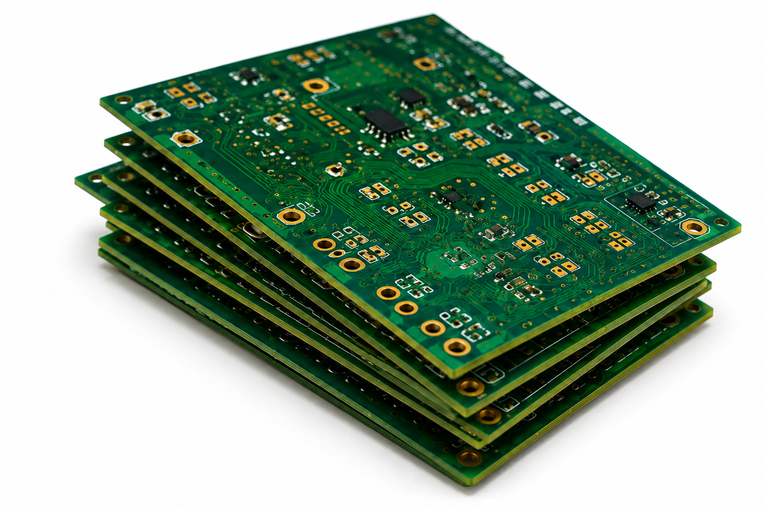
What Are the Main Types of Halogen-Free PCB Materials?
Halogen-free PCB material is not one single material. It includes several laminate families for different cost, reliability and performance targets. The correct option depends on board layers, operating temperature, assembly process, electrical speed and end-product compliance.
- Standard FR4 option
Used for most custom PCB manufacturing projects. It supports rigid PCB, multilayer PCB, lead-free soldering and many commercial or industrial electronics. - High-Tg FR4 option
Suitable for higher thermal stress, multilayer boards, power electronics and products exposed to repeated reflow or elevated operating temperature. - CEM-3 option
Often used for cost-sensitive single-sided or double-sided boards. It can be considered for appliances, LED products and simple control boards. - High-speed material option
Used when signal integrity matters. These materials offer controlled Dk and Df for data communication, computing, wireless and RF-related boards. - Metal core material option
Used for LED lighting, power modules and heat-dissipation applications where thermal management is more important than layer count. - Flexible or rigid-flex option
Used in compact electronics, wearable products and modules that require bending, folding or space-saving assembly.
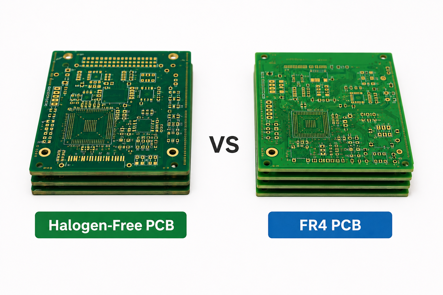
Halogen-Free FR4 vs Halogen-Free CEM-3: Which Material Is Better for Your PCB Project?
Halogen-free FR4 and halogen-free CEM-3 are both used in custom PCB manufacturing, but they are suitable for different project levels. FR4 is usually better for multilayer boards, higher reliability and stronger thermal performance. CEM-3 is more suitable for simpler boards where cost control is more important than high-density routing or harsh operating conditions.
| Item | Halogen-Free FR4 | Halogen-Free CEM-3 |
|---|---|---|
| Base Structure | Woven glass fabric with epoxy resin | Composite epoxy material with glass mat structure |
| Common Board Type | Multilayer PCB, double-sided PCB, industrial PCB | Single-sided PCB, double-sided PCB, simple control board |
| Mechanical Strength | Higher strength and better rigidity | Medium strength, suitable for less demanding boards |
| Thermal Stability | Better for lead-free soldering and repeated reflow | Suitable for lower thermal stress applications |
| Dimensional Stability | Better layer alignment and hole registration | Moderate stability, less suitable for tight tolerance designs |
| Electrical Performance | More stable for impedance and signal requirements | Suitable for general low-speed circuits |
| Drilling Quality | Better for dense holes and multilayer structures | Acceptable for simple hole structures |
| Moisture Resistance | Better when high-grade FR4 is selected | Usually lower than FR4 in humid or harsh environments |
| Routing Density | Medium to high routing density | Low to medium routing density |
| Reliability Level | Better for industrial, telecom, medical and automotive-related products | Better for cost-sensitive consumer or appliance products |
| Material Cost | Higher | Lower |
| Production Risk | More stable for complex structures | Lower cost, but higher risk in demanding projects |
| Best Fit | Reliability-focused custom PCB manufacturing | Cost-sensitive simple electronics |
For most medium and high-reliability PCB projects, FR4 is the safer and more flexible choice. It works better for multilayer boards, lead-free assembly, tighter tolerances, impedance control and long-term operation. If the project involves industrial control, telecom equipment, servers, automotive electronics or medical devices, FR4 is usually more suitable.
CEM-3 can be considered when the PCB structure is simple, the operating temperature is moderate and the product is highly cost-sensitive. It may be suitable for LED products, appliance control boards, simple consumer electronics and low-density double-sided boards. However, it should not be selected only because of lower cost if the project requires strong thermal reliability, stable dimensions or repeated soldering.
What Electrical, Thermal and Mechanical Properties Matter in Halogen-Free PCB Material?
The main properties of halogen-free PCB material include heat resistance, electrical stability, dimensional control and copper bonding strength. These properties affect soldering reliability, signal performance, via quality and long-term PCB durability. For custom PCB manufacturing, the material should match the board structure, assembly temperature and operating environment.
- Tg, Glass Transition Temperature
Tg shows when the resin system starts to soften under heat. A higher Tg helps the PCB keep better stability during lead-free soldering, lamination and long-term operation. For multilayer boards or high-temperature applications, high-Tg laminate is usually a safer choice. - Td, Decomposition Temperature
Td shows when the material starts to break down under high temperature. A higher Td gives the PCB better resistance to reflow soldering and repair work. Low Td may increase the risk of delamination, blistering and weak hole wall reliability. - CTE, Coefficient of Thermal Expansion
CTE shows how much the material expands when temperature changes. Lower Z-axis CTE helps protect plated through holes during soldering and field use. High CTE may cause via cracking, barrel separation and inner-layer connection failure. - Dk and Df
Dk affects impedance stability, while Df affects signal loss. Standard FR4 can work for general control boards. For high-speed, RF, telecom or data communication boards, stable Dk and low Df are more important. - Peel Strength
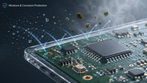
Peel strength shows how well copper foil bonds to the laminate. Higher peel strength helps prevent pad lifting, trace peeling and copper separation during soldering or rework. It is important for fine traces, connectors and heavy copper areas. - Moisture Absorption
Low moisture absorption helps reduce blistering, CAF risk, leakage current and delamination during high-temperature assembly. For humid environments, long storage or export projects, low-moisture material and proper baking control are important. - CTI, Comparative Tracking Index
CTI shows the material’s resistance to electrical tracking. Higher CTI improves insulation safety in power supplies, appliance electronics, industrial control boards and high-voltage areas.
For most commercial electronics, standard FR4 can meet basic requirements. For automotive electronics, power boards, telecom equipment, servers, medical devices or industrial control products, high-Tg, high-Td, low-CTE and low-moisture material is usually a better choice.
What Are the Advantages of Halogen-Free PCB Materials?
Halogen-free PCB materials offer environmental, safety and reliability benefits when selected correctly. The main value is not only “green material,” but also stronger compatibility with modern electronics compliance, lead-free assembly and brand safety requirements.
- Lower toxic and corrosive gas risk during fire or high-temperature decomposition.
- Better compliance support for products sold into regulated global markets.
- Suitable for lead-free soldering when high-Tg and high-Td grades are selected.
- Improved sustainability positioning for consumer and industrial products.
- Good material availability across FR4, high-Tg FR4, CEM-3 and high-speed laminates.
- Useful for enclosed equipment such as servers, automotive modules, railway systems and control cabinets.
- Supports custom PCB manufacturing from prototype to mass production when material data is confirmed early.
What Are the Limitations of Halogen-Free PCB Materials?
Halogen-free PCB materials also have limitations. Some grades may be more expensive, more sensitive to processing conditions or different in electrical behavior compared with traditional FR4. These issues can be controlled when the supplier reviews the stack-up and production process before fabrication.
- Higher material cost compared with standard brominated FR4 in many cases.
- Different drilling behavior depending on filler and resin chemistry.
- Possible dielectric variation that affects high-speed impedance design.
- More careful lamination control for multilayer boards.
- Material substitution risk if the drawing only says “halogen-free” without a grade.
- Longer procurement time for special high-speed or high-Tg laminate.
- Potential solder mask mismatch if only the base laminate is halogen-free but other materials are not specified.
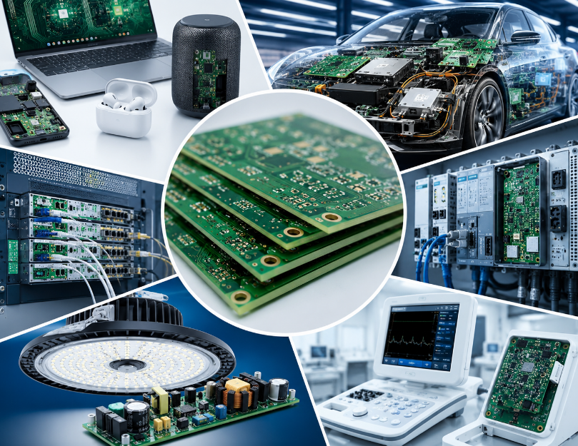
Where Are Halogen-Free PCB Materials Commonly Used?
Halogen-free PCB materials are used in products where safety, compliance, sustainability and long service life are important. Their application range continues to expand as more electronics brands move away from brominated flame-retardant systems.
- Consumer electronics
Smartphones, tablets, chargers, audio devices, smart home products and wearable electronics. - Automotive electronics
Body control modules, lighting boards, battery management systems, infotainment boards and sensor modules. - Industrial control
PLC boards, motor control boards, power control modules, automation equipment and monitoring devices. - Telecom and data equipment
Routers, switches, optical modules, servers, base station boards and high-speed communication modules. - LED and power electronics
LED lighting boards, power supplies, inverter control boards and thermal management PCB projects. - Medical and safety-related electronics
Monitoring equipment, control panels, portable devices and products with strict material declarations.
For example, an industrial control PCB project may switch from standard FR4 to high-Tg material when the board must pass lead-free reflow, long-term thermal cycling and export compliance review. In this situation, Tg, Td, CTE, laminate traceability and stable repeat production are more important than material cost alone.
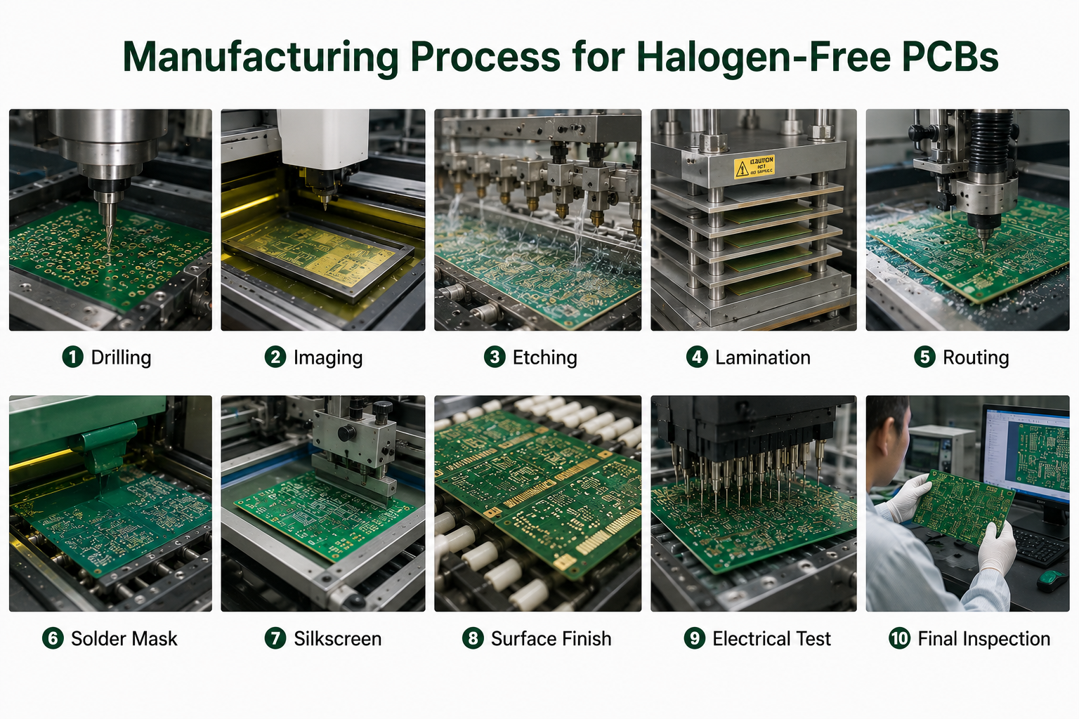
What Manufacturing Challenges Occur with Halogen-Free PCB Materials?
Halogen-free PCB material can bring process challenges during drilling, lamination, desmear, plating, solder mask application and final assembly. These challenges do not mean the material is difficult to use, but they require controlled manufacturing parameters.
Step 1: Material confirmation
The factory checks laminate grade, Tg, Td, copper thickness, resin content, IPC slash sheet, UL rating and material declaration before production. This step prevents incorrect material substitution and compliance disputes after delivery.
Step 2: Stack-up review
The stack-up is checked for board thickness, copper distribution, prepreg selection, impedance layers and press cycle suitability. For multilayer boards, lamination pressure and temperature control are especially important.
Step 3: Drilling control
Some laminates contain fillers that affect drill wear and hole wall quality. The factory may adjust drill parameters, hit count, feed rate and drill tool selection to reduce smear, burrs and rough hole walls.
Step 4: Desmear and plating control
Hole wall preparation should match the resin system. Incomplete desmear can reduce plating adhesion, while over-processing may attack the laminate surface. Stable copper plating reduces via cracking and hole reliability issues.
Step 5: Solder mask and surface finish matching
The solder mask, legend ink and surface finish should match the compliance requirement if the final product requires full material control. ENIG, HASL lead-free, immersion silver and OSP can be selected according to assembly and storage requirements.
Step 6: Assembly reliability review
Lead-free assembly often reaches higher peak temperatures. The material should withstand reflow without delamination, blistering, pad lifting or copper separation. This is especially important for double-sided SMT assembly and dense components.
In mass production, material review should be completed before releasing the job to the production line. A practical factory check usually includes laminate certificate review, press cycle suitability, drill quality, solder mask compatibility and assembly temperature profile. This helps reduce delamination, via cracking, material mismatch and repeat-order variation.
What Common Failure Risks Should Be Avoided in Halogen-Free PCB Projects?
Common failure risks in halogen-free PCB projects include delamination, blistering, CAF, via cracking, poor copper adhesion, solder mask mismatch and wrong material declaration. Most issues come from unclear specifications, poor material matching or weak process control.
| Risk | Common Cause | Prevention |
|---|---|---|
| Delamination | Low Td, moisture, poor lamination | Use suitable Tg/Td and bake when required |
| Blistering | Moisture absorption or surface contamination | Control storage, baking and cleaning |
| Via Cracking | High Z-axis expansion | Use low-CTE laminate and stable plating |
| CAF | Moisture, glass/resin interface weakness | Select CAF-resistant material and spacing rules |
| Pad Lifting | Weak copper adhesion or high thermal stress | Check peel strength and assembly profile |
| Impedance Drift | Wrong Dk/Df assumption | Confirm laminate data before stack-up approval |
| Compliance Failure | Unclear material callout | Specify IEC limits and material declaration |
| Solder Mask Conflict | Base laminate only | Confirm solder mask and ink compliance |
A practical factory approach is to review the risk before production rather than after inspection. For example, a six-layer industrial PCB with lead-free reflow should not use the same material logic as a simple two-layer consumer board. The board structure, soldering temperature and operating environment must be reviewed together.
How Is Halogen-Free PCB Material Tested During PCB Production?
Halogen-free PCB material is tested through material verification, process inspection and finished board checks. The goal is to confirm that the selected material meets compliance requirements and can remain stable during PCB manufacturing, soldering and long-term use.
- Material certificate review
The factory checks laminate datasheets, material declarations, RoHS/REACH statements and UL information before production. This helps confirm whether the material meets Cl ≤900 ppm, Br ≤900 ppm and total halogens ≤1500 ppm. - Incoming material inspection
The laminate, prepreg and copper-clad material should be checked before production. The factory confirms material grade, thickness, copper weight, surface condition and batch information to avoid wrong material use. - Stack-up and laminate verification
For multilayer boards, the stack-up should be reviewed before lamination. This includes layer structure, dielectric thickness, copper balance and pressing suitability. Good stack-up control helps reduce warpage, delamination and registration problems. - Drilling and hole quality check
Some laminates may have different drilling behavior from standard FR4. The factory checks hole wall quality, smear, burrs and drill accuracy. Poor drilling control can affect plating adhesion and via reliability. - Plating and microsection inspection
Microsection inspection helps check hole wall plating, copper thickness, inner-layer connection and laminate condition. This is important for multilayer PCB, high-reliability boards and products that require long service life. - Thermal stress testing
Thermal stress testing checks whether the PCB can withstand soldering heat without blistering, delamination or copper separation. This is especially important for lead-free assembly, double-sided SMT and high-Tg FR4 projects. - Electrical testing
Finished boards should pass open and short testing. For impedance-controlled boards, impedance testing should also be performed according to the approved stack-up and actual material data. - Solderability testing
Solderability testing confirms whether pads can be soldered properly after surface finish processing. It helps reduce assembly problems such as poor wetting, weak solder joints and rework risk. - Final quality inspection
Final inspection checks board appearance, dimensions, solder mask, marking, surface finish, hole quality and customer requirements. For export or repeat orders, inspection records and material batch information should be kept for traceability.
For reliable production, testing should not be treated as a final step only. A good factory controls material from incoming review to finished board inspection, so prototype, pilot run and mass production can remain consistent.
What Quality Standards Should Halogen-Free PCB Production Follow?
Halogen-free PCB production should follow material, process and finished board quality standards. These standards help ensure that the PCB is not only compliant in material declaration, but also stable in manufacturing and reliable in final application.
| Standard | Production Focus |
|---|---|
| IEC 61249-2-21 | Halogen-free content limits |
| IPC-4101 | Rigid laminate and prepreg requirements |
| IPC-6012 | Rigid PCB qualification and performance |
| IPC-A-600 | Printed board acceptability |
| IPC-A-610 | Assembly acceptability when PCBA is supplied |
| UL 94 V-0 | Flame resistance classification |
| RoHS | Restricted hazardous substances |
| REACH | Chemical substance compliance |
| ISO 9001 | Quality management system |
| IATF 16949 | Automotive quality control when applicable |
| ISO 13485 | Medical production control when applicable |
For export manufacturing, the supplier should provide clear documentation instead of vague claims. Useful documents include material datasheet, laminate certificate, UL file information, RoHS/REACH statement, microsection report, impedance report and final inspection report. These records help purchasing teams, quality teams and end customers confirm that the approved material and finished PCB meet the required specification.
What Factors Affect the Cost of Halogen-Free PCB Manufacturing?
The cost of halogen-free PCB manufacturing depends on material grade, board structure, production difficulty, testing requirements and order quantity. Halogen-free laminate is usually more expensive than standard FR4, but the final PCB cost is mainly decided by the full manufacturing specification.
- Material grade
Standard FR4 is more cost-effective than high-Tg, low-Df or high-speed laminate. If the project requires high thermal stability, controlled impedance or low signal loss, the material cost will increase. - Layer count
A two-layer board is easier to produce than a four-layer, six-layer or high-layer-count PCB. More layers require more lamination steps, tighter stack-up control and more inspection, so the manufacturing cost becomes higher. - Board thickness and copper weight
Special board thickness, heavy copper or uneven copper distribution can increase production difficulty. Heavy copper also requires more careful etching, plating and thermal control, especially for power-related projects. - Surface finish
OSP is usually more economical, while ENIG, immersion silver and other finishes may increase cost. The surface finish should match soldering requirements, storage time, component type and end-use environment. - Impedance control
If the PCB requires controlled impedance, the supplier must calculate stack-up, confirm material Dk/Df and perform impedance testing. This adds engineering work, material control and inspection cost. - Tolerance requirements
Tight line width, small spacing, small holes, controlled thickness and high registration accuracy increase manufacturing difficulty. These requirements are common in dense multilayer boards and high-performance electronics. - Testing and inspection level
Basic boards may only require standard electrical testing and visual inspection. High-reliability projects may require microsection reports, thermal stress testing, solderability testing, ionic contamination testing, impedance reports or material traceability records. - Order quantity and lead time
Prototype orders usually have higher unit cost because setup, tooling and engineering review are spread across fewer boards. Mass production can reduce unit cost, while urgent delivery may increase production and material procurement cost.
For cost control, the best approach is to match the material to the real application risk. A simple consumer board may not require high-end laminate, while a dense industrial or telecom PCB should not use low-grade material only to reduce cost.
How to Choose a Reliable Halogen-Free PCB Manufacturer?
A reliable halogen-free PCB manufacturer should provide stable material sourcing, strict process control, clear compliance documents and repeatable production quality. For OEM, ODM, prototype and mass production projects, the manufacturer should not only supply the material, but also control fabrication, testing, documentation and delivery.
- Check material compliance capability
The manufacturer should confirm whether the selected material meets IEC 61249-2-21, RoHS, REACH and UL 94 V-0 requirements when applicable. Material datasheets, laminate certificates and material declarations should be available before production. - Review PCB manufacturing experience
Halogen-free PCB material may require different drilling, lamination, plating and soldering control compared with standard FR4. A capable manufacturer should understand high-Tg FR4, CEM-3, multilayer PCB, impedance control and lead-free assembly requirements. - Confirm material traceability
For export products and repeat orders, traceability is important. The manufacturer should be able to track laminate batch, copper thickness, production lot, inspection records and final delivery documents. - Evaluate engineering review ability
A good manufacturer should review stack-up, material grade, surface finish, impedance requirements and production risks before fabrication. This helps reduce wrong material selection, delamination, via cracking, quotation errors and delivery delays. - Check quality control process
The manufacturer should support electrical testing, visual inspection, microsection checks, solderability testing, thermal stress testing and final inspection reports. For high-reliability boards, testing requirements should be confirmed before production starts. - Compare prototype and mass production capability
A reliable manufacturer should keep quality stable from samples to pilot run and mass production. Material consistency, process repeatability and batch control are important for long-term supply. - Review export and delivery support
For international buyers, the manufacturer should provide clear communication, export packaging, shipping support and complete production documents. A China source factory can offer flexible customization, cost control and global delivery without making false local claims. - Avoid choosing by price only
The lowest price may hide risks in material grade, testing level, documentation or process control. A reliable halogen-free PCB manufacturer should balance cost, quality, compliance, delivery and engineering support.
What Files and Specifications Are Needed Before Halogen-Free PCB Production?
Before halogen-free PCB production, clear files and specifications help the supplier quote accurately, select the right material and reduce production risk. Missing information may cause wrong material use, quotation delays or compliance issues after delivery.
- Gerber files
Include copper layers, solder mask, silkscreen, outline and all required board layers. - Drill files
Show plated holes, non-plated holes, slots and special hole requirements. - Stack-up
Provide layer order, dielectric thickness, copper weight and total board thickness. - Material requirement
Clearly state the required material type. For stricter projects, add Tg, UL rating or halogen-free limits. - Surface finish
Confirm ENIG, OSP, HASL lead-free, immersion silver or other required finish. - Copper thickness
State base copper and finished copper thickness, especially for power boards or heavy copper projects. - Impedance data
If controlled impedance is required, provide target impedance, tolerance and reference layers. - Solder mask requirement
Confirm whether solder mask and legend ink also require compliance control. - Quantity and lead time
State whether the order is for prototype, pilot run or mass production. - Quality requirements
Confirm IPC class, electrical test, microsection report, impedance report or other inspection needs. - Assembly files
If PCBA is required, provide BOM, CPL, assembly drawing and soldering requirements.
A clear note can be written as: “Use material compliant with IEC 61249-2-21, Cl ≤900 ppm, Br ≤900 ppm, total halogens ≤1500 ppm, UL 94 V-0, lead-free assembly compatible.”
FAQs About Halogen-Free PCB Material
Q1: Is halogen-free PCB material the same as RoHS-compliant PCB material?
A1: No. RoHS controls restricted hazardous substances, while halogen-free focuses on chlorine and bromine content. A PCB can be RoHS-compliant but not halogen-free, so both requirements should be listed clearly when the project requires full compliance.
Q2: What is the standard halogen-free limit for PCB materials?
A2: The common limit is chlorine ≤900 ppm, bromine ≤900 ppm and total halogens ≤1500 ppm. This limit should be written in the fabrication drawing or material specification to avoid vague material selection.
Q3: Does halogen-free PCB material have weaker flame resistance than standard FR4?
A3: Not necessarily. A suitable laminate can still meet UL 94 V-0 flame resistance. The key is to confirm the laminate datasheet, UL rating and flame-retardant system before PCB production.
Q4: Is halogen free FR4 PCB material suitable for multilayer boards?
A4: Yes. Halogen free FR4 PCB material is widely used for multilayer PCB manufacturing. For dense boards, high layer counts or lead-free assembly, high-Tg and high-Td grades are usually better.
Q5: When should I choose halogen-free CEM-3 PCB material?
A5: Choose halogen-free CEM-3 PCB material for simple, cost-sensitive single-sided or double-sided boards. For multilayer boards, high thermal stress or tight dimensional control, FR4 is usually the safer choice.
Q6: Are halogen free PCB materials more expensive?
A6: Usually yes. Halogen free PCB materials often cost more than standard FR4, especially high-Tg, low-Df or special-grade laminates. However, they can reduce compliance risk and improve export project acceptance.
Q7: Can a PCB be partially halogen-free?
A7: Yes. A PCB may use halogen-free laminate but non-halogen-free solder mask, ink or adhesive. If full board compliance is required, the complete material system should be confirmed before production.
Q8: What failure problems are common with poor halogen-free PCB material selection?
A8: Common risks include delamination, blistering, via cracking, CAF, pad lifting, impedance drift and poor soldering reliability. These issues can often be reduced by reviewing Tg, Td, CTE, Dk, Df and process suitability before fabrication.
Q9: Is halogen-free PCB material suitable for high-speed circuits?
A9: Yes, but the grade matters. High-speed circuits require stable Dk, low Df and controlled impedance. Standard FR4 may work for moderate-speed boards, while high-speed applications should use suitable low-loss laminate.
Q10: How should I write halogen-free PCB material in a fabrication drawing?
A10: Use a clear note such as “Compliant with IEC 61249-2-21, Cl ≤900 ppm, Br ≤900 ppm, total halogens ≤1500 ppm, UL 94 V-0, lead-free compatible.” Add the laminate grade if the project has strict reliability requirements.
Q11: Does halogen-free PCB material affect soldering performance?
A11: Yes, it can. Tg, Td, moisture absorption and Z-axis CTE affect soldering reliability. For lead-free assembly, the supplier should confirm material heat resistance, baking control, surface finish and reflow compatibility.
Q12: What documents should a supplier provide for halogen-free PCB production?
A12: A supplier should provide material datasheets, material declaration, RoHS/REACH statement, UL information, final inspection report and testing records. For high-reliability boards, microsection and impedance reports may also be required.
How Can You Start a Halogen-Free PCB Manufacturing Project?
A successful halogen-free PCB manufacturing project starts with clear material requirements and early production review. Before quotation, prepare Gerber files, stack-up, material notes, surface finish, quantity, testing requirements and assembly files if PCBA service is required.
For most projects, FR4 is a safe choice for reliability, while CEM-3 can be used for simpler cost-sensitive boards. If your project requires OEM manufacturing, ODM production, samples or mass production, contact our team for fast technical review and quotation support: sales@bestpcbs.com.