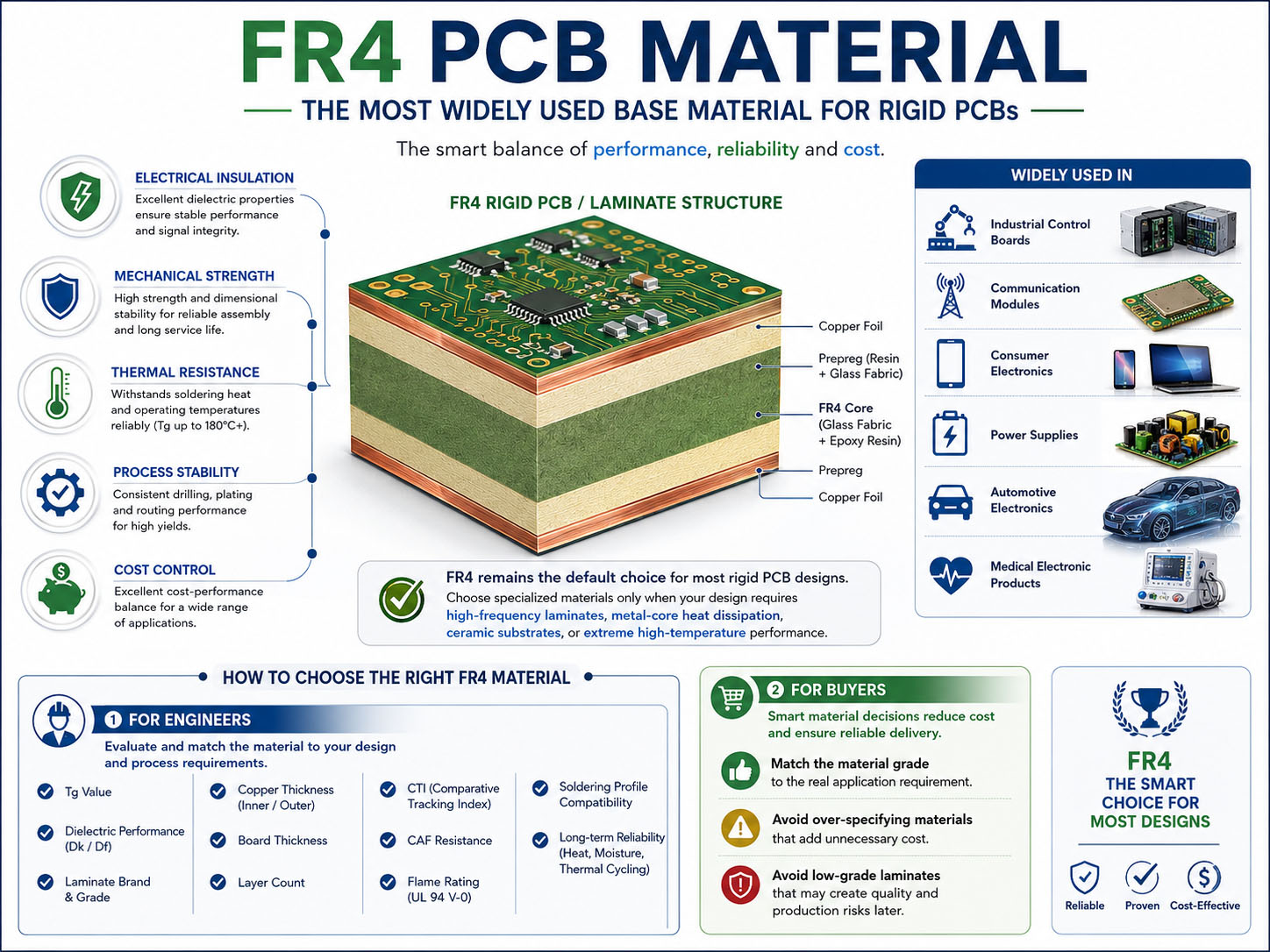
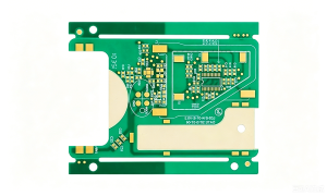
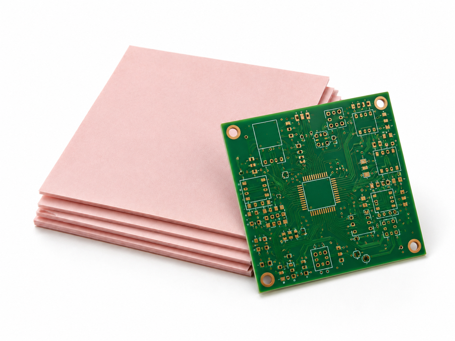
High-Tg PCB materials are used when a printed circuit board must remain dimensionally stable under heat, soldering stress, continuous operation, or demanding environmental conditions. In many PCB projects, standard FR4 is sufficient. However, when the board faces lead-free reflow, high layer count, power density, automotive temperature cycling, or long-term reliability requirements, high-Tg PCB materials become a safer engineering choice.
For engineers, Tg is not just a number on a laminate datasheet. It affects expansion behavior, via reliability, delamination resistance, impedance stability, soldering performance, and production yield. For buyers, the key is to match the Tg grade with the real application instead of overpaying for unnecessary specifications or choosing a laminate that cannot support the product’s operating environment.
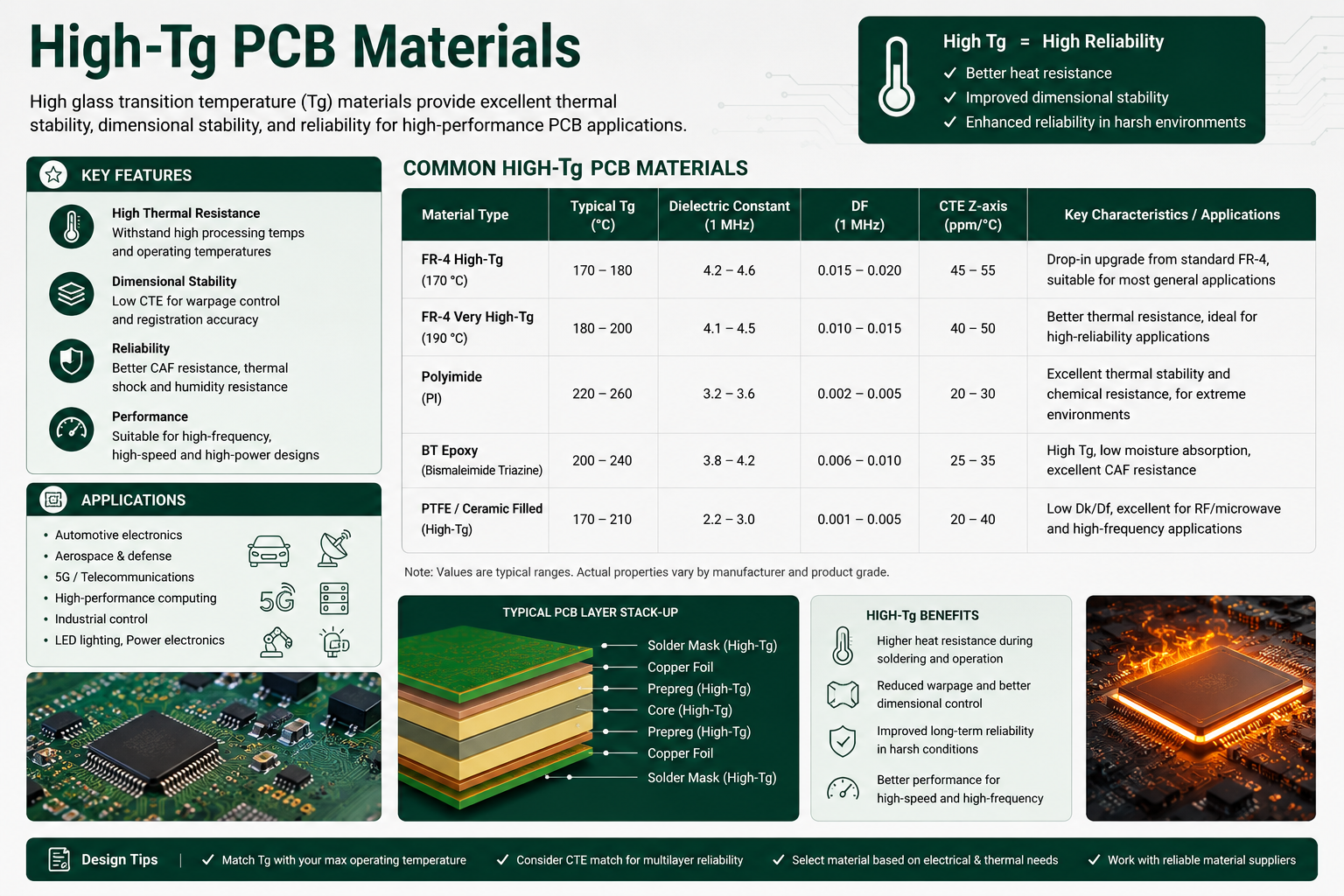
What Are High-Tg PCB Materials?
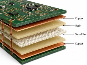
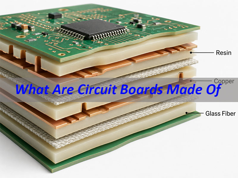
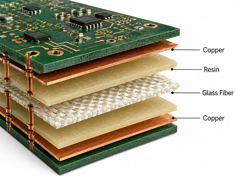
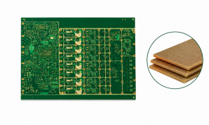
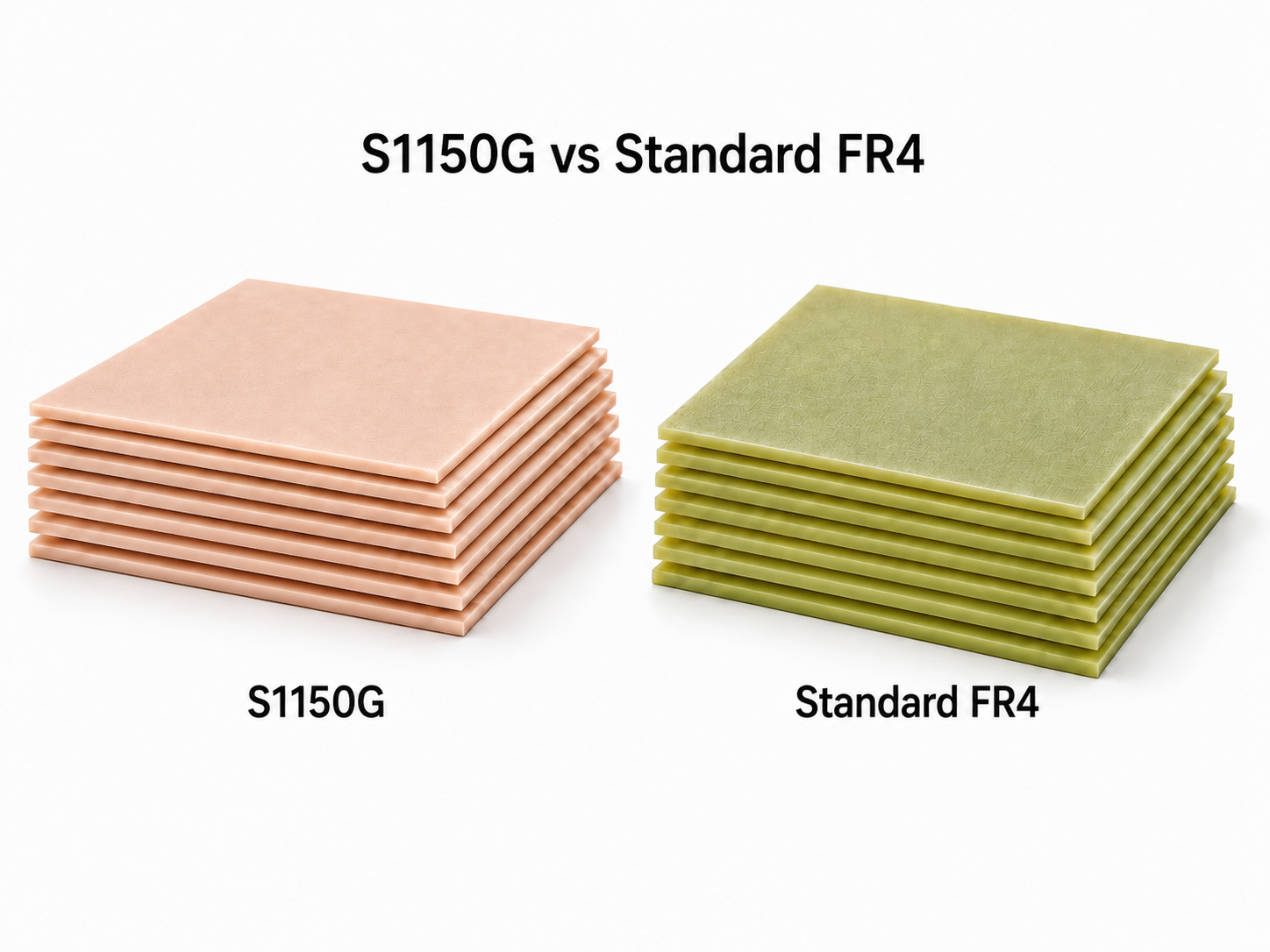
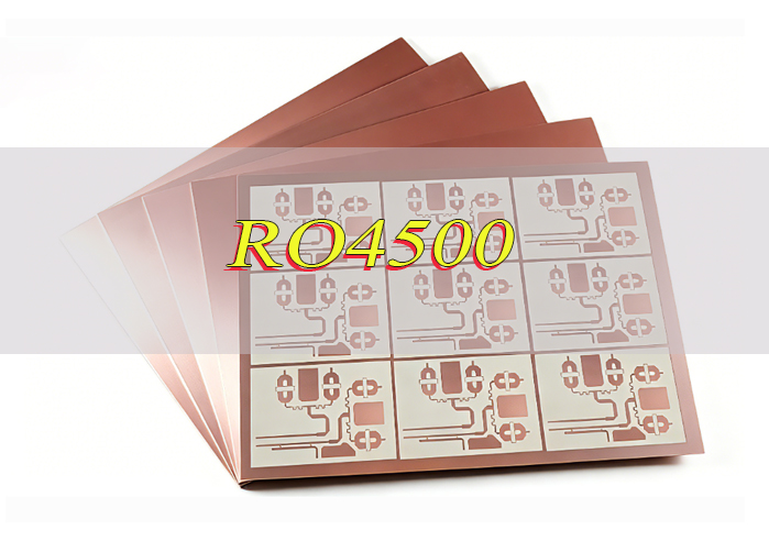
High-Tg PCB materials are PCB laminates with a higher glass transition temperature than standard FR4 materials. Tg means “glass transition temperature.” It refers to the temperature range where the resin system changes from a rigid glass-like state to a softer rubber-like state.
In PCB manufacturing, Tg is important because the board does not immediately fail when it reaches this temperature range. Instead, its mechanical behavior changes. Above Tg, the laminate expands faster, especially in the Z-axis direction. This can stress plated through holes, vias, copper barrels, inner-layer connections, and solder joints.
Standard FR4 material often has a Tg of around 130–140°C. High-Tg FR4 usually refers to materials with a Tg of around 170°C or higher. Some advanced laminate systems may reach 180°C, 200°C, or above, depending on resin chemistry and application requirements.
In simple terms, high-Tg PCB materials are base materials designed to maintain better mechanical and thermal stability when exposed to higher processing or operating temperatures.
Why Are High-Tg PCB Materials Important?
High-Tg PCB materials are important because modern PCB assemblies often experience more heat than older electronic products. Lead-free soldering requires higher reflow temperatures. Compact electronic designs place more components into smaller spaces. Power devices, LEDs, motor drivers, battery systems, and RF modules all create localized thermal stress.
When a PCB material has an insufficient Tg rating, the board may show warpage, delamination, pad lifting, barrel cracking, or degraded electrical performance after soldering or long-term use. These issues are especially costly in automotive electronics, industrial control, medical devices, aerospace modules, energy systems, and communication equipment.
High-Tg materials help improve:
| Performance Area | Why It Matters |
|---|---|
| Thermal Stability | Reduces deformation during reflow and operation |
| Via Reliability | Helps protect plated through holes under thermal cycling |
| Dimensional Control | Supports tighter registration in multilayer boards |
| Delamination Resistance | Improves laminate integrity during heat exposure |
| Long-Term Durability | Supports products used in harsh or high-duty environments |
| Assembly Yield | Reduces process risk during lead-free soldering |
For high-reliability PCBs, Tg is usually reviewed together with decomposition temperature, CTE, copper thickness, layer count, board thickness, soldering profile, and operating temperature.
How Do High-Tg PCB Materials Work Under Heat?
High-Tg PCB materials work by using resin systems that remain mechanically stable at higher temperatures. The resin, glass fiber, copper foil, and curing system must work together to resist expansion, softening, moisture stress, and thermal fatigue.
Before the laminate reaches Tg, the board stays relatively rigid. Once the temperature passes Tg, the resin becomes more flexible and its expansion rate increases. This expansion is especially important in the Z-axis direction because vias and plated through holes pass vertically through the board.
If Z-axis expansion becomes excessive, copper barrels can stretch. Repeated heating and cooling may create micro-cracks. In multilayer boards, inner-layer connections may also become vulnerable if material selection, drilling, plating, and lamination are not well controlled.
High-Tg materials help reduce this risk by keeping the resin system more stable at elevated temperatures. They do not make the PCB immune to heat, but they provide a wider process and reliability margin.
Tg is not the same as maximum operating temperature. It is one important thermal property used to evaluate how a PCB laminate behaves under heat.
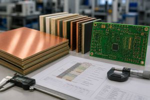
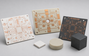
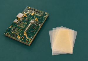
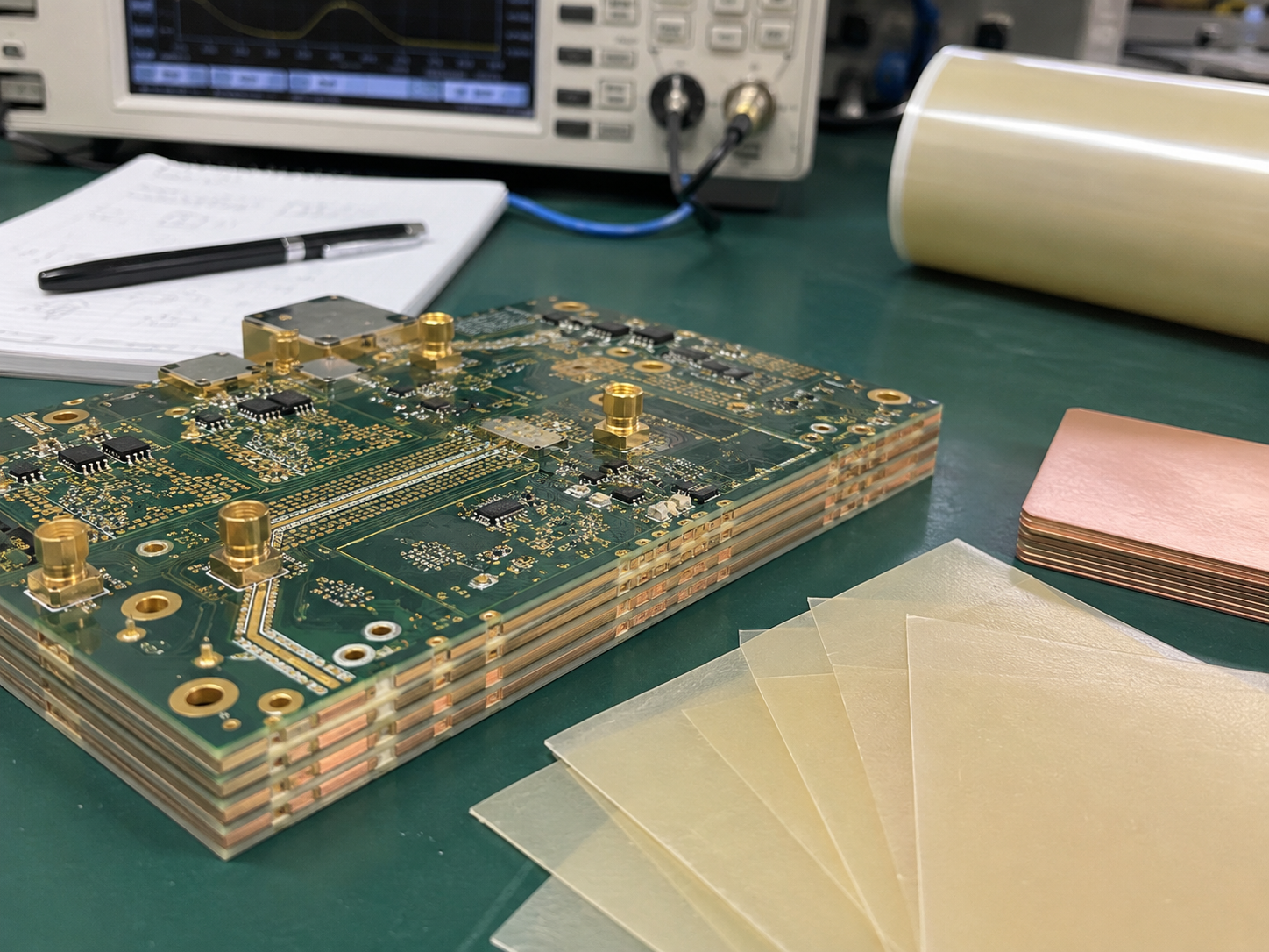
Common Types of High-Tg PCB Materials
High-Tg PCB materials are available in different material families. The right choice depends on electrical performance, thermal load, mechanical requirements, cost target, and application environment.
| Material Type | Typical Tg Range | Common Use |
|---|---|---|
| High-Tg FR4 | 170–180°C | Industrial, automotive, medical, and multilayer PCBs |
| Halogen-Free High-Tg FR4 | 170–180°C | Products requiring environmental compliance |
| High-Performance FR4 | 180°C+ | Dense multilayer, lead-free assembly, and high-reliability electronics |
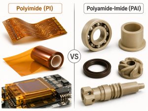
| Polyimide | 250°C+ depending on grade | Aerospace, high-temperature, flex, and rigid-flex designs |
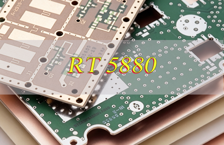
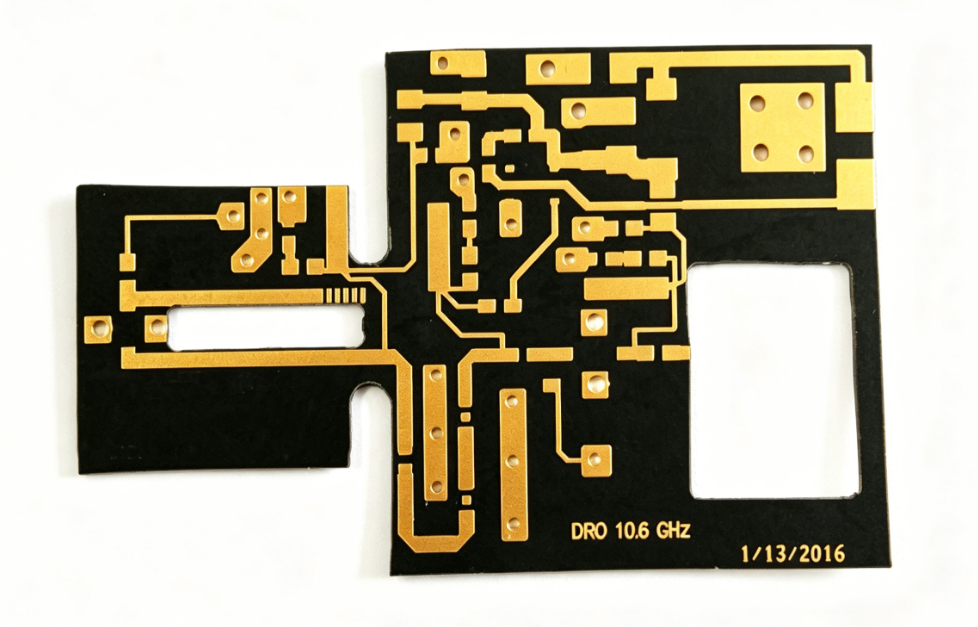
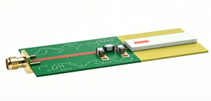
| Rogers / High-Frequency Laminate | Varies by material | RF, microwave, antenna, radar, and communication modules |
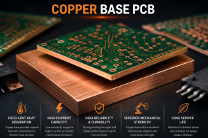
| Metal-Core PCB Material | Depends on dielectric system | LED lighting, power electronics, and thermal management |
| Ceramic PCB Material | Very high thermal stability | Power modules, high-power LED, laser, sensor, and RF applications |
For most rigid PCB projects, high-Tg FR4 is the practical first choice. It offers better thermal endurance than standard FR4 while keeping fabrication cost and process compatibility under control.
For extreme temperature, RF performance, or high thermal conductivity, engineers may need polyimide, Rogers, metal-core, or ceramic substrates instead of high-Tg FR4.
High-Tg FR4 vs Standard FR4 vs Advanced PCB Materials
Not every product needs high-Tg material. Standard FR4 remains suitable for many consumer, low-power, and moderate-temperature applications. The decision should be based on actual design risk, not only on the desire to use a “better” material.
| Material | Main Strength | Limitation | Best Fit |
|---|---|---|---|
| Standard FR4 | Cost-effective and widely available | Lower thermal margin | General electronics |
| High-Tg FR4 | Better thermal stability and assembly reliability | Higher cost than standard FR4 | Multilayer, automotive, industrial, and medical PCBs |
| Polyimide | Excellent high-temperature resistance | More expensive and process-sensitive | Aerospace, high-temperature, flex, and rigid-flex designs |
| Rogers Laminate | Stable dielectric performance | Higher material and process cost | RF, antenna, and microwave circuits |
| Aluminum PCB | Good heat spreading | Limited routing structure | LED and power modules |
| Ceramic PCB | High thermal conductivity and stability | Higher cost and specialized processing | High-power, high-frequency, and high-reliability modules |
A common engineering mistake is selecting high-Tg FR4 when the real issue is heat dissipation. Tg improves thermal stability, but it does not replace thermal design. If the circuit generates significant heat, copper weight, thermal vias, copper planes, metal-core materials, or ceramic substrates may also be required.
Key Properties Engineers Should Check
Tg is important, but it should not be checked alone. A laminate with a high Tg value can still perform poorly if other thermal or electrical properties do not match the design.
Glass Transition Temperature
Tg indicates when the resin system begins to change mechanical behavior. A higher Tg gives the board a wider thermal process margin, especially for lead-free soldering and high-temperature operation.
CTE
CTE means coefficient of thermal expansion. Z-axis CTE is critical because plated holes and vias are exposed to vertical expansion stress. Lower and more stable CTE helps improve via reliability.
Td
Td means decomposition temperature. It indicates when the resin begins to chemically degrade. A material with good Tg but low Td may still be risky during multiple reflow cycles or harsh processing.
T288
T288 measures how long a laminate can withstand 288°C before delamination under test conditions. It is useful for evaluating resistance to lead-free assembly temperatures.
CAF Resistance
CAF means conductive anodic filament. It is an electrochemical failure path that can occur inside the laminate under voltage, humidity, and contamination. CAF resistance matters for dense designs, fine spacing, and high-reliability electronics.
Dielectric Constant and Loss Tangent
For impedance-controlled, RF, and high-speed circuits, Dk and Df stability must be reviewed. High Tg alone does not guarantee signal integrity.
Moisture Absorption
Moisture trapped inside the laminate can expand during soldering and increase the risk of delamination or blistering. Low moisture absorption supports better assembly reliability.
When Should You Use High-Tg PCB Materials?
High-Tg PCB materials are recommended when the PCB will face higher thermal stress during production, operation, or field use. They are also suitable when product reliability is more important than the lowest possible board cost.
You should consider high-Tg material when the PCB has:
| Project Condition | Why High-Tg Material Helps |
|---|---|
| Lead-Free Reflow | Higher peak temperature increases laminate stress |
| Multilayer Stackup | More lamination pressure and thermal expansion risk |
| Thick Board Design | Higher Z-axis stress around plated holes |
| High Copper Weight | More thermal mass and process stress |
| Fine-Pitch Components | Better dimensional stability supports assembly accuracy |
| Automotive Temperature Cycling | Improves long-term mechanical reliability |
| Power Electronics | Supports higher thermal exposure around power areas |
| Industrial Equipment | Improves durability under continuous operation |
| Medical Electronics | Supports stable production and documentation control |
| Aerospace or UAV Electronics | Helps withstand demanding reliability conditions |
High-Tg material is especially valuable when a PCB must pass repeated thermal cycles, multiple soldering processes, rework exposure, or long operating life requirements.
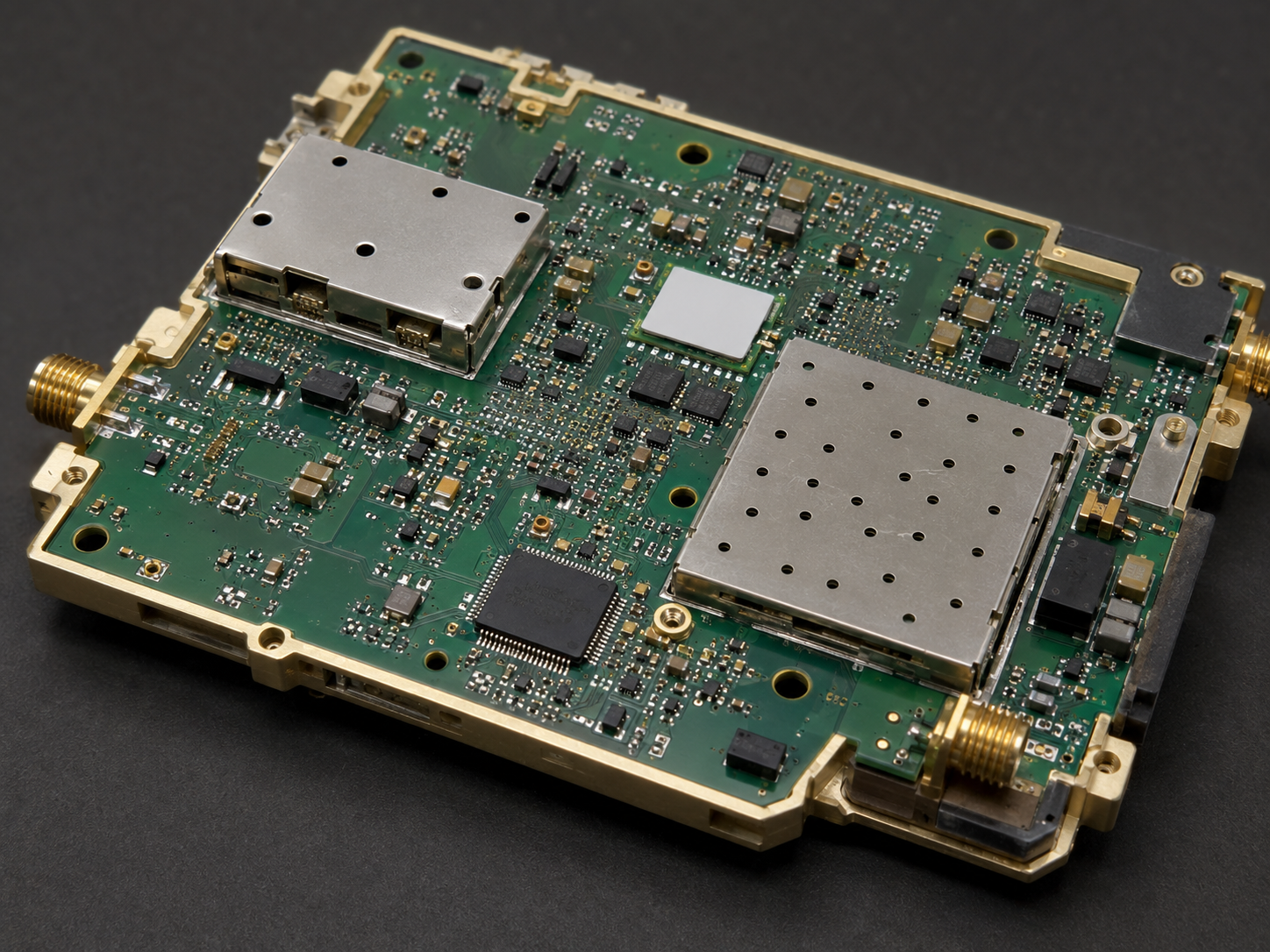
Where Are High-Tg PCB Materials Used?
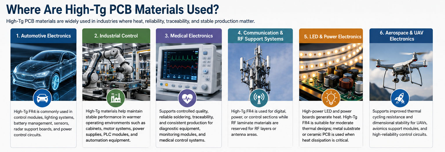
High-Tg PCB materials are widely used in industries where heat, reliability, traceability, and stable production matter.
Automotive Electronics
Automotive boards often face temperature cycling, vibration, high current, and long service life requirements. High-Tg FR4 is commonly used in control modules, lighting systems, battery management, sensors, radar support boards, and power control circuits.
Industrial Control
Industrial PCBs may operate continuously in cabinets, motor systems, power supplies, PLC modules, and automation equipment. High-Tg materials help maintain stable performance in warmer operating environments.
Medical Electronics
Medical PCB projects often require controlled quality, reliable soldering, traceability, and consistent production documentation. High-Tg material can support stable assembly for diagnostic equipment, monitoring modules, and medical control systems.
Communication and RF Support Systems
Not all communication boards require RF laminates throughout the entire design. Some products use high-Tg FR4 for digital, power, or control sections while reserving special materials for RF layers or antenna areas.
LED and Power Electronics
High-power LED and power boards generate localized heat. High-Tg FR4 can help in moderate thermal designs, while aluminum, copper substrate, or ceramic PCB may be selected when heat dissipation becomes the primary requirement.
Aerospace and UAV Electronics
For UAVs, avionics support modules, and high-reliability control circuits, high-Tg materials support improved thermal cycling resistance and dimensional stability during fabrication.
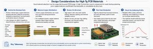
Design Considerations for High-Tg PCB Materials
Good material selection must be supported by good PCB design. A high-Tg laminate cannot compensate for weak stackup planning, poor copper balance, insufficient thermal paths, or unsuitable via structure.
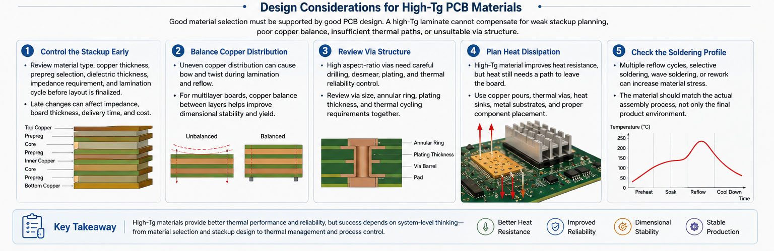
Control the Stackup Early
Material type, copper thickness, prepreg selection, dielectric thickness, impedance requirement, and lamination cycle should be reviewed before layout is finalized. Late changes can affect impedance, board thickness, delivery time, and cost.
Balance Copper Distribution
Uneven copper distribution can cause bow and twist during lamination and reflow. For multilayer boards, copper balance between layers helps improve dimensional stability and manufacturing yield.
Review Via Structure
High aspect-ratio vias need careful drilling, desmear, plating, and thermal reliability control. For high-reliability boards, via size, annular ring, plating thickness, and thermal cycling requirements should be reviewed together.
Plan Heat Dissipation
High-Tg material improves heat resistance, but heat still needs a path to leave the board. Copper pours, thermal vias, heat sinks, metal substrates, and component placement must be considered.
Check the Soldering Profile
Multiple reflow cycles, selective soldering, wave soldering, or rework can increase material stress. The material should match the actual assembly process, not only the final product environment.
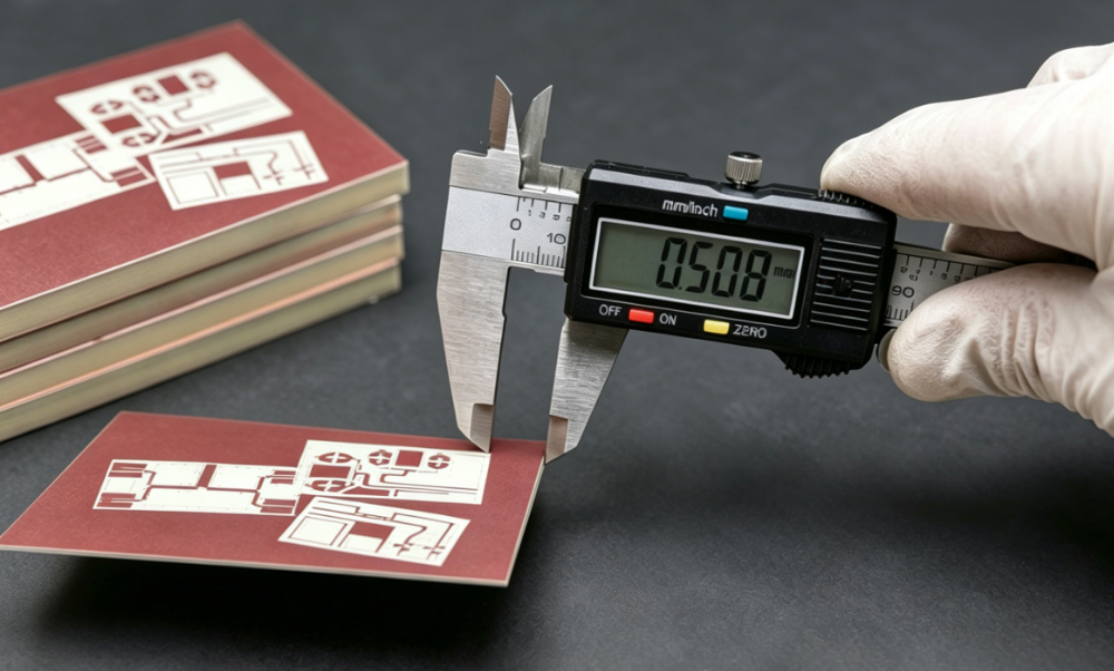
Manufacturing Challenges and Factory Control Points
High-Tg PCB materials require controlled fabrication because material stiffness, resin behavior, drilling response, and lamination conditions may differ from standard FR4.
Lamination Control
High-Tg laminates may need specific lamination temperature, pressure, and cure control. Incorrect lamination can lead to voids, weak bonding, thickness deviation, or delamination risk.
Drilling Quality
The drilling process affects hole wall quality and later plating reliability. High-Tg materials may be harder or more abrasive, so drill bit condition, feed rate, spindle speed, and hole cleaning must be managed.
Desmear and Plating
After drilling, resin smear must be removed before copper plating. Poor desmear can create weak via connections. Plating thickness and uniformity are critical for boards exposed to thermal cycling.
Solder Mask and Surface Finish
ENIG, OSP, HASL, immersion silver, and other finishes should be selected according to assembly process, shelf life, solderability, fine-pitch components, and application environment.
Final Inspection
AOI, electrical testing, impedance testing, microsection analysis, solderability checks, and dimensional inspection help verify that the board meets production requirements.
Common Failure Modes Related to Material Selection
Material-related failures often appear after assembly or during field operation. Many of them can be reduced by choosing the correct laminate and controlling the manufacturing process.
| Failure Mode | Possible Cause | Prevention Method |
|---|---|---|
| Delamination | Excessive heat, moisture, or poor lamination | Use a laminate with suitable Tg and Td values, bake when required, and control lamination |
| Barrel Crack | Z-axis expansion and thermal cycling | Check CTE, plating thickness, and via aspect ratio |
| Pad Lifting | High soldering stress or weak bonding | Select proper material and optimize the reflow profile |
| Bow and Twist | Copper imbalance or poor stackup | Improve copper distribution and lamination control |
| CAF Failure | Humidity, voltage, spacing, or contamination | Use CAF-resistant material and clean process control |
| Impedance Drift | Unstable dielectric or thickness variation | Control stackup, material Dk, and process tolerance |
| Blistering | Moisture absorption or trapped volatiles | Bake when needed and apply suitable storage control |
A practical failure review should not stop at the material name. It should check laminate batch, storage, drilling quality, plating, soldering profile, moisture control, and field operating conditions.
What Affects the Cost of High-Tg PCB Materials?
High-Tg PCB materials cost more than standard FR4 because the resin system, laminate manufacturing process, and PCB fabrication controls are more demanding. However, the final PCB price depends on more than Tg alone.
Main cost factors include:
| Cost Factor | Impact on Price |
|---|---|
| Tg Grade | Higher Tg materials generally cost more |
| Laminate Brand | Premium brands may increase material cost |
| Layer Count | More layers require more prepreg, copper, and lamination steps |
| Board Thickness | Thick boards may require longer drilling and plating control |
| Copper Weight | Heavy copper increases material and processing cost |
| Surface Finish | ENIG usually costs more than OSP or HASL |
| Impedance Control | Requires stackup control and testing |
| Tight Tolerance | Increases process control and inspection requirements |
| Test Requirements | Microsection, thermal stress, impedance, and reliability tests add cost |
| Order Volume | Larger batches usually reduce unit cost |
For cost control, do not automatically choose the highest Tg grade. A well-matched 170°C high-Tg FR4 may be more practical than a more expensive laminate if the application does not require extreme thermal performance.
How to Choose the Right High-Tg PCB Material
Choosing the right high-Tg PCB material starts with understanding the product’s real operating and assembly conditions. The best material is not always the highest-priced material. It is the material that fits the design, process, reliability target, and budget.
A practical selection process includes:
- Confirm the operating temperature range.
- Check whether the assembly uses lead-free reflow.
- Review layer count, board thickness, copper weight, and via aspect ratio.
- Confirm whether impedance control is required.
- Check thermal cycling or reliability test requirements.
- Review environmental requirements such as RoHS, REACH, UL, or halogen-free needs.
- Compare Tg, Td, CTE, T288, Dk, Df, and CAF resistance.
- Confirm material availability before mass production.
- Ask the factory to review stackup and manufacturability.
- Keep the selected material consistent between prototype and production.
For regulated or long-life products, material consistency is important. Switching laminate brands without engineering review may affect impedance, thermal reliability, and production repeatability.
Quality Standards and Testing Methods for High-Tg PCBs
High-Tg PCB quality should be verified through material control, process inspection, and final testing. A certificate alone is not enough. The factory should show how the material is controlled during real production.
Common quality control points include:
| Quality Item | Purpose |
|---|---|
| Material Certificate Review | Confirms laminate grade and supplier information |
| Incoming Material Inspection | Checks thickness, copper foil, and material condition |
| Stackup Verification | Confirms dielectric thickness and copper structure |
| AOI | Detects inner and outer layer circuit defects |
| Electrical Test | Confirms open and short circuit performance |
| Impedance Test | Verifies controlled impedance design |
| Microsection | Checks hole wall, plating thickness, and layer bonding |
| Thermal Stress Test | Evaluates resistance to soldering heat |
| Solderability Test | Confirms surface finish performance |
| Final Visual Inspection | Checks workmanship and dimensional quality |
For high-reliability projects, IPC workmanship and performance standards are often referenced. Buyers should also define acceptance criteria clearly before production, especially for via plating, solder mask, warpage, impedance tolerance, and surface finish.
Regional Procurement Considerations for Global Buyers
Global buyers often source high-Tg PCBs from China because of mature supply chains, laminate availability, engineering support, and production flexibility. However, overseas procurement should be handled with clear technical documentation and quality expectations.
For North American buyers, reliability, UL material recognition, IPC workmanship, long-term supply stability, and engineering communication are often key concerns.
For European buyers, RoHS, REACH, documentation control, material traceability, and environmental compliance are commonly reviewed before approval.
For Southeast Asian and emerging manufacturing markets, lead time, cost control, small-to-medium batch flexibility, and stable repeat orders are often important.
A reliable China PCB manufacturer should not pretend to be local in every market. The stronger approach is to provide transparent factory capability, compliant documentation, export experience, engineering review, and stable global delivery.
How to Choose a High-Tg PCB Manufacturer
A capable high-Tg PCB manufacturer should understand both material behavior and production control. Buyers should not only ask whether the supplier can purchase high-Tg laminate. They should ask how the supplier controls stackup, drilling, lamination, plating, solder mask, inspection, and traceability.
Before placing an order, check whether the manufacturer can provide:
| Supplier Capability | Why It Matters |
|---|---|
| DFM Review | Finds material, stackup, via, and spacing risks before production |
| Laminate Brand Options | Helps balance performance, cost, and availability |
| Controlled Lamination | Reduces delamination and thickness variation |
| Drilling and Plating Control | Improves via reliability |
| Impedance Control | Supports high-speed and RF-related designs |
| AOI and Electrical Testing | Improves defect detection |
| Microsection Capability | Verifies hole wall and layer quality |
| PCBA Support | Ensures PCB material matches the assembly process |
| Traceability | Supports regulated and long-life products |
| Engineering Communication | Reduces misunderstanding before mass production |
For high-Tg PCB projects, the best supplier is usually not the cheapest quotation. It is the manufacturer that can identify production risks before the board enters fabrication.
FAQ About High-Tg PCB Materials
What does high-Tg mean in PCB materials?
High-Tg means the PCB laminate has a higher glass transition temperature than standard FR4. It remains more stable when exposed to heat from soldering, operation, or thermal cycling. In PCB manufacturing, high-Tg usually refers to FR4 materials with a Tg of around 170°C or higher.
Is high-Tg PCB material always better than standard FR4?
High-Tg material offers better thermal stability, but it is not always necessary. Standard FR4 is still suitable for many low-power and moderate-temperature products. High-Tg is a better choice when the board has a higher layer count, lead-free assembly, high operating temperature, or strict reliability requirements.
What is the typical Tg value of high-Tg FR4?
High-Tg FR4 commonly has a Tg value of around 170–180°C. Some advanced grades may reach 200°C or higher. The exact value depends on laminate brand, resin system, and test method. Engineers should review the material datasheet instead of relying only on a general category name.
Does high-Tg material improve heat dissipation?
High-Tg material improves thermal stability, but it does not significantly increase heat dissipation by itself. If the design generates high heat, engineers should also consider copper thickness, thermal vias, copper planes, heat sinks, metal-core substrates, or ceramic PCB materials.
When should I choose high-Tg FR4?
Choose high-Tg FR4 when the PCB must withstand lead-free reflow, multiple soldering cycles, high layer count, automotive temperature cycling, industrial operation, or long-term reliability requirements. It is also recommended when via reliability and dimensional stability are important to the product.
What is the difference between Tg and Td?
Tg is the temperature range where the resin changes mechanical behavior. Td is the decomposition temperature where the resin begins to chemically degrade. A good PCB material should have suitable Tg and Td values for the assembly process and application environment.
Can high-Tg PCB materials prevent delamination?
High-Tg materials can reduce delamination risk, but they do not eliminate it alone. Proper lamination, moisture control, drilling, desmear, plating, soldering profile, and storage conditions are also important. Delamination prevention requires both correct material selection and stable process control.
Are high-Tg PCB materials needed for multilayer boards?
Many multilayer boards benefit from high-Tg material because they experience more lamination stress, drilling complexity, and Z-axis expansion risk. For dense multilayer, thick boards, or boards with high aspect-ratio vias, high-Tg FR4 is often a practical reliability upgrade.
Does high-Tg affect controlled impedance?
High-Tg itself does not guarantee impedance performance. Controlled impedance depends on dielectric thickness, copper thickness, trace width, Dk value, resin content, and process tolerance. However, stable material selection helps improve repeatability in high-speed PCB production.
Is high-Tg PCB material suitable for automotive electronics?
Yes. High-Tg FR4 is commonly used in automotive electronics because these products may face temperature cycling, vibration, lead-free assembly, and long service life requirements. The final material choice should match the automotive module’s thermal and reliability conditions.
What files are needed for a high-Tg PCB quotation?
A supplier usually needs Gerber files, drill files, stackup requirements, material Tg requirement, board thickness, copper thickness, surface finish, solder mask color, impedance data, quantity, IPC class, and special testing requirements. For assembly, BOM and pick-and-place files are also needed.
How can buyers reduce high-Tg PCB costs?
Buyers can reduce costs by selecting the right Tg level, avoiding unnecessary over-specification, confirming material availability early, using practical tolerances, standardizing stackup, and keeping prototype and production material consistent. A DFM review can also prevent costly redesign or production delays.
Conclusion
High-Tg PCB materials are an important choice when a PCB must handle higher soldering temperature, continuous thermal exposure, multilayer complexity, or long-term reliability requirements. The main value is not only a higher Tg number, but also better dimensional stability, improved via reliability, stronger delamination resistance, and a wider manufacturing process margin.
For most projects, high-Tg FR4 is a balanced option for industrial, automotive, medical, communication, power, and high-reliability electronics. For extreme heat dissipation, RF stability, or special electrical performance, engineers may need metal-core, ceramic, Rogers, or polyimide materials instead.
When selecting a supplier, focus on material control, DFM support, stackup engineering, lamination process, drilling and plating quality, testing capability, and traceability. A well-reviewed material choice can reduce production risk before the first board enters fabrication.
If you are looking for reliable OEM manufacturing, ODM production, sample development, mass production, or custom engineering solutions, please contact our engineering team for technical support and a quotation.