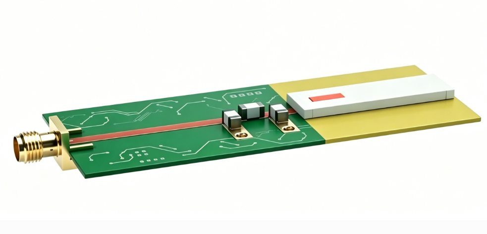
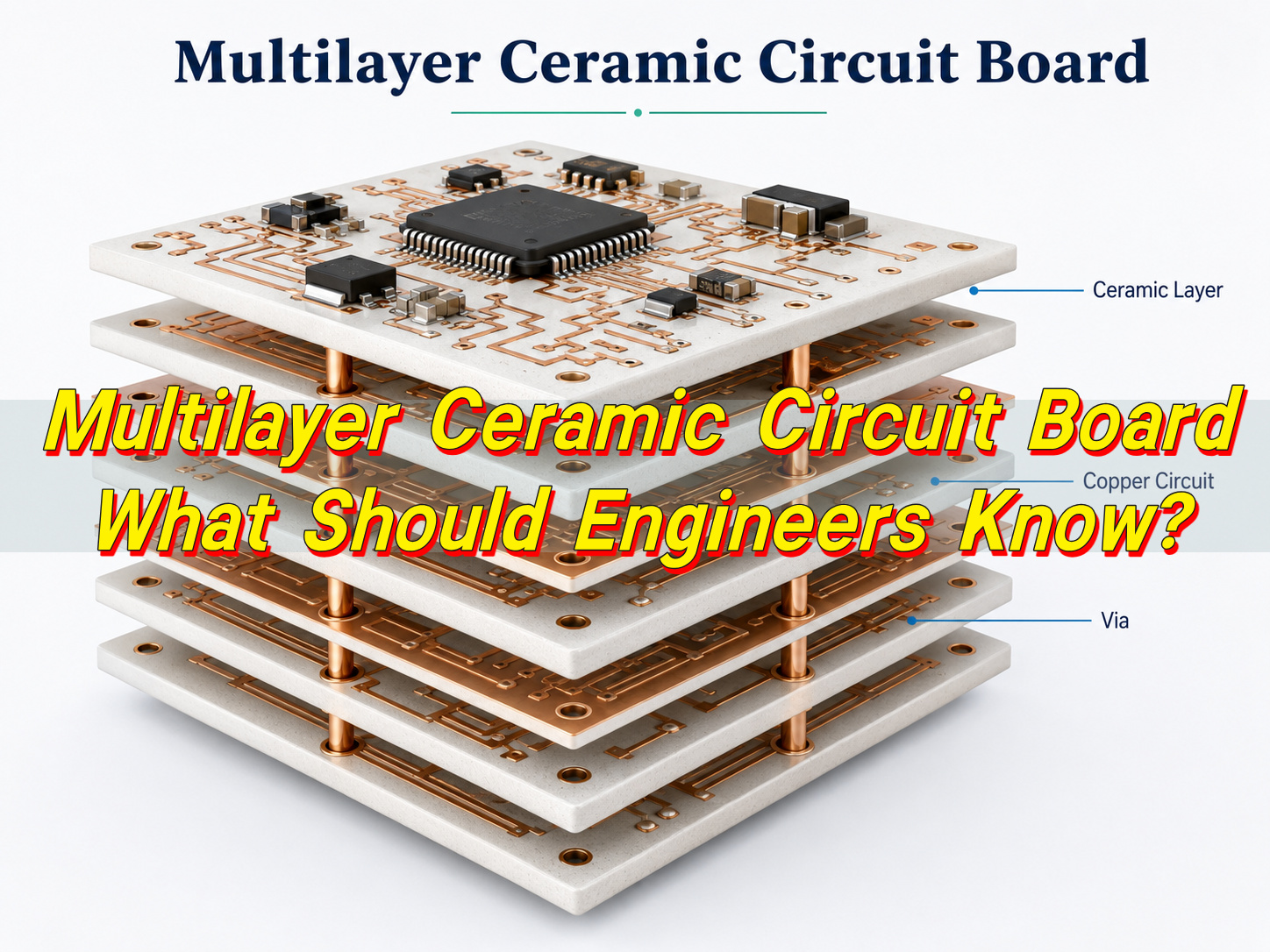
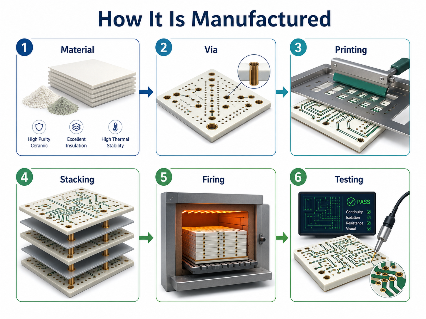
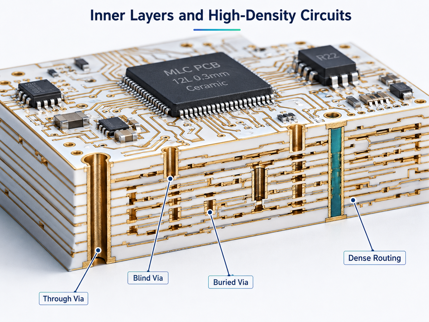
Is RO3010 the right high-frequency material for a compact RF PCB? This guide explains the material in plain language, so you can read the datasheet with more confidence before PCB fabrication.
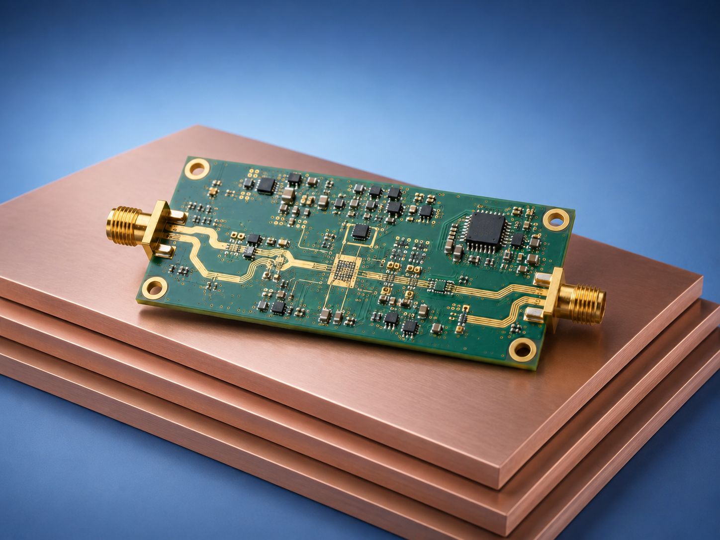
RO3010 is often selected when a circuit needs high dielectric constant, stable RF behavior, and a smaller board area. In this article, we will review its material structure, Dk, thickness, cost factors, applications, and manufacturing support.
What Is Rogers 3010 Material?
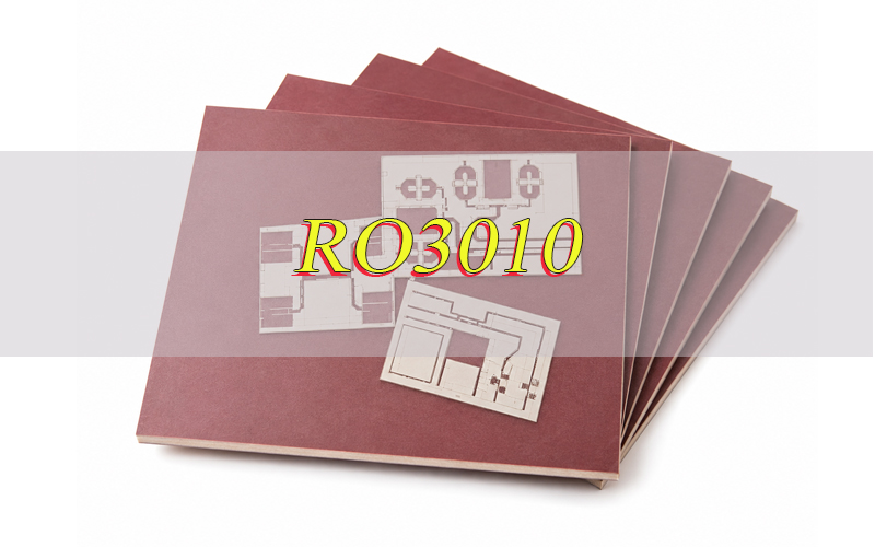
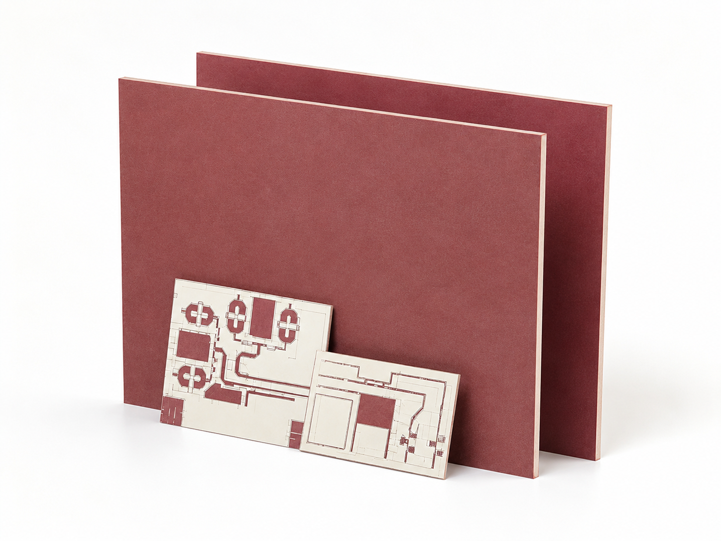
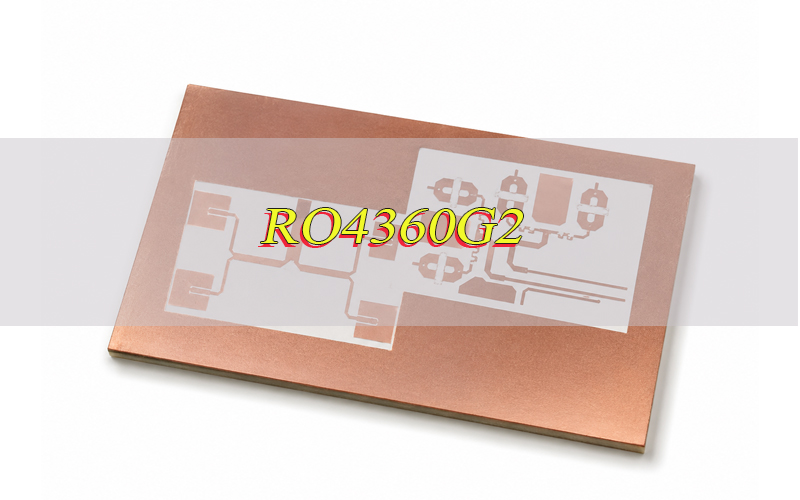
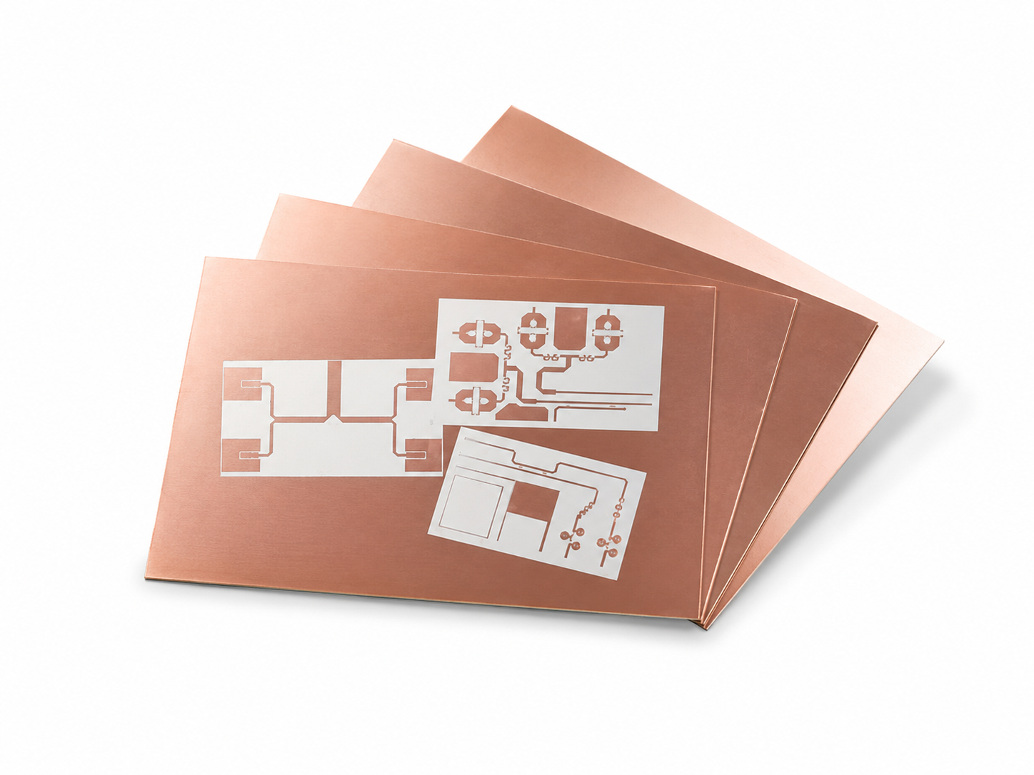
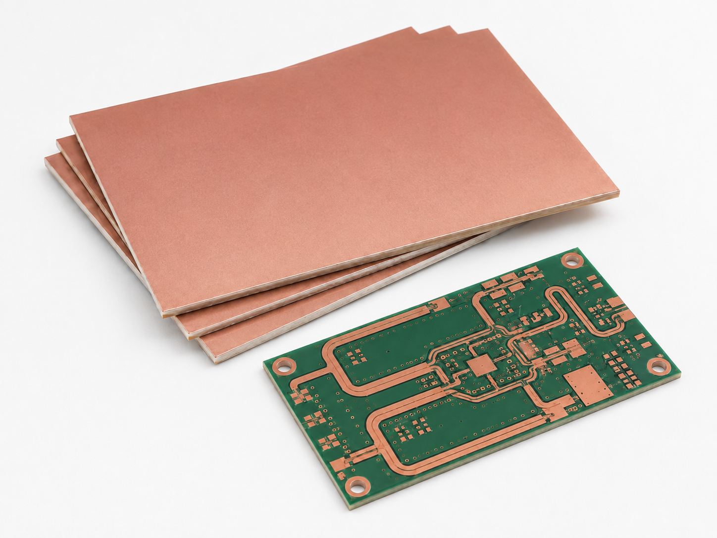
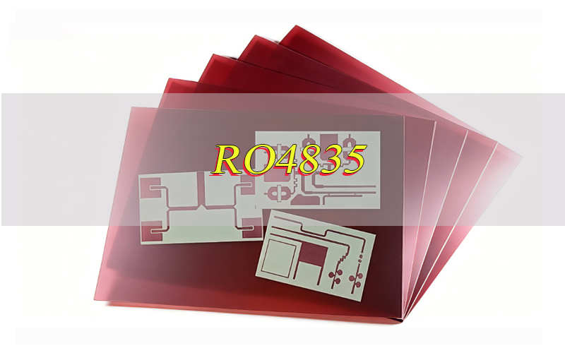
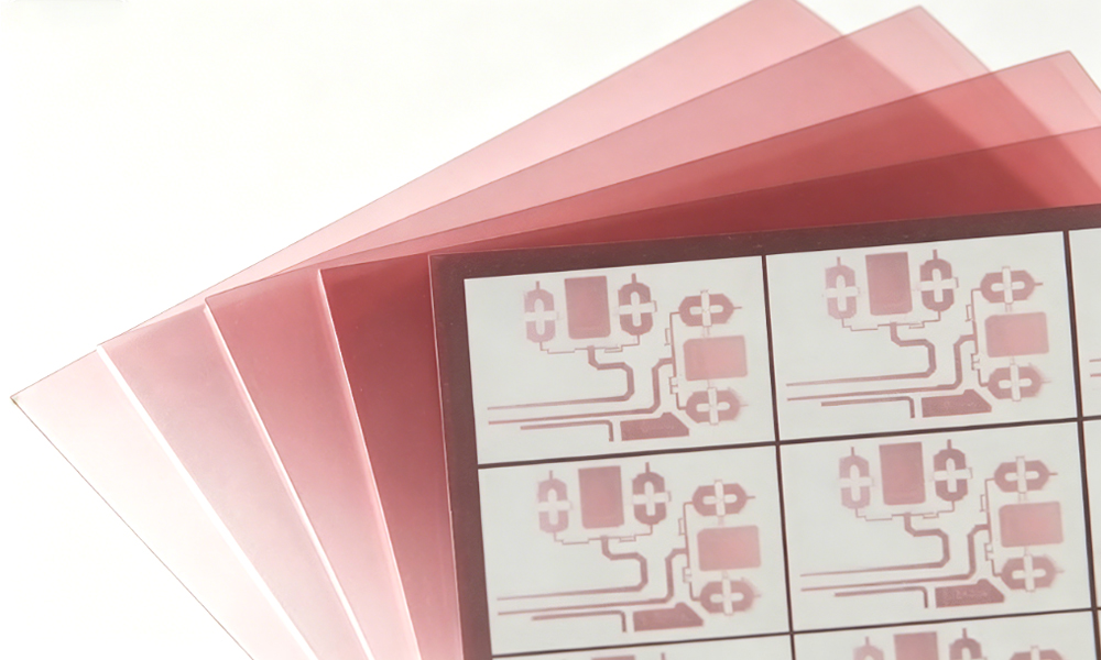
Rogers 3010 material usually refers to Rogers RO3010 laminate. It is a ceramic-filled PTFE composite circuit material designed for high-frequency PCB work. The material belongs to the Rogers RO3000 series, which is widely used for RF and microwave circuits.
In simple terms, it is not standard FR4. FR4 works well for many general electronic boards, while this Rogers material is used when signal stability, dielectric control, and low loss matter more.
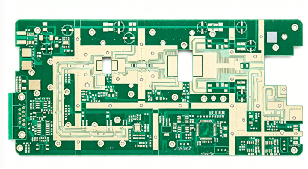
The high dielectric constant helps reduce circuit size. This is useful for compact antennas, filters, RF modules, and microwave layouts where board space is limited.
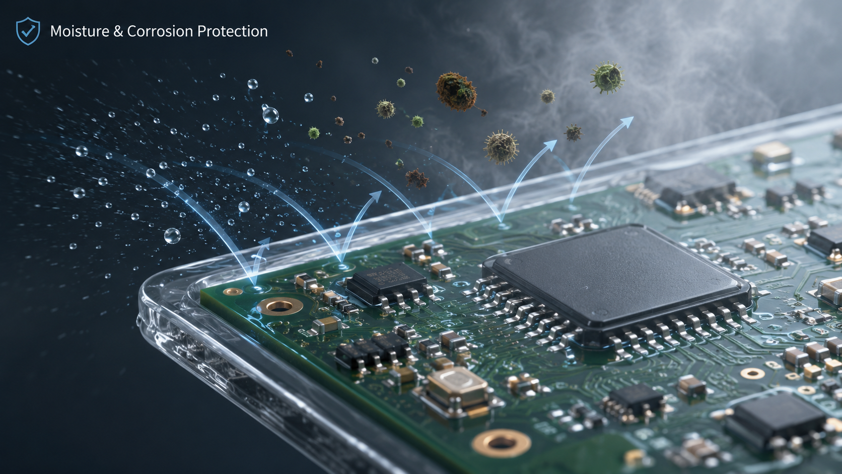
This laminate also has low moisture absorption and controlled thermal expansion. These properties help the PCB keep stable electrical behavior under heat, humidity, and production stress.
Why Choose Rogers RO3010 for High-Frequency PCB Design?
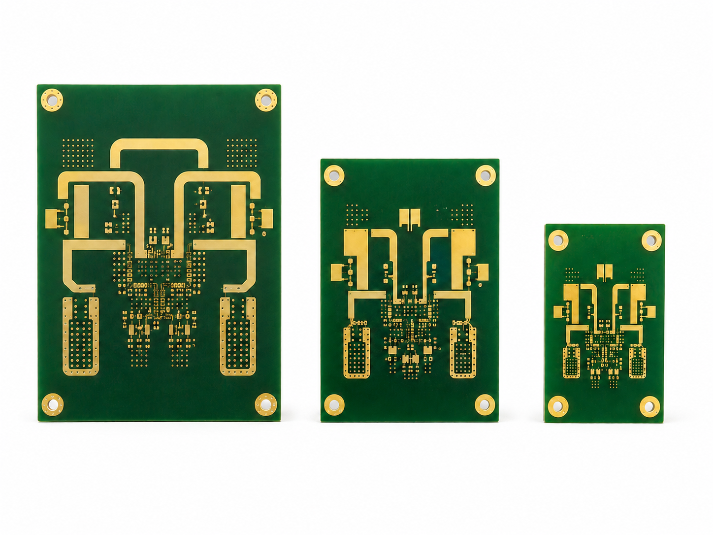
This material is chosen when a PCB needs compact RF layout, stable high-frequency behavior, and better signal control than standard FR4. Its high Dk allows shorter trace structures, while its low loss helps RF signals pass with less energy loss.
High Dk: Supports smaller RF layouts and compact antenna structures.
Low dissipation factor: Helps reduce signal loss at microwave frequency.
Stable CTE: Helps the board remain stable during thermal stress.
Good dimensional stability: Supports tighter line width and spacing control.
Multilayer support: Can support multilayer PCB builds when the stackup is reviewed carefully.
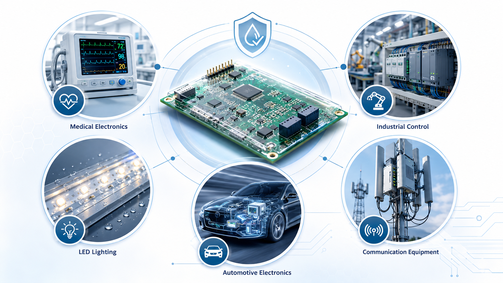
RF application fit: Suitable for RF modules, patch antennas, filters, and communication boards.
How Thick Is the RO3010?
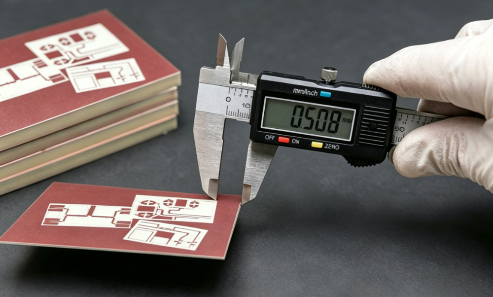
Thestandard laminate thicknesses of RO3010 include 0.005 in, 0.010 in, 0.025 in, and 0.050 in. These are about 0.13 mm, 0.25 mm, 0.64 mm, and 1.28 mm.
The correct thickness depends on the impedance target, copper weight, working frequency, RF trace width, and board stackup. A thinner substrate may suit some high-frequency layouts, while a thicker substrate may fit other impedance or mechanical needs.
Thickness should not be selected only from a catalog. In high-frequency work, even a small thickness change can affect impedance, phase, and antenna behavior.
For PCB fabrication, it is better to send Gerber files, stackup notes, impedance requirements, and copper weight together. This helps the manufacturer review material fit before production.
What Is the Dielectric Constant of RO3010?
RO3010 has a process Dk of 10.20 ± 0.30 at 10 GHz and a design Dk of 11.20. The process Dk helps explain material test data, while the design Dk is more useful for circuit calculation.
This high Dk is the main reason many RF layouts use this substrate. A higher Dk allows the same circuit function to fit into a smaller board area.
Dk also affects impedance, signal velocity, antenna size, and phase behavior. For this reason, the stackup and trace width should be reviewed before fabrication.
Do not treat Dk as a single number without context. Copper thickness, dielectric height, surface finish, etching control, and layout geometry can all change the final PCB result.
Rogers RO3010 Datasheet Overview
The RO3010 datasheet gives the basic material values needed for RF PCB design and fabrication review. And the relevant tables and PDF documents from the Rogers RO3010 datasheet are listed below for your reference.
These values are useful for material review, but final PCB performance still depends on stackup, etching control, lamination, drilling, plating, and inspection.
Rogers RO3010 vs RO3003 vs RO3006: What Is the Difference?
RO3003, RO3006, and RO3010 are ceramic-filled PTFE materials in the same series. The main difference is Dk. Lower Dk gives larger circuit size and often lower loss, while higher Dk supports more compact RF layout.
Item
RO3003
RO3006
RO3010
Material family
RO3000 series
RO3000 series
RO3000 series
Material type
Ceramic-filled PTFE composite
Ceramic-filled PTFE composite
Ceramic-filled PTFE composite
Process Dk
3.00 ± 0.04
6.15 ± 0.15
10.20 ± 0.30
Design Dk
3.16
6.40
11.20
Dissipation factor
0.0010 at 10 GHz
0.0020 at 10 GHz
0.0022 at 10 GHz
Thermal coefficient of Dk
-3 ppm/°C
-262 ppm/°C
-395 ppm/°C
Water absorption
0.04%
0.02%
0.05%
Thermal conductivity
0.50 W/m/K
0.79 W/m/K
0.95 W/m/K
X/Y/Z CTE
17 / 16 / 25 ppm/°C
17 / 17 / 24 ppm/°C
13 / 11 / 16 ppm/°C
Copper peel strength
12.7 lb/in
7.1 lb/in
9.4 lb/in
Density
2.1 g/cm³
2.6 g/cm³
2.8 g/cm³
Flammability rating
UL 94 V-0
UL 94 V-0
UL 94 V-0
Lead-free process compatible
Yes
Yes
Yes
RO3003 is often used when low loss and wider RF structures are preferred. RO3006 sits in the middle. The high-Dk grade in this comparison is more suitable when small circuit size is a major goal.
What Design Factors Affect Rogers RO3010 PCB Performance?
Good material selection is only the first step. The final board result also depends on how the layout and fabrication rules are controlled.
Dielectric thickness: It directly affects impedance and trace size.
Copper weight: It changes trace height, etching behavior, and RF loss.
Trace geometry: RF trace width, spacing, bends, and ground shape need careful control.
Copper roughness: Rough copper can increase conductor loss at high frequency.
Via structure: Via size, stub length, plating, and grounding vias affect RF return path.
Stackup design: Hybrid builds with FR4 or other materials need thermal and mechanical review.
Surface finish: ENIG, immersion silver, or other finishes should match RF needs and assembly flow.
Fabrication tolerance: Line width, spacing, registration, drilling, and plating control all matter.
Testing plan: Electrical test, impedance test, AOI, and visual inspection help confirm build quality.
What Applications Use Rogers RO3010 Substrate?
This substrate is used where high-frequency signals, compact layout, and material stability matter. It appears in antenna systems, communication systems, compact RF modules, and microwave boards.
RF antenna PCB
Patch antenna
GPS antenna board
Microwave circuit board
RF filter board
Satellite communication module
Cellular communication antenna
Broadband RF component
Cable system datalink board
Automotive radar-related RF board
Wireless communication module
High-frequency test board
For many of these uses, standard FR4 may not provide enough Dk stability or low-loss behavior at higher frequency. This high-Dk substrate gives a more suitable base for RF signal control.
How Much Does Rogers RO3010 PCB Material Cost?
The material cost is not a fixed number. The ro3010 price changes with laminate thickness, copper cladding, panel size, stock status, order quantity, and fabrication requirements.
The final PCB price also depends on board size, layer count, hole structure, impedance tolerance, surface finish, testing method, and delivery schedule. A simple 2-layer RF board and a multilayer RF board will not have the same cost level.
Material waste is another factor. If the board outline does not fit the panel size well, usable panel area may drop and cost can rise.
For a more accurate quote, prepare Gerber files, stackup, material thickness, copper weight, surface finish, quantity, and test requirements. These details allow a PCB manufacturer to calculate the cost more clearly.
How Can EBest Circuit Support Rogers RO3010 PCB Manufacturing?
EBest Circuit can support this type of RF PCB project from material review to production-quality fabrication. For RF boards, early technical review helps reduce impedance drift, layout risk, and manufacturing uncertainty before production begins.
Material selection review for Rogers high-frequency laminates
Stackup planning based on frequency, impedance, copper weight, and board thickness
DFM review before fabrication to find spacing, via, copper, and panelization issues
Controlled impedance fabrication for RF traces and transmission lines
Rogers PCB fabrication for prototypes, small batches, and volume production
Surface finish support such as ENIG, immersion silver, and other project-based finishes
AOI, electrical test, visual inspection, and impedance test support
Component sourcing and PCBA assembly for complete electronics manufacturing needs
Production traceability for material batch, process flow, inspection, and shipment records
FAQs About Rogers RO3010 PCB Material
Q1: Is Rogers 3010 the same material as RO3010? A1: Yes. Rogers 3010 usually refers to Rogers RO3010, a ceramic-filled PTFE high-frequency laminate in the RO3000 series. It is mainly used for RF, microwave, antenna, and compact high-frequency PCB designs.
Q2: Which Dk value should be used for RF circuit calculation? A2: For design work, the more useful value is usually the design Dk of 11.20. The material also has a process Dk of 10.20 ± 0.30 at 10 GHz. In practical PCB fabrication, the final impedance result also depends on dielectric thickness, copper weight, trace width, and process tolerance.
Q3: What thicknesses are commonly available for this laminate? A3: Common thicknesses include 0.005 in, 0.010 in, 0.025 in, and 0.050 in, which are about 0.13 mm, 0.25 mm, 0.64 mm, and 1.28 mm. The right thickness should match the target impedance, frequency, copper thickness, and stackup structure.
Q4: Why is this material often used for compact RF circuits? A4: It has a high dielectric constant, so RF structures can be made smaller than many lower-Dk materials. Its design Dk of 11.20 helps reduce circuit size, which is useful for compact antennas, filters, microwave modules, and space-limited RF boards.
Q5: Can it be used for multilayer PCB fabrication? A5: Yes. It can be used in multilayer PCB structures, but the stackup needs careful review. The manufacturer should check bonding material, lamination flow, drilling quality, copper plating, and impedance control before production.
Q6: Is it better than standard FR4? A6: It depends on the application. For general electronic boards, FR4 is still practical and cost-friendly. For high-frequency circuits, this material provides better RF stability because it offers high Dk, low dissipation factor, and more stable high-frequency behavior than standard FR4.
Q7: What mainly affects PCB price for this material? A7: The final price is affected by laminate thickness, copper weight, board size, layer count, impedance tolerance, surface finish, testing requirements, material availability, and lead time. A 2-layer RF board and a complex multilayer RF board will have very different costs.
Q8: What files should be prepared before requesting a quote? A8: For a faster and more accurate quote, prepare Gerber files, stackup details, material thickness, copper weight, surface finish, quantity, impedance requirements, and test requirements. These details help the PCB manufacturer review manufacturability and calculate cost more accurately.
Q9: Can this laminate be combined with FR4 in a hybrid PCB stackup? A9: Yes, hybrid stackups are possible. However, this laminate and FR4 have different material behavior, so the board needs review for thermal expansion, bonding reliability, drilling parameters, registration accuracy, and lamination control.
Q10: When should I choose this material instead of RO3003 or RO3006? A10: Choose it when the design needs higher Dk and smaller RF circuit size. RO3003 is better for lower-Dk, low-loss RF layouts, while RO3006 sits between RO3003 and the high-Dk grade. This material is more suitable for compact RF antennas, filters, and microwave circuit boards.
Conclusion
Rogers RO3010 is a strong choice for high-frequency PCB projects that need high Dk, compact RF layout, stable signal transmission, and precise fabrication control. However, good material alone does not guarantee good board performance. The final result depends on thickness selection, copper weight, stackup design, impedance control, drilling quality, surface finish, and inspection process.
Ready to turn your Rogers RO3010 design into a reliable PCB? Send your Gerber files, stackup details, material thickness, copper weight, impedance requirements, quantity, and delivery needs to sales@bestpcbs.com. EBest Circuit can support your project with DFM review, material selection guidance, controlled impedance PCB fabrication, RF PCB manufacturing, testing, and production traceability. Get a clear quotation and practical manufacturing suggestions before your next build starts.
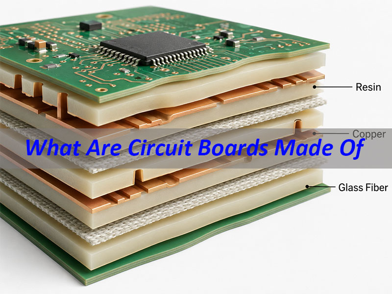
What are circuit boards made of?Circuit boards are made of copper, insulating base materials, resin, glass fiber, solder mask, silkscreen, and surface finishes that work together to carry signals, support components, and protect the circuit. This article explains the main PCB materials, how they affect board performance, and how to choose the right material for different applications.
Choosing the right circuit board material is also the first step toward reliable PCB and PCBA production. At EBest Circuit, we help customers review PCB materials, stackup, copper thickness, surface finish, DFM risks, component sourcing, assembly process, and testing needs before production starts. If you want a board that matches your electrical, thermal, and assembly requirements, pls feel free to send your Gerber files and project details to sales@bestpcbs.com for engineering support.
What Are Circuit Boards Made Of?
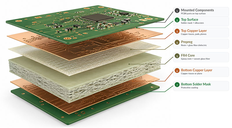
What are circuit boards made of? Most circuit boards use an insulating base, copper, resin, glass fiber, solder mask, silkscreen ink, and surface finish. These materials work together to support components, carry signals, control heat, and protect the circuit.
For many standard PCBs, the main base material is FR4. FR4 combines woven glass fiber with epoxy resin. This structure gives the board strength, insulation, and stable performance.
However, not every PCB uses the same material. A simple consumer PCB may use standard FR4. A high frequency board may need Rogers or PTFE based material. A power LED board may need an aluminum or copper core. Therefore, the right material depends on the final application.
In simple terms, a circuit board is not made from one material. It is a layered structure. Each layer has a clear job.
Core PCB Raw Materials
A printed circuit board usually contains several main raw materials. Each one affects performance, cost, and reliability.
Copper gives the PCB its electrical path. Resin and glass fiber form the base structure. Meanwhile, solder mask protects the copper pattern during soldering and long term use.
Also, surface finish matters. It keeps copper pads from oxidizing and helps components solder well during PCBA assembly.
How Copper, Resin, and Glass Work Together
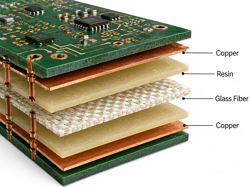
Copper, resin, and glass fiber form the heart of many circuit boards.
Copper carries current and signals.
PCB manufacturers laminate copper foil onto the base material. Then they etch it into traces, pads, and copper planes. In multilayer boards, copper also forms power layers, ground layers, and signal layers.
Resin bonds and insulates the board.
Resin holds the glass cloth and copper structure together. It also insulates different copper layers. Because of this, resin quality affects heat resistance, moisture resistance, and electrical reliability.
Glass fiber adds mechanical strength.
Glass cloth helps the board stay flat and stable. It also reduces warpage during fabrication and soldering. As a result, the PCB can handle drilling, plating, routing, and assembly more reliably.
Together, these three materials decide many PCB properties. For example, they affect board thickness, impedance, thermal expansion, and long term durability.
PCB Laminate and Prepreg
PCB laminate is the base sheet used to make a circuit board. A common laminate is copper clad FR4. It includes copper foil, epoxy resin, and glass cloth.
Laminate quality directly affects the final PCB. It can influence heat resistance, drilling quality, copper adhesion, impedance control, and dimensional stability.
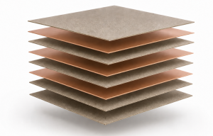
For multilayer PCBs, manufacturers also use prepreg. Prepreg is glass cloth soaked with semi cured resin. During lamination, heat and pressure make the resin flow. Then it bonds the PCB layers together.
Prepreg is important because it controls:
Layer bonding strength
Dielectric spacing
Final board thickness
Impedance stability
Resin flow around copper
Multilayer reliability
Therefore, prepreg is not just “glue.” It is a key dielectric material in multilayer PCB stackups.
Common PCB Material Types
Different products need different PCB materials. The table below shows common options.
PCB Material
Common Use
Main Benefit
Standard FR4
Consumer electronics, control boards
Good cost and balanced performance
High Tg FR4
Automotive, industrial, lead free assembly
Better heat resistance
Polyimide
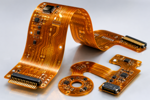
Flexible PCB, rigid flex PCB
Flexible and heat stable
PTFE / Rogers
RF, microwave, antenna PCB
Low signal loss
Aluminum Core PCB
LED lighting, power modules
Better heat dissipation
Copper Core PCB
High power LED, automotive lighting
Strong thermal spreading
Ceramic PCB
Power electronics, harsh environments
High thermal conductivity
FR4 works well for many standard products. However, high power, high speed, or high temperature designs often need better material.
For example, RF circuits need stable Dk and low Df. LED boards need strong heat dissipation. Flexible electronics need polyimide. Therefore, material choice should follow the product function, not only the price.
Key PCB Material Properties
When engineers choose PCB materials, they often review several key properties.
Tg: Glass Transition Temperature Tg shows when the material starts to soften. A higher Tg helps the board handle heat during lead free soldering and operation.
Td: Decomposition Temperature Td shows when the material starts to break down. Higher Td gives better thermal safety.
CTE: Coefficient of Thermal Expansion CTE shows how much the material expands when temperature changes. Lower and stable CTE helps protect plated holes and multilayer structures.
Dk: Dielectric Constant Dk affects signal speed and impedance. High speed and RF boards need controlled Dk values.
Df: Dissipation Factor Df affects signal loss. Lower Df helps high frequency signals travel with less loss.
Copper Thickness Copper thickness affects current capacity and heat. Power boards often need thicker copper, while fine line boards may need thinner copper for accurate etching.
Peel Strength Peel strength shows how well copper bonds to the base material. Good peel strength helps prevent copper lifting during soldering and use.
These properties help engineers avoid material mismatch. In addition, they help manufacturers control reliability before production starts.
What Are Green Circuit Boards Made Of?
Green circuit boards are not green because of the base material. The green color usually comes from green solder mask.
Solder mask covers most copper areas on the PCB. It protects copper from oxidation, dust, moisture, and solder bridging. It also gives the board a cleaner surface for assembly and inspection.
Although green is the most common color, PCB solder mask can also be black, blue, red, white, yellow, or matte colors. However, the color does not always show the base material. A green PCB may still use FR4, high Tg FR4, polyimide, or another substrate.
So, when customers ask what green circuit boards are made of, the answer is simple: the green layer is solder mask, while the main board structure usually includes copper, resin, and glass fiber.
How to Choose Circuit Board Material
Choosing the right circuit board material starts with the product requirement. Cost matters, but function comes first.
Before selecting a PCB material, engineers should check:
Operating temperature
Board thickness
Copper thickness
Current load
Signal speed
Frequency range
Heat dissipation needs
Flexibility requirements
Assembly process
Reliability standard
Production quantity
For standard electronics, FR4 often works well. For higher heat, high Tg FR4 is safer. For RF and microwave circuit boards, low loss materials may be necessary. For LED and power boards, aluminum core, copper core, or ceramic materials can improve heat transfer.
Also, do not choose material only by datasheet values. The PCB stackup, copper design, drilling process, surface finish, and assembly process also affect final performance.
A professional PCB manufacturer can help review the stackup, impedance, copper weight, base material, surface finish, and DFM risks before fabrication. This step saves time and reduces production problems.
FAQs About What Circuit Boards Are Made Of
Q1: What are printed circuit boards made of? A1: Printed circuit boards are usually made of base substrate, copper foil, resin, glass fiber, solder mask, silkscreen, and surface finish. Standard rigid PCBs often use FR4.
Q2: What are PCB boards made of? A2: PCB boards use insulating materials and conductive copper layers. The insulating material may be FR4, high Tg FR4, polyimide, PTFE, ceramic, aluminum core, or copper core material.
Q3: What are circuit board traces made of? A3: Circuit board traces are made of copper. These copper paths connect components and carry signals or power across the PCB.
Q4: What plastic are circuit boards made of? A4: Most circuit boards are not made of ordinary plastic. Many standard PCBs use glass fiber reinforced epoxy resin, also called FR4.
Q5: What are circuit board pins made of? A5: Circuit board pins usually come from connectors or components. They often use copper alloy with tin, nickel, or gold plating.
Q6: Are all circuit boards made from FR4? A6: No. FR4 is common, but not universal. High frequency boards may use Rogers or PTFE materials. LED boards may use metal core materials. Flexible boards often use polyimide.
Q7: What are cell phone circuit boards made of? A7: Cell phone PCBs often use thin multilayer materials, fine copper traces, flexible polyimide circuits, and high density interconnect structures.
Q8: Why does PCB material selection matter? A8: PCB material affects heat resistance, signal quality, soldering stability, mechanical strength, and long term reliability. Good material selection helps reduce production risk.
In conclusion, circuit boards are made from several materials, not one simple substance. Copper creates the electrical paths. Resin and glass fiber build the base structure. Laminate and prepreg form the PCB stackup. Solder mask, silkscreen, and surface finish protect the board and support assembly.
For simple products, standard FR4 may be enough. However, high speed, high power, RF, medical, automotive, and industrial products often need more careful material selection.
Need help choosing the right PCB material? Send your Gerber files, stackup, BOM, and application details to EBest Circuit. Our team can support PCB material review, DFM analysis, PCB fabrication, component sourcing, PCBA assembly, testing, and turnkey production. Pls feel free to contact us at sales@bestpcbs.com for a quotation.
Are you choosing S1150G for a halogen-free Tg150 FR4 PCB material but still unsure about its Tg value, datasheet properties, and real PCB applications? Shengyi S1150G is a practical mid-Tg FR4 material for projects that require halogen-free performance, lead-free process compatibility, and stable PCB fabrication.
This guide explains what this material is, how to read its datasheet, why Tg150, Tg155, and Tg160 may appear in different material references, whether HF means high-frequency, and how this laminate compares with standard FR4. It also shows where this material is commonly used and how EBest can support PCB fabrication from material review to finished board delivery.
What Is Shengyi S1150G PCB Material?
Shengyi S1150Gis a halogen-free, lead-free compatible FR4 PCB material from Shengyi Technology. It belongs to the rigid PCB material family and is commonly used when a project needs a practical balance of cost, thermal stability, and environmental compliance.
It is often described as a mid-Tg FR4 material. Its material data lists it as a halogen-free, mid-Tg material with Tg 155°C, Td 355°C, and Z-axis expansion of 2.8%.
Compared with common FR4, this laminate is a better fit for designs that need halogen-free material documentation and lead-free process compatibility. It is widely used in rigid PCB designs, including consumer electronics, LED electronics, automotive electronics, and communication equipment.
In PCB fabrication, the material should be checked together with the full board requirement. Board thickness, copper thickness, layer count, surface finish, soldering profile, and quality standards all affect the final result.
Features of S1150G Halogen-Free Tg150 FR4 PCB Material
This laminate is a useful choice for projects that need halogen-free FR4 with mid-Tg thermal performance. It supports common PCB production processes and fits many electronic products that need lead-free assembly compatibility.
Halogen-free material system The material is described as free of halogen, antimony, and red phosphorus. This helps support halogen-free PCB requirements and cleaner material documentation.
Mid-Tg FR4 performance The material is often searched as S1150G Tg 150, but its data lists Tg as 155°C by DSC.
Lead-free process compatibility This FR4 grade is positioned as a lead-free compatible material, making it suitable for many modern PCB and PCBA production flows.
Good mechanical processability It supports standard PCB drilling, routing, lamination, and finishing processes.
Thermal resistance for common PCB needs Its data lists Td as 355°C, T260 as 60 minutes, and T288 as 45 minutes. These values support many lead-free PCB applications.
UL94 V-0 flame rating Its material data lists flammability as V-0 under UL94 conditions.
Shengyi S1150G Datasheet Overview
The S1150G datasheet provides main thermal, electrical, and mechanical values for PCB material review. The table below lists common material data. Attached is a download link for Shengyi S1150G datasheet:
The CTI value of Shengyi S1150G PCB laminate is no less than 600V and falls under Class 0 insulation grade. Its exceptional dielectric safety lays solid foundation for long-term stable operation in demanding electronic devices.
Class 0 qualification fully complies with stringent global safety standards, offering strong resistance against electric tracking under continuous high-voltage working conditions.
This high-performance substrate is widely deployed in high-voltage application areas, including industrial control systems, automotive electronics and primary power circuit designs.
It combines superior comparative tracking performance, remarkable CAF resistance and halogen-free material formula, balancing reliable operational capability and environmental compliance requirements.
What Is the Tg Value of Shengyi S1150G? Tg150, Tg155, or Tg160?
The practical answer is: Shengyi S1150G is commonly treated as a Tg150-class FR4 material, while its material data lists Tg as 155°C by DSC. This is why many people search for S1150G Tg 150 or Tg150 FR4.
The terms Tg150 and Tg155 are often used in the market to describe the same general material class. In formal material review, the exact test method matters. The Tg value is commonly listed as 155°C by DSC.
You may also see Tg160 in some material listings. This usually comes from a different test method, such as DMA, while DSC data may still show 155°C. The difference is related to test method rather than a simple material conflict.
For clearer documentation, it is better to write Shengyi S1150G or equivalent halogen-free FR4, Tg 155°C by DSC. This wording helps the PCB factory confirm the correct laminate and prepreg before production.
Is S1150G HF a High-Frequency Material?
No. S1150G HF is not a dedicated high-frequency PCB material. In PCB material naming, HF is often used to describe halogen-free laminates. For this laminate, that meaning is more accurate than treating it as an RF or microwave-grade material.
The material has Dk around 4.5 at 1GHz and Df around 0.011 at 1GHz. These values can support many standard FR4 PCB products, such as control boards, LED boards, automotive electronics, and general communication boards.
For RF antenna, radar, microwave, or very low-loss transmission applications, a dedicated RF laminate is usually a better choice. This product should be viewed as a halogen-free FR4 material with stable general-purpose PCB performance.
What Applications Use Shengyi S1150G PCB Material?
S1150G PCB material is used in many rigid PCB applications where halogen-free FR4, mid-Tg performance, and lead-free process compatibility are required. Typical application areas include consumer electronics, LED products, automotive electronics, communication equipment, and industrial control boards.
Consumer electronics PCB: Tablets, notebooks, smart devices, and other compact electronic products.
LED control PCB: LED drivers, lighting control boards, and lighting-related electronic assemblies.
Automotive electronics PCB: Selected automotive control boards and electronic modules after project review.
Communication equipment PCB: General communication products where dedicated low-loss RF material is not required.
Industrial control PCB: Control modules, interface boards, power management boards, and automation-related products.
Multilayer halogen-free PCB: Multilayer PCB fabrication when the stackup, prepreg, copper balance, and pressing process are properly controlled.
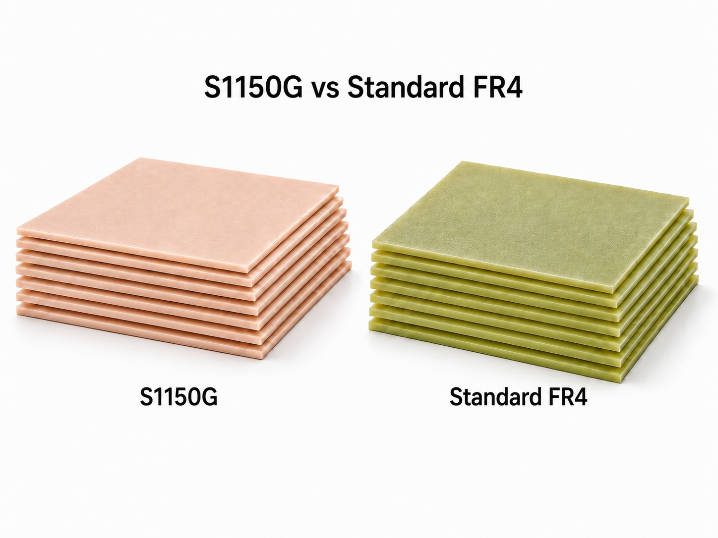
S1150G vs Standard FR4: What Is the Difference?
This material belongs to the FR4 family, but it offers a more specific material position than common FR4. Its value comes from halogen-free chemistry, mid-Tg performance, and lead-free process compatibility.
Item
Shengyi S1150G FR4
Standard FR4
Material type
Halogen-free mid-Tg FR4.1
General FR4 material family
Halogen-free status
Yes
Depends on selected grade
Tg value
155°C by DSC
Commonly varies by grade
Td value
355°C
Varies by grade
Lead-free process
Compatible
Must be confirmed
Dk / Df
Dk 4.5 and Df 0.011 at 1GHz
Varies by material system
Environmental positioning
Better fit for halogen-free requirements
Depends on material choice
Typical applications
Consumer, LED, industrial, automotive, communication PCB
General PCB production
Cost level
Usually higher than basic FR4
Usually lower
Best fit
Projects needing halogen-free FR4 and mid-Tg performance
Cost-sensitive common PCB projects
For projects with clear halogen-free requirements, FR4 S1150G is often a better fit than basic FR4. For simple boards without environmental material requirements, standard FR4 may still be enough.
How Does EBest Support S1150G PCB Fabrication?
EBest provides practical support for S1150G PCB fabrication, from material review to finished board delivery. Our goal is to help each project use the right material, reduce fabrication risk, and move smoothly from prototype to production.
Material review: We can check whether Shengyi S1150G matches the drawing requirement, Tg note, halogen-free requirement, lead-free process, board structure, and production target.
FreeDFM review before fabrication: Our team reviews Gerber files, drill files, copper spacing, annular rings, solder mask clearance, routing design, panelization, and special fabrication notes before production starts.
Multilayer stackup support: For multilayer boards, we can help review layer structure, laminate and prepreg matching, copper balance, dielectric thickness, impedance needs, and lamination feasibility.
PCB fabrication from prototype to batch production: EBest supports prototype, small batch, and mass production, helping projects keep material choice, process control, and quality standards consistent.
Controlled PCB manufacturing process: We support drilling, copper plating, solder mask, surface finish, routing, electrical testing, and final inspection with process control suitable for halogen-free FR4 boards.
PCBA assembly and component sourcing: Beyond bare board fabrication, EBest can also provide component sourcing, SMT assembly, through-hole assembly, functional testing, and turnkey PCBA support.
Quality inspection and testing: Our quality process can include incoming material checks, AOI, electrical testing, impedance testing when required, X-ray inspection for assembled boards, and final quality inspection.
Traceability and production support: For industrial control, communication, automotive electronics, LED, and medical-related PCB projects, EBest can support production traceability and stable delivery from trial build to repeat orders.
One-stop technical response: If your drawing only says S1150G material or S1150G FR4, EBest can help confirm whether additional details are needed, such as Tg method, copper thickness, surface finish, soldering process, and environmental documentation.
FAQs About Shengyi S1150G
Q1: Why is this laminate often selected for halogen-free PCB projects? A1: It offers halogen-free chemistry, mid-Tg performance, and lead-free process compatibility. It is a practical FR4 choice for rigid PCBs that need cleaner material documentation and stable production performance.
Q2: Why do some drawings or searches call it S1150G Tg150? A2: This material is often grouped into the Tg150-class FR4 category in the market. Its Tg is commonly listed as 155°C by DSC, while some references may show 160°C by DMA because of different test methods.
Q3: Which data matters when comparing this material with other FR4 materials? A3: Useful data includes Tg, Td, T260, T288, Z-axis expansion, Dk, Df, water absorption, flame rating, and material compliance. These values help judge whether the laminate fits the product requirement.
Q4: Can this material support lead-free assembly? A4: Yes. It is positioned as lead-free compatible FR4. The final result still depends on PCB thickness, copper design, moisture control, surface finish, and reflow conditions.
Q5: What file details help speed up an S1150G PCB quotation? A5: Gerber files, stackup, finished board thickness, copper thickness, quantity, surface finish, solder mask color, impedance needs, assembly requirement, and any material certificates should be provided.
Q6: When should another material be considered instead of this laminate? A6: Another material may be needed if the design requires lower dielectric loss, RF or microwave performance, higher Tg, special thermal conductivity, confirmed CTI grade, or project-specific approval.
Q7: What services can EBest provide for an S1150G PCB project? A7: EBest can support PCB fabrication(including FR4 PCB, MCPCB, Ceramic PCB and so on), DFM review, multilayer PCB production, component sourcing, PCBA assembly, testing, and prototype-to-production support.
Get a Fast Quote for S1150G PCB
Looking for a reliable S1150G PCB fabrication partner for prototype, small batch, or production? Send us your Gerber files, stackup, board thickness, copper thickness, quantity, surface finish, and assembly requirements. EBest will review the material callout, check manufacturability, and provide a fast quotation with practical suggestions for PCB fabrication and assembly.
For faster support, email us at sales@bestpcbs.com. Our team will review your S1150G PCB requirements and help you move from material confirmation to finished board delivery with clear technical support and stable production control.
What is IPC 4101, and why does it matter when a PCB stackup uses S1170G or another high Tg FR4 laminate? PCB material selection is not only about writing “FR4” on a fabrication drawing. A stable board depends on laminate type, prepreg, copper foil, Tg, CTE, resin system, glass style, board thickness, and thickness tolerance.
For example, when S1170G is reviewed for a high Tg FR4 PCB, the material data sheet should be read together with the related IPC 4101 requirement, stackup design, copper weight, and soldering profile.
This article explains IPC-4101 in a practical way. It covers the standard meaning, latest revision, material coverage, thickness tolerance, specification overview, slash sheet use, IPC-4101 vs IPC-4103, official PDF access, and common FAQ topics.
What Is IPC 4101?
IPC 4101 is a specification for base materials used in rigid and multilayer printed boards. The IPC-4101E-WAM1 table of contents states that this specification covers base materials called laminate or prepreg, used mainly for rigid or multilayer printed boards for electrical and electronic circuits.
In simple terms, IPC-4101 helps define what PCB laminate and prepreg should meet before they are used in production. It gives a shared material language for PCB designers, PCB factories, laminate suppliers, purchasing teams, and quality teams.
IPC-4101 is not the same as a complete finished PCB acceptance standard. It focuses on base materials, material callouts, laminate and prepreg classification, test references, thickness rules, cladding details, surface quality, and slash sheets.
For PCB projects, IPC 4101 is often used when a drawing must define material requirements more clearly than “FR4.” This matters for high Tg PCB, lead free assembly, multilayer PCB, controlled impedance PCB, industrial PCB, automotive PCB, and medical electronics PCB.
What Is the Current Version of IPC 4101?
The current IPC store listing shows IPC-4101E-WAM1 as the recent revision with Amendment 1. Public standards-store information states that IPC-4101E-WAM1 contains 70 individual specification sheets and covers laminate or prepreg materials listed after the main body of the standard.
IPC-4101E-WAM1 was published in April 2020, according to the public table of contents. This version follows earlier IPC 4101 B, IPC 4101 C, IPC 4101 D, and IPC 4101 E releases.
Older drawings may still mention IPC 4101 B, IPC 4101 C, or IPC 4101 E. That does not always mean the drawing should be changed automatically. Some long life products may need to keep the exact revision written in the approved drawing package.
For a new PCB build, the safer approach is to check the drawing note, purchase requirement, approved material list, and official IPC store page. If no revision is stated, confirm the required IPC-4101 version before production release.
What Materials Are Used in IPC 4101?
IPC 4101 covers PCB base materials, mainly laminate and prepreg for rigid and multilayer printed boards. These materials form the dielectric and bonding structure of the PCB, so they affect thermal resistance, dimensional behavior, copper bonding, and long term reliability.
Common material categories include:
Laminate materials used as rigid PCB cores.
Prepreg materials used as bonding layers in multilayer PCB lamination.
Clad laminate with copper foil bonded to one or both sides.
Unclad laminate used where copper foil is not part of the base material.
Glass reinforced epoxy systems often associated with FR4 style PCB materials.
High Tg FR4 systems for higher thermal demand and lead free soldering.
Polyimide materials for higher thermal resistance applications.
Cyanate ester materials for selected high performance PCB applications.
High speed or low loss materials when matched to the relevant slash sheet and material data sheet.
Copper foil cladding defined by type, nominal weight, or thickness.
The IPC-4101 callout structure includes material designator, specification sheet number, nominal laminate thickness, metal cladding type and weight or thickness, thickness tolerance class, and surface quality class.
What Are IPC 4101 Thickness Tolerance Requirements?
The IPC-4101E table of contents states that nominal laminate thickness is identified by four digits. For metric specification, 1500 means 1.5 mm. For Imperial units, the four digits indicate thickness in ten thousandths of an inch. Here are important thickness points:
State whether thickness is measured over copper or over dielectric.
Use the nominal laminate thickness code in the material callout.
Add the required thickness tolerance class.
Do not rely only on the phrase “standard tolerance.”
Check copper foil because copper weight changes final board thickness.
Review stackup thickness after lamination, especially for multilayer PCB.
For impedance control, review dielectric thickness, Dk, copper profile, and etching compensation.
For high Tg PCB, confirm that thermal performance and thickness control both match the production need.
For strict projects, the PCB drawing should state finished board thickness, tolerance, copper weight, stackup, controlled impedance data, laminate slash sheet, and acceptable material names.
What Does the IPC 4101 Specification Cover?
IPC 4101 should be read as a material control system rather than a simple material list. It uses a main standard plus slash sheets to describe laminate and prepreg requirements for different base material grades.
Item
Specification
Standard Name
Specification for Base Materials for Rigid and Multilayer Printed Boards
Paid standard from IPC official store or authorized standards seller
The public table of contents is useful for understanding structure, but it is not the full paid IPC 4101 PDF. For formal production, drawing approval, or audit records, use the official paid document.
How to Use IPC-4101 Slash Sheets for PCB Material Selection?
IPC-4101 slash sheets help PCB manufacturers match laminate and prepreg materials with specific performance requirements. When a drawing lists IPC-4101/99, IPC-4101/40, IPC-4101/98, or IPC-4101/126, the slash number points to a defined material category inside the IPC-4101 standard.
A slash sheet is not a single material brand. It is a material classification that must be checked together with the laminate supplier’s datasheet.
The chart below shows common IPC-4101 slash sheet search terms and public model references. It can help readers understand how slash sheets relate to real PCB laminate families, but it should not replace the official IPC document.
Search Term / Slash Sheet
Public Model Reference
Nominal Dk Shown
Material Description
IPC-4101E/29
N4000-13, N4000-13SI, N4103-13, N4203-13
3.60, 3.20
High speed, low loss, modified epoxy, flame rating 94 V-0
IPC-4101E/30
N5000, N5105, N5205, N5305
3.60
BT epoxy, flame rating 94 V-0
IPC 4101 40 / IPC-4101E/40
N7000-2HT, N7105-2 HT, N7205-2 HT
3.50
Non-MDA toughened polyimide, flame rating 94 V-0
IPC 4101 41 / IPC-4101E/41
N7000-3, N7105-3, N7205-3, N7305-3
3.50
Non-MDA toughened polyimide, flame rating 94 V-1
IPC-4101E/42
N7000-3F, N7105-3F, N7205-3F, N7305-3F
4.00
Non-MDA toughened and filled polyimide, flame rating 94 V-1
IPC 4101 98 / IPC-4101E/98
N4000-29, N4000-29NF, N4105-29, N4205-29
4.30
High Tg multifunctional epoxy, flame rating 94 V-0
IPC 4101 99 / IPC-4101E/99
N4000-29, N4105-29, N4205-29
4.30
Lead free, high Tg multifunctional epoxy, flame rating 94 V-0
Very to extreme low loss PPE systems, flame rating 94 V-0
IPC-4101E/126
N4000-29, N4105-29, N4205-29
4.30
Lead free, high Tg multifunctional epoxy, flame rating 94 V-0
IPC-4101E/129
N4000-29, N4105-29, N4205-29
4.30
Lead free, high Tg multifunctional epoxy, flame rating 94 V-0
The AGC reference guide maps selected IPC-4101E slash sheets to public model references, nominal Dk values, and material descriptions. For example, IPC-4101E/126 and IPC-4101E/129 are shown with N4000-29, N4105-29, and N4205-29 references, nominal Dk 4.30, and a lead free high Tg multifunctional epoxy description.
For terms such as IPC 4101 21, IPC 4101 24, and IPC 4101 26, the exact material category should be confirmed in the official IPC-4101 PDF. Public material charts may not include every slash sheet.
Before approving a laminate, check the slash sheet together with Tg, CTE, Dk, Df, copper foil, thickness tolerance, flame rating, lead free soldering compatibility, and the approved material list.
What Is the Difference Between IPC-4101 and IPC-4103?
IPC-4101 and IPC-4103 both relate to PCB base materials, but their main use is different. IPC-4101 covers laminate and prepreg for rigid and multilayer printed boards, while IPC-4103 covers base materials for high speed and high frequency applications.
IPC-4103B covers high speed and high frequency performance plastic substrates used for printed boards for microstrip, stripline, high speed digital, and high frequency circuits. It also states that laminates controlled by this specification usually have a dissipation factor of less than 0.005 as a general guideline.
Item
IPC-4101
IPC-4103
Official Title
Specification for Base Materials for Rigid and Multilayer Printed Boards
Specification for Base Materials for High Speed/High Frequency Applications
Main Material Type
Laminate and prepreg
High speed and high frequency plastic substrates
Main PCB Use
Rigid and multilayer printed boards
Microstrip, stripline, high speed digital, and high frequency circuits
Current Public Revision
IPC-4101E-WAM1
IPC-4103B
Published Date Shown
April 2020
November 2017
Main Focus
Material grade, slash sheets, laminate thickness, cladding, and surface quality
High speed and high frequency material behavior
Typical Selection Need
FR4, high Tg FR4, polyimide, multilayer PCB base material control
RF PCB, high speed digital PCB, and microwave related material control
In practical PCB sourcing, IPC-4101 is used more often for general rigid and multilayer PCB base materials. IPC-4103 is more suitable when the circuit depends strongly on controlled Dk, Df, and high frequency behavior.
Where Can You Get the Official IPC-4101 PDF File?
The full IPC 4101 PDF is a paid standards document. Use the official IPC store or an authorized standards store rather than unofficial file sharing pages.
You can access it from or directly download via the following PDF file link:
IPC official store: use the IPC-4101E-WAM1 listing for Revision E with Amendment 1.
IPC public table of contents: use it to understand the scope, classification system, callout examples, nominal thickness method, and slash sheet structure. It is not the complete standard.
Authorized standards sellers: verify revision, language, license type, and PDF access terms before purchase.
Avoid unofficial “free IPC 4101 PDF” pages. They may be outdated, incomplete, or unauthorized, which can create confusion during material approval and quality review.
FAQs About IPC-4101
Q1: What document from the IPC 4101 standards will be used by a board fabricator to identify compatible materials for a PCB stackup?
A1: The fabricator will use the IPC-4101 slash sheets, the PCB drawing, stackup, approved material list, laminate supplier data sheet, and purchasing notes. Each specification sheet outlines requirements for laminate and prepreg for a product grade.
Q2: What does IPC 4101/121 Tg mean?
A2: It usually refers to the glass transition temperature requirement related to IPC-4101 slash sheet 121. The exact Tg value should be checked in the official IPC 4101 PDF and compared with the laminate supplier data sheet before approval.
Q3: What is IPC 4101/126 material?
A3: IPC 4101/126 material refers to a slash sheet material category under IPC-4101. A public AGC reference maps IPC-4101E/126 to N4000-29, N4105-29, and N4205-29, with nominal Dk 4.30 and a lead free high Tg multifunctional epoxy description.
Q4: What does IPC 4101/129 refer to?
A4: IPC 4101/129 is another IPC-4101 slash sheet reference. In the AGC public chart, IPC-4101E/129 is grouped with IPC-4101E/126 for N4000-29 related laminate and prepreg references.
Q5: What is IPC 4101 40?
A5: IPC 4101 40 is commonly used as a search form for IPC-4101/40. The AGC reference chart lists IPC-4101E/40 with N7000-2HT, N7105-2 HT, and N7205-2 HT, with a non-MDA toughened polyimide description.
Q6: What should be checked in IPC 4101/126 specification details?
A6: Check the official slash sheet, supplier data sheet, resin system, reinforcement, Tg, CTE, Dk, Df, copper cladding, dielectric thickness, flame rating, thermal resistance, and drawing notes. The slash sheet number alone is not enough for release.
Q7: Why does IPC 4101/126 z-axis CTE requirement matter?
A7: Z-axis CTE affects through-thickness expansion during soldering and thermal cycling. Better CTE control can help reduce stress on plated through holes, vias, and innerlayer connections in multilayer PCB use.
Q8: Is IPC 4101 FR4 the same as normal FR4?
A8: Not always. FR4 is a broad market term, while IPC 4101 adds a more controlled material classification through slash sheets, laminate and prepreg callouts, thickness tolerance, cladding, Tg, and material test references.
Conclusion
IPC 4101 gives PCB production teams a clear framework for laminate and prepreg selection. It helps replace vague material notes with a more controlled reference for rigid PCB, multilayer PCB, high Tg PCB, lead free compatible PCB, controlled impedance PCB, and other demanding PCB applications.
EBest Circuit can manufacture PCB boards that meet IPC 4101 Standard requirements. We can support FR4 PCB, high Tg PCB, multilayer PCB, heavy copper PCB, impedance controlled PCB, industrial control PCB, medical PCB, automotive electronics PCB, communication PCB, and related PCBA projects. Our services include material selection support, DFM review, stackup review, PCB fabrication, component sourcing, PCB assembly, testing, and traceability support.
For a quote on PCB boards built to IPC 4101 Standard material requirements, please send your Gerber files, stackup, drawings, BOM, and material notes to sales@bestpcbs.com.
Can S1170G improve high Tg FR4 PCB reliability for your next electronic product? Shengyi S1170G is designed for projects that need halogen-free performance, lead-free process support, strong heat resistance, and stable rigid PCB fabrication.
This guide explains what this laminate is, what its datasheet shows, where it is commonly used, and how it differs from S1150G. It also shows how EBest supports PCB fabrication from material review to finished board delivery.
What is S1170G?
S1170G is a halogen-free, lead-free compatible FR4 PCB laminate from Shengyi Technology. It belongs to Shengyi’s rigid material family for FR-4.1 and FR-15.1 applications. The material is designed for printed circuit boards that require better heat resistance than mid-Tg FR4 laminates.
This laminate is free of halogen, antimony, and red phosphorus. It also supports lead-free processing, which makes it suitable for modern PCB production and PCBA assembly. Its high thermal rating helps the board maintain better dimensional stability during heat stress.
A major reason to use this material is its Tg 180°C by DMA rating. Shengyi also lists Td as 390°C, T260 as 60 minutes, and T288 as 60 minutes. These values help the material fit many multilayer boards and electronics exposed to lead-free soldering temperatures.
In practical PCB fabrication, material selection should be reviewed together with layer count, board thickness, copper weight, drill design, surface finish, and assembly process. A strong laminate needs a controlled production flow to deliver stable finished boards.
What Are Features of Shengyi S1170G?
This laminate is built for halogen-free PCB projects that need stronger heat resistance than common FR4. It is also useful when the board requires AOI compatibility, lower Z-axis expansion, and steady performance through lead-free assembly.
Halogen-free FR4 material: The laminate is free of halogen, antimony, and red phosphorus. This helps meet halogen-free PCB requirements and material compliance needs.
Lead-free process compatibility: It is designed for lead-free PCB production and assembly, supporting many modern electronics manufacturing flows.
Higher thermal performance: Shengyi lists Tg as 180°C by DMA, placing this laminate above mid-Tg FR4 materials.
Lower Z-axis CTE: Lower Z-axis expansion helps support plated through-hole reliability, especially in multilayer PCB fabrication.
UV blocking and AOI compatible: Shengyi lists UV Blocking/AOI compatibility as one of the material features, supporting inspection and production control.
Stable thermal resistance: The material data lists Td 390°C, T260 60 minutes, and T288 60 minutes, making it suitable for boards exposed to demanding thermal processes.
UL94 V-0 flame rating: Shengyi lists the material flammability rating as V-0, supporting common safety-related PCB requirements.
The Shengyi S1170G datasheetprovides thermal, electrical, and mechanical values for PCB material review. Below is a table and attached PDF file for Shengyi S1170G datasheet:
What Applications Use S1170G High TG FR4 PCB Material?
S1170G high TG FR4 PCB material is used where halogen-free chemistry, lead-free process support, and stronger heat resistance are needed. Common application areas include consumer electronics, smartphones, automotive electronics, computers, instruments, and multilayer PCB builds.
Automotive electronics PCB Suitable for control modules, electronic units, and boards that need better heat resistance than standard FR4.
Industrial control PCB Useful for control boards, automation modules, power management boards, and equipment that may face long operating cycles.
Consumer electronics PCB Suitable for compact electronic products that need halogen-free FR4 and stable production performance.
Smartphone and handheld device PCB Suitable for selected compact electronic boards where material compliance and process stability matter.
Computer and instrument PCB Suitable for computing equipment, instruments, and measurement-related boards that need high thermal FR4 laminate.
Multilayer PCB fabrication Its lower Z-axis expansion and high Tg rating make it suitable for multilayer structures when stackup and lamination are properly controlled.
Difference between S1170G vs S1150G
S1170G and S1150G are both Shengyi halogen-free FR4 materials, but they serve different thermal performance levels. S1170G is stronger for high Tg needs, while S1150G is a mid-Tg material for general halogen-free FR4 PCB fabrication.
Item
Shengyi S1170G
Shengyi S1150G
Material type
Halogen-free high Tg FR4
Halogen-free mid-Tg FR4
IPC sheet reference
IPC-4101/130
IPC-4101/128
UL ANSI type
FR-15.1
FR-4.1
Tg
180°C by DMA
155°C by DSC
Td
390°C
355°C
Z-axis CTE before Tg
45 ppm/°C
40 ppm/°C
Z-axis CTE after Tg
210 ppm/°C
230 ppm/°C
Z-axis expansion, 50–260°C
2.3%
2.8%
T260
60 min
>60 min
T288
60 min
45 min
Dk at 1GHz
4.4
4.5
Df at 1GHz
0.010
0.011
Water absorption
0.12%
0.10%
Flammability
UL94 V-0
UL94 V-0
Typical fit
Higher thermal stress, halogen-free boards
Mid-Tg halogen-free boards
S1170G gives higher Tg, higher Td, lower Z-axis expansion, and better T288 performance than S1150G. S1150G may still be practical when a mid-Tg halogen-free FR4 laminate is enough for the product requirement.
How Does EBest Support S1170G PCB Fabrication?
EBest supports S1170G PCB fabrication from material review to finished board delivery. Our service helps each project use the right laminate, reduce production risk, and move smoothly from sample build to batch production.
Material requirement review We can check whether Shengyi S1170G matches the drawing note, high Tg requirement, halogen-free requirement, lead-free process, board thickness, and layer structure.
DFM review before production Our team reviews Gerber files, drill files, copper spacing, solder mask clearance, annular rings, routing design, panelization, and special process notes before fabrication starts.
Multilayer stackup support For multilayer PCB builds, we can review laminate and prepreg matching, dielectric thickness, copper balance, impedance needs, lamination feasibility, and warpage risk.
Sample to batch production EBest supports sample runs, small batches, and mass production, helping keep material choice, process control, and quality standards consistent.
Controlled PCB manufacturing process We support drilling, copper plating, solder mask, surface finish, routing, electrical testing, and final inspection for halogen-free FR4 boards with higher thermal requirements.
PCBA assembly and component sourcing Beyond bare board fabrication, EBest can provide component sourcing, SMT assembly, through-hole assembly, functional testing, and turnkey PCBA support.
Quality inspection and testing Our quality process can include incoming material checks, AOI, electrical testing, impedance testing when required, X-ray inspection for assembled boards, and final inspection.
Traceability and stable delivery For automotive electronics, industrial control, medical-related electronics, communication equipment, and LED products, EBest can support production traceability and steady delivery from trial build to repeat orders.
Practical technical response If your drawing only says FR4 S1170G or S1170G material, EBest can help confirm whether extra details are needed, such as Tg method, copper thickness, surface finish, soldering profile, impedance, and material documentation.
FAQs About Shengyi S1170G High Tg FR4 PCB Laminate
Q1: Why do many PCB drawings specify FR4 S1170G? A1: FR4 S1170G is often used when a board needs halogen-free material, lead-free process support, and stronger heat resistance than mid-Tg FR4. It is suitable for rigid PCB designs that require stable performance through fabrication and assembly.
Q2: Is this laminate only used for demanding electronic products? A2: Not only. It can be used in automotive electronics, industrial control, consumer electronics, computers, instruments, and multilayer PCB builds. The final choice depends on board structure, soldering process, thermal exposure, and documentation requirements.
Q3: Why does this laminate usually cost more than common FR4? A3: This laminate offers higher Tg, halogen-free chemistry, stronger thermal resistance, and better suitability for lead-free processing. These material properties usually make it more expensive than basic FR4, but they can also support better production stability.
Q4: Can S1170G PCB material be used for multilayer boards? A4: Yes. Its high Tg rating and controlled Z-axis expansion make it suitable for multilayer PCB fabrication. For better results, stackup, prepreg matching, copper balance, lamination, drilling, and final testing should be reviewed before production.
Q5: Does this laminate replace RF or microwave laminates? A5: No.This material is a halogen-free high Tg FR4 laminate. For RF antenna, radar, microwave, or very low-loss signal applications, a dedicated low-loss laminate may be more suitable.
Q6: What should be checked before using this material? A6: Board thickness, copper weight, layer count, Tg method, surface finish, impedance needs, soldering profile, testing requirements, and material documentation should be checked before production.
Q7: How is it different from S1150G in simple terms? A7: S1170G has higher Tg, higher Td, lower Z-axis expansion, and better T288 performance. S1150G is a mid-Tg halogen-free FR4 laminate, while this material is better for builds that need stronger heat resistance.
Q8: What files should be sent for a fast S1170G PCB quote? A8: Please send Gerber files, stackup, finished board thickness, copper thickness, quantity, surface finish, solder mask color, impedance needs, assembly details, and material certificate requirements.
Q9: Can EBest support both bare board fabrication and PCBA? A9: Yes. EBest can support S1170G PCB fabrication, DFM review, multilayer PCB production, component sourcing, SMT assembly, through-hole assembly, testing, and prototype-to-production delivery.
Get a Fast Quote for S1170G PCB
Looking for a reliable S1170G PCB fabrication partner for halogen-free FR4 boards with higher thermal requirements? Send your Gerber files, stackup, board thickness, copper thickness, quantity, surface finish, and assembly requirements tosales@bestpcbs.com.
EBest will review the material callout, check manufacturability, and provide a fast quotation with practical suggestions for Shengyi S1170G PCB fabrication and assembly. From material confirmation to finished board delivery, our team helps keep your project clear, controlled, and ready for production.
Is RO4500 the right high-frequency laminate for your antenna PCB design? If your project requires stable impedance, low signal loss, low PIM performance, and practical PCB fabrication, RO4500 is a material family worth reviewing carefully. This guide explains RO4500 material properties, datasheet values, laminate types, antenna applications, PTFE comparison, thickness selection, and design points for reliable RF PCB production.
What Is RO4500?
RO4500 is a high-frequency laminate series from Rogers Corporation, specifically designed for antenna PCB applications that require stable electrical performance, low insertion loss, low PIM response, and production repeatability. The RO4500 family includes three main types: RO4533, RO4534, and RO4535.
These ceramic-filled, glass-reinforced, hydrocarbon-based laminates offer controlled dielectric constant, low dissipation factor, and good passive intermodulation performance for reliable antenna circuits. For antenna PCB design, RO4500 significantly influences critical factors like impedance, wavelength, antenna size, signal loss, PIM behavior, copper selection, and final RF consistency.
A major advantage of RO4500 is its balance of RF performance and manufacturability: unlike many traditional PTFE-based laminates, it can be easily processed using standard PCB fabrication methods and high-temperature lead-free soldering processes.
What Are the Main Types of RO4500 Laminates?
The main RO4500 laminate types are RO4533, RO4534, and RO4535. They belong to the same antenna-grade material family, but each one supports slightly different RF design needs.
RO4533: Has the lowest Dk in the RO4500 family; suitable for antenna PCB designs that need a lower dielectric constant to support impedance control, antenna size adjustment, or specific RF signal behavior; lowest Dk option among common RO4500 laminates; suitable for antenna PCB designs requiring lower dielectric constant; helps support impedance control and antenna size adjustment; offers a low dissipation factor to reduce dielectric loss.
RO4534: A balanced option in the RO4500 series; provides a slightly higher Dk than RO4533 while still maintaining low-loss performance and stable antenna-grade characteristics; balanced dielectric constant and RF performance; suitable for general RF communication applications; maintains low-loss antenna-grade behavior; useful when the design needs a practical middle option between RO4533 and RO4535.
RO4535: Has the highest Dk among these three common RO4500 laminates; provides UL94 V-0 flame rating, making it suitable for antenna PCB projects where flame-retardant performance is required; highest Dk among RO4533, RO4534, and RO4535; suitable for compact antenna PCB layouts; provides UL94 V-0 flame-retardant performance; useful for applications that need both RF performance and flame rating compliance.
RO4500 High-Frequency Laminates Datasheet
The RO4500 datasheet is useful for evaluating whether the material matches a specific antenna PCB design. The most important values include dielectric constant, dissipation factor, PIM performance, thermal conductivity, Tg, flame rating, and lead-free compatibility. Below is a table and PDF for RO4500 high-frequency laminates datasheet:
Rogers lists the RO4500 dielectric constant range as 3.3 to 3.5 ±0.08 and the dissipation factor range as 0.0020 to 0.0037 measured at 2.5 GHz. The datasheet also highlights low PIM response, standard PCB fabrication compatibility, good dimensional stability, and thermal performance.
Standard thickness options are also important:
RO4533: Commonly available in 0.020 in., 0.030 in., and 0.060 in.
RO4534: Commonly available in 0.020 in., 0.032 in., and 0.060 in.
RO4535: Commonly available in 0.020 in., 0.030 in., and 0.060 in.
Before production, laminate availability, copper type, panel size, and tolerance requirements should be confirmed.
What Are Applications of Rogers RO4500?
RO4500 is mainly used in antenna-related high-frequency PCB applications. It is especially suitable for wireless infrastructure and RF communication systems where material stability and production repeatability are required.
Common RO4500 applications include:
Base station antenna PCBs
Microstrip antenna circuits
WiMAX antenna networks
Wireless communication antenna systems
RF antenna modules
Distributed antenna systems
Commercial antenna products
Communication infrastructure equipment
In these applications, the PCB material must support predictable RF behavior. Antenna products often require stable impedance, controlled signal propagation, low dielectric loss, and reliable dimensional stability.
Why Is RO4500 Used for Antenna PCB Design?
RO4500 is widely adopted for antenna PCB design due to its optimal combination of antenna-grade RF performance and practical manufacturability. Specifically engineered to meet the demands of the antenna market, it offers stable electrical properties, low signal loss, and excellent low PIM performance, while being compatible with conventional PCB fabrication processes, eliminating the need for special treatment required by traditional PTFE-based laminates.
Controlled Dk for stable RF behavior: RO4500 has a controlled Dk range (3.3 to 3.5 ±0.08), which helps maintain predictable impedance and antenna dimensions, influences how RF energy travels through the board, and improves production consistency.
Low dissipation factor for reduced signal loss: With a dissipation factor range of 0.0020 to 0.0037 (measured at 2.5 GHz), RO4500 reduces dielectric loss, supporting better signal efficiency and overall antenna performance.
Low PIM potential for antenna systems: RO4500 delivers excellent passive intermodulation performance (better than -155 dBc under specified conditions), which is critical for cellular infrastructure and high-power RF systems to maintain clean signal transmission.
Superior fabrication compatibility: Unlike traditional PTFE-based laminates, RO4500 is fully compatible with conventional PCB fabrication and high-temperature lead-free soldering processes, requiring no special treatment for plated through-hole preparation, thus reducing manufacturing complexity and improving production control.
Good mechanical and thermal reliability: It offers improved mechanical rigidity over PTFE, a Tg greater than 280°C, and thermal conductivity of 0.6 W/m·K, ensuring stability in various application environments.
How Does RO4500 Help Improve Low PIM Performance?
Passive intermodulation (PIM) is critical for antenna PCBs, as it creates unwanted signal products that degrade transmission quality, especially in high-power RF systems like cellular infrastructure. RO4500 supports excellent low PIM performance (better than -155 dBc under specified conditions) and works with fabrication and design choices to maximize PIM control. Below is how RO4500 contributes to low PIM and considerations.
Stable material properties minimize PIM generation: RO4500’s ceramic-filled, glass-reinforced hydrocarbon composition ensures consistent dielectric properties (controlled Dk and low Df) across the laminate. This stability prevents irregularities in the material that could cause signal mixing at passive interfaces, a common source of PIM.
Compatibility with low-PIM copper foils: RO4500 works seamlessly with low-profile, smooth copper foils which are critical for reducing PIM. Smoother copper surfaces minimize contact irregularities and signal reflections that contribute to unwanted intermodulation products, enhancing overall PIM performance.
Robust thermal and mechanical stability: With a Tg greater than 280°C and good dimensional stability, RO4500 maintains its structure during high-temperature soldering and long-term operation. This prevents material warping or delamination, which can create loose contacts and increase PIM levels over time.
Standard fabrication compatibility reduces PIM risks: Unlike PTFE laminates that require specialized processing, RO4500 works with conventional PCB fabrication methods. This reduces process-related inconsistencies (e.g., poor hole wall treatment, uneven plating) that often lead to higher PIM.
Complementary design and fabrication best practices: While RO4500 provides a strong foundation for low PIM, optimal performance requires pairing it with high-quality plating, clean assembly processes, proper grounding design, and reliable RF connector soldering all of which work with RO4500’s properties to minimize PIM.
RO4500 vs PTFE Laminates: Which One Is Better for Antenna PCB?
RO4500 and PTFE laminates can both be used for antenna PCBs, but they are suitable for different project priorities.
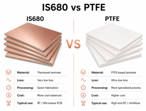
PTFE laminates are often selected for very low-loss RF and microwave circuits. They are widely used in demanding high-frequency designs. However, PTFE materials usually require more specialized processing, which may affect cost, lead time, and manufacturing control.
RO4500 is designed to provide antenna-grade RF performance with easier PCB fabrication. It is often a better fit when the project needs low PIM potential, stable RF behavior, practical manufacturing, and cost-performance balance.
Comparison Item
RO4500 Laminates
PTFE Laminates
Main Advantage
Balanced RF performance and easier fabrication
Very low loss for demanding RF designs
Processing
Similar to standard PCB fabrication
Often requires special processing
PTH Preparation
No special PTFE-style treatment required
More process-sensitive
Cost Control
Good for volume antenna production
Usually higher process cost
Mechanical Handling
More production-friendly
Softer and more sensitive
Typical Use
Antenna PCB, base station antenna, WiMAX
RF, microwave, radar, premium antenna systems
RO4500 is often the better choice when manufacturability, low PIM performance, and production stability matter together. PTFE may be preferred when ultra-low loss is the top design priority.
What Should Be Considered When Designing RO4500 Antenna PCBs?
Designing antenna PCBs with RO4500 requires attention to key details that directly impact RF performance, production repeatability, and long-term reliability. These considerations cover material properties, fabrication processes, and assembly practices, ensuring the final PCB meets design requirements and application needs. Below are the critical points to keep in mind during the design process.
Dk and Design Dk: Process Dk and design Dk are not always the same. Process Dk is mainly used for material control, while design Dk is more useful for circuit simulation. For antenna PCBs, using the correct Dk value helps improve impedance and frequency prediction.
Copper Foil Type: Copper foil affects insertion loss, PIM behavior, and etching quality. Low-profile copper is often preferred in RF applications because smoother copper can help reduce conductor loss.
Impedance Control: Antenna PCB traces must be controlled by line width, dielectric thickness, copper thickness, and layer structure. Even small deviations can affect RF performance, so impedance requirements should be confirmed before fabrication.
Board Thickness and Flatness: Antenna PCBs may have larger board sizes than standard circuit boards. Flatness and dimensional stability should be reviewed carefully, especially for base station antenna boards and large RF panels.
Via and PTH Reliability: RO4500 is easier to process than many PTFE materials, but via quality still matters. Drill quality, hole wall treatment, copper plating, and thermal stress reliability should be controlled during fabrication.
Surface Finish: Surface finish affects solderability, contact reliability, and RF performance. ENIG, immersion silver, OSP, and other finishes may be selected depending on assembly needs and RF contact requirements.
RF Connector Assembly: RF connector layout and soldering quality can affect impedance and PIM performance. Connector footprints, ground via placement, solder joints, and mechanical support should be reviewed before production.
Fabrication Capability: The PCB manufacturer should understand Rogers laminate handling, controlled impedance, RF trace accuracy, low PIM requirements, and inspection control. A proper DFM review before production can help reduce avoidable revisions.
FAQs About RO4500 High-Frequency Laminates
Q1: What is the difference between RO4500 and FR-4 laminates for antenna PCBs?
A1: The core difference lies in RF performance and application scenarios. FR-4 is a standard PCB material with higher dielectric loss (Df) and unstable dielectric constant (Dk) at high frequencies, making it unsuitable for high-frequency antenna designs. RO4500 is a high-frequency laminate specifically engineered for antennas, with controlled Dk (3.3-3.5 ±0.08), low Df (0.0020-0.0037 at 2.5 GHz), and low PIM performance, while also being compatible with conventional FR-4 fabrication processes.
Q2: What is the maximum operating temperature of RO4500 laminates?
A2: RO4500 has a glass transition temperature (Tg) greater than 280°C, which means it can maintain stable mechanical and electrical properties in high-temperature environments. Its maximum continuous operating temperature is typically around 150°C, and it can withstand the high temperatures of lead-free soldering processes (up to 260°C for short durations), making it suitable for harsh industrial and communication infrastructure applications.
Q3: Does RO4500 require special storage conditions?
A3:Yes, RO4500 laminates need proper storage to maintain their performance. They should be stored in a clean, dry environment with relative humidity between 30%-60% and temperature between 15°C-30°C, avoiding direct sunlight, moisture, and chemical contamination. Unopened laminates have a shelf life of 6-12 months; once opened, they should be used within 30 days to prevent moisture absorption affecting dielectric properties.
Q4: Can RO4500 be used for 5G base station antenna PCBs?
A4: Absolutely. RO4500 is widely used in 5G base station antenna PCBs due to its excellent high-frequency performance. Its controlled Dk ensures stable impedance and signal propagation at 5G frequency bands (sub-6GHz and mmWave), low Df reduces signal loss, and low PIM performance (better than -155 dBc) prevents signal interference, which is critical for 5G communication quality.
Q5: What is the moisture absorption rate of RO4500 laminates?
A5: RO4500 has extremely low moisture absorption, typically less than 0.04% (per IPC-TM-650 2.6.2.1 standard). This low moisture absorption ensures that its dielectric properties (Dk and Df) remain stable even in humid environments, avoiding signal degradation and improving the long-term reliability of antenna PCBs.
Q6: Is RO4500 compatible with lead-free soldering processes?
A6: Yes, RO4500 is fully compatible with high-temperature lead-free soldering processes. Unlike traditional PTFE laminates that require special treatment, RO4500 can withstand the 260°C soldering temperature required for lead-free soldering without warping, delamination, or damage to its electrical properties, reducing manufacturing complexity.
Q7: What is the typical cost difference between RO4500 and PTFE laminates?
A7: RO4500 is more cost-effective than PTFE laminates. On average, RO4500 costs 30%-50% less than PTFE laminates for the same thickness and copper weight. This is because RO4500 is compatible with conventional PCB fabrication processes, eliminating the special processing costs required for PTFE, making it more suitable for volume production of antenna PCBs.
Conclusion
In summary, RO4500 stands out as a reliable, cost-effective high-frequency laminate solution for antenna PCB design, balancing excellent RF performance, including stable dielectric properties, low loss, and low PIM with easy manufacturability, making it an ideal choice for wireless infrastructure and various antenna-related applications when paired with thoughtful material selection and design considerations.
Multilayer Ceramic Circuit Board is a circuit structure built with multiple conductive layers inside or on a ceramic substrate. Instead of using glass-reinforced epoxy, like a standard FR4 board, it uses ceramic materials such as alumina, aluminum nitride, silicon nitride, or low-temperature co-fired ceramic materials. These materials give the board strong thermal performance, stable electrical behavior, and excellent mechanical reliability in demanding applications.
A multilayer ceramic substrate is usually designed with several internal layers. These layers may include signal traces, ground planes, power planes, buried vias, thermal vias, and pads for components. The internal structure allows engineers to place more circuits into a smaller area while keeping the board stable and efficient. Compared with a single-layer ceramic board, the multilayer version offers more design freedom and better electrical integration.
The term “multilayer ceramics” can refer to different technologies. Some boards are made by stacking ceramic green sheets and co-firing them with metal paste. Others use post-fired ceramic substrates with plated copper structures. The right technology depends on the required line width, copper thickness, thermal conductivity, operating frequency, and production volume.
How Does a Multilayer Ceramic PCB Work?
Multilayer ceramic PCB works by combining several conductive layers with insulating ceramic layers. Each conductive layer has a specific electrical role. Some layers carry signals, some distribute power, and some act as ground planes.
The ceramic material acts as the dielectric body. It separates the copper, tungsten, molybdenum, silver, or gold conductor layers while providing electrical insulation. At the same time, ceramic conducts heat better than many organic PCB materials. This allows heat generated by power devices, LEDs, resistors, or RF components to move away from hot spots more efficiently.
In high-speed or RF designs, the ceramic substrate also helps keep electrical performance stable. Ceramic materials usually have controlled dielectric properties, low moisture absorption, and good dimensional stability. This helps the board maintain signal quality across temperature changes and long-term use.
A typical multilayer ceramic circuit structure may include:
Signal layers for routing compact circuits and component connections.
Ground layers for shielding, return current control, and noise reduction.
Power layers for stable voltage distribution.
Via structures for vertical interconnection between layers.
Thermal paths for transferring heat from components to the base or housing.
The design principle is simple, but the execution requires precision. The inner layers must align correctly. Via filling must be reliable. The ceramic body must be fired or processed under controlled conditions.
Item
Standard FR4 Multilayer Circuit Board
Multilayer Ceramic Circuit Board
Base Material
Glass fiber and epoxy resin
Alumina, AlN, Si₃N₄, LTCC, or other ceramics
Thermal Conductivity
Moderate
High to very high, depending on ceramic type
Dimensional Stability
Good for common electronics
Excellent under heat and harsh use
Moisture Absorption
Higher than ceramic
Very low
Common Use
Consumer electronics, control boards, general PCB assemblies
Power electronics, RF modules, sensors, medical, automotive, LED, aerospace
Main Advantage
Cost efficiency and broad availability
Heat control, compact structure, high reliability
How Is a Multilayer Ceramic Circuit Board Manufactured?
The manufacturing process depends on the selected ceramic technology. However, the general target is always the same: create a stable ceramic body with precise internal conductive layers and reliable vertical interconnections. For this reason, the process requires strict control of materials, layer registration, firing temperature, conductor shrinkage, and surface finish.
For LTCC and HTCC structures, production often starts with ceramic green tape. This tape is a flexible ceramic sheet before firing. The manufacturer punches or drills via holes, fills them with conductive paste, prints circuit patterns, stacks the layers, laminates them under pressure, and then fires the structure at a controlled temperature. During firing, the ceramic and conductor system become a solid integrated body.
For post-fired ceramic PCB manufacturing, the ceramic substrate may be prepared first, and then copper circuits are built by metallization, plating, etching, or film deposition. This route is often used when higher copper conductivity or thicker copper is needed.
A common multilayer ceramic PCB manufacturing flow may include:
Material selection: Choose alumina, AlN, Si₃N₄, LTCC, or another ceramic based on heat, dielectric, and mechanical needs.
Stack-up design review: Confirm layer count, conductor width, spacing, via size, dielectric thickness, and thermal path.
Via formation: Create vertical holes by punching, laser processing, or drilling, depending on the process.
Via filling and conductor printing: Fill vias and print inner circuit layers using suitable conductive material.
Layer stacking and alignment: Stack all layers with accurate registration to protect electrical continuity.
Lamination or bonding: Press layers together under controlled temperature and pressure.
Firing or metallization: Sinter the ceramic body or build copper after ceramic firing.
Surface finishing: Apply suitable finish for soldering, wire bonding, or component attachment.
Inspection and testing: Use visual inspection, electrical testing, dimensional measurement, and reliability checks.
EBest Circuit (Best Technology) supports ceramic PCB manufacturing with engineering review, material selection, DFM feedback, and production process control. For multilayer ceramic projects, this early review is especially useful because design choices made at the beginning directly affect yield, cost, and long-term product reliability.
What Should Be Considered in Multilayer Circuit Board Design?
Multilayer circuit board design for ceramic substrates requires a slightly different mindset from FR4 design. Engineers should not treat ceramic as just another base material. Ceramic has its own processing rules, strength profile, copper bonding behavior, dielectric behavior, and thermal characteristics.
The first point is material choice. Alumina is widely used because it offers good insulation, stable performance, and attractive cost control. Aluminum nitride is preferred when thermal conductivity is a key requirement. Silicon nitride is useful where mechanical toughness and thermal cycling resistance matter. LTCC materials are often selected for compact RF modules, sensors, and embedded passive designs.
The second point is the layer structure. Engineers should decide which layers will carry signals, which layers will act as ground, and which paths will move heat away from components. In compact power or RF designs, a ground plane is not only an electrical reference. It may also help reduce noise, improve shielding, and stabilize impedance.
Designers also need to consider via diameter, via pitch, conductor thickness, minimum spacing, solder pad size, board thickness, edge clearance, and surface finish. Ceramic is hard and dimensionally stable, which is excellent for many uses.
Here is a practical design comparison:
Design Factor
Why It Matters
Engineering Recommendation
Ceramic Material
Affects heat transfer, dielectric behavior, cost, and strength
Select material according to power, frequency, size, and environment
Layer Count
Controls routing density and board thickness
Use only the required number of layers to balance function and cost
Via Structure
Determines vertical connection and current path
Match via size and filling method with process capability
Ground Plane
Improves signal return path and shielding
Use continuous ground where RF or high-speed signals are present
Thermal Path
Reduces component temperature rise
Place thermal vias or heat-spreading layers close to heat sources
Copper Thickness
Affects current carrying and heat spreading
Choose based on current load and assembly needs
Pad Design
Affects solder quality and component stability
Follow component footprint and ceramic process rules
Surface Finish
Affects solderability and wire bonding
Select ENIG, silver, gold, or other finish based on assembly method
A well-designed multilayer ceramic board is not only smaller. It is also easier to assemble, easier to test, and more reliable in service. Therefore, engineers should involve the manufacturer early, especially when the design includes fine lines, high thermal load, RF routing, or special component packaging.
How Are Inner Layers Connected in a Multilayer Ceramic PCB?
Inner layers in a multilayer ceramic PCB are connected through vias. These vias create vertical electrical paths between different conductive layers. Without vias, each layer would remain isolated, and the board could not function as an integrated multilayer circuit.
The via structure may vary according to the ceramic process. In co-fired ceramic technology, vias are usually formed in the green tape before firing. They are then filled with conductive paste. After stacking and firing, the via becomes part of the ceramic body. In plated ceramic processes, vias may be laser-drilled or mechanically processed, then metallized and plated to form a conductive barrel.
There are several via types that may be used in multilayer ceramic designs:
Via Type
Description
Typical Use
Through Via
Connects from the top layer to the bottom layer
General interconnection and test access
Blind Via
Connects an outer layer to one or more inner layers
Compact routing and HDI-style layouts
Buried Via
Connects only internal layers
Dense routing without occupying outer-layer space
Filled Via
Via hole is filled with conductive or non-conductive material
Heat transfer, current carrying, or flat pad support
Thermal Via
Designed mainly to move heat
Power devices, LEDs, modules, and heat-sensitive circuits
For power electronics, vias must also carry current and heat. A via that only works electrically may not be enough. The designer may need a via array under power components, a copper-filled structure, or direct thermal connection to a metal base or heat sink. In RF circuits, via placement affects grounding and shielding. Poor via distribution can increase parasitic effects, while a carefully designed via fence can improve isolation.
Can Multilayer Ceramic PCBs Support High-Density Circuits?
Yes, multilayer ceramic PCBs can support high-density circuits when the process and design rules are properly matched. Their multilayer structure allows more routing channels within a smaller footprint. This is helpful for compact modules, sensor packages, RF front-end circuits, LED arrays, power control units, and advanced industrial electronics.
High-density design is not only about placing many traces in a small area. It also requires stable insulation, precise via registration, controlled conductor geometry, and reliable assembly pads. Ceramic substrates offer strong dimensional stability, which helps maintain fine features during processing and use.
LTCC is especially useful for compact high-density designs. It can integrate internal conductors, vias, cavities, and sometimes passive structures. This makes it suitable for RF modules, filters, antennas, sensor packages, and compact electronic assemblies.
For dense ceramic circuit boards, engineers should pay attention to:
Routing priority: Place sensitive signals first, then power and support traces.
Ground control: Use ground planes and via stitching to manage return paths.
Thermal mapping: Identify heat sources before finalizing layer placement.
Assembly clearance: Keep enough room for soldering, inspection, and rework evaluation.
Panelization: Consider breakaway design, edge strength, and handling during production.
Testing access: Add test points or inspection features where space allows.
A high-density multilayer ceramic substrate can be powerful when designed with discipline. It can reduce module size while improving heat flow and electrical stability.
What Are the Benefits of Multilayer Ceramic Circuit Boards?
The benefits of multilayer ceramic circuit boards come from the combination of ceramic insulation, dense interconnection, and excellent thermal behavior.
One major benefit is thermal management. Ceramic materials can transfer heat more effectively than many organic PCB materials. Aluminum nitride, in particular, offers high thermal conductivity, making it suitable for power modules, high-brightness LEDs, laser devices, and compact electronics with concentrated heat sources.
Another benefit is electrical stability. Ceramic substrates usually have low moisture absorption and stable dielectric properties. This supports RF performance, high-frequency behavior, and long-term signal integrity. For products working in changing temperatures or demanding environments, that stability is highly valuable.
Mechanical and chemical resistance also matter. Ceramic boards can perform well in high-temperature, high-voltage, or chemically challenging conditions. They keep their shape well and provide a strong platform for precision circuits.
Key benefits include:
Efficient heat dissipation for power components and high-brightness devices.
Compact multilayer routing for smaller electronic modules.
Stable dielectric behavior for RF, sensor, and high-frequency circuits.
Low moisture absorption for dependable operation in harsh environments.
Strong insulation for high-voltage or high-reliability circuits.
Excellent dimensional stability for precise assembly and fine features.
Good long-term reliability for automotive, medical, aerospace, and industrial uses.
Compared with a standard multilayer circuit board, ceramic multilayer technology is not always chosen for basic consumer electronics. Its value becomes clear when the application needs heat control, compact design, stable electrical properties, or rugged operation.
What Are the Common Applications of Multilayer Ceramic PCBs?
Multilayer ceramic PCBs are used in applications where performance, space, and reliability are all important. They are especially valuable when the circuit must handle heat, maintain electrical stability, or operate in demanding conditions..
In power electronics, ceramic boards are used for modules, drivers, converters, inverters, and power control systems. The ceramic body helps move heat away from power semiconductors. This supports better operating temperature control and longer component life.
In RF and microwave devices, ceramic materials provide stable dielectric behavior. This makes them suitable for filters, antennas, amplifiers, radar-related modules, communication systems, and high-frequency sensor packages.
In medical electronics, ceramic boards may be used in sensors, diagnostic modules, imaging equipment, wearable devices, and precision control systems. These products often require stable performance, compact design, and dependable insulation.
In automotive and aerospace electronics, ceramic multilayer boards support harsh-environment applications, including power control, sensor systems, lighting, and communication modules.
Common application areas include:
Power modules and semiconductor packaging.
High-brightness LED and laser systems.
RF and microwave communication modules.
Industrial sensors and control circuits.
Medical diagnostic and monitoring equipment.
Automotive electronics and EV-related power systems.
Aerospace, UAV, and defense-grade electronic modules.
High-temperature electronics and precision instruments.
The application range continues to expand because electronics are becoming smaller, hotter, and more function-rich. A multilayer ceramic circuit structure helps engineers fit more capability into limited space while keeping the product stable and manufacturable.
How Do You Choose a Reliable Multilayer Ceramic PCB Manufacturer?
Choosing the right manufacturer is one of the most important decisions in a multilayer ceramic PCB project. Ceramic multilayer boards require more than basic PCB production ability. The manufacturer should understand ceramic materials, stack-up control, via processing, metallization, firing behavior, surface finish, assembly compatibility, and inspection standards.
A reliable manufacturer should first review the design from an engineering perspective. This includes checking material choice, conductor width, spacing, via size, layer count, thermal path, pad design, and expected assembly method. Good DFM feedback can help engineers improve the design before production begins. This saves time and improves first-pass success.
The manufacturer should also have experience with different ceramic materials. Alumina, aluminum nitride, silicon nitride, LTCC, and other multilayer ceramics do not behave the same way during processing. Each material has its own thermal performance, mechanical strength, dielectric value, and processing window.
Quality control is another key factor. Ceramic boards should be inspected for dimensions, layer alignment, circuit continuity, surface quality, plating quality, solderability, and visual defects. For advanced projects, additional checks such as X-ray inspection, cross-section analysis, thermal testing, and reliability testing may be needed.
When evaluating a manufacturer, engineers can use this checklist:
Evaluation Point
What to Check
Why It Matters
Ceramic Material Capability
Alumina, AlN, Si₃N₄, LTCC, DPC, DBC, or other options
Ensures the right substrate for thermal and electrical needs
Multilayer Process Experience
Layer alignment, via filling, lamination, firing, metallization
Protects inner-layer reliability
DFM Support
Stack-up review, pad review, via review, process advice
Reduces design risk before fabrication
Testing Capability
Electrical test, dimensional inspection, visual inspection, X-ray when needed
Clear feedback, fast response, practical suggestions
Helps projects move faster and with fewer revisions
Traceability
Material batch, process record, inspection data
Supports quality control and regulated applications
EBest Circuit (Best Technology) can support customers from ceramic PCB design review to fabrication and assembly-related engineering discussion. For multilayer ceramic projects, the team can help evaluate material options, stack-up feasibility, via structure, surface finish, thermal path, and manufacturing risk. This is especially helpful for engineers working on power electronics, RF modules, medical devices, industrial control systems, LED products, UAV electronics, and high-reliability applications.
Are you looking for a high-frequency laminate for smaller, more stable, and easier-to-manufacture RF circuit boards?RO4360G2 is a Rogers high-frequency laminate designed for RF applications that need stable dielectric performance, low signal loss, compact circuit size, and reliable PCB fabrication. With its high dielectric constant, low dissipation factor, good thermal behavior, and FR-4-like processing, RO4360G2 is widely used in power amplifiers, small cell transceivers, patch antennas, radar circuits, and other high-frequency boards. This article explains its material properties, datasheet values, applications, design factors, manufacturing process.
What Is RO4360G2?
RO4360G2 is a high-frequency circuit material from Rogers Corporation’s RO4000® laminate family. It is a low-loss, glass-reinforced, hydrocarbon ceramic-filled thermoset laminate designed for RF and microwave circuit applications. Rogers lists the material with a process Dk of 6.15 ± 0.15 and a design Dk of 6.4, which helps reduce circuit dimensions when board size and cost matter.
Unlike many PTFE-based RF materials, RO4360G2 is designed for easier fabrication. Rogers states that it processes similarly to FR-4 and supports automated assembly, while also offering low loss, high thermal conductivity, low Z-axis CTE, and lead-free process compatibility.
In RF circuit board manufacturing, RO4360G2 is commonly selected for:
RF power amplifier boards
Small cell transceiver PCBs
Patch antenna circuits
Ground-based radar boards
Compact RF modules
Communication system boards
Multilayer high-frequency PCB designs
For RF projects, RO4360G2 offers a strong balance between RF performance and manufacturing practicality. It supports compact high-frequency design while keeping fabrication more manageable than many specialty RF substrates.
RO4360G2 High-Frequency Laminates Datasheet
The RO4360G2 high-frequency laminates datasheet provides the main electrical, thermal, mechanical, and processing data needed for RF PCB material selection and fabrication planning. It helps confirm whether the laminate is suitable for the required frequency range, impedance target, board thickness, copper weight, and assembly process. Below is a table and attached PDF file for RO4360G2 for your reference:
Before starting a RO4360G2 circuit board project, the datasheet should be reviewed together with the stackup, impedance requirements, copper thickness, dielectric spacing, surface finish, and assembly conditions. This helps ensure the selected laminate matches both the RF performance target and the fabrication process.
What Are Applications of RO4360G2?
RO4360G2 is used in RF and microwave circuits where compact size, stable electrical behavior, and practical board construction are important. Rogers lists base station power amplifiers, small cell transceivers, patch antennas, ground-based radar, and general RF applications as typical use cases. Here are applications of RO4360G2:
Base Station Power Amplifiers
Small Cell Transceivers
Patch Antennas
Ground-Based Radar
Communication System Boards
Compact RF Modules
How Does RO4360G2 Compare to Other High-Frequency Laminates?
RO4360G2 is often compared with FR-4, PTFE-based laminates, and other Rogers high-frequency materials. The right material depends on frequency, circuit size, insertion loss target, stackup structure, and production cost.
Compared with standard FR-4, RO4360G2 is much better suited for RF applications. FR-4 is widely used for general electronics, industrial control boards, consumer products, and many digital circuits. However, RF designs often need more stable dielectric behavior and lower signal loss. RO4360G2 is designed for high-frequency circuit applications and still processes similarly to FR-4, which gives it a practical manufacturing advantage.
Compared with PTFE-based high-frequency laminates, RO4360G2 offers easier processing. PTFE materials can provide strong RF performance, but they often need more specialized handling during drilling, hole preparation, lamination, and plating. Rogers describes RO4360G2 as a lower total PCB cost solution than competing PTFE products while offering low loss and high thermal conductivity.
Comparison Item
RO4360G2
FR-4
PTFE-Based RF Laminate
RF Suitability
Suitable for many RF and microwave designs
Better for general electronics
Suitable for advanced microwave designs
Dielectric Constant
High Dk, 6.15 process value
Varies and not RF-focused
Depends on material grade
Circuit Size
Supports compact RF structures
Larger RF structures may be required
Depends on Dk
Fabrication
Similar to FR-4
Standard PCB process
Often more process-sensitive
Cost Position
Balanced RF performance and manufacturability
Economical for standard PCBs
Often higher material and process cost
Common Use
RF amplifiers, antennas, radar, small cells
Digital and control circuits
Advanced RF and microwave circuits
The comparison does not mean that one laminate is always better. Each material has a suitable use case. RO4360G2 is a strong material choice when the project needs compact RF geometry, stable high-frequency properties, reliable manufacturing, and reasonable production cost.
Why Use Rogers RO4360G2 for High-Frequency Circuit Boards?
Rogers RO4360G2 is used for high-frequency circuit boards because it brings together high Dk, low loss, good thermal behavior, FR-4-like processing, lead-free compatibility, and multilayer design flexibility.
The high Dk is especially helpful for compact RF layouts. When the dielectric constant is higher, RF traces and resonant structures can often become smaller. This can help reduce board size or leave more space for other components. Rogers notes that RO4360G2, with Dk of 6.15 and design Dk of 6.4, allows circuit dimensions to be reduced where size and cost are critical.
The low dissipation factor helps maintain signal quality. In RF circuit boards, material loss directly affects signal transmission. A lower Df supports better energy transfer across RF traces, matching networks, antennas, and amplifier sections.
Thermal behavior also matters. RO4360G2 has a listed thermal conductivity of 0.75 W/m·K, which supports heat transfer better than many standard PCB materials. For power amplifier boards and dense RF modules, this can help improve thermal performance at the board level.
Another reason to use this material is production efficiency. Since RO4360G2 processes similarly to FR-4, PCB factories with high-frequency material experience can produce it with a more controlled process flow. This can help reduce production complexity compared with some PTFE materials.
RO4360G2 also supports multilayer RF circuit board design. It can be paired with RO4400™ prepreg and lower-Dk RO4000 laminate in multilayer constructions. This gives the stackup more flexibility for RF, power, and control circuits within the same PCB.
What Are the Design Considerations for RO4360G2 RF Circuit Boards?
A RO4360G2 RF circuit board should not be treated like a standard FR-4 board with a different material name. The design should consider RF behavior, material thickness, copper roughness, impedance control, thermal path, via structure, and assembly process from the beginning.
Stackup Planning: The stackup should be confirmed before layout finalization. Dielectric thickness, copper weight, prepreg type, and reference plane distance all affect impedance. For multilayer boards, RO4360G2 may be used on selected RF layers while other compatible materials support power or control sections.
Controlled Impedance: RF trace width depends on Dk, dielectric thickness, copper thickness, solder mask condition, and trace geometry. Microstrip, stripline, and coplanar waveguide structures should be calculated and reviewed before production.
Copper Selection: Copper type and surface roughness can affect insertion loss at high frequency. For RF boards, copper selection should match the frequency range and loss target.
Via Design: Via transitions can introduce discontinuities in RF paths. Ground vias, via fences, back drilling, and controlled via spacing may be required depending on the frequency and layout.
Solder Mask Clearance: Solder mask can change impedance on exposed RF traces. Many RF designs require careful solder mask opening around transmission lines, antennas, and tuning structures.
Thermal Path: Power amplifier and radar circuits may generate concentrated heat. Thermal vias, copper areas, metal backing, and heat-spreading structures should be reviewed early.
Panelization and Routing: RF boards may be sensitive to edge accuracy, board flatness, and dimensional tolerance. Panel design should consider routing, breakaway tabs, fiducials, and inspection requirements.
Surface Finish: ENIG, immersion silver, and other finishes may be selected depending on solderability, RF performance, storage condition, and assembly process. The final choice should match both electrical and manufacturing needs.
How Is RO4360G2 High-Frequency PCB Manufactured?
RO4360G2 high-frequency PCB manufacturing needs careful control of material, stackup, trace accuracy, and impedance. Although this laminate can be processed similarly to FR-4, RF boards still require tighter fabrication control because small changes in dielectric thickness, copper width, or plating can affect signal performance.
1. Material and Stackup Confirmation Before production, the manufacturer should confirm the RO4360G2 laminate grade, dielectric thickness, copper weight, finished board thickness, and layer structure. For multilayer RF PCBs, the stackup must also match the impedance requirement and assembly conditions.
2. CAM and DFM Review The production team reviews Gerber files, drill files, impedance notes, solder mask openings, via structures, and RF trace areas. This step helps find possible manufacturing risks before fabrication starts, such as narrow spacing, unsuitable via design, unclear impedance values, or solder mask issues near RF lines.
3. Imaging and Etching Control RF traces require accurate line width and spacing. During imaging and etching, the factory must control copper compensation, etching speed, and trace tolerance. This is especially important for microstrip, stripline, and coplanar waveguide designs.
4. Lamination for Multilayer Boards For multilayer RO4360G2 PCBs, the laminate, prepreg, copper layers, and inner circuits are bonded under controlled temperature and pressure. Stable lamination helps maintain board flatness, layer alignment, and dielectric consistency.
5. Drilling and Copper Plating Drilling quality affects plated through-hole reliability. The factory should use suitable drilling parameters and then control hole cleaning, copper deposition, and copper plating thickness. Good hole quality helps improve reliability during assembly and long-term use.
6. Solder Mask and Surface Finish Solder mask must follow the RF design requirement. In some RF areas, solder mask clearance is needed to avoid changes in impedance. The surface finish should also match the soldering process, RF performance needs, and storage requirements.
7. Testing and Final Inspection After fabrication, the boards should go through electrical testing, AOI, visual inspection, dimensional inspection, and impedance testing when required. For RF projects, inspection records and impedance reports help confirm that the finished PCB matches the design intent.
In short, RO4360G2 PCB manufacturing is not only about producing the board shape. It is about keeping the material, stackup, trace geometry, hole quality, and impedance under control from the first technical review to final shipment.
Why Choose EBest for Your RO4360G2 Circuit Board Manufacturer?
Choosing EBest for your RO4360G2 circuit board means working with a PCB manufacturer that understands RF material control, impedance accuracy, and high-frequency PCB production. This helps reduce design-to-production risk and makes the manufacturing process more predictable. EBest can support your RO4360G2 project with:
Rogers Material Confirmation: We help confirm laminate grade, dielectric thickness, copper weight, stackup, and surface finish before production. This reduces the risk of material mismatch and specification errors.
RF Stackup and Impedance Review: Our team reviews stackup structure, trace width, dielectric spacing, copper thickness, and impedance notes to help the board meet the intended RF performance.
DFM Review Before Fabrication: We check Gerber files, drill files, solder mask openings, via structures, spacing, and RF trace areas before manufacturing. This helps find potential issues early and avoid costly revisions.
Controlled High-Frequency PCB Manufacturing: EBest controls imaging, etching, lamination, drilling, plating, solder mask, surface finish, and final inspection to support stable RO4360G2 PCB quality.
Prototype and Small-Batch Support: We support 1 piece prototype and small-batch production, helping verify RF performance, assembly fit, and manufacturability before larger production.
PCB Fabrication and PCBA Assembly: EBest can provide bare PCB fabrication, component sourcing, SMT assembly, through-hole assembly, and inspection support when a one-stop solution is needed.
Testing and Quality Records: We can support electrical testing, AOI, visual inspection, dimensional checks, impedance testing, and related quality documentation based on project needs.
If you need RO4360G2 circuit board manufacturing, send your Gerber files, stackup, impedance requirements, BOM, quantity, and delivery target to sales@bestpcbs.com. EBest will review your project and provide practical manufacturing support from PCB fabrication to PCBA assembly.
FAQs About RO4360G2 High-Frequency Laminates
Q1: Which RF products usually benefit from RO4360G2? A1: RO4360G2 is suitable for RF and microwave circuit boards used in base station power amplifiers, small cell transceivers, patch antennas, radar circuits, communication systems, and compact RF modules.
Q2: What dielectric value should be used during circuit planning? A2: Rogers lists RO4360G2 with a process dielectric constant of 6.15 ± 0.15 and a design Dk of 6.4. The design value is commonly used during circuit calculation and simulation.
Q3: Can this laminate work in a hybrid multilayer stackup? A3: Yes. RO4360G2 can be paired with RO4400™ prepreg and lower-Dk RO4000 laminates in multilayer constructions, making it useful for RF, power, and control sections in one PCB.
Q4: Is this material easier to fabricate than PTFE-based RF laminates? A4:In many cases, yes. Rogers describes RO4360G2 as a thermoset laminate that processes similarly to FR-4, while many PTFE-based materials need more specialized handling.
Q5: What files should be prepared before requesting a quotation? A5:It is helpful to prepare Gerber files, drill files, stackup drawings, impedance requirements, material notes, surface finish requirements, BOM if assembly is needed, quantity, and delivery target.
Q6: Which inspections are useful for this type of RF PCB? A6: Common inspection steps include AOI, electrical testing, visual inspection, dimensional checks, and impedance testing when required. For stricter projects, material confirmation and production records may also be useful.
Q7: Can EBest support both bare PCB fabrication and assembly? A7:Yes. EBest can support RO4360G2 bare PCB fabrication, component sourcing, SMT assembly, through-hole assembly, inspection, and related testing support based on the project requirement.
Is RO4835material the right laminate for your next high frequency PCB project? In RF, radar, microwave, antenna, and communication circuits, the PCB substrate has a direct influence on signal loss, impedance stability, phase behavior, and long-term reliability.
Compared with standard FR4, this Rogers laminate offers lower loss, stable dielectric behavior, and improved oxidation resistance. It is also easier to process than many traditional microwave laminates, making it a practical option for projects that need both RF performance and efficient production.
This guide explains its key properties, selection points, manufacturing process, LoPro option, and supplier considerations for high frequency PCB manufacturing.
What Is RO4835 Material?
RO4835 materialis a high frequency circuit laminate from the Rogers RO4000 series. It is designed for RF, microwave, radar, sensor, antenna, and controlled impedance PCB applications where stable electrical performance is required.
Unlike standard FR4, it uses a hydrocarbon ceramic-filled system. This structure gives the laminate a strong balance of low loss, thermal stability, dimensional consistency, and standard PCB process compatibility.
For many high frequency PCB projects, material choice affects:
Impedance control
Insertion loss
Phase stability
Soldering reliability
Long-term service life
In simple terms, this laminate is selected when FR4 cannot provide enough RF consistency, but the product still needs a material that supports efficient PCB manufacturing.
Why Is RO4835 Used in High Frequency PCB Designs?
This laminate is used in high frequency PCB designs because it provides stable dielectric properties, low signal loss, good thermal behavior, and improved oxidation resistance. These features help the board maintain consistent signal performance in RF and microwave circuits.
At lower frequencies, the PCB substrate may not strongly affect the signal. However, as the operating frequency increases, the laminate becomes part of the signal path. The dielectric constant, dissipation factor, copper roughness, trace geometry, and stackup all influence the final result.
Benefits for high frequency PCB designs:
Helps maintain controlled impedance.
Reduces dielectric loss compared with ordinary FR4.
Supports better phase consistency.
Helps antenna and RF circuits stay closer to the target frequency.
Provides better long-term reliability in warmer operating environments.
Works with many standard PCB fabrication methods.
That is why this material is often considered when a project needs stronger RF performance than FR4 while still requiring a practical manufacturing route.
What Is the Dielectric Constant of RO4835?
The dielectric constant of RO4835 is typically 3.48 ± 0.05 at 10 GHz as a process Dk. Its design Dk is commonly listed as 3.66 from 8 GHz to 40 GHz. For 4 mil laminates, the process Dk is usually 3.33 ± 0.05.
Dielectric constant, also called Dk, describes how the PCB laminate stores electrical energy in an electromagnetic field. In high frequency PCB design, this value directly affects signal speed, wavelength, impedance, and resonance behavior.
It is also important to distinguish between process Dk and design Dk. Process Dk is measured under standard test conditions and is often used for material comparison. Design Dk is more useful for circuit modeling because it better reflects practical PCB performance.
For RF, microwave, antenna, and radar circuits, a stable Dk helps the circuit maintain predictable electrical behavior across the target frequency range. This is one of the key reasons RO4835 is selected for high frequency PCB applications.
What Are RO4835 Tan Delta and Loss Performance?
Its typical dissipation factor, also called tan delta or Df, is 0.0037 at 10 GHz. This low-loss characteristic makes the laminate suitable for RF and microwave PCB applications.
Tan delta shows how much signal energy is lost in the dielectric material. A lower value usually means lower dielectric loss, cleaner signal transmission, and better high frequency behavior.
However, total PCB loss does not depend on the laminate alone. It is also affected by copper roughness, trace length, trace width, via transition, surface finish, and final stackup.
Factor
Influence on Performance
Dissipation factor
Affects dielectric loss
Copper roughness
Affects conductor loss
Trace geometry
Influences impedance and insertion loss
Via transition
Impacts return loss and signal continuity
Surface finish
May affect RF loss at higher frequencies
Etching accuracy
Controls final trace width
Stackup consistency
Supports stable signal behavior
For high frequency PCB manufacturing, the material gives a reliable foundation. Still, the final board performance also depends on controlled fabrication, proper stackup design, and accurate process execution.
What Does the RO4835 Datasheet Indicate?
The datasheet shows that this laminate is designed for high frequency circuit applications. It offers low loss, stable dielectric constant, low moisture absorption, good thermal stability, and improved oxidation resistance.
Property
Typical Value
Process Dk
3.48 ± 0.05 at 10 GHz
Design Dk
3.66 from 8–40 GHz
Dissipation factor
0.0037 at 10 GHz
Thermal coefficient of Dk
+50 ppm/°C
Decomposition temperature
390°C
Glass transition temperature
>280°C
Z-axis CTE
31 ppm/°C
Thermal conductivity
0.66 W/m·K
Moisture absorption
0.05%
Flammability
UL 94 V-0
Lead-free process compatibility
Yes
The datasheet helps confirm available laminate thicknesses, copper options, panel sizes, and process compatibility. For RF and microwave PCBs, these details should be checked before layout finalization and production.
RO4835 vs RO4350B: What Is the Difference?
RO4835 and RO4350B are both high frequency laminates from the Rogers RO4000 series. They share similar electrical properties and are widely used for RF, microwave, radar, antenna, and communication circuit boards.
The main difference is that RO4835 offers improved oxidation resistance. This makes it a good option for applications that may experience higher operating temperatures, longer service life, or more demanding environmental conditions.
RO4350B is a mature and common choice for many RF PCB projects. The other option is often selected when the board needs extra long-term thermal stability and improved resistance to oxidation.
Therefore, the choice depends on application conditions. If the PCB will be used in automotive radar, sensor systems, or higher-temperature RF environments, the oxidation-resistant option may offer a stronger reliability margin.
When Should You Choose RO4835 High Frequency PCB?
You should choose this high frequency PCB material when your circuit needs low loss, stable impedance, controlled dielectric behavior, and better reliability than standard FR4 can provide. It is especially suitable for the following PCB projects:
Automotive Radar and Sensor Boards: Radar circuits require stable signal transmission, accurate impedance, and reliable performance over time.
RF Communication Modules: RF modules often need stable transmission lines, matching networks, filters, and antenna feed structures.
Microwave Circuit: At microwave frequencies, material loss and dielectric variation become more critical.
Power Amplifier Boards: Power amplifier circuits need stable electrical performance and good thermal behavior.
Controlled Impedance Multilayer PCBs: The laminate can be used in multilayer and hybrid stackups. However, the stackup must be reviewed carefully to control impedance and lamination quality.
Before choosing this material, it is helpful to check:
Operating frequency
Signal loss requirement
Target impedance
PCB layer count
Copper thickness
Surface finish
Application temperature
Production quantity
Testing requirements
Reliability requirements
It is a good material choice when stable RF performance and long-term reliability are more important than the lowest material cost.
How Is RO4835 High Frequency PCB Manufactured?
High frequency PCB manufacturing requires tighter process control than standard FR4 PCB fabrication. For RF, microwave, radar, and antenna circuits, small changes in line width, dielectric thickness, copper thickness, or plating quality may affect impedance and signal performance. Therefore, each production step should be carefully reviewed and controlled.
1. Material Confirmation
The first step is to confirm the laminate type, material thickness, copper weight, panel size, and batch information. This helps ensure that the selected laminate matches the approved stackup and customer specification. Batch information is also important for production traceability, especially for RF and high-reliability PCB projects.
2. Stackup Review
Before production starts, the stackup should be reviewed according to impedance requirements, dielectric thickness, copper thickness, layer count, and reference layer structure. This step helps confirm whether the trace width and spacing can meet the target impedance. A clear stackup review can also reduce production risk before fabrication begins.
3. Inner Layer Imaging and Etching
During inner layer imaging, the circuit pattern is transferred onto the copper surface. After that, the unwanted copper is removed through etching. For high frequency circuits, line width control is especially important because even a small deviation may affect impedance, insertion loss, and signal consistency. Clean imaging and stable etching help maintain accurate RF trace geometry.
4. Lamination
In multilayer PCB production, the inner layers are bonded together through lamination. Pressure, temperature, bonding material, heating rate, and cooling rate should be properly controlled. Good lamination helps maintain board flatness, dielectric consistency, and layer-to-layer alignment. For hybrid stackups, material compatibility should also be reviewed before production.
5. Drilling
Drilling creates through holes, vias, and mounting holes according to the design files. Suitable drill tools, spindle speed, feed rate, and backup materials should be selected to achieve clean hole walls. Good drilling quality supports reliable plating and helps reduce defects such as rough hole walls, smear, burrs, and hole position deviation.
6. Hole Treatment and Metallization
After drilling, the hole walls need to be cleaned and prepared for copper deposition. This process helps remove drilling residue and improves copper adhesion inside the holes. Stable hole treatment is important for plated through-hole reliability, especially in multilayer boards where electrical connection between layers must remain consistent.
7. Copper Plating
Copper plating builds the required copper thickness on the hole walls and board surface. Uniform plating helps improve conductivity, mechanical strength, and long-term reliability. For high frequency boards, plating control should be stable because excessive or uneven copper may influence final trace dimensions and impedance performance.
8. Outer Layer Imaging and Etching
The outer layer circuit pattern is then formed through imaging and etching. Accurate RF trace width, smooth copper edges, and controlled spacing are important at this stage. Since high frequency signals are sensitive to conductor geometry, outer layer etching should be carefully controlled to keep the final circuit close to the designed values.
9. Surface Finish
Surface finish protects exposed copper and improves solderability during assembly. Common options include ENIG, OSP, HASL, and other finishes depending on project requirements. For RF applications, the surface finish should be selected based on solderability, shelf life, assembly process, frequency range, and possible influence on signal loss.
10. Inspection and Testing
Final inspection confirms whether the PCB meets drawing, electrical, and quality requirements. Common checks include AOI, electrical testing, impedance testing, dimensional inspection, visual inspection, and hole quality inspection. For critical RF boards, test coupons may also be used to verify impedance performance before shipment.
This Rogers laminate is easier to process than many PTFE-based microwave materials, but high frequency PCB production still requires careful process control. The final result depends on both material quality and manufacturing accuracy.
Why Choose EBest for RO4835 PCB Manufacturing?
EBest supports high frequency PCB manufacturing with practical production experience and one-stop service from PCB fabrication to PCBA assembly. Here are reasons why choose EBest for RO4835 PCB manufacturing:
Laminate selection support: We help customers review laminate thickness, copper weight, stackup structure, and application requirements before production.
High frequency PCB manufacturing capability: We support RF, microwave, radar, sensor, antenna, communication, and controlled impedance PCB projects.
Controlled impedance PCB support: We can assist with impedance stackup review, trace width control, impedance coupon planning, and production testing.
FreeDFM review before production: We check manufacturability details such as trace width, spacing, via structure, copper balance, drilling, surface finish, and panel design.
Multilayer and hybrid stackup production: We support multilayer PCB and hybrid PCB structures based on project requirements.
Prototype and small-batch manufacturing: We help customers move from sample verification to stable production with flexible order support.
Turnkey PCBA assembly service: In addition to PCB fabrication, we can provide component sourcing, SMT assembly, DIP assembly, testing, and final inspection.
Reliable component sourcing: We help customers source suitable components for RF, communication, industrial, automotive, medical, and control applications.
Quality inspection and testing: Our quality process can include AOI, X-ray inspection, electrical testing, impedance testing, functional testing, and final quality checks.
Traceability support: We provide production traceability for material, process, inspection, and shipment records.
Support for demanding industries: EBest serves customers in communication, industrial control, automotive electronics, medical devices, aerospace/UAV, RF modules, and high-performance electronics.
For high frequency PCB projects using Rogers materials, EBest can help customers reduce design-to-production risk, improve production consistency, and build reliable RF circuit boards from prototype to volume production.
FAQs About RO4835 Material
Q1: What does RO4835 LoPro mean? A1:RO4835 LoPro refers to a laminate option using low-profile copper. Low-profile copper can help reduce conductor loss at higher frequencies, especially when the circuit has long RF traces, tight insertion loss targets, or sensitive phase requirements.
Q2: When should I choose RO4835 LoPro instead of standard copper? A2:Choose the LoPro option when conductor loss is a major concern. It is especially useful for microwave circuits, radar boards, antenna feed lines, and high-speed RF transmission paths where copper surface roughness may affect signal quality.
Q3: Can this laminate replace FR4 in every high frequency PCB? A3:Not always. It is a better fit when the circuit needs low loss, stable impedance, and reliable RF behavior. For simple low-frequency boards, FR4 may still be more economical.
Q4: Is this material suitable for lead-free assembly? A4: Yes. Its high thermal stability helps the board withstand common lead-free reflow and soldering processes.
Q5: Can it be combined with FR4 in one multilayer PCB? A5:Yes. It can be used in hybrid multilayer PCB structures. However, the stackup, bonding material, lamination cycle, and thermal expansion behavior should be checked before production.
Q6: What files are needed for a quotation? A6: A complete quotation usually requires Gerber files, drill files, stackup information, copper thickness, surface finish, board thickness, impedance requirements, quantity, and assembly details if PCBA service is needed.
Q7: How can EBest help with this type of PCB project? A7:EBest can support material review, DFM checking, controlled impedance production, PCB fabrication, component sourcing, PCBA assembly, inspection, testing, and production traceability.
Contact Us for Custom High Frequency PCB Quotation
Looking for a reliable manufacturing partner for your high-frequency PCBs? EBest helps you reduce production risk with material selection support, controlled impedance review, DFM feedback, precise fabrication, and one-stop PCBA assembly.
Whether your project involves RF modules, radar boards, microwave circuits, antenna PCBs, or communication equipment, our team can help you move from prototype to production with better consistency and fewer delays.
Send your Gerber files, stackup requirements, quantity, and technical notes to sales@bestpcbs.com today. We will review your project and provide a fast, practical quotation for your high-frequency PCB needs.
Acrylic conformal coating is a thin, transparent protective film applied over a printed circuit board to shield sensitive circuits from moisture, dust, light chemical exposure, salt mist, mild corrosion, and general environmental stress. In PCB assembly, it is often used when the electronics must remain reliable after leaving a clean factory environment and entering real operating conditions, such as industrial cabinets, medical devices, outdoor controls, automotive modules, LED systems, consumer electronics, and communication equipment.
The coating is called “conformal” because it follows the shape of the PCB surface. It covers solder joints, component leads, copper traces, exposed pads, and surface-mounted devices with a uniform protective layer. Unlike potting compound, which fully encapsulates the circuit, acrylic coating remains relatively thin and lightweight. This makes it suitable for assemblies where space, weight, inspection, and repairability still matter.
The main resin system in this type of coating is acrylic. Once applied and dried, it forms a hard but flexible protective film. Most acrylic coatings are clear, which allows engineers and quality teams to inspect markings, solder joints, component orientation, and general workmanship after coating. This is one reason conformal coating acrylic materials are popular in PCBA production. They offer a clean visual finish while improving board-level protection.
In practical electronics manufacturing, acrylic coating is valued because it is easy to apply, dries quickly, and is easier to remove than many other coating families. This makes it attractive for prototypes, medium-volume production, and products that may need future rework. For example, when a component must be replaced, acrylic conformal coating removal is usually more straightforward than removing urethane or silicone coating. Technicians can often use compatible solvents, localized abrasion, or controlled repair methods depending on the coating chemistry and board design.
For PCB manufacturers and assembly partners such as EBest Circuit (Best Technology), acrylic coating can be part of a wider reliability strategy. A coating does not replace proper PCB design, soldering control, cleanliness, material selection, or testing. Instead, it works together with these process controls. When applied correctly, it helps create a more dependable assembly for customers who need stable performance in humid, dusty, or mildly corrosive environments.
Acrylic coating is commonly available in liquid form for brushing, dipping, and spraying. It can also be formulated as an acrylic conformal coating spray for convenient manual application or repair. Some advanced production lines use selective coating machines to apply the film only to defined areas while keeping connectors, test points, switches, sensors, heat sinks, and other keep-out zones free of coating.
In short, this coating is a practical, clear, and efficient PCB protection method. It is widely used because it balances protection, process speed, appearance, and reworkability. For many electronic products, that balance is more valuable than choosing the thickest or most chemically resistant material.
How to spray acrylic conformal coating?
Spraying is one of the most common application methods for acrylic coating, especially when the production team wants a smooth, even, and visually clean finish. It can be done with aerosol cans, handheld spray guns, automated spray systems, or selective coating equipment. The right method depends on volume, board complexity, coating thickness requirement, masking needs, and quality expectations.
Before spraying, the PCB assembly must be clean and dry. This step is more important than many people realize. Flux residue, fingerprints, dust, moisture, ionic contamination, and handling marks can reduce coating adhesion and create cosmetic or electrical issues. A conformal coating layer is not a magic cover for poor cleaning. It performs best when the board surface is already controlled through a disciplined PCBA process.
A typical spray process starts with inspection and masking. Areas that should not be coated must be protected. These may include connectors, sockets, switches, programming ports, LEDs, display windows, RF shielding contact points, test pads, and mechanical grounding areas. Masking can be done with tapes, boots, caps, liquid mask, or custom fixtures. For higher-volume production, dedicated masking fixtures save time and improve repeatability.
After masking, the operator or machine applies the coating in thin, controlled passes. It is usually better to apply multiple light passes than one heavy wet layer. A heavy layer can trap solvent, cause bubbles, create edge buildup, or produce uneven coverage around tall components. A controlled spray angle also matters. Tall capacitors, transformers, relays, connectors, and shield cans can create shadowed areas. Operators often adjust spray direction to improve coverage around component bodies and solder joints.
A practical spray workflow may look like this:
Clean and dry the assembled PCB before coating.
Mask connectors, test points, switches, sensors, and other keep-out areas.
Mix or prepare the coating according to the supplier’s technical data sheet.
Spray thin, even passes across the board surface.
Allow proper flash-off time between coats if multiple coats are needed.
Inspect the coating under normal light and, if applicable, UV inspection light.
Cure or dry the board under the recommended temperature and time conditions.
Remove masking and complete final quality checks.
Acrylic conformal coating spray is convenient for engineering samples, repair work, and low-volume builds. It allows quick application without complex equipment. However, aerosol spraying requires good operator control. Distance, angle, speed, and overlap can all affect the final coating thickness. For production builds, spray guns or automated systems usually deliver better consistency.
In professional PCB assembly, coating thickness is often checked using wet film gauges, dry film measurement, witness coupons, or other approved methods. The target thickness depends on the coating material, design standard, operating environment, and customer requirement. A thicker coating is not always better. Excessive thickness may create stress, slow drying, affect component cooling, or interfere with connectors and moving parts. The objective is controlled coverage, not simply more material.
Ventilation and safety control are also part of the process. Many solvent-based acrylic coatings release vapors during spraying and drying. Operators should use proper extraction, personal protective equipment, and approved handling practices. The coating material’s safety data sheet should always guide storage, use, and disposal.
At EBest Circuit (Best Technology), coating process planning normally starts with the product application and assembly design. A board used in a medical monitoring device may require different masking, documentation, and inspection control than a lighting module or industrial sensor. Spray application can be highly effective, but it should be supported by clear drawings, coating keep-out definitions, and acceptance standards.
Why choose acrylic coating over other conformal coatings?
Acrylic coating is often selected because it offers a highly practical balance between protection, processing speed, cost control, visual clarity, and repairability. In many PCB projects, the best coating is not the most aggressive material. The better choice is the one that matches the actual operating environment, production process, inspection needs, and lifecycle expectations.
Conformal coating families commonly include acrylic, silicone, urethane, epoxy, parylene, and UV-curable materials. Each has its own strengths. Acrylic is popular because it is easier to apply and remove than many alternatives. It dries relatively fast, offers good moisture and dielectric protection, and creates a clear finish that supports inspection. For many indoor industrial, commercial, medical, control, and electronic assembly applications, this makes acrylic a smart and efficient option.
When people compare acrylic vs silicone conformal coating, the real question is usually about flexibility and temperature. Silicone coatings are often better for very high-temperature environments or assemblies exposed to strong thermal cycling. They remain soft and elastic. Acrylic coatings are harder, cleaner-looking, and easier to handle in many production environments. Acrylic is also generally easier to rework, which is valuable when the product may need component replacement or field repair.
When comparing acrylic vs urethane conformal coating, the discussion often centers on chemical resistance and removal. Urethane coatings are usually chosen for harsher chemical exposure and stronger abrasion resistance. Acrylic coatings are often preferred where fast drying, clean appearance, lower process complexity, and easier rework are more important. Urethane can be more difficult to remove, which may increase repair time.
Here is a clear comparison:
Coating Type
Practical Strengths
Typical Considerations
Best-Fit Applications
Acrylic
Fast drying, clear finish, good moisture protection, easy inspection, easier removal
Moderate chemical resistance compared with urethane; may not be ideal for very high heat
General PCB protection, industrial controls, medical electronics, consumer devices, LED products
Silicone
Excellent flexibility, good high-temperature performance, strong thermal cycling tolerance
Softer surface, may attract dust, repair can be more process-sensitive
For many engineers, acrylic coating becomes the preferred choice because it supports real production needs. It can be sprayed, dipped, brushed, or selectively applied. It dries quickly enough for efficient workflow. It keeps the board readable. It also allows rework when needed, which helps reduce service complexity.
This is especially useful in prototype-to-production projects. A team may still be optimizing BOM choices, connector positions, test methods, or enclosure design. Choosing a highly permanent coating too early can make debugging and changes more difficult. Acrylic gives engineers a useful middle ground. It offers dependable protection while keeping the product more serviceable.
EBest Circuit (Best Technology) often helps customers evaluate coating choices from a manufacturing viewpoint. The decision should consider operating temperature, humidity, chemicals, vibration, cleaning agents, expected service life, inspection requirements, and repair strategy. A material that looks strong on paper may create unnecessary complexity if it does not match the product’s real conditions.
What are the benefits of acrylic conformal coating for PCBs?
The benefits of acrylic coating for PCBs are strongest when the assembly needs clear, lightweight, and cost-conscious protection without making rework overly complicated. For many electronic products, this coating helps improve operational stability while keeping the manufacturing process efficient.
The first major benefit is moisture protection. PCBs may encounter humidity during shipping, storage, installation, or daily operation. Moisture can reduce insulation resistance, encourage corrosion, and create leakage paths between conductive features. A properly applied acrylic film helps reduce direct contact between the board surface and the surrounding environment.
The second benefit is corrosion resistance. Copper, solder joints, component leads, and exposed metal surfaces can be affected by moisture, salt, sulfur compounds, and airborne contaminants. Acrylic coating helps isolate these areas. This is useful for electronics used near coastal areas, factory floors, transportation systems, and equipment rooms where the environment is less controlled than a laboratory.
Another important benefit is dielectric protection. A conformal coating layer helps improve surface insulation between conductive points. This is useful on boards with fine-pitch components, high impedance circuits, compact layouts, and areas where condensation may be present. Good coating coverage helps the circuit maintain more stable electrical behavior over time.
Acrylic coatings also provide a clean visual finish. Since the film is usually transparent, board markings remain visible. This supports inspection, traceability, serial number reading, repair, and quality review. For customers who value tidy workmanship, the final coated board can look refined and professional.
Common advantages include:
Clear appearance for easy inspection and product traceability.
Fast drying compared with many traditional coating systems.
Good protection against humidity, dust, and mild corrosion.
Practical reworkability for component replacement or repair.
Compatible with spray, brush, dip, and selective coating methods.
Suitable for many commercial, industrial, medical, and control electronics.
Lightweight protection without bulky encapsulation.
Balanced cost and process efficiency for production builds.
Acrylic coating also supports manufacturability. It does not usually require the same process complexity as some highly specialized coatings. For many PCBA factories, this means faster line setup, more flexible application methods, and easier operator training. When production volume increases, the process can be upgraded from manual spray to selective coating equipment.
In terms of product design, acrylic coating can help extend the usable life of assemblies operating in humid or dusty conditions. It is especially useful for boards installed inside enclosures that offer some physical protection but are not fully sealed. Examples include control boards, sensor modules, power control boards, LED drivers, instrumentation boards, and medical monitoring electronics.
However, the real benefit depends on application quality. A thin, uniform, well-cured coating performs far better than a thick but poorly controlled layer. Masking, cleanliness, viscosity, spray pattern, curing time, and inspection all influence the result. This is why coating should be treated as an engineered process, not a simple finishing step.
At EBest Circuit (Best Technology), coating can be considered alongside PCB fabrication, component sourcing, assembly, testing, and reliability planning. This integrated view helps customers avoid late-stage surprises. For example, connector keep-out areas, test pad access, conformal coating inspection, and rework strategy can be discussed before mass production begins.
Is UV curable acrylic coating better for mass production?
UV curable acrylic coating can be an excellent choice for mass production when speed, controlled curing, and production throughput are top priorities. Traditional solvent-based acrylic coatings dry as solvents evaporate. UV curable systems cure rapidly when exposed to ultraviolet light. This can reduce waiting time, improve handling speed, and make production flow more predictable.
In high-volume PCBA manufacturing, curing time matters. A coating that takes a long time to dry may require more floor space, more racks, longer work-in-process time, and additional handling control. UV curing can help reduce these pressures. Once the coated board passes through a proper UV curing system, the film can become tack-free and ready for the next process much faster than many conventional materials.
That said, “better” depends on the product. UV curable acrylic coating is powerful when the board geometry allows sufficient UV exposure. Areas under tall components, inside shadowed regions, or beneath certain connectors may not receive enough UV light. Some UV systems use secondary moisture or thermal cure mechanisms to complete curing in shadowed zones. The coating supplier’s technical data must be reviewed carefully.
For mass production, UV systems can offer strong advantages in consistency. Automated dispensing or selective coating equipment can apply the material to defined areas, while UV curing equipment provides controlled energy exposure. This combination supports repeatability, which is valuable for customers with strict quality requirements.
Here is a practical comparison:
Factor
Standard Acrylic Coating
UV Curable Acrylic Coating
Drying/Curing Method
Solvent evaporation or air drying, sometimes with heat assistance
UV exposure, sometimes with secondary cure for shadowed areas
Production Speed
Good for prototypes, low-volume, and medium-volume work
Very strong for high-volume production
Equipment Requirement
Lower; can use spray, brush, dip, or selective systems
Higher; needs UV curing equipment and process control
Shadowed Areas
Less affected by UV access, but still needs drying time
Requires attention to component shadows and coverage
Reworkability
Usually good
Depends on formulation; often still manageable
Process Control
Moderate to high, depending on application method
High when paired with automated coating and curing
UV curable acrylic coating is especially attractive for products where production lines need fast movement from coating to inspection, packaging, or further assembly. It may also reduce solvent-related handling concerns in some formulations. For customers scaling from engineering samples to larger builds, UV technology can improve throughput when the coating design is properly validated.
However, a mass production decision should include testing. Engineers should confirm adhesion, thickness, coverage, curing completeness, environmental resistance, masking quality, and long-term reliability. It is also wise to run sample boards through the intended process before committing to full production. Coating materials can behave differently depending on board layout, component height, solder mask surface, cleaning chemistry, and curing equipment.
EBest Circuit (Best Technology) can support this type of evaluation by reviewing the assembly structure and coating objectives. For some products, standard acrylic spray may be the right answer. For others, UV curable acrylic may provide faster, cleaner, and more scalable production. The best selection is based on evidence from the product, not only on the coating category.
How fast does acrylic conformal coating dry and cure?
Acrylic coating is known for relatively fast drying, which is one reason it is widely used in PCB assembly. The exact drying and curing time depends on the coating formulation, solvent system, applied thickness, airflow, humidity, temperature, board geometry, and whether heat or UV curing is used.
For many solvent-based acrylic materials, the surface can become tack-free within minutes to less than an hour under suitable conditions. Full cure may take longer, often several hours or more depending on the product data sheet. Some coatings reach handling strength quickly but continue to build final film properties over time. This is why production teams should not rely only on touch. A coating may feel dry before it has achieved its final protective performance.
In practical terms, drying has two stages. The first stage is flash-off, where solvents begin to evaporate from the wet film. The second stage is curing or final film formation, where the coating reaches its intended mechanical and protective properties. If the coating is applied too thickly, the top surface can dry while solvent remains trapped underneath. This may lead to bubbles, cloudy appearance, weak adhesion, or longer cure times.
Temperature can speed up drying, but it must be controlled. Excessive heat may affect components, labels, plastics, batteries, displays, or other sensitive parts. Airflow also helps solvent evaporation, but strong uncontrolled airflow can carry dust or create uneven drying. In a professional coating process, drying conditions should be defined and repeatable.
Aerosol acrylic conformal coating spray may become touch-dry fairly quickly, which makes it convenient for repair and prototype work. However, final assembly, testing, packaging, or shipment should follow the recommended cure schedule. For products used in medical, industrial, or transportation environments, proper curing is part of reliability control.
UV curable acrylic systems are much faster when exposed to the correct UV intensity and wavelength. Some can cure within seconds in exposed areas. This makes them attractive for automated production. Still, shadowed areas require attention. If the coating supplier specifies secondary cure requirements, the production process must include them.
A simple way to think about drying speed is this: acrylic coating is usually fast enough for efficient production, but it still requires disciplined process control. The board should not be rushed into packaging or environmental testing before the film has reached the required condition. Handling too early may leave marks, trap solvent, or affect coating uniformity.
Quality teams often verify coating cure through visual inspection, tack testing, thickness measurement, adhesion checks, or process validation records. For more demanding projects, environmental tests may also be used. These can include humidity exposure, thermal cycling, salt mist testing, insulation resistance testing, or customer-defined qualification plans.
EBest Circuit (Best Technology) can help customers define realistic process windows during PCBA production. This is especially important when coating is used on boards with dense components, connectors, transformers, large capacitors, heat sinks, or mixed material surfaces. A good cure schedule protects both product quality and delivery efficiency.
Can acrylic coating protect PCBs from moisture and corrosion?
Yes, acrylic coating can protect PCBs from moisture and corrosion when it is properly selected, applied, cured, and inspected. It creates a protective barrier between the circuit surface and the external environment. This barrier helps reduce moisture contact, surface contamination, oxidation, and corrosion risk on metal features.
Moisture is one of the most common challenges for electronic assemblies. Even when a product is not directly exposed to rain or water, humidity can still enter enclosures. Temperature changes can cause condensation. Dust can absorb moisture. Ionic residues on the PCB surface can become conductive when damp. These conditions may lead to leakage current, corrosion, dendritic growth, unstable signals, or intermittent failures.
Acrylic coating helps by covering vulnerable areas with a continuous film. It protects solder joints, component terminations, copper features, and exposed conductive surfaces. It also helps maintain insulation resistance across the board surface. This is valuable for assemblies used in humid warehouses, industrial facilities, medical environments, HVAC systems, lighting equipment, transportation electronics, and outdoor-adjacent installations.
Corrosion protection is another reason engineers choose this coating. In real operating environments, PCBs may be exposed to airborne salts, cleaning chemicals, sulfur compounds, flux residue, skin oils, or industrial contaminants. A well-applied coating helps reduce direct contact between those contaminants and the board. This supports longer, more stable operation.
However, coating performance depends heavily on cleanliness. If ionic residue or moisture is trapped under the coating, the film may seal in a problem rather than solve it. That is why board cleaning, drying, and inspection must happen before coating. For no-clean flux processes, engineers should still verify compatibility between the flux residue and the coating material. Not every no-clean residue is automatically safe under every coating.
Coverage is also important. Moisture can enter through pinholes, thin edges, uncoated shadow areas, or poorly masked transitions. Sharp component leads, tall solder joints, and board edges may need special attention. Selective coating programs should include coverage checks around dense or high-risk areas.
For products with severe exposure to chemicals, fuel, oils, or continuous outdoor condensation, acrylic may not always be the strongest choice. In such conditions, silicone, urethane, parylene, or special hybrid coatings may be reviewed. Still, for a large range of commercial and industrial PCBs, acrylic coating provides dependable moisture and corrosion protection with a process-friendly profile.
In practical design reviews, it is useful to ask:
Will the board be used indoors, outdoors, or inside a semi-sealed enclosure?
Will it face condensation, salt air, cleaning fluids, or industrial fumes?
Are there high-impedance circuits or fine-pitch components?
Are connectors, switches, sensors, or test pads sensitive to coating contamination?
Will the assembly need future rework or repair?
What inspection and qualification tests are required?
These questions help define whether acrylic coating is the right fit. They also guide masking, thickness, cleaning, and testing requirements. EBest Circuit (Best Technology) can review these details during the early manufacturing stage, helping customers build a coating process that aligns with product use and reliability expectations.
Is acrylic conformal coating suitable for medical devices?
Acrylic coating can be suitable for medical device PCBs when the material, process, documentation, and quality controls match the device’s risk level and operating environment. It is commonly considered for medical monitoring equipment, diagnostic electronics, wearable health devices, control modules, sensor boards, power management boards, and user-interface assemblies.
Medical electronics require stable performance, clean workmanship, traceability, and disciplined process control. The coating material should not be chosen only because it is easy to apply. It should be reviewed in the context of the whole device. This includes enclosure design, sterilization method if applicable, operating temperature, humidity exposure, cleaning agents, electrical requirements, service strategy, and regulatory documentation needs.
For many non-implantable medical electronic assemblies, acrylic coating offers several practical benefits. It provides clear protection against humidity and contamination while allowing visual inspection of component markings and solder quality. It supports rework when properly managed. It also fits well with production processes where traceability and repeatability matter.
In medical PCB assembly, acrylic coating may be used to protect boards inside patient monitoring devices, portable diagnostic tools, test instruments, home healthcare electronics, control panels, and certain wearable devices. These products often operate in environments where cleaning, humidity, and repeated handling are expected. A protective coating can help improve reliability over time.
The suitability also depends on biocompatibility and exposure conditions. If the coating will have direct or indirect patient contact, the material requirements become more specific. If the board is fully enclosed and does not contact the patient, the focus may be more on electrical reliability, process cleanliness, and long-term performance. Engineering and regulatory teams should confirm the required standards for the exact device category.
Process documentation is especially important in medical electronics. A controlled coating process should define the material, batch traceability, application method, coating thickness, masking areas, inspection method, curing parameters, acceptance criteria, and rework procedure. This helps support consistent production and customer audits.
EBest Circuit (Best Technology) has experience supporting PCB and PCBA projects where reliability, documentation, and traceability are important. For medical device PCB assembly, coating should be part of a structured manufacturing plan. The goal is not only to apply a protective film. The goal is to deliver a repeatable, inspectable, and documented assembly that fits the customer’s device requirements.
Acrylic coating is especially useful when medical devices need clear PCB protection without sacrificing repairability. For example, if an engineering team expects future design revisions or component replacement during validation, acrylic is often easier to manage than a more permanent material. It allows teams to protect the board while keeping development practical.
Still, every medical product should be reviewed individually. A board used in a portable monitor may have different requirements from a board used in sterilization equipment or fluid-handling instruments. The right coating choice should come from the application environment, not from a generic material preference.
What industries commonly use acrylic conformal coatings?
Acrylic coatings are used across many industries because they provide clean, efficient, and serviceable PCB protection. They are especially popular in products that need improved resistance to humidity, dust, and mild corrosion while keeping manufacturing flexible.
In industrial electronics, acrylic coatings are often used on control boards, sensor modules, automation equipment, motor control boards, power supplies, and monitoring systems. These products may operate near machinery, dust, oils, vibration, and changing temperatures. A clear protective coating helps maintain circuit stability and supports easier inspection during maintenance.
Medical electronics also use acrylic coatings where the application conditions are appropriate. Patient monitoring devices, diagnostic tools, portable health devices, and laboratory equipment may benefit from moisture and contamination protection. The clear film allows markings and inspection points to remain visible, which is helpful for traceability and quality review.
Automotive electronics may use acrylic coatings in interior modules, control electronics, lighting boards, battery management support boards, and sensor-related assemblies. For under-hood or high-temperature areas, silicone or other materials may sometimes be reviewed, but acrylic remains useful in many protected automotive locations.
Consumer electronics can benefit from acrylic coating when products face humidity, handling, sweat, or environmental dust. Examples include smart home devices, control panels, wearable accessories, audio equipment, handheld electronics, and appliance control boards. The coating improves durability without adding large weight or volume.
LED and lighting products are another common area. LED drivers, lighting control boards, signage modules, and outdoor-adjacent lighting electronics may need protection from moisture and condensation. Acrylic coating helps protect solder joints and circuits while keeping the board visually clean.
Aerospace and transportation applications may also use coating, although the material choice is usually based on strict qualification needs. Acrylic may be suitable for certain protected electronics, while other coating materials may be chosen for more demanding conditions. In these industries, documentation and process validation are extremely important.
Telecommunications and communication equipment often use coatings on control boards, signal boards, power modules, and outdoor cabinet electronics. Humidity and airborne contamination can affect long-term reliability, especially in remote installations or semi-protected environments.
Common industries include:
Industrial control and automation.
Medical electronics and diagnostic devices.
Automotive interior and protected electronic modules.
LED lighting and signage systems.
Consumer and smart home electronics.
Communication and telecom equipment.
Instrumentation and measurement devices.
Power electronics and control systems.
Security electronics and access control devices.
Transportation and equipment monitoring systems.
For each industry, the coating specification should be matched to the actual operating environment. A factory control board, wearable medical device, and LED streetlight driver may all use acrylic coating, but their process requirements may differ. Masking, thickness, cure schedule, cleanliness level, inspection method, and testing plan should be defined separately.
EBest Circuit (Best Technology) supports customers across multiple electronic manufacturing sectors, from PCB fabrication to PCBA assembly and engineering review. For customers using acrylic coatings, early communication is helpful. Coating drawings, keep-out zones, and environmental requirements should be shared before production. This allows the manufacturing team to prepare the correct process route and reduce avoidable delays.
How to apply acrylic conformal coating (spray/dip/brush)?
Acrylic coating can be applied by spray, dip, brush, or selective coating. Each method has its own role in PCB assembly. The best choice depends on production volume, board size, component layout, masking complexity, coating thickness control, cosmetic requirements, and budget.
Spray application is widely used because it produces a smooth and uniform finish. It is suitable for prototypes, batch production, and automated coating lines. Manual spray is flexible, while automated selective spray provides stronger repeatability. Spray is often chosen when the assembly has many components and needs an even coating without immersing the whole board.
Dip coating is efficient for boards that can be fully coated, especially when high throughput is needed and masking is manageable. The board is dipped into a coating tank and withdrawn at a controlled speed. This method can provide complete coverage, including edges and lower surfaces. However, it requires careful masking of connectors and other no-coat areas. It also needs good viscosity control and tank management.
Brush application is simple and useful for repair, prototypes, small areas, or localized touch-up. It does not require expensive equipment. However, brush marks and uneven thickness can occur if the operator is not careful. Brush coating is usually less suitable for high cosmetic requirements or large-volume production, but it remains valuable for engineering work and rework.
Selective coating is the preferred method for many professional production lines. A programmed machine applies coating only to specified areas. This reduces masking labor, improves consistency, and supports repeatable quality. Selective coating is especially useful for boards with many connectors, test points, switches, and coating keep-out zones.
Here is a practical comparison:
Application Method
Main Advantage
Best Use Case
Process Notes
Spray
Smooth finish and flexible coverage
Prototypes, batch builds, automated production
Requires good control of spray distance, angle, and thickness
Dip
Efficient full-board coverage
Simple board designs and larger batches
Requires careful masking and viscosity control
Brush
Low-cost and convenient
Repair, touch-up, small prototypes
Operator skill strongly affects appearance and thickness
Selective Coating
High repeatability and reduced masking
Medium to high-volume PCBA production
Requires programming, fixtures, and process validation
The application process should begin with design review. Engineers should identify where coating is required and where it must be avoided. Connectors, card edges, mechanical contacts, switches, heat dissipation surfaces, microphones, pressure sensors, optical sensors, and test points often need keep-out protection. Clear coating drawings reduce misunderstanding between the customer and manufacturer.
After design review, the board should be cleaned and dried if the process requires it. Cleaning compatibility should be confirmed with the flux system, components, labels, and coating material. Sensitive components should be reviewed before exposure to solvents or heat.
Masking comes next. In manual processes, tapes, boots, plugs, and temporary masks are often used. In selective coating, the program itself controls the coating path, but some areas may still require physical masking. Masking quality has a direct effect on final appearance and functionality.
The coating is then applied according to the selected method. Thickness should be controlled within the required range. After application, the board is dried or cured according to the material’s technical data sheet. Final inspection should check coverage, bubbles, cracks, delamination, bridging, coating on keep-out areas, and overall workmanship. UV tracer in many coatings can help inspection under UV light.
Acrylic conformal coating removal should also be considered during process planning. If future repair is likely, the manufacturer should define an approved removal method. Acrylic coating is often easier to remove than urethane or epoxy, which makes it practical for products that may need service. Repaired areas should be recoated and inspected to restore protection.
For customers working with EBest Circuit (Best Technology), coating requirements can be integrated into the full PCB and PCBA workflow. This includes PCB fabrication, assembly, component sourcing, cleaning, masking, coating, curing, inspection, and testing. When all steps are aligned, the finished assembly has better consistency and a more professional finish.
Acrylic coating is a clear and practical way to protect PCBs from moisture, dust, mild corrosion, and everyday environmental stress. It is fast to process, easy to inspect, and more repair-friendly than many heavier coating systems. For many industrial, medical, lighting, consumer, automotive, and communication electronics, it offers a dependable balance between protection and manufacturability. EBest Circuit (Best Technology) can support customers with PCB fabrication, PCBA assembly, coating process review, and production planning. For project discussion or coating-related manufacturing support, contact sales@bestpcbs.com
This website uses cookies to enhance your experience, remember your preferences, and help us understand how visitors use our site. You can accept all cookies, reject non-essential cookies, or manage your settings.
This website uses cookies to improve your experience while you navigate through the website. Out of these cookies, the cookies that are categorized as necessary are stored on your browser as they are essential for the working of basic functionalities of the website. We also use third-party cookies that help us analyze and understand how you use this website. These cookies will be stored in your browser only with your consent. You also have the option to opt-out of these cookies. But opting out of some of these cookies may have an effect on your browsing experience.
Necessary cookies are absolutely essential for the website to function properly. These cookies ensure basic functionalities and security features of the website, anonymously.
Cookie
Duration
Description
cookielawinfo-checkbox-analytics
11 months
This cookie is set by GDPR Cookie Consent plugin. The cookie is used to store the user consent for the cookies in the category "Analytics".
cookielawinfo-checkbox-functional
11 months
The cookie is set by GDPR cookie consent to record the user consent for the cookies in the category "Functional".
cookielawinfo-checkbox-necessary
11 months
This cookie is set by GDPR Cookie Consent plugin. The cookies is used to store the user consent for the cookies in the category "Necessary".
cookielawinfo-checkbox-others
11 months
This cookie is set by GDPR Cookie Consent plugin. The cookie is used to store the user consent for the cookies in the category "Other.
cookielawinfo-checkbox-performance
11 months
This cookie is set by GDPR Cookie Consent plugin. The cookie is used to store the user consent for the cookies in the category "Performance".
viewed_cookie_policy
11 months
The cookie is set by the GDPR Cookie Consent plugin and is used to store whether or not user has consented to the use of cookies. It does not store any personal data.
Functional cookies help to perform certain functionalities like sharing the content of the website on social media platforms, collect feedbacks, and other third-party features.
Performance cookies are used to understand and analyze the key performance indexes of the website which helps in delivering a better user experience for the visitors.
Analytical cookies are used to understand how visitors interact with the website. These cookies help provide information on metrics the number of visitors, bounce rate, traffic source, etc.
Advertisement cookies are used to provide visitors with relevant ads and marketing campaigns. These cookies track visitors across websites and collect information to provide customized ads.