PCB manufacturing PCB manufacturing
Home > Blog

PCB Material

Copper Base PCB Materials
Thursday, June 4th, 2026

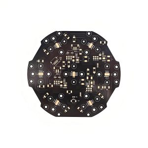
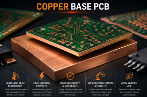
Copper base PCB materials are used for circuit boards that need strong thermal conductivity, high current capacity, mechanical stability, and reliable operation under heat stress. Compared with standard FR4 and aluminum-based boards, copper base PCBs provide better heat spreading because copper has excellent thermal and electrical performance. They are commonly used in power electronics, high-power LED modules, automotive lighting, charging systems, motor drives, industrial controls, and thermal management applications.

Copper Base PCB Materials

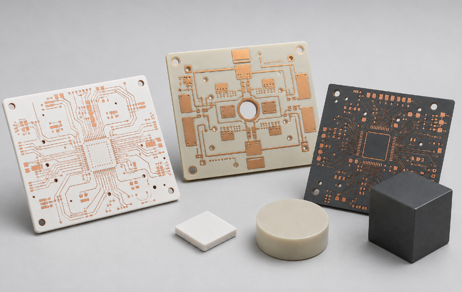
What Are Copper Base PCB Materials?

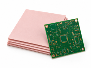
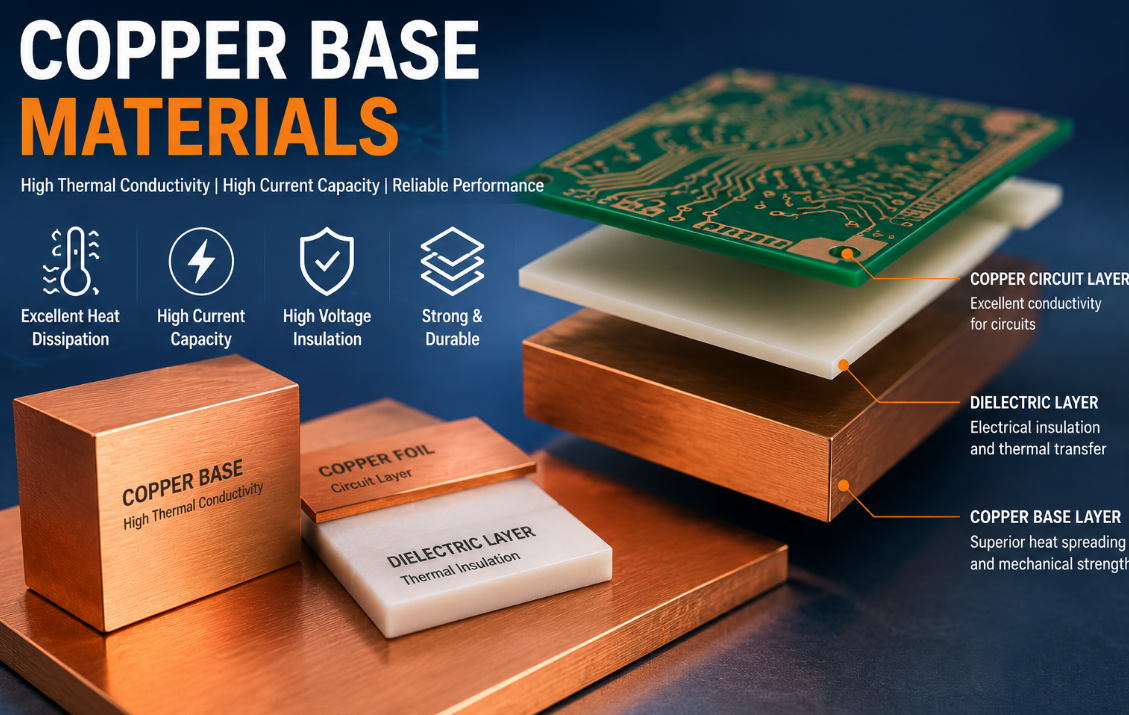
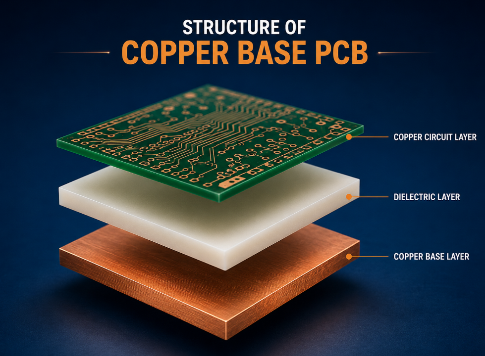
Copper base PCB materials refer to the material stack used to build a copper metal core PCB. A typical structure includes a copper circuit layer, a thermally conductive dielectric layer, and a copper base substrate. The copper circuit layer carries electrical signals or power, the dielectric layer provides insulation and heat transfer, and the copper base spreads heat away from components.

Unlike a standard FR4 PCB, a copper base PCB is designed mainly for thermal management and high-power reliability. The copper base acts as a strong heat spreader, helping reduce hot spots around LEDs, MOSFETs, IGBTs, power modules, and other heat-generating components.

For industrial projects, choosing the right copper base PCB materials affects thermal resistance, breakdown voltage, soldering reliability, board flatness, mechanical strength, surface finish quality, and long-term service life.

Why Are Copper Base PCB Materials Important?

Copper base PCB materials are important because high-power electronics often fail when heat cannot be removed fast enough. Excessive heat may cause component aging, solder joint fatigue, dielectric breakdown, copper delamination, unstable output, and reduced product lifetime.

Copper has better thermal conductivity than aluminum, which makes copper base PCBs useful when the design has higher heat density, smaller space, higher current, or stricter temperature limits. This is especially valuable for power modules, LED lighting, automotive electronics, and industrial power control systems.

In batch production, material consistency is also critical. A copper base PCB may look simple, but small differences in dielectric thickness, copper base quality, copper foil thickness, surface finish, and lamination control can affect real thermal performance.

How Do Copper Base PCB Materials Work?

Copper base PCB materials work by building a fast heat transfer path from the component to the copper base. Heat moves from the component pad into the copper circuit layer, passes through the thermally conductive dielectric layer, and spreads into the copper substrate.

The dielectric layer is the key bridge between electrical insulation and thermal transfer. It must isolate the copper circuit from the copper base while still allowing heat to pass efficiently. If the dielectric layer is too thick or has poor thermal conductivity, the board may not perform as expected.

The copper base then spreads heat across a larger area. This helps reduce local hot spots and supports better contact with a heatsink, metal housing, cooling plate, or thermal interface material. In real products, performance also depends on component layout, copper pad size, mounting pressure, solder quality, airflow, and enclosure design.

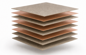
What Is the Structure of a Copper Base PCB?

A common copper base PCB has three main functional layers: copper circuit layer, dielectric insulation layer, and copper base layer. Some designs also include solder mask, surface finish, silkscreen, plated holes, and protective coating.

LayerMain FunctionKey Selection Points
Copper circuit layerCarries current and forms pads/tracesCopper thickness, trace width, current capacity
Dielectric layerProvides insulation and heat transferThermal conductivity, breakdown voltage, thickness
Copper base layerSpreads heat and supports the boardCopper grade, thickness, flatness, thermal performance
Solder maskProtects copper circuitsHeat resistance, adhesion, insulation, color
Surface finishProtects exposed copper padsSolderability, shelf life, assembly compatibility

For high-power products, the dielectric layer and copper base thickness are often the most important material choices. They directly affect heat flow, voltage safety, and long-term reliability.

copper base PCB structure

What Types of Copper Base PCB Materials Are Common?

Copper base PCB materials can be divided by structure, thermal performance, copper thickness, insulation type, and application requirement. The most common types include standard copper base materials, high thermal conductivity copper base materials, high-voltage insulation copper base materials, and heavy copper copper-base materials.

Standard copper base materials are used for power boards, LED modules, and industrial products that need better thermal performance than aluminum or FR4.

High thermal conductivity materials are used in compact power electronics, high-brightness LED modules, and products where heat concentration is severe.

High-voltage insulation materials are selected when the circuit must pass voltage withstand testing or operate under higher voltage stress.

Heavy copper copper-base materials are used for high-current circuits, power conversion, charging systems, motor drivers, and energy control products where both current and heat are major concerns.

What Copper Base Materials Are Used in Copper Base PCBs?

The copper base is usually made from high-purity copper or copper alloy depending on thermal performance, mechanical strength, machinability, and cost. Common choices include C1100 copper, C1020 oxygen-free copper, T2 copper, and selected copper alloys.

Copper Base TypeTypical FeaturesCommon Use
C1100 copperHigh thermal and electrical conductivityPower boards, LED thermal boards
C1020 oxygen-free copperHigh purity, stable conductivity, low oxygen contentHigh-reliability thermal applications
T2 copperGood conductivity, common industrial availabilityGeneral copper base PCB projects
Copper alloyBetter mechanical strength, lower conductivity than pure copperStructural or special mechanical applications

For most thermal PCB projects, the copper base is selected for heat spreading, flatness, thickness stability, machining quality, and bonding reliability. If the board must contact a heatsink or housing, surface flatness becomes especially important.

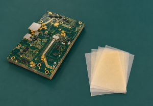
What Dielectric Materials Are Used in Copper Base PCB Materials?

The dielectric layer is usually a ceramic-filled thermally conductive polymer system. It must provide electrical insulation while transferring heat from the copper circuit layer to the copper base. This layer is often more important than the copper base itself because it controls the main thermal bottleneck.

Important dielectric properties include thermal conductivity, dielectric breakdown voltage, thickness, adhesion strength, glass transition temperature, thermal aging resistance, and moisture resistance.

Dielectric PropertyWhy It Matters
Thermal conductivityControls heat transfer from circuit layer to copper base
Dielectric strengthPrevents electrical breakdown between circuit and base
ThicknessAffects both heat transfer and insulation safety
Adhesion strengthReduces delamination risk during thermal cycling
Heat resistanceImproves reliability during soldering and operation
Moisture resistanceProtects insulation under humid conditions

A common selection mistake is focusing only on copper thickness while ignoring dielectric performance. In real operation, a poor dielectric layer can limit the full advantage of a copper base PCB.

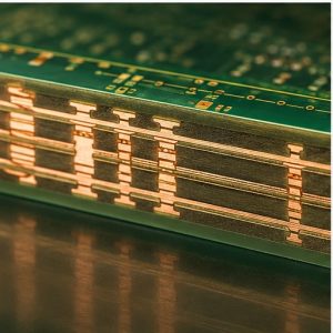
What Copper Thickness Is Used in Copper Base PCB Materials?

Copper thickness affects current capacity, heat spreading, etching accuracy, soldering performance, and cost. Common copper foil thicknesses include 1 oz, 2 oz, 3 oz, 4 oz, and heavier copper options. The copper base itself may be much thicker, often selected based on mechanical and thermal needs.

Copper ThicknessTypical UseKey Consideration
1 ozLED and general control circuitsGood for standard current and finer traces
2 ozPower supplies and LED driversBetter current capacity and heat spreading
3 oz to 4 ozHigh-current power boardsRequires wider spacing and stronger etching control
Heavy copperMotor drives, chargers, energy systemsHigher cost and more complex processing

For high-current designs, copper thickness should be selected together with trace width, temperature rise target, insulation distance, solder mask capability, and assembly process. More copper is helpful, but overusing heavy copper can increase cost and manufacturing difficulty.

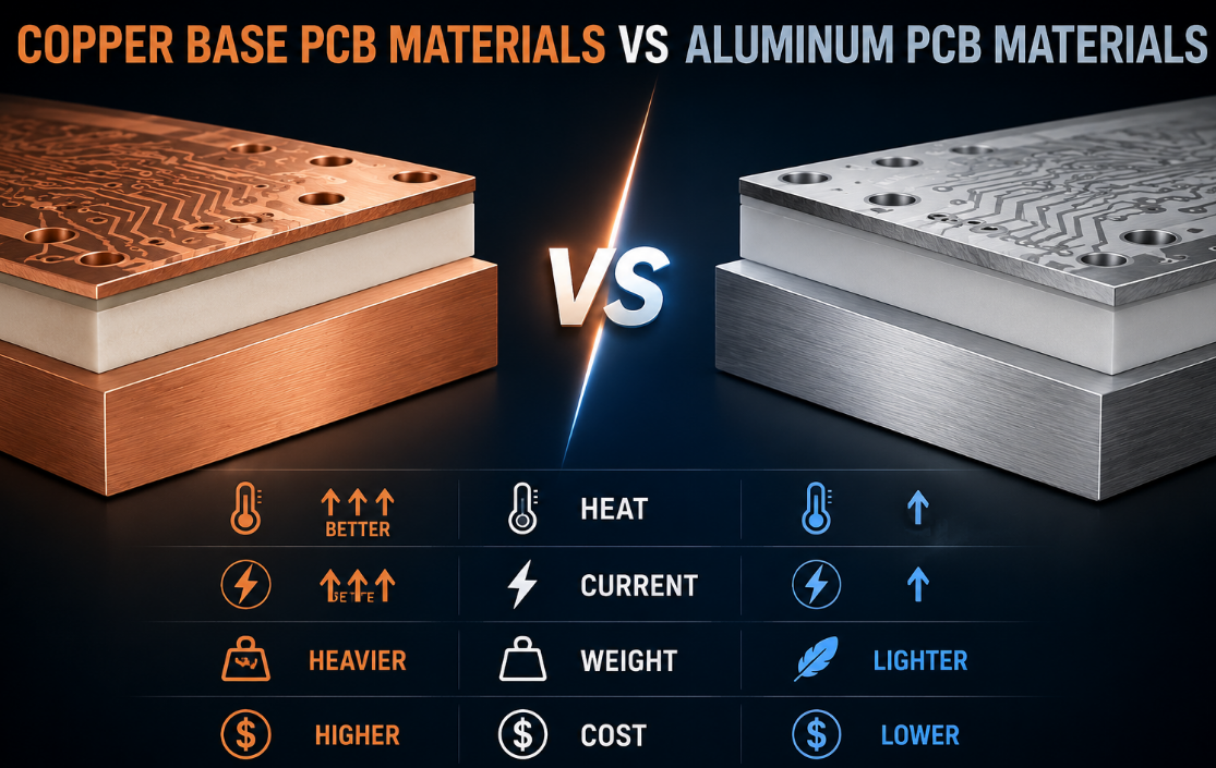
How Do Copper Base PCB Materials Compare with Aluminum PCB Materials?

Copper base PCB materials and aluminum PCB materials are both metal core solutions, but they are used for different thermal and cost targets.

Comparison ItemCopper Base PCB MaterialsAluminum PCB Materials
Thermal conductivityHigher heat spreading performanceGood but lower than copper
Current capacityBetter for high-current designsSuitable for many LED and power boards
Mechanical weightHeavierLighter
Material costHigherMore cost-effective
Machining difficultyMore demandingEasier and more common
Best useHigh-power, compact, high-heat productsLED lighting, general power products
Cost controlHigher project costBetter for budget-sensitive projects

Copper base PCB materials are usually chosen when heat density is too high for aluminum-based boards. Aluminum PCB materials are still a good choice when the project needs balanced performance and cost.

copper base PCB materials vs aluminum PCB materials

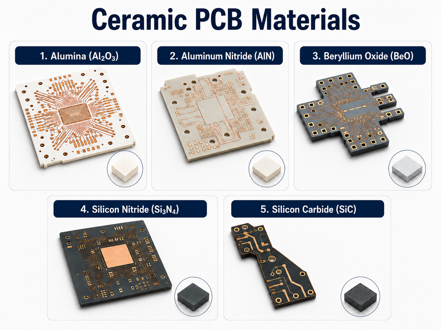
How Do Copper Base PCB Materials Compare with Ceramic PCB Materials?

Copper base PCBs and ceramic PCBs are both used for thermal applications, but their material behavior is different. Copper base boards provide excellent heat spreading and mechanical toughness, while ceramic boards provide strong insulation and high thermal stability.

Comparison ItemCopper Base PCB MaterialsCeramic PCB Materials
Heat spreadingExcellent through copper baseExcellent through ceramic substrate
Electrical insulationDepends on dielectric layerCeramic itself provides insulation
Mechanical behaviorTough and metallicHard but brittle
CostUsually high but practical for many power boardsOften higher for advanced ceramics
Current handlingStrong for high-current circuitsDepends on metallization and structure
Best usePower, LED, automotive, industrial controlRF, laser, medical, aerospace, power modules

Copper base PCBs are often selected when the project needs high thermal spreading, high current, mechanical durability, and practical assembly compatibility. Ceramic PCBs are selected when insulation stability, low expansion, or advanced thermal performance is more critical.

What Thermal Conductivity Is Needed for Copper Base PCB Materials?

The required thermal conductivity depends on component power, temperature limit, board size, copper area, dielectric thickness, cooling method, and operating environment. Copper itself has very high thermal conductivity, but the final PCB performance depends heavily on the dielectric layer.

For many copper base PCB designs, the dielectric layer is the main thermal bottleneck. A thinner high-performance dielectric can improve heat transfer, but it must still meet voltage and insulation requirements.

The better way to select materials is to evaluate total thermal resistance, not only the thermal conductivity of one layer. The full stack-up, component layout, soldering quality, contact surface, and heatsink design all influence the final temperature.

What Electrical Properties Should Be Checked?

Copper base PCB materials must provide reliable current carrying ability and electrical insulation. Because the copper base is conductive, the dielectric layer must safely isolate the circuit layer from the metal substrate.

Important electrical properties include breakdown voltage, insulation resistance, creepage and clearance distance, copper thickness, current capacity, leakage risk, and voltage withstand testing performance.

Electrical PropertyWhy It Matters
Breakdown voltagePrevents insulation failure between circuit and copper base
Insulation resistanceReduces leakage current risk
Copper thicknessSupports current carrying capacity
Creepage and clearanceImproves safety for high-voltage designs
Hi-pot performanceConfirms insulation reliability before shipment
Surface finish qualitySupports stable soldering and electrical contact

A copper base PCB can conduct heat very well, but it can fail if the insulation system is not suitable. For high-power designs, thermal and electrical requirements must be reviewed together.

What Surface Finishes Are Used with Copper Base PCB Materials?

Surface finish protects exposed copper pads and supports soldering. Common surface finishes include HASL, lead-free HASL, ENIG, OSP, immersion tin, and immersion silver. The right choice depends on component type, pad flatness, shelf life, soldering process, and cost.

Surface FinishAdvantagesCommon Use
HASLCost-effective and widely usedGeneral power and LED boards
Lead-free HASLRoHS-friendly solderabilityExport and compliant products
ENIGFlat surface, good shelf life, stable solderingPrecision assembly and high-reliability boards
OSPClean and economicalShort storage and fast assembly
Immersion tinGood flatness and solderabilitySelected power and connector designs
Immersion silverGood conductivity and solderabilityHigh-performance applications

For copper base boards with high current or high power density, surface finish should be selected with assembly reliability in mind. ENIG is often preferred for flatness and stable solder joints, while HASL may be used for cost-sensitive projects.

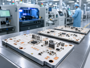
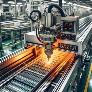
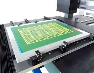
What Manufacturing Processes Are Used for Copper Base PCBs?

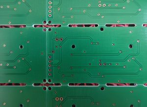
Copper base PCB manufacturing includes material preparation, drilling, imaging, etching, lamination, solder mask printing, surface finishing, profiling, testing, and final inspection. Compared with standard FR4 or aluminum PCBs, copper base PCBs require stronger process control because copper is heavier, softer, more conductive, and more demanding to machine.

Common production steps include cutting copper-clad laminate, drilling mounting holes, forming copper circuits, applying solder mask, processing surface finish, routing board outline, testing insulation, checking flatness, and inspecting appearance.

For thicker copper bases, drilling and profiling quality are especially important. Burrs, scratches, poor bonding, or dielectric damage can affect assembly, insulation, and thermal contact.

What Quality Tests Are Needed for Copper Base PCB Materials?

Copper base PCB materials should be tested for thermal, electrical, mechanical, and assembly reliability. Quality inspection should not only check whether the circuit is open or short. It should also confirm insulation strength, material bonding, flatness, and surface quality.

Test ItemPurpose
Visual inspectionChecks scratches, stains, solder mask defects, and exposed copper
Dimensional inspectionConfirms outline, hole size, thickness, and tolerance
Electrical testVerifies circuit continuity and isolation
Hi-pot testChecks dielectric withstand voltage
Insulation resistance testConfirms electrical isolation stability
Peel strength testChecks copper adhesion and bonding reliability
Flatness inspectionSupports heatsink contact and assembly fit
Thermal cyclingEvaluates material reliability under repeated heating and cooling

For high-power products, thermal testing after assembly is also helpful. Real load testing can reveal whether the selected material stack and cooling design are suitable.

What Common Problems Happen with Copper Base PCB Materials?

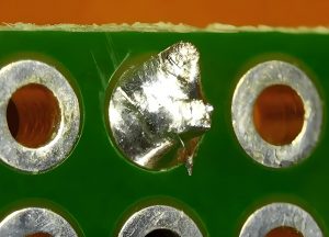
Common problems include poor insulation, dielectric breakdown, delamination, board warpage, copper burrs, poor solderability, weak bonding, scratches on copper base, and unstable thermal contact.

Poor insulation may happen if the dielectric layer is too thin, damaged, or unsuitable for the voltage requirement. Delamination may result from weak adhesion, poor lamination, moisture stress, or severe thermal cycling. Burrs around copper edges may affect assembly safety and insulation clearance.

Many failures are caused by the combination of wrong material selection, aggressive thermal load, poor mechanical mounting, unsuitable surface finish, and weak process control. For high-power products, material selection should be verified during prototype testing before full production.

How to Choose the Right Copper Base PCB Materials?

Choosing the right copper base PCB materials starts with the real application. Confirm power level, current load, operating voltage, maximum temperature, board size, component layout, cooling method, insulation requirement, and assembly process.

For LED modules, focus on thermal conductivity, surface reflectivity, dielectric stability, and soldering reliability. For power electronics, focus on copper thickness, current capacity, insulation strength, thermal resistance, and heat cycling reliability. For automotive and industrial applications, focus on temperature cycling, vibration resistance, corrosion protection, and batch consistency.

The best material is not always the most expensive material. The right material is the one that meets thermal, electrical, mechanical, cost, and production requirements at the same time.

What Factors Affect the Cost of Copper Base PCB Materials?

Copper base PCBs are usually more expensive than aluminum PCBs because copper material cost is higher and processing is more demanding. Cost depends on copper base thickness, copper foil thickness, dielectric thermal conductivity, dielectric thickness, surface finish, board size, tolerance, test requirements, and order quantity.

Cost FactorWhy It Affects PriceCost Control Suggestion
Copper base thicknessMore copper increases material costUse thickness based on real thermal need
Heavy copper circuitsRequires more material and process controlMatch copper thickness to current demand
Dielectric gradeHigher thermal and voltage performance costs moreChoose according to real application stress
Surface finishENIG and special finishes cost moreSelect based on assembly and reliability needs
Board outlineComplex routing increases machining timeSimplify unnecessary shapes
TestingHi-pot, thermal cycling, and special tests add costApply critical tests where required
QuantitySmall batches have higher setup costPlan prototype and batch production together

A low-cost material may create higher total cost if it causes overheating, insulation failure, rework, or field complaints. Cost control should focus on safe optimization, not material downgrading.

Where Are Copper Base PCB Materials Commonly Used?

Copper base PCB materials are used in products that require high thermal performance, high current capacity, and reliable long-term operation.

High-power LED lighting: industrial lights, automotive lights, stage lights, UV LED modules, and compact lighting systems.

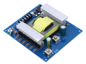
Power electronics: converters, inverters, power supplies, regulators, charging modules, and MOSFET power boards.

Automotive electronics: headlights, battery control units, charging systems, power distribution boards, and thermal control modules.

Industrial control: motor drives, automation modules, high-current control boards, and machine electronics.

Energy systems: solar inverters, battery packs, energy storage equipment, and charging stations.

Thermal management modules: compact designs where heat must move quickly from the circuit to a metal body or heatsink.

What Should You Confirm Before Ordering Copper Base PCBs?

Before ordering copper base PCBs, confirm copper base thickness, copper foil thickness, dielectric thermal conductivity, dielectric thickness, voltage requirement, operating temperature, surface finish, solder mask color, board outline, tolerance, and inspection standard.

You should also provide complete production files, including Gerber files, drill files, stack-up notes, drawings, material requirements, quantity, surface finish, testing requirements, and application details. For assembly projects, BOM and placement files should also be provided.

For high-power or high-voltage projects, prototype validation is strongly recommended. Testing the board under real load helps confirm whether the material stack, heat path, and mechanical mounting design are suitable before batch production.

Why Choose EBest for Copper Base PCB Manufacturing?

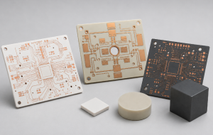
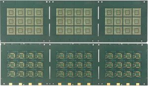
EBest Technology provides one-stop PCB solutions, including PCB design, PCB prototype, mass production, component sourcing, PCB assembly, and box-build assembly. Its product range includes standard FR4 PCB, multilayer PCB, metal-based PCB, ceramic PCB, flexible PCB, rigid-flex PCB, and high frequency PCB, supporting customers with different electronic manufacturing needs.

For copper base PCB projects, EBest can support engineering review, material selection, prototype validation, batch production, assembly coordination, quality inspection, and global delivery. This is useful when a project involves high-power components, thermal design, mechanical housings, connectors, and final product assembly.

EBest also supports quality and compliance systems such as IATF 16949, ISO 9001:2015, ISO 13485:2016, AS9100D, REACH, RoHS, and UL-related requirements. These capabilities help customers manage industrial, automotive, medical, aerospace, and export-oriented projects with more confidence.

copper base PCB

FAQs About Copper Base PCB Materials

Q1: What are copper base PCB materials made of?
A1: Copper Base PCB Materials usually include a copper circuit layer, a thermally conductive dielectric layer, and a copper base substrate. The copper circuit carries current, the dielectric provides insulation and heat transfer, and the copper base spreads heat away from components.

Q2: Why use copper base PCB materials instead of aluminum PCB materials?
A2: Copper base PCB materials are used when a project needs higher thermal spreading, higher current capacity, and stronger heat control than aluminum PCBs can provide. They are common in high-power LED, power electronics, automotive lighting, and industrial control products.

Q3: What is the most important layer in a copper base PCB?
A3: The dielectric layer is often the most critical because it controls both insulation safety and heat transfer. Even with a strong copper base, poor dielectric performance can cause overheating, electrical breakdown, or delamination during long-term operation.

Q4: What copper thickness should I choose for a copper base PCB?
A4: The right copper thickness depends on current load, trace width, temperature rise, and board size. Standard designs may use 1 oz or 2 oz copper, while power boards may require 3 oz, 4 oz, or heavier copper for better current capacity.

Q5: Are copper base PCBs suitable for high-voltage applications?
A5: Yes, but the dielectric layer must have enough breakdown voltage, insulation resistance, and creepage clearance. High-voltage designs should define operating voltage, surge voltage, test voltage, and safety requirements before material selection.

Q6: Are copper base PCBs more expensive than aluminum PCBs?
A6: Yes. Copper base PCBs usually cost more because copper material is more expensive and processing is more demanding. They are usually selected when the project needs higher thermal performance or higher current capability that justifies the cost.

Q7: Can copper base PCB materials be used for LED lighting?
A7: Yes. Copper base PCB materials are suitable for high-power LED lighting, especially when LED density is high or the product has limited cooling space. They help reduce hot spots and support brightness stability and longer service life.

Q8: What surface finish is recommended for copper base PCBs?
A8: Common options include HASL, lead-free HASL, ENIG, OSP, immersion tin, and immersion silver. ENIG is often selected for flat pads, better shelf life, and stable soldering, while HASL may be used for cost-sensitive designs.

Q9: Why do copper base PCBs delaminate?
A9: Delamination may happen because of weak bonding, poor dielectric material, moisture stress, high soldering temperature, or repeated thermal cycling. Proper material selection, lamination control, and thermal design help reduce this risk.

Q10: What tests are needed for copper base PCBs?
A10: Important tests include electrical test, hi-pot test, insulation resistance test, dimensional inspection, visual inspection, peel strength test, flatness inspection, and thermal cycling. For high-power boards, real load thermal testing is also recommended.

Q11: Can copper base PCBs support PCB assembly?
A11: Yes. Copper base PCBs can support SMT assembly and selected through-hole assembly, depending on design structure. Assembly planning should consider heat absorption, soldering profile, component placement, surface finish, and board flatness.

Q12: What files are needed for a copper base PCB quotation?
A12: Provide Gerber files, drill files, copper thickness, copper base thickness, dielectric requirements, surface finish, solder mask color, board thickness, quantity, drawings, voltage requirement, and application details. For assembly, also provide BOM and placement files.

Conclusion

Copper base PCB materials are used when a circuit board needs strong heat spreading, high current capacity, reliable insulation, and stable long-term performance. The key is not only choosing a copper base, but also selecting the right dielectric layer, copper foil thickness, surface finish, and testing requirements.

For engineering projects, do not choose materials by thermal conductivity alone. Review thermal resistance, voltage safety, current load, mounting method, operating environment, and production consistency before confirming the stack-up. For procurement, work with a manufacturer that can support material review, prototype testing, batch control, assembly coordination, and reliable delivery.

If you need copper base PCB materials , copper base PCB manufacturing, PCB assembly, OEM production, ODM development, sample testing, batch production, or custom engineering solutions, please contact our team at sales@bestpcbs.com for technical support and quotation service.

You may also like

Rigid-Flex PCB Materials
Tuesday, June 2nd, 2026


Need reliable Rigid-Flex PCB Materials for compact electronics? Learn material types, stack-up choices, bend reliability, cost factors and supplier selection.

What Are Rigid-Flex PCB Materials?

Rigid-Flex PCB Materials are the combined material systems used to build circuit boards with both rigid sections and flexible bending sections. These materials usually include rigid laminate, flexible polyimide film, copper foil, adhesive or adhesiveless flexible copper-clad laminate, prepreg, coverlay, bonding film and surface finish.

A rigid-flex PCB is not simply a rigid board connected to a flex cable. It is an integrated circuit structure where the flexible layers usually pass through or connect between rigid areas. This design helps reduce connectors, save internal space and improve long-term reliability in compact electronic products.

The material choice directly affects bending life, signal stability, heat resistance, copper adhesion, layer bonding and final assembly yield. If the wrong material is selected, the board may crack, delaminate, lose impedance control or fail during repeated bending.

Rigid-Flex PCB Materials, https://www.bestpcbs.com/blog/2026/06/rigid-flex-pcb-materials/

Why Are Rigid-Flex PCB Materials Important?

Rigid-flex PCB materials are important because they decide whether the board can survive both mechanical movement and electrical operation. A rigid-flex design often appears in devices where space is limited, wiring must bend and long-term reliability is required.

Common applications include medical devices, aerospace electronics, automotive modules, cameras, wearables, industrial sensors and portable electronics. These products often need smaller size, lighter weight and fewer connector points.

Industry guidance commonly refers to IPC-2223 for flexible and rigid-flex board design. IPC-2223 is a sectional design standard for flexible and rigid-flex printed boards, and it is often used together with qualification and performance standards for flex circuits.

For buyers, the material choice affects not only board price but also field reliability. A low-cost material stack-up may look acceptable at the quotation stage, but it can create hidden risks during bending, assembly or long-term thermal cycling.

How Do Rigid-Flex PCB Materials Work?

Rigid-flex PCB materials work by combining stable rigid areas with bendable flexible areas in one continuous circuit structure. The rigid parts support components, solder joints and mechanical assembly. The flexible parts allow folding, bending or connection between product sections.

The flexible section usually uses polyimide film because it offers strong heat resistance, dimensional stability and bending performance. Copper traces are laminated or bonded to the polyimide, then protected by coverlay or flexible solder mask.

The rigid section usually uses FR4, high-Tg FR4, halogen-free laminate, polyimide rigid laminate or high-frequency laminate, depending on electrical, thermal and reliability needs. Prepreg or bonding film connects the rigid and flexible structures during lamination.

What Are the Main Materials Used in Rigid-Flex PCB?

The main rigid-flex PCB materials include polyimide film, copper foil, FR4 laminate, high-Tg laminate, prepreg, adhesive, coverlay, stiffener and surface finish materials. Each material has a different function in the final board.

MaterialFunctionCommon Selection Point
Polyimide FilmFlexible dielectric baseHeat resistance and bending life
Copper FoilConductive circuit layerRolled annealed or electrodeposited copper
FR4 LaminateRigid area supportCost, Tg, mechanical strength
High-Tg FR4Rigid area for thermal stressBetter heat resistance
Polyimide LaminateHigh-reliability rigid sectionAerospace and harsh environments
PrepregLayer bonding in rigid areaLamination compatibility
AdhesiveBonds copper and dielectricFlexibility and delamination risk
CoverlayProtects flex copper tracesBend durability and insulation
Flexible Solder MaskFine pattern protectionDetailed geometry
StiffenerReinforces connector or assembly areaPI, FR4 or stainless steel

The best material system should be selected based on bend type, assembly method, thermal condition, electrical requirement and product lifetime.

What Flexible Core Materials Are Used in Rigid-Flex PCB?

The most common flexible core material is polyimide, often called PI. Polyimide is widely used because it can tolerate high soldering temperatures, repeated bending and harsh operating environments.

Flexible copper-clad laminate can be adhesive-based or adhesiveless. Adhesive-based material uses an adhesive layer between copper and polyimide. Adhesiveless material bonds copper directly to the film without a separate adhesive interface.

Adhesiveless construction can reduce total thickness and remove one interface where fatigue or delamination may start. This makes it useful for thin, high-reliability or dynamic-flex designs.

For most rigid-flex projects, the flexible material must be chosen early because it affects bend radius, copper fatigue, stack-up thickness and final reliability testing.

What Rigid Materials Are Used in Rigid-Flex PCB?

The rigid area of a rigid-flex PCB usually uses FR4, high-Tg FR4, halogen-free FR4, polyimide laminate or high-frequency laminate. The choice depends on cost, temperature, signal speed and mechanical requirements.

Standard FR4 is suitable for many commercial products where cost control is important. High-Tg FR4 is better for products that face higher soldering temperature, thermal cycling or long-term heat exposure.

Polyimide rigid laminate is often used in aerospace, defense, medical and high-reliability products. It costs more than FR4 but offers stronger thermal stability and better reliability under demanding conditions.

For RF or high-speed designs, engineers may choose special low-loss laminates in the rigid section. In this case, material matching between rigid and flexible areas becomes more important because impedance and dimensional stability must be controlled.

What Is Coverlay in Rigid-Flex PCB Materials?

Coverlay is a protective layer used over flexible copper traces. It is usually made from polyimide film with adhesive, and it protects the circuit from moisture, abrasion, handling damage and electrical shorting.

Coverlay is different from standard rigid PCB solder mask. It is more flexible and better suited for bending areas. Common coverlay structures may use 12.5–50 μm polyimide film with 12.5–25 μm adhesive, depending on design needs.

Coverlay is usually preferred in high-flex or harsh-use areas. Flexible solder mask may be used when the design needs finer openings or more detailed geometry, but it may not provide the same mechanical protection in repeated bending areas.

What Copper Foil Is Best for Rigid-Flex PCB Materials?

Copper foil is one of the most important rigid-flex PCB materials because it carries current and also survives bending stress. The two common choices are rolled annealed copper and electrodeposited copper.

Rolled annealed copper is often preferred for dynamic bending because its grain structure supports better flex life. Electrodeposited copper is widely used in standard PCB production and can be suitable for static bending or bend-to-install applications.

For high-reliability flexible sections, copper thickness should not be selected only by current capacity. Thicker copper can carry more current, but it also increases bending stress. Engineers must balance current load, bend radius, flex cycle requirement and trace width.

What Is the Difference Between Adhesive and Adhesiveless Rigid-Flex Materials?

Adhesive rigid-flex materials use an adhesive layer to bond copper to polyimide. This structure is common, cost-effective and widely available. It is suitable for many static-flex and commercial rigid-flex products.

Adhesiveless rigid-flex materials do not use a separate adhesive layer between copper and polyimide. This creates a thinner structure and may improve bending reliability because there is one less interface that can fail.

Material TypeMain AdvantageMain LimitationBest Use
Adhesive-Based Flex MaterialLower cost and wide availabilityThicker structure, more delamination riskStatic flex, general electronics
Adhesiveless Flex MaterialThinner, better reliability, improved bend lifeHigher costDynamic flex, compact and high-reliability designs

If the product only bends during assembly, adhesive-based material may be enough. If the product bends repeatedly during use, adhesiveless material is often a better choice.

Adhesive and Adhesiveless Rigid-Flex Materials, https://www.bestpcbs.com/blog/2026/06/rigid-flex-pcb-materials/

How Should Rigid-Flex PCB Materials Be Selected for Bend Reliability?

Rigid-flex PCB materials should be selected according to whether the bend is static, dynamic or bend-to-install. Static bending means the board is bent once or rarely moved. Dynamic bending means the board bends repeatedly during product use.

For dynamic bending, engineers should prioritize thin polyimide, rolled annealed copper, adhesiveless construction, proper coverlay and controlled copper layout. The flex area should avoid sharp corners, plated holes, sudden width changes and unnecessary copper density.

For better bend reliability, flex layers are often kept to one or two layers when possible. This helps reduce material thickness, lower bending stress and improve mechanical flexibility.

Material selection and layout must work together. Even excellent material can fail if the bend radius is too small, copper traces cross the bend incorrectly or the transition area is poorly designed.

Rigid-Flex PCB Materials, https://www.bestpcbs.com/blog/2026/06/rigid-flex-pcb-materials/

How Do Rigid-Flex PCB Materials Affect Signal Integrity?

Rigid-flex PCB materials affect signal integrity through dielectric constant, dielectric thickness, copper roughness, trace geometry and layer transition design. For high-speed signals, uncontrolled material changes between rigid and flex areas can create impedance mismatch.

Polyimide usually has different electrical properties from FR4 or high-frequency rigid laminates. This means the stack-up must be reviewed carefully when controlled impedance is required.

For RF, antenna, camera module, high-speed data or medical signal applications, engineers should confirm Dk, Df, copper type, trace width, spacing, reference plane continuity and bend area routing. Material datasheets alone are not enough; the actual stack-up must be calculated and verified.

What Are Common Rigid-Flex PCB Material Failures?

Common material-related failures include copper cracking, coverlay separation, delamination, resin recession, rigid-flex transition cracking, solder joint fatigue, insulation failure and impedance drift. Many of these failures start from poor material matching or weak stack-up design.

Copper cracking often happens when copper is too thick, bend radius is too tight or trace direction is poorly arranged. Delamination may occur when adhesive systems, lamination settings or thermal cycling conditions are not properly controlled.

The rigid-flex transition area is especially important. This area connects a stiff rigid structure to a flexible structure, so stress can concentrate there. Material thickness, coverlay extension, copper layout and mechanical support must be designed carefully.

What Standards Apply to Rigid-Flex PCB Materials?

The most commonly referenced design standard is IPC-2223, which covers flexible and rigid-flex printed board design. Manufacturers and engineers may also refer to related IPC performance and qualification standards for flexible printed circuits.

IPC-related rigid-flex guidance is important because it helps define material use, stack-up design, bend reliability, coverlay rules and testing expectations. These standards help reduce design ambiguity between customers, PCB engineers and manufacturers.

For commercial projects, buyers may also request RoHS, REACH, UL, ISO quality management, halogen-free material or automotive reliability documentation depending on the final market.

Where Are Rigid-Flex PCB Materials Used?

Rigid-flex PCB materials are used in electronic products that require compact assembly, folding structure, lightweight design and reliable interconnection. Common industries include medical electronics, aerospace, automotive, industrial control, robotics, consumer electronics, wearables and communication devices.

Typical applications include camera modules, surgical tools, hearing aids, wearable sensors, automotive control modules, UAV electronics, display modules, foldable devices, test equipment and compact power systems.

Rigid-flex boards are especially useful when connectors and wire harnesses create space, weight or reliability problems. By replacing separate cables and connectors, rigid-flex PCB materials can help simplify assembly and reduce failure points.

Rigid-Flex PCB Materials Application, https://www.bestpcbs.com/blog/2026/06/rigid-flex-pcb-materials/

How Do Rigid-Flex PCB Materials Affect Cost?

Rigid-flex PCB materials affect cost through material grade, layer count, flex layer number, copper thickness, coverlay type, adhesive type, rigid laminate type, controlled impedance needs and testing requirements.

Adhesiveless materials, high-Tg laminates, polyimide rigid laminates, low-loss materials and dynamic-flex structures usually cost more. However, they may reduce connector cost, assembly labor, field failure and product size.

Cost should be evaluated at the product level. A rigid-flex PCB may have a higher board price than a separate rigid PCB and flex cable, but it can reduce assembly steps, connector quantity, internal space and long-term reliability risk.

How Can Buyers Choose a Rigid-Flex PCB Materials Supplier?

Buyers should choose a supplier that understands both rigid PCB manufacturing and flexible circuit behavior. Rigid-flex production requires control of lamination, coverlay alignment, bend area stress, copper adhesion and dimensional stability.

A good supplier should provide material stack-up review, DFM feedback, impedance support, prototype validation, quality inspection and mass production control. The supplier should also help confirm bend radius, copper type, coverlay design and rigid-flex transition structure before production.

For OEM and ODM projects, buyers should not only compare price. They should ask whether the factory has experience with similar products, similar layer counts and similar reliability requirements.

What Should You Confirm Before Ordering Rigid-Flex PCB Materials?

Before ordering rigid-flex PCB materials, confirm the rigid laminate, flexible core material, copper type, copper thickness, adhesive or adhesiveless structure, coverlay thickness, stack-up, bend radius and surface finish.

You should also confirm whether the board is static-flex or dynamic-flex. This single detail can change the material recommendation, copper choice and bend design rules.

For production preparation, provide Gerber files, stack-up requirements, assembly drawing, bend direction, bend radius, component height limits, impedance needs and final application environment. This helps the manufacturer identify risks before tooling and lamination.

FAQs About Rigid-Flex PCB Materials

Q1: What are the most common Rigid-Flex PCB Materials?
A1: The most common Rigid-Flex PCB Materials include polyimide film, copper foil, FR4 laminate, high-Tg FR4, prepreg, adhesive, coverlay, flexible solder mask and stiffener materials. Polyimide is used in the flexible area, while FR4 or high-Tg laminate is often used in the rigid area.

Q2: Why is polyimide used in rigid-flex PCB materials?
A2: Polyimide is used because it provides strong heat resistance, flexibility and dimensional stability. It can survive soldering temperature and repeated bending better than many organic materials. This makes it suitable for flexible sections in medical devices, automotive modules, aerospace products and compact electronics.

Q3: Is adhesiveless material better for rigid-flex PCB?
A3: Adhesiveless material is often better for thin, high-reliability or dynamic-flex designs because it removes one adhesive interface and can improve bending performance. However, it costs more than adhesive-based material. For static flex or bend-to-install products, adhesive-based materials may still be practical and cost-effective.

Q4: What copper is best for flexible areas?
A4: Rolled annealed copper is usually preferred for flexible areas that need repeated bending because it has better fatigue resistance. Electrodeposited copper can be suitable for static bend or standard applications. The best choice depends on flex cycle requirement, copper thickness, bend radius and current load.

Q5: What is coverlay in rigid-flex PCB materials?
A5: Coverlay is a protective polyimide-based layer used over copper traces in the flexible area. Common coverlay materials may use 12.5–50 μm polyimide film and 12.5–25 μm adhesive. It protects the circuit from abrasion, moisture and electrical shorting, especially in bend areas.

Q6: Can rigid-flex PCB materials support controlled impedance?
A6: Yes, rigid-flex PCB materials can support controlled impedance, but the stack-up must be carefully designed. Engineers should control Dk, Df, trace width, dielectric thickness, copper roughness and reference plane continuity. This is especially important for RF, camera, antenna and high-speed data applications.

Q7: What causes rigid-flex PCB material failure?
A7: Common causes include tight bend radius, thick copper in bend areas, poor coverlay design, weak lamination, incorrect adhesive selection and stress concentration at the rigid-flex transition. Failures may appear as copper cracking, delamination, coverlay lifting, insulation problems or solder joint fatigue.

Q8: Are rigid-flex PCB materials expensive?
A8: Rigid-flex PCB materials are usually more expensive than standard rigid PCB materials because they combine rigid and flexible structures. Cost increases with layer count, flex layer number, adhesiveless material, controlled impedance and reliability testing. However, they can reduce connectors, labor and field failure risk.

Q9: What standards are used for rigid-flex PCB design?
A9: IPC-2223 is commonly referenced for flexible and rigid-flex printed board design. Depending on the product, buyers may also request IPC performance standards, RoHS, REACH, UL, ISO quality control or automotive reliability documentation. Standards help improve design consistency and production quality.

Q10: How do I choose materials for dynamic-flex applications?
A10: For dynamic-flex applications, choose thin polyimide, rolled annealed copper, suitable coverlay and preferably adhesiveless flexible copper-clad laminate. Keep the flex layer count low, often one or two layers when possible, avoid vias in bend areas and maintain a proper bend radius.

Q11: Can FR4 be used in rigid-flex PCB materials?
A11: Yes, FR4 is commonly used in the rigid sections of rigid-flex PCBs. For higher temperature or reliability needs, high-Tg FR4 or polyimide laminate may be selected. The flexible section usually uses polyimide, so the full stack-up must be reviewed for lamination compatibility and reliability.

Q12: What should buyers ask before ordering rigid-flex PCB materials?
A12: Buyers should ask about stack-up, flexible core material, copper type, coverlay thickness, bend radius, adhesive or adhesiveless construction, surface finish and testing plan. They should also confirm whether the supplier has experience with similar rigid-flex structures and can provide DFM support before production.

Conclusion

Rigid-Flex PCB Materials should be selected by matching the product’s mechanical movement, thermal condition, electrical requirement and assembly structure. Polyimide, copper foil, coverlay, adhesive system, rigid laminate and prepreg all affect the final reliability of the board.

For stable projects, focus on bend type, copper selection, stack-up balance, coverlay design, rigid-flex transition control and supplier capability. For procurement, the best choice is not always the lowest quote, but the material system that can support prototype validation, mass production and long-term product reliability.

You may also like

Ceramic PCB Materials
Tuesday, June 2nd, 2026

What are ceramic PCB materials and how do they affect heat, insulation and reliability? Learn Al2O3, AlN, BeO, Si3N4 selection, applications and buying tips.

What Are Ceramic PCB Materials?

Ceramic PCB materials are inorganic ceramic substrates used as the base of printed circuit boards instead of traditional organic materials such as FR4. They are selected when a circuit must handle high heat, high voltage, high frequency, or harsh operating environments.

Common ceramic PCB materials include alumina (Al2O3), aluminum nitride (AlN), beryllium oxide (BeO), silicon nitride (Si3N4), and sometimes silicon carbide (SiC). These materials provide strong electrical insulation while allowing heat to move away from power devices, LEDs, RF modules, and semiconductor components.

Unlike FR4, ceramic substrates do not mainly rely on glass fiber and epoxy resin. Their performance comes from the ceramic body itself, which offers better thermal conductivity, lower thermal expansion, stronger dimensional stability, and better resistance to high-temperature operation.

For engineers and buyers, the key point is simple: ceramic PCB material is not chosen only by price. It must match heat load, circuit voltage, mechanical stress, copper thickness, assembly process, and long-term reliability requirements.

Ceramic PCB Materials, https://www.bestpcbs.com/blog/2026/06/ceramic-pcb-materials/

Why Are Ceramic PCB Materials Important?

Ceramic PCB materials are important because modern electronic products generate more heat in smaller spaces. Power modules, high-brightness LEDs, EV electronics, RF amplifiers, laser devices, and semiconductor packages all need stable heat dissipation.

FR4 is suitable for many standard electronics, but its thermal conductivity is much lower than ceramic materials. Ceramic substrates can conduct heat far more effectively while still maintaining electrical insulation, which makes them valuable in circuits where heat cannot be allowed to accumulate around chips or solder joints.

Material choice also affects reliability. If the coefficient of thermal expansion does not match the component or copper layer, repeated heating and cooling may cause cracks, delamination, solder fatigue, or broken traces. In high-power products, this is often more serious than the initial material cost.

For procurement teams, ceramic PCB materials directly influence cost, lead time, processing difficulty, and supplier capability. A low-cost ceramic material may be enough for LED lighting, while an EV power module or high-frequency device may require AlN or another advanced ceramic substrate.

How Do Ceramic PCB Materials Work?

Ceramic PCB materials work by combining electrical insulation with thermal conduction. Most metals conduct heat well but also conduct electricity. Ceramics are different because they can transfer heat while resisting electrical current, allowing circuits to stay electrically isolated.

When a chip, LED, MOSFET, IGBT, or RF component generates heat, the ceramic substrate spreads that heat away from the component area. The heat can then move into copper layers, metal bases, housings, heat sinks, or cooling systems. This reduces hot spots and helps the device maintain stable performance.

The material structure also supports dimensional stability. Ceramic substrates usually have lower expansion than many organic PCB materials. This helps reduce mechanical stress in applications where devices repeatedly heat up and cool down.

In practical manufacturing, ceramic PCB performance depends not only on the ceramic base. It also depends on metallization, copper bonding, surface finish, drilling quality, laser processing, conductor adhesion, and assembly control.

What Are the Main Types of Ceramic PCB Materials?

The main ceramic PCB materials include Al2O3, AlN, BeO, Si3N4, and SiC. Each material has a different balance of heat dissipation, insulation, strength, safety, cost, and manufacturability.

Ceramic PCB MaterialMain StrengthTypical UseSelection Note
Alumina (Al2O3)Cost-effective, stable, widely availableLEDs, sensors, power circuits, industrial electronicsGood general-purpose ceramic PCB material
Aluminum Nitride (AlN)High thermal conductivity, good insulationPower modules, semiconductor devices, RF, high-power LEDsBetter for demanding thermal management
Beryllium Oxide (BeO)Very high thermal conductivitySpecial high-power and RF applicationsRestricted by toxicity concerns during processing
Silicon Nitride (Si3N4)Strong mechanical toughness, thermal shock resistanceAutomotive, power modules, harsh environmentsUseful where mechanical reliability matters
Silicon Carbide (SiC)High-temperature capability, strong hardnessExtreme environment electronicsLess common for standard ceramic PCBs
Ceramic PCB Materials Types, https://www.bestpcbs.com/blog/2026/06/ceramic-pcb-materials/

Alumina and aluminum nitride are the most common choices in many commercial ceramic PCB projects. Alumina is often selected when cost and stability matter most. Aluminum nitride is selected when high heat dissipation is the main requirement.

BeO can offer excellent thermal performance, but it requires strict safety control because of toxicity risk during machining. Many projects now prefer AlN as a safer alternative when high thermal conductivity and electrical insulation are needed.

What Is Alumina Ceramic PCB Material?

Alumina ceramic PCB material, also called Al2O3 ceramic substrate, is one of the most widely used ceramic PCB materials. It offers good electrical insulation, stable mechanical performance, high-temperature resistance, and lower cost compared with many advanced ceramic substrates.

Common alumina purity levels include 96% alumina and 99.6% alumina. A 96% alumina substrate is often used for cost-sensitive ceramic PCB applications, while 99.6% alumina may be selected when better surface quality, insulation, or stability is required.

Alumina thermal conductivity is lower than AlN but still much higher than standard FR4. Many alumina ceramic substrates are commonly used in the 24–30 W/m·K thermal conductivity range, depending on purity, formulation, and processing.

Alumina ceramic PCBs are commonly used in LED modules, sensors, automotive electronics, industrial controllers, thick-film circuits, power resistors, and compact electronic modules. For many buyers, alumina is the best balance between performance, price, and production availability.

What Is Aluminum Nitride Ceramic PCB Material?

Aluminum nitride ceramic PCB material, also called AlN ceramic substrate, is selected for high thermal conductivity and electrical insulation. It is widely used in high-power electronics, semiconductor packaging, laser modules, RF devices, EV power systems, and high-brightness LED applications.

AlN is valuable because its thermal conductivity is much higher than alumina. Many commercial AlN ceramic substrates are commonly listed around 150–220 W/m·K, while actual values depend on material grade and processing quality.

Another advantage is its thermal expansion behavior. AlN has a coefficient of thermal expansion closer to silicon than many other materials, which can help reduce thermal mismatch in semiconductor-related assemblies.

The main limitation is cost. AlN is usually more expensive than alumina and may require more careful process control. However, when thermal failure risk is high, the higher material cost can be justified by better reliability and longer product life.

What Is Beryllium Oxide Ceramic PCB Material?

Beryllium oxide, or BeO, is a ceramic material known for very high thermal conductivity and good electrical insulation. It has been used in some RF, microwave, aerospace, and high-power electronic applications where heat dissipation is extremely important.

Some BeO materials can offer very strong thermal performance, which makes them attractive for demanding thermal designs. However, BeO has a major safety concern because toxic dust can be produced during machining or improper processing.

Because of this risk, many companies avoid BeO unless the application truly requires it and the supplier has proper safety systems. For many modern projects, AlN is often considered a safer alternative.

Buyers should confirm safety compliance, handling documentation, machining control, and processing capability before choosing BeO for any ceramic PCB project.

What Is Silicon Nitride Ceramic PCB Material?

Silicon nitride, or Si3N4, is a ceramic material known for high mechanical strength, fracture toughness, and thermal shock resistance. It is valuable in harsh applications where cracking risk is a major concern.

Si3N4 is often considered when the circuit must survive mechanical stress, vibration, impact, or rapid temperature cycling. This makes it attractive for automotive power modules, industrial systems, transportation electronics, and high-reliability environments.

Compared with AlN, silicon nitride may not always provide the same level of thermal conductivity. Its advantage is mechanical robustness rather than only heat dissipation.

The practical choice depends on the full design. If the biggest risk is heat, AlN may be better. If the biggest risk is mechanical stress and thermal cycling, Si3N4 may deserve serious evaluation.

How Do Alumina, AlN, BeO and Si3N4 Compare?

Different ceramic PCB materials should be compared by application needs, not by a single performance number. Thermal conductivity is important, but it is not the only selection factor.

ItemAlumina Al2O3Aluminum Nitride AlNBeryllium Oxide BeOSilicon Nitride Si3N4
Thermal conductivityMediumHighVery highMedium to high
Electrical insulationHighHighHighHigh
Mechanical toughnessMediumMediumMediumHigh
Thermal shock resistanceGoodGoodGoodExcellent
Cost levelLowerHigherHigherHigher
Processing safetyGoodGoodSpecial control neededGood
Common availabilityVery highHighLimitedMedium
Best fitGeneral ceramic PCBHigh-power thermal designSpecial high-thermal projectsHarsh mechanical environments

For most commercial projects, alumina is the practical starting point and AlN is the upgrade path for higher thermal demand. BeO is a special-case material, while Si3N4 is often chosen for strength and thermal cycling resistance.

A good supplier should not recommend the most expensive material first. The better approach is to review power density, operating temperature, copper thickness, board size, assembly method, and reliability target before confirming the substrate.

What Properties Should You Check Before Selecting Ceramic PCB Materials?

Before selecting ceramic PCB materials, engineers should check thermal, electrical, mechanical, and manufacturing parameters. These properties determine whether the substrate can survive real operating conditions.

ParameterWhy It MattersTypical Selection Focus
Thermal conductivityControls heat dissipationHigher for power modules, LEDs, RF power devices
Dielectric strengthPrevents electrical breakdownImportant for high-voltage circuits
Dielectric constantAffects signal behaviorImportant for RF and high-frequency designs
Dissipation factorAffects signal lossLower is better for RF and microwave use
Coefficient of thermal expansionControls thermal stressMust match chips, copper, and package materials
Flexural strengthAffects breakage riskImportant for handling and assembly
Surface roughnessAffects metallization and bondingImportant for fine circuits and thin film processes
Copper adhesionAffects reliabilityCritical for DBC, DPC, thick copper, and power cycling
Substrate thicknessAffects strength and thermal pathMust balance insulation, rigidity, and heat transfer
Manufacturing toleranceAffects assembly fitImportant for precision modules

For high-power applications, thermal conductivity and copper adhesion are often the first concerns. For RF applications, dielectric constant, loss tangent, and surface quality become more important.

For procurement, the most common mistake is comparing only unit price. A cheaper substrate can become expensive if it causes cracking, poor yield, solder defects, or field failure after mass production.

What Ceramic PCB Manufacturing Processes Use These Materials?

Ceramic PCB materials can be processed through several manufacturing methods, depending on circuit density, copper thickness, power level, and cost target.

Thick film ceramic PCB uses screen printing and firing to create conductive patterns. It is common for sensors, power resistors, hybrid circuits, and cost-sensitive ceramic electronics.

Thin film ceramic PCB uses deposition and photolithography to create fine, precise circuits. It is suitable for high-frequency, high-precision, and compact electronic modules.

DCB ceramic PCB means direct copper bonded. It bonds copper directly to ceramic substrates and is widely used in power modules because it supports high current and strong heat dissipation.

DPC ceramic PCB means direct plated copper. It uses metallization and electroplating to build copper on ceramic. It is useful for fine circuits, LEDs, sensors, and compact high-performance modules.

LTCC and HTCC are co-fired ceramic technologies used for multilayer ceramic circuits, RF modules, microwave components, and high-reliability electronics.

What Are the Advantages of Ceramic PCB Materials?

Ceramic PCB materials offer several advantages over many traditional PCB substrates. Their biggest value is the combination of heat dissipation and insulation.

Strong thermal management allows heat to move away from chips, LEDs, and power components. This helps reduce hot spots and supports longer component life.

High electrical insulation helps ceramic PCBs support high-voltage and high-power applications without short circuits between conductive paths.

Low thermal expansion improves dimensional stability and reduces stress between chips, copper, solder joints, and the substrate during temperature cycling.

Good chemical and corrosion resistance supports use in industrial, automotive, aerospace, medical, and outdoor-related environments.

High-frequency suitability makes some ceramic materials useful in RF, microwave, antenna, telecommunications, and radar-related applications.

Ceramic PCB Materials, https://www.bestpcbs.com/blog/2026/06/ceramic-pcb-materials/

What Are the Limitations of Ceramic PCB Materials?

Ceramic PCB materials also have limitations. They are not the best choice for every circuit board project.

The first limitation is cost. Ceramic substrates are usually more expensive than FR4, especially when using AlN, Si3N4, DBC, DPC, thin film, or multilayer ceramic processes.

The second limitation is brittleness. Ceramic materials can crack under mechanical stress, improper handling, poor panel design, or fast thermal shock.

The third limitation is manufacturing complexity. Ceramic drilling, laser processing, metallization, copper bonding, and surface finishing require controlled processes. Not every standard PCB factory can produce reliable ceramic PCBs.

The fourth limitation is design flexibility. Ceramic PCBs may have restrictions in board size, hole design, edge clearance, copper thickness, and panel utilization. These constraints should be reviewed before finalizing the design.

Where Are Ceramic PCB Materials Used?

Ceramic PCB materials are used in industries where heat, voltage, frequency, reliability, or harsh conditions are major design concerns.

IndustryCommon ApplicationsMaterial Focus
LED lightingHigh-power LED modules, COB LEDs, UV LEDsAlumina, AlN
Automotive electronicsEV power modules, sensors, battery systemsAlN, Si3N4, alumina
Power electronicsMOSFET, IGBT, rectifier, converter modulesAlN, DBC alumina, Si3N4
RF and microwaveRF amplifiers, antennas, microwave modulesAlumina, AlN, thin film ceramic
Medical devicesImaging systems, laser devices, precision electronicsAlumina, AlN
Aerospace and defenseHigh-reliability modules, radar, harsh environment circuitsAlN, alumina, Si3N4
TelecommunicationsRF modules, base station electronics, optical modulesAlumina, AlN
Industrial equipmentMotor drives, sensors, power control boardsAlumina, AlN

In LED projects, alumina may be enough when heat is moderate and cost control is important. In EV power modules or semiconductor devices, AlN or Si3N4 may be more suitable because thermal and reliability requirements are higher.

What Real Project Cases Show the Value of Ceramic PCB Materials?

Case 1: High-power LED module
A customer using a standard metal-core PCB may face high junction temperature in compact LED modules. By switching to an alumina or AlN ceramic substrate, heat can spread more efficiently from the LED chip area.

Case 2: EV power electronics
Power conversion circuits in EV systems face current load, heat, vibration, and repeated temperature cycling. AlN or Si3N4 ceramic substrates can help reduce thermal stress and improve module reliability.

Case 3: RF module
RF circuits require stable dielectric behavior and controlled signal loss. Alumina thin film ceramic substrates are often used where fine line accuracy and frequency stability matter.

Case 4: Industrial sensor
Industrial sensors often need compact size, stable insulation, and resistance to heat or chemicals. Alumina ceramic PCBs can provide a stable base for thick film circuits, heating elements, or sensing modules.

These cases show why material selection should start from the failure risk. If the risk is heat, choose for thermal conductivity. If the risk is cracking, choose for toughness. If the risk is signal loss, choose for dielectric performance.

What Design Factors Matter for Ceramic PCB Materials?

Designing with ceramic PCB materials requires different thinking from standard FR4 design. Ceramic substrates are strong under compression but can be fragile under bending, impact, or local stress.

Engineers should avoid sharp inside corners, weak narrow sections, and unsupported thin ceramic areas. Board outline, mounting holes, slots, and edge clearance should be designed to reduce stress concentration.

Copper thickness must also match the ceramic material and manufacturing method. Thick copper improves current capacity and heat spreading, but it can create more thermal expansion stress.

For RF circuits, trace geometry, dielectric constant, substrate thickness, surface finish, and conductor roughness must be controlled together. A ceramic material with good thermal performance may not automatically be the best RF material.

Assembly design is also important. Solder profile, component placement, thermal interface material, screw torque, and mechanical support can all affect ceramic PCB reliability after production.

What Manufacturing Issues Should Be Controlled?

Ceramic PCB manufacturing needs strict process control because the material is hard, brittle, and sensitive to stress.

Key manufacturing issues include substrate flatness, edge chipping, laser cutting quality, hole quality, conductor adhesion, copper thickness uniformity, metallization strength, surface finish stability, and dimensional tolerance.

For DBC ceramic PCBs, copper bonding strength is critical because power cycling can stress the copper-ceramic interface. For DPC ceramic PCBs, plating quality and via reliability are important.

For thick film ceramic PCBs, paste quality, screen printing accuracy, firing temperature, conductor resistance, and pattern definition must be controlled. For thin film ceramic PCBs, surface preparation and photolithography accuracy are more important.

Buyers should ask suppliers about process capability, inspection methods, copper peel strength, thermal cycling tests, dielectric tests, and sample validation before moving into mass production.

What Tests Are Needed for Ceramic PCB Materials?

Testing helps confirm whether ceramic PCB materials and manufacturing processes meet project requirements.

Test ItemPurpose
Visual inspectionChecks cracks, chips, stains, scratches, and surface defects
Dimensional inspectionConfirms size, hole position, thickness, and tolerance
Thermal conductivity reviewConfirms material grade and heat dissipation expectation
Dielectric withstand testChecks insulation under high voltage
Insulation resistance testConfirms electrical isolation
Copper adhesion testChecks bonding reliability between copper and ceramic
Thermal cycling testEvaluates stress resistance under temperature changes
Solderability testConfirms surface finish and assembly performance
Cross-section analysisReviews copper, plating, via, and interface quality
Functional testConfirms final circuit performance

For high-power products, thermal cycling and copper adhesion are especially important. For RF products, electrical performance and dimensional accuracy may be more important.

Quality control should not start after mass production. The best approach is to confirm material data, sample testing, process capability, and assembly reliability before volume orders.

What Common Failures Happen with Ceramic PCB Materials?

Common ceramic PCB failures include cracking, copper delamination, solder joint fatigue, insulation breakdown, hot spots, edge chipping, and poor conductor adhesion.

Cracking often happens when mechanical stress is not controlled. Causes may include poor panel design, excessive screw torque, improper handling, fast thermal shock, or unsupported mounting.

Copper delamination can happen when the bonding process is weak or when copper thickness, thermal cycling, and material expansion are not properly matched.

Solder fatigue may occur when ceramic, copper, component package, and solder joints expand at different rates during repeated heating and cooling.

Insulation breakdown may happen if voltage clearance, contamination control, dielectric strength, or surface cleanliness is not properly managed.

Hot spots usually come from poor thermal path design. Even a high-performance ceramic material cannot solve heat problems if component placement, copper area, thermal vias, or heat sink contact are poorly designed.

How Should You Choose the Right Ceramic PCB Material?

The right ceramic PCB material should be selected by matching the material to the project’s main risk.

Choose alumina if the project needs stable insulation, moderate thermal performance, good availability, and lower cost. It is suitable for many LED, sensor, industrial, and general ceramic circuit applications.

Choose AlN if the project has high heat density, power semiconductors, compact LED modules, laser devices, or semiconductor packages. It is better when thermal management is the main concern.

Choose Si3N4 if the project must survive vibration, mechanical stress, and repeated thermal shock. It is useful in automotive and harsh-environment power modules.

Choose BeO only when very high thermal conductivity is required and the supplier can properly manage safety, machining, and compliance risks.

The safest selection method is to provide your supplier with operating temperature, power load, voltage, current, copper thickness, board size, surface finish, assembly process, and reliability test requirements before final material confirmation.

What Affects the Cost of Ceramic PCB Materials?

Ceramic PCB cost is affected by substrate material, purity, thickness, copper thickness, circuit complexity, processing method, surface finish, tolerance, order quantity, and testing requirements.

Alumina is usually more cost-effective than AlN. AlN costs more because of material price and processing requirements, but it may reduce thermal failure risk in demanding applications.

DBC and DPC ceramic PCBs also differ in cost. DBC is often used for high-current and power modules, while DPC can support finer features but may require more processing steps.

Thin film ceramic PCBs are usually more expensive than thick film ceramic PCBs because they require higher precision and more controlled processes.

Testing and quality requirements also affect price. Thermal cycling, dielectric testing, cross-section analysis, and special reliability validation increase cost, but they are often necessary for automotive, medical, aerospace, and high-power applications.

How Can Buyers Evaluate a Ceramic PCB Material Supplier?

Buyers should evaluate a ceramic PCB supplier by material capability, process experience, engineering support, quality control, and mass production stability.

A qualified supplier should clearly explain the difference between alumina, AlN, BeO, Si3N4, DBC, DPC, thick film, and thin film ceramic PCB options. If the supplier only quotes price without reviewing application conditions, the project may face hidden reliability risks.

Important supplier questions include:

  • What ceramic materials can you process?
  • What substrate thickness and copper thickness can you support?
  • Can you provide DBC, DPC, thick film, or thin film options?
  • What are your standard tolerances?
  • How do you inspect cracks, edge chips, and copper adhesion?
  • Can you support prototype and mass production?
  • What reliability tests can you provide?
  • Can you review design risks before production?

For overseas buyers, the supplier should also support clear technical communication, stable lead time, export documentation, RoHS-related compliance, and practical packaging protection for brittle ceramic boards.

What Should You Confirm Before Ordering Ceramic PCB Materials?

Before ordering ceramic PCB materials, confirm both technical and commercial details. This reduces sample failure, quotation misunderstanding, and mass production delay.

Checklist ItemWhat to Confirm
Material typeAlumina, AlN, BeO, Si3N4, or other ceramic
Material gradePurity, thermal conductivity, dielectric properties
Board thicknessMechanical strength and insulation requirement
Copper thicknessCurrent capacity and thermal spreading
Manufacturing processDBC, DPC, thick film, thin film, LTCC, HTCC
Surface finishENIG, silver, nickel, gold, or project-specific finish
ToleranceOutline, holes, copper pattern, flatness
Assembly methodSMT, wire bonding, soldering, sintering, module assembly
TestingElectrical, thermal, adhesion, reliability, visual inspection
Quantity planPrototype, pilot run, mass production
PackagingAnti-crack protection during shipping
DocumentationDrawing, Gerber, stack-up, material data, inspection report
ceramic PCB material, https://www.bestpcbs.com/blog/2026/06/ceramic-pcb-materials/

For new projects, prototype validation is strongly recommended before mass production. Ceramic PCB mistakes are usually more expensive to correct after tooling, metallization, or assembly has already started.

FAQs About Ceramic PCB Materials

Q1: What are the most common ceramic PCB materials?
A1: The most common ceramic PCB materials are alumina and aluminum nitride. Alumina is widely used because it is stable, cost-effective, and available. Aluminum nitride is used when stronger heat dissipation is required. BeO, Si3N4, and SiC are used in more specialized applications.

Q2: Is alumina or aluminum nitride better for ceramic PCBs?
A2: Neither is always better. Alumina is better for cost-sensitive and general ceramic PCB applications. Aluminum nitride is better for high-power, high-heat, and semiconductor-related designs. The right choice depends on thermal load, budget, circuit structure, and reliability targets.

Q3: Why are ceramic PCB materials better than FR4 for heat dissipation?
A3: Ceramic materials conduct heat much better than FR4 while keeping electrical insulation. This helps move heat away from power devices, LEDs, RF components, and semiconductor chips. For high-power circuits, this can reduce hot spots and improve long-term stability.

Q4: What is the thermal conductivity of alumina ceramic PCB material?
A4: Alumina ceramic PCB material is often listed around 24–30 W/m·K, depending on purity and formulation. It is lower than AlN but much higher than standard FR4, making it suitable for LEDs, sensors, industrial electronics, and general thermal applications.

Q5: What is the thermal conductivity of AlN ceramic PCB material?
A5: Commercial AlN ceramic substrates are often listed around 150–220 W/m·K, with values depending on material grade and processing quality. AlN is commonly selected for power electronics, semiconductor modules, laser devices, and high-brightness LED systems.

Q6: Are ceramic PCB materials electrically conductive?
A6: Most ceramic PCB substrates are electrical insulators. Their value comes from conducting heat while resisting electrical current, allowing ceramic PCBs to support high-power circuits safely. This makes them useful for power modules, LEDs, RF devices, and high-voltage electronics.

Q7: Can ceramic PCB materials crack easily?
A7: Ceramic materials can crack if they are exposed to bending, impact, excessive screw pressure, sharp design corners, or fast thermal shock. Good design, proper handling, controlled assembly, and protective packaging can help reduce cracking risk.

Q8: What is DBC ceramic PCB material used for?
A8: DBC ceramic PCB is commonly used in high-current and high-power modules. It bonds copper directly to ceramic substrates, creating strong heat dissipation and current-carrying capability. It is often used in EV electronics, converters, power modules, and industrial control systems.

Q9: What is DPC ceramic PCB material used for?
A9: DPC ceramic PCB is useful when finer circuits, good thermal performance, and compact design are needed. It is often used in LED modules, sensors, power devices, and precision electronic products where circuit accuracy and thermal control are both important.

Q10: Are ceramic PCB materials suitable for RF applications?
A10: Yes, some ceramic PCB materials are suitable for RF and microwave applications. For RF design, engineers must check dielectric constant, loss, surface quality, and conductor accuracy. Alumina and AlN are common choices for many high-frequency ceramic circuit designs.

Q11: Why is AlN often used in power electronics?
A11: AlN is used in power electronics because it provides high thermal conductivity and good electrical insulation. It helps move heat away from power chips and reduces thermal stress when matched with suitable copper thickness, package structure, and assembly process.

Q12: Is BeO still used in ceramic PCBs?
A12: BeO is still used in some special high-thermal applications, but it requires strict safety control. Many companies prefer AlN when they need strong thermal performance with fewer safety concerns. Buyers should confirm safety documentation before choosing BeO.

Q13: How do I choose ceramic PCB material for LED applications?
A13: For standard LED applications, alumina may be enough. For high-power LEDs, UV LEDs, COB modules, or compact lighting systems with higher heat density, AlN may be a better choice. The final selection should match power, heat, size, and cost requirements.

Q14: What files are needed for a ceramic PCB quotation?
A14: A supplier usually needs Gerber files, drawings, material requirements, board thickness, copper thickness, surface finish, quantity, tolerance, assembly requirements, and testing needs. If the material is uncertain, provide operating temperature, voltage, current, and application details.

Q15: Can ceramic PCBs be customized for OEM or ODM projects?
A15: Yes, ceramic PCBs can be customized for OEM and ODM projects. Custom options may include substrate material, thickness, copper thickness, surface finish, outline, hole structure, metallization method, testing standard, and packaging method. This helps match the board to real product requirements.

Summary

Ceramic PCB materials are selected when a circuit needs better heat dissipation, electrical insulation, high-temperature stability, and long-term reliability than standard organic PCB materials can provide. Alumina is often the practical choice for cost-effective ceramic PCB projects, while aluminum nitride is preferred for high-power and high-thermal applications. BeO, Si3N4, and SiC are more specialized materials for demanding environments.

For material selection, engineers should not compare only thermal conductivity or price. The better decision comes from reviewing power density, voltage, copper thickness, thermal cycling, mechanical stress, manufacturing process, assembly method, and reliability testing. Buyers should also confirm supplier experience with ceramic processing, copper adhesion, crack control, inspection, packaging, and mass production support.

You may also like

FR4 PCB Material
Tuesday, June 2nd, 2026

FR4 PCB material is the most widely used base material for rigid printed circuit boards because it offers a strong balance of electrical insulation, mechanical strength, thermal resistance, process stability, and cost control. For many industrial control boards, communication modules, consumer electronics, power supplies, automotive electronics, and medical electronic products, FR4 remains the default choice unless the design requires high-frequency laminates, metal-core heat dissipation, ceramic substrates, or extreme high-temperature performance.

For engineers, FR4 selection is not only about choosing standard FR4. The real decision involves Tg value, dielectric performance, laminate brand, copper thickness, board thickness, layer count, CTI, CAF resistance, flame rating, soldering profile, and long-term reliability. For buyers, the key is to match the material grade with the application requirement instead of paying for unnecessary specifications or accepting a low-grade laminate that may create production risks later.

FR4 PCB material

What Is FR4 PCB Material?

FR4 PCB material is a glass fiber reinforced epoxy laminate used as the insulating base of many printed circuit boards. “FR” means flame retardant, and “4” refers to a material classification based on woven glass cloth and epoxy resin. In PCB manufacturing, FR4 provides the mechanical platform that holds copper circuits, plated holes, solder mask, surface finish, and electronic components together.

StructureFunction
Woven glass fiberProvides mechanical strength and dimensional stability
Epoxy resinBonds the glass cloth and provides insulation
Copper foilForms the conductive circuit pattern
PrepregBonds inner layers in multilayer PCB stack-ups
Core laminateProvides stable thickness and copper-clad base material

FR4 is popular because it works well with common PCB processes, including drilling, copper plating, lamination, imaging, etching, solder mask coating, surface finishing, SMT assembly, and reflow soldering. It is also available in many thicknesses, copper weights, Tg grades, and laminate brands, which makes it practical for both prototype and mass production.

Why Is FR4 PCB Material Important in PCB Manufacturing?

FR4 PCB material directly affects electrical performance, soldering reliability, mechanical strength, warpage control, insulation resistance, and long-term product stability. Even when two PCBs look similar on the outside, different FR4 grades can behave differently during lamination, drilling, plating, soldering, and field operation.

Manufacturing AreaWhy FR4 Selection Matters
DrillingPoor material can cause smear, rough hole walls, or drill wear
LaminationTg and resin flow affect bonding and thickness control
PlatingHole wall quality affects copper reliability
SMT reflowHeat resistance affects delamination and warpage
Electrical testingDielectric quality affects insulation and leakage
Reliability testingMaterial stability affects thermal cycling and humidity performance

For simple low-voltage products, standard FR4 may be enough. For automotive electronics, industrial controllers, medical electronics, LED power boards, and communication equipment, the laminate must be selected with more care. A wrong material choice may not fail during prototype testing, but it can show problems during batch production, thermal cycling, humidity exposure, or long-term use.

How Does FR4 PCB Material Work?

FR4 works by combining glass fiber reinforcement with epoxy resin insulation. The glass fabric gives the board rigidity and dimensional control. The resin fills the glass weave, bonds the structure, and provides dielectric insulation between copper layers. Copper foil is bonded to the FR4 surface, then etched into circuit patterns.

In a multilayer PCB, FR4 cores and prepregs are stacked with inner copper layers. During lamination, heat and pressure make the prepreg resin flow and cure, bonding the full stack into one solid board. After lamination, the board is drilled, plated, patterned, solder masked, surface finished, and routed.

StageRequired Material Behavior
PCB fabricationStable during drilling, lamination, etching, and plating
PCBA assemblyResistant to reflow soldering temperature and mechanical stress
End applicationStable under heat, humidity, voltage, vibration, and operating load

This is why engineers often check Tg, Td, CTE, dielectric constant, dissipation factor, CTI, moisture absorption, and CAF resistance before confirming a material.

What Are the Main Properties of FR4 PCB Material?

FR4 PCB material has several core properties that define how it performs in production and use. These values vary by laminate brand and grade, so they should be confirmed from the actual datasheet before production.

PropertyMeaningTypical Design Concern
TgGlass transition temperatureHeat resistance during reflow and operation
TdDecomposition temperatureMaterial degradation under high heat
DkDielectric constantSignal speed and impedance control
DfDissipation factorSignal loss, especially at higher frequencies
CTECoefficient of thermal expansionHole reliability and dimensional stability
CTIComparative tracking indexSurface insulation under voltage stress
Moisture absorptionWater uptake levelReflow reliability and insulation stability
Peel strengthCopper bonding strengthTrace adhesion and durability
Flame ratingFire resistanceSafety and compliance requirements

For many standard FR4 materials, Dk is commonly around 4.2 to 4.8 depending on resin system, glass style, frequency, and test method. High-speed or impedance-sensitive designs should not rely on generic values. They should use laminate-specific data and controlled stack-up design.

What Types of FR4 PCB Material Are Commonly Used?

FR4 is not a single material grade. It includes several categories used for different performance levels and cost targets.

FR4 TypeTypical Use
Standard FR4Consumer electronics, simple control boards, general products
Mid-Tg FR4Industrial products, improved thermal stability
High-Tg FR4Automotive, medical, industrial control, multilayer PCBs
Halogen-free FR4Products requiring lower halogen content
CAF-resistant FR4Dense multilayer boards, high-reliability applications
High-CTI FR4Power electronics and higher-voltage insulation designs
Low-Dk / low-loss FR4Higher-speed digital and communication boards
Lead-free compatible FR4Boards exposed to higher Pb-free reflow temperatures

For many modern PCB projects, High-Tg FR4 is selected when the board has higher layer count, dense SMT assembly, lead-free soldering, long service life, or stricter reliability requirements. It gives better thermal margin during reflow and helps reduce risks such as delamination, barrel cracking, and dimensional instability.

Standard FR4 vs High-Tg FR4: What Is the Difference?

The main difference between standard FR4 and High-Tg FR4 is the glass transition temperature. Tg is the temperature range where the resin system changes from a glassy state to a softer rubbery state. Once the material passes this region, thermal expansion increases, and dimensional stability becomes harder to control.

ItemStandard FR4High-Tg FR4
Typical Tg RangeAround 130–140°CAround 150–180°C or higher
Thermal StabilitySuitable for common electronicsBetter for demanding reflow and operation
CostLowerHigher
Layer Count SuitabilityBetter for simple boardsBetter for multilayer and dense boards
Application FitConsumer, general controlAutomotive, industrial, medical, communication
Reliability MarginModerateStronger thermal margin

High-Tg FR4 is often preferred for 6-layer, 8-layer, 10-layer, and higher multilayer PCBs because lamination stress, copper distribution, drilling quality, and reflow exposure become more demanding. It is also useful when components have large thermal mass, when boards pass through multiple reflow cycles, or when the final product works in warm environments.

Which FR4 PCB Material Brands Are Common in PCB Production?

Different PCB manufacturers may use different laminate brands depending on customer requirements, certification needs, cost targets, and regional availability. Common FR4 laminate brands include Shengyi, Kingboard, ITEQ, Nan Ya, Isola, Panasonic, Ventec, and other qualified material suppliers.

BrandCommon Positioning
ShengyiWidely used in standard and High-Tg FR4 production
KingboardCommon in cost-effective FR4 PCB manufacturing
ITEQUsed for standard, High-Tg, and higher-performance laminates
Nan YaUsed in multilayer and industrial PCB projects
IsolaKnown for high-reliability and performance laminates
PanasonicUsed in advanced and high-reliability applications
VentecOffers High-Tg, thermal, and specialty materials
RogersUsually selected for RF/high-frequency laminates, not standard FR4 replacement

For most FR4 PCB projects, the material brand should be confirmed before mass production. If the project requires UL recognition, automotive reliability, medical traceability, or long-term supply consistency, the exact laminate model should be specified in the drawing or fabrication notes.

How to Choose FR4 PCB Material for Different Applications?

Choosing FR4 PCB material should start from the actual working conditions, not only the unit price. A simple IoT board, an automotive control module, and a medical monitoring PCB may all use FR4, but their material requirements can be different.

ApplicationSuggested FR4 Focus
Consumer electronicsCost-effective standard FR4, stable basic performance
Industrial controlHigh-Tg FR4, good dimensional stability, reliable insulation
Automotive electronicsHigh-Tg, CAF resistance, thermal cycling performance
Medical electronicsStable laminate source, documentation, traceability, clean process control
Communication equipmentControlled Dk/Df, impedance stability, low-loss options if needed
Power supply boardsCopper thickness, CTI, insulation spacing, thermal margin
LED control boardsHeat resistance, copper weight, possible metal-core alternative if heat is high
Multilayer control boardsHigh-Tg material, stable lamination, controlled stack-up

A practical selection method is to first define operating temperature, voltage, signal speed, layer count, copper weight, assembly profile, product lifetime, and compliance requirements. Then the PCB supplier can recommend a suitable FR4 grade and stack-up.

What Thickness and Copper Weight Are Used with FR4 PCB Material?

FR4 PCB thickness can range from very thin boards to thick power boards. Common finished thicknesses include 0.4 mm, 0.6 mm, 0.8 mm, 1.0 mm, 1.2 mm, 1.6 mm, 2.0 mm, and 2.4 mm. The most common finished thickness for many standard products is 1.6 mm, but compact electronics and multilayer boards often use thinner structures.

Copper WeightTypical Use
0.5 ozFine lines, low-current circuits, compact designs
1 ozStandard signal and control boards
2 ozHigher-current paths and better thermal spreading
3 oz and abovePower electronics, heavy copper designs, special current requirements

FR4 thickness and copper weight must be considered together. Heavy copper requires wider spacing, stronger etching control, suitable solder mask thickness, and proper lamination design. Thin FR4 boards may need extra attention to warpage during SMT assembly, especially when copper distribution is uneven.

FR4 PCB Material vs Other PCB Materials

FR4 is versatile, but it is not always the best material for every PCB. Some projects require different substrates because of heat, frequency, flexibility, or mechanical requirements.

MaterialMain AdvantageBest-Fit Application
FR4Balanced cost, strength, insulation, process maturityMost rigid PCB applications
High-frequency laminateLower signal loss and stable DkRF, antenna, microwave, high-speed communication
Aluminum PCBBetter heat dissipation than FR4LED lighting, power modules, thermal products
Copper substrate PCBStrong thermal and current handlingHigh-power electronics
Ceramic PCBHigh thermal conductivity and excellent dimensional stabilityPower modules, sensors, aerospace, medical, high-temperature circuits
Flexible PCBBendable and lightweightWearables, compact modules, dynamic connections
Rigid-flex PCBCombines rigid and flexible sectionsMedical devices, aerospace, compact electronics

FR4 is usually the first choice when the design does not have extreme thermal, RF, or mechanical bending requirements. If heat dissipation is the main challenge, aluminum, copper substrate, or ceramic PCB may be more suitable. If signal loss is critical at high frequencies, a low-loss laminate may be required.

What Standards and Tests Apply to FR4 PCB Material?

FR4 PCB material and finished boards are commonly evaluated through material datasheets, IPC standards, UL recognition, RoHS compliance, and factory quality control processes. The exact standard depends on the product market and application.

Test / Standard AreaPurpose
UL 94 V-0Confirms flame retardant behavior
IPC-4101Defines laminate and prepreg material requirements
IPC-6012Covers rigid PCB performance and qualification
IPC-A-600Provides acceptability criteria for printed boards
IPC-TM-650Includes many PCB test methods
RoHS / REACHSupports environmental compliance for global markets
Electrical testConfirms open/short performance
Microsection analysisChecks plating thickness, hole wall quality, and laminate condition
Thermal stress testEvaluates heat resistance and interconnect reliability
Solderability testConfirms surface finish readiness for assembly

For high-reliability projects, material traceability is important. Buyers should request laminate brand, material model, UL file information if needed, stack-up confirmation, copper thickness, surface finish, impedance report, and test records according to the application.

Common FR4 PCB Material Problems and Failure Analysis

Many FR4 PCB failures are not caused by the base material alone. They often come from the mismatch between material selection, PCB design, fabrication process, assembly profile, and product environment.

ProblemPossible CausePractical Prevention
DelaminationLow thermal resistance, moisture, poor laminationUse suitable Tg, bake when needed, control lamination
WarpageUneven copper distribution, thin board, high heatBalance copper, optimize stack-up, control panel design
Barrel crackingHigh CTE stress, poor plating, thermal cyclingUse reliable material, proper hole plating, thermal testing
CAF riskDense spacing, humidity, voltage stressSelect CAF-resistant material, improve spacing and cleanliness
Poor impedance controlUnstable Dk, inaccurate stack-upUse laminate datasheet values and controlled stack-up
Solder mask crackingHeavy copper, thermal stress, process mismatchAdjust solder mask process and copper design
Insulation failureContamination, moisture, poor spacingImprove cleaning, material selection, and creepage design

In factory review, engineers usually check the Gerber data, stack-up, drill chart, copper balance, minimum spacing, impedance requirement, assembly temperature profile, and working environment before confirming the FR4 specification. This helps prevent avoidable problems before production starts.

How Does FR4 PCB Material Affect PCB Cost?

FR4 PCB cost is affected by laminate grade, thickness, copper weight, layer count, board size, surface finish, tolerance, testing requirements, and production volume. The material itself is only one part of the total PCB cost, but it can influence several process costs.

Cost FactorImpact on Price
High-Tg materialHigher laminate cost, better thermal margin
Special brand requirementMay increase cost and lead time
Thick copperMore etching difficulty and process control
Thin boardMore handling and warpage control
Multilayer stack-upMore lamination steps and inspection
Impedance controlRequires stack-up engineering and testing
Tight toleranceIncreases manufacturing control cost
Special testingAdds inspection time and documentation

The best way to control cost is not to choose the cheapest FR4. It is to choose the right material grade for the actual risk level. For example, using High-Tg FR4 on a high-density industrial controller may reduce assembly and field reliability risks. For a simple low-temperature consumer board, standard FR4 may be more economical.

FR4 PCB Material Case Study: 8-Layer Industrial Control Board

A customer needed an 8-layer FR4 PCB for an industrial control system. The board included fine-pitch ICs, controlled impedance traces, multiple power domains, and dense via distribution. The product would operate inside a control cabinet where ambient temperature could rise during long working cycles.

The first cost-driven option used standard Tg FR4. During engineering review, the main risks were multilayer lamination stability, reflow thermal stress, impedance consistency, and long-term operation under warm conditions. The material was then upgraded to High-Tg FR4, with a controlled stack-up and balanced copper distribution.

ItemEngineering Decision
Layer count8 layers for routing density and power integrity
MaterialHigh-Tg FR4 for better thermal margin
Surface finishENIG for fine-pitch assembly and storage stability
ThicknessControlled finished thickness for mechanical fit
ImpedanceVerified through stack-up and test coupon
InspectionAOI, electrical test, microsection, and final quality check

The final solution improved process confidence without moving to an expensive specialty laminate. This is a common engineering decision: use a better FR4 grade when the design needs reliability, but avoid over-specifying material when FR4 already meets the project requirement.

What Should Be Checked Before Ordering FR4 PCBs?

Before placing an FR4 PCB order, engineering and purchasing teams should confirm both technical and commercial details. This avoids quotation gaps, production delays, and material substitutions.

  • FR4 material grade and Tg requirement
  • Laminate brand or approved alternatives
  • Finished board thickness and tolerance
  • Copper weight for inner and outer layers
  • Layer count and stack-up structure
  • Minimum trace width and spacing
  • Minimum hole size and aspect ratio
  • Impedance control requirement
  • Surface finish, such as HASL, OSP, ENIG, or immersion silver
  • Solder mask color and silkscreen requirement
  • UL, RoHS, REACH, or other compliance needs
  • Testing requirements, including electrical test, AOI, impedance, microsection, or reliability testing
  • Panelization, fiducials, tooling holes, and assembly edges
  • Production quantity, delivery schedule, and documentation requirements

For regulated or long-life products, buyers should also ask whether the supplier can provide material traceability, batch records, inspection reports, and stable material sourcing for repeat orders.

How to Choose a Reliable FR4 PCB Material Manufacturer?

A reliable FR4 PCB manufacturer should do more than produce boards from supplied Gerber files. The supplier should understand material behavior, stack-up design, DFM review, drilling control, lamination quality, surface finish selection, and assembly requirements.

Supplier CapabilityWhy It Matters
DFM reviewFinds design risks before fabrication
Stack-up engineeringSupports impedance, thickness, and layer reliability
Material traceabilityHelps regulated and repeat-production projects
Quality systemSupports stable manufacturing control
Testing capabilityConfirms electrical, mechanical, and process quality
PCBA supportEnsures PCB design fits assembly needs
Component sourcingHelps turnkey projects reduce coordination work
Production experienceReduces avoidable process mistakes

A China source factory can be a practical choice for global buyers when it offers real manufacturing capability, clear communication, engineering support, quality documentation, and stable export experience. The key is to verify the actual capability instead of relying only on a low quote.

Best Technology supports FR4 PCB fabrication, multilayer PCB production, High-Tg FR4 boards, impedance-controlled PCB manufacturing, component sourcing, PCBA assembly, DFM review, testing, and turnkey electronics manufacturing for global customers. For projects that need engineering support from prototype to volume production, early material review can reduce cost and improve production stability.

FAQ About FR4 PCB Material

What does FR4 mean in PCB material?

FR4 means flame-retardant glass fiber reinforced epoxy laminate. It is the most common base material for rigid PCBs. The woven glass cloth provides strength, while the epoxy resin provides insulation and bonding. It is widely used because it balances performance, manufacturability, and cost.

Is FR4 PCB material suitable for high-temperature applications?

FR4 can support many applications with moderate thermal requirements, especially when High-Tg FR4 is used. For continuous high-temperature operation, repeated severe thermal cycling, or very high power density, engineers should evaluate High-Tg FR4, metal-core PCB, ceramic PCB, or another specialty material.

What is the difference between standard FR4 and High-Tg FR4?

Standard FR4 usually has a lower glass transition temperature, while High-Tg FR4 provides better thermal stability. High-Tg material is often used for multilayer PCBs, lead-free assembly, automotive electronics, industrial control boards, and products that need stronger reliability margins.

Can FR4 be used for multilayer PCBs?

Yes. FR4 is widely used for 4-layer, 6-layer, 8-layer, 10-layer, and higher multilayer rigid PCBs. For higher layer counts, High-Tg FR4 and a controlled stack-up are usually recommended to improve lamination stability, drilling quality, impedance control, and reflow reliability.

Is FR4 good for high-frequency PCB design?

FR4 can be used for some moderate-speed and controlled-impedance designs, but it may not be ideal for high-frequency RF, microwave, or very low-loss applications. For those projects, engineers often choose Rogers, PTFE-based, hydrocarbon ceramic, or other low-loss laminates.

What is the common thickness of FR4 PCB?

Common FR4 PCB thicknesses include 0.8 mm, 1.0 mm, 1.2 mm, 1.6 mm, and 2.0 mm. A 1.6 mm board is common for many standard products. Thinner or thicker boards are selected based on mechanical space, connector fit, impedance, copper weight, and assembly needs.

Does FR4 PCB material absorb moisture?

FR4 can absorb a small amount of moisture. If moisture is trapped inside the board and exposed to high reflow temperature, it may increase the risk of delamination or blistering. Proper storage, baking when needed, and suitable laminate selection help reduce this risk.

What copper weight is used with FR4 PCB material?

Common copper weights include 0.5 oz, 1 oz, and 2 oz. Higher copper weights are used for power electronics and high-current circuits. Heavy copper FR4 boards require more careful spacing, etching control, solder mask design, and thermal management review.

Is FR4 PCB material flame retardant?

FR4 is designed as a flame-retardant laminate, and many FR4 materials meet UL 94 V-0 requirements. For certified products, buyers should confirm the actual laminate model, UL file information, and finished board compliance requirements with the PCB manufacturer.

Can FR4 PCB material be used for automotive electronics?

Yes, FR4 is used in many automotive electronic boards. However, automotive projects often require High-Tg FR4, stable material traceability, strict process control, thermal cycling review, and compliance with relevant quality requirements. Material selection should match the actual application environment.

Why does FR4 PCB material cost vary between suppliers?

Cost varies because suppliers may use different laminate brands, Tg grades, copper weights, process controls, testing levels, and documentation standards. A lower quote may not include the same material grade, inspection depth, or traceability. Always compare the full specification, not only the unit price.

How do I know which FR4 grade my PCB needs?

Start with the product’s layer count, operating temperature, voltage, signal speed, assembly profile, copper thickness, lifetime, and industry requirements. For simple electronics, standard FR4 may work well. For dense, high-reliability, or thermally demanding boards, High-Tg or specialty FR4 is often safer.

Conclusion

FR4 PCB material remains the practical foundation for most rigid PCB designs because it combines insulation, mechanical strength, process maturity, thermal performance, and cost efficiency. The key is to select the correct FR4 grade instead of treating all FR4 laminates as equal. Tg, copper weight, thickness, Dk/Df, CTI, CAF resistance, laminate brand, stack-up design, and testing requirements all affect final performance.

For engineers, the best choice is the material that supports electrical stability, assembly reliability, and application life. For buyers, the best choice is the supplier that can provide clear material recommendations, controlled production, reliable inspection, and repeatable quality from prototype to batch production.

You may also like

What is the density of FR4?
Tuesday, December 24th, 2024

What is the density of FR4?The density of FR4 generally ranges from 1.9g/cm³ to 2.2g/cm³. FR4 is a glass fiber epoxy laminate commonly used in PCB manufacturing. It has high mechanical strength, good heat resistance and excellent electrical properties, so it is widely used in the manufacture of electronic products.

How much does FR4 weigh?

The weight of FR4 varies depending on the thickness and size of the board. It is an epoxy glass fiber cloth laminate, and its weight mainly depends on its volume and density.

What is the density of FR4?

The formula for calculating weight (W) is W = ρ*V, where (V) is volume and (ρ) is density.

Therefore, the weight of FR4 depends on its volume (determined by length, width, and thickness) and density. After knowing the specific size and density, the weight can be accurately calculated.

What is the raw material of FR4?

The raw materials of FR4 mainly include glass fiber and epoxy resin.

FR4 is a composite material made of glass fiber cloth impregnated with epoxy resin and then formed under high temperature and high pressure.

Specifically, FR4 is an epoxy board with a flame retardant grade of 4. Its raw materials include epoxy resin, an organic polymer compound, and glass fiber. This material has excellent insulation, mechanical strength and heat resistance, and is widely used in the electronics industry.

How thick is FR4 PCB material?

The common thickness range of FR4 PCB material is 0.2mm to 3.2mm, of which the most common thickness is 1.6mm.

Specific common thicknesses include 0.3mm, 0.4mm, 0.5mm, 0.6mm, 0.8mm, 1.0mm, 1.2mm, 1.5mm, 1.6mm, 1.8mm, 2.0mm, etc.

What is the density of FR4?

In addition, the common thickness of FR4 rigid board is 0.8-3.2mm, while the common thickness of thin board is less than 0.78mm.

What are the properties of FR4 material?

The main properties of FR4 material include flame retardancy, mechanical properties, electrical properties, heat resistance, chemical resistance and environmental protection.

  • Flame retardancy: The “FR” in FR4 material stands for “Flame-Retardant”, which means flame retardant. It contains special chemicals that can slow down the spread of fire when a fire occurs and protect electronic equipment from damage.
  • Mechanical properties: FR4 has high strength and stiffness, with tensile strength and compressive strength of up to 65,000 psi and 38,000 psi respectively, which makes it perform well when subjected to mechanical stress.
  • Electrical properties: FR4 maintains good insulation properties in both dry and humid environments. Its dielectric constant is 4.2-4.7, and the dielectric constant changes with temperature, but it does not change much in the temperature range of 0-70 degrees.
  • Heat resistance: The heat resistance of FR4 is represented by the glass transition temperature (Tg), which is usually 130°C, 140°C, 150°C or 170°C. It will not deform or melt when used at 160°C, ensuring the stability and service life of the material.
  • Chemical resistance: FR4 has good chemical resistance and can resist erosion in corrosive environments such as acids and alkalis.
  • Environmental protection: With the increasing awareness of environmental protection, the environmental protection characteristics of FR4 are also valued. Its flame retardant rating reaches 94V-0, and it produces almost no harmful gases when burning, which is more friendly to the environment and human health.

What does the 4 stand for in FR4?

The “4” in FR4 represents its material grade and specific chemical composition.

FR4 is a flame-retardant glass fiber reinforced epoxy laminate, where “FR” stands for “Flame Retardant” and the number “4” indicates the specific grade of this material.

Specifically, FR4 is a double-sided copper-clad PCB board made of epoxy resin and glass fiber cloth, which has excellent mechanical strength, electrical insulation, heat resistance and flame retardancy.

What is the density of FR4?

FR4 has a flame retardant rating of UL94 V-0, which means that it can quickly self-extinguish when burning, greatly improving the safety of electronic products. In addition, FR4 also has excellent mechanical properties, can withstand high temperatures and physical stress, and has good electrical insulation and low moisture absorption, making it suitable for a variety of electronic devices.

What is high Tg FR4 material?

High Tg FR4 material is a special printed circuit board material with a high glass transition temperature (Tg), usually above 170°C. High Tg FR4 material can maintain stable performance and shape in high temperature environments, so it is widely used in electronic devices that need to withstand high temperature and high stress environments.

Advantages and application areas of high Tg FR4 material

  • High temperature resistance: High Tg FR4 material can maintain the stability of shape and performance in high temperature environments, and is suitable for high temperature electronic equipment, automotive electronics, aerospace and communication equipment and other fields.
  • Good electrical properties: Even at high temperatures, high Tg FR4 material can still maintain good electrical properties to ensure the stable operation of the circuit.
  • Stable mechanical properties: High Tg FR4 material has a low coefficient of thermal expansion and can maintain its shape at high temperatures, avoiding curling and deformation.

Why is FR4 used in PCB?

There are several reasons why FR4 material is widely used in PCB:

  • Good insulation: In a circuit, it is crucial to prevent current from flowing in unintended paths. FR4 material is an excellent insulator that can effectively isolate different conductive lines, avoid short circuits, and ensure the normal operation of the circuit.
  • Stable dielectric constant: The dielectric constant of FR4 is relatively stable, which is very critical for the transmission of high-frequency signals. A stable dielectric constant can reduce signal delays and distortion during transmission and ensure signal integrity.
  • Good dimensional stability: FR4 has a low coefficient of thermal expansion, and its dimensional changes are small when the temperature changes, which can keep the PCB size relatively stable and ensure that the connection between electronic components will not loosen or be damaged due to thermal expansion and contraction.
What is the density of FR4?
  • Chemical corrosion resistance: FR4 material has good tolerance to many common chemicals and can resist corrosion from chemicals such as acids, alkalis, and salts, thereby protecting the internal structure and electrical performance of the PCB from damage.
  • Good moisture resistance: Moisture is one of the biggest enemies of electronic equipment, which may cause circuit short circuits, component damage and other problems. FR4 material has a certain moisture resistance, which can prevent the intrusion of moisture and reduce the risk of PCB failure in a humid environment.
  • Easy to process and shape: FR4 material can be easily made into PCBs of various shapes and sizes through a variety of processing techniques. It is suitable for conventional PCB manufacturing processes such as drilling, cutting, and etching, and can ensure high processing accuracy and quality.
  • Relatively low cost: Compared with some high-end special materials, the cost of FR4 material is more reasonable. While meeting the performance requirements of most electronic devices for PCBs, it can effectively control production costs.

In short, the density of FR4 is determined by raw materials and processes. This density has a significant impact on the mechanical properties, electrical properties, and processing technology of the PCB. In production, rigorous measurement and quality control are used to ensure that the density meets the standards. As a professional PCB manufacturer, BEST Technology is well aware of the key role of FR4 density. From material selection to processing, it strictly follows the standards and relies on exquisite craftsmanship to create PCBs with excellent performance for customers to meet diverse electronic needs.

You may also like

What’s the halogen-free copper clad materials
Friday, March 25th, 2016

According to the JPCA – ES – 01-2003 standard: chlorine (C1), bromine (Br) is less than 0.09% Wt (weight ratio) of the copper clad, defined as halogen-free copper clad. (at the same time, the CI + Br total less than 0.15%  [1500 parts per million])  Most of the halogen free materials are mainly composed of phosphorus and phosphorus nitrogen.when the phosphorus resin burning, it will thermal decomposition by heating and generate partial poly phosphoric acid,the partial poly phosphoric acid have strong dehydration property to come into being the carbon film on the surface of the high polymer resin,to insulated resin burning surface is exposed to air, that the fire is extinguished, flame retardant effect.

You may also like