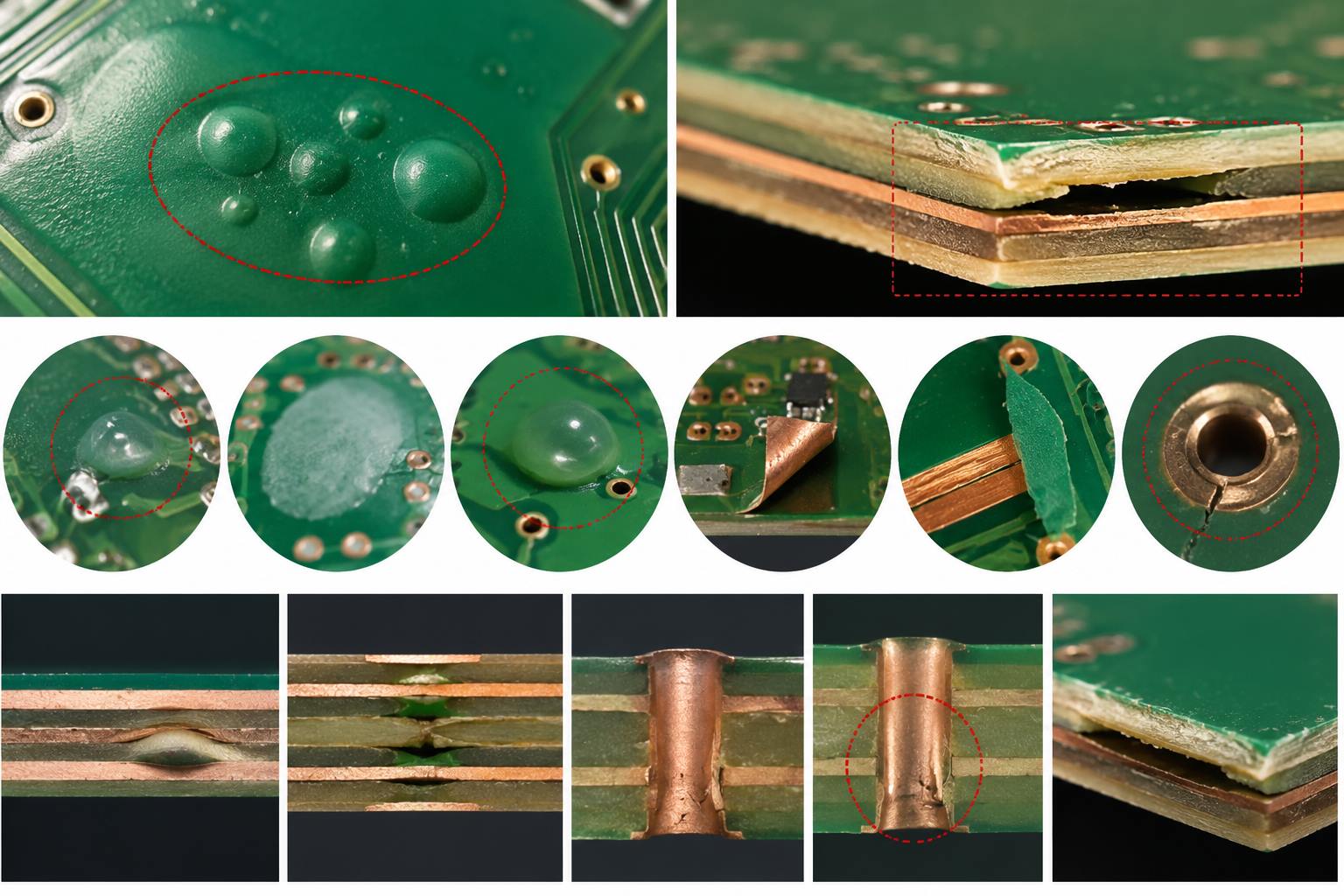
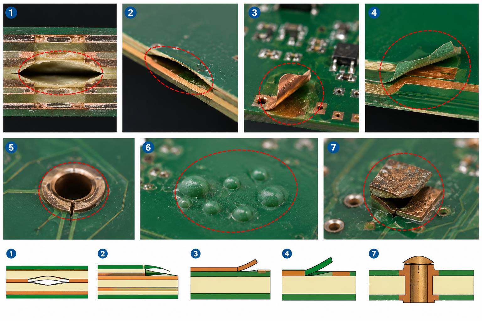
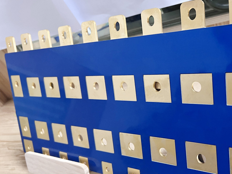
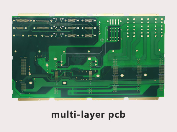
PCB manufacturing PCB manufacturing
Home > Blog

IPC-TM-650: PCB Test Methods for Quality, Reliability, and Process Control

May 11th, 2026

IPC-TM-650 helps engineers understand how PCB materials, finishes, solder mask, and assembly surfaces behave under controlled tests. If you buy bare boards or assembled PCBAs, this standard gives you a common technical language.

However, many buyers only see method numbers on drawings or reports. This guide explains the practical meaning behind those tests. It also shows how EBest Circuit uses engineering review, process control, and testing support to reduce sourcing risk.

ipc-tm-650

What Is IPC-TM-650?

IPC-TM-650 is a test methods manual for printed boards and related electronics materials. It gives defined ways to test chemical, mechanical, electrical, and environmental performance.

In simple terms, IPC-TM-650 helps engineers avoid vague quality claims. Instead, you can ask for a known test method, a clear condition, and a measurable result.

What It Means

For example, a PCB supplier may say a solder mask has strong adhesion. That sounds useful, yet it needs proof. With the right method, you can compare results across batches, suppliers, and design revisions.

Also, IPC-TM-650 does not replace your full product standard. It supports your quality plan. So, engineers often use it together with IPC-A-600, IPC-6012, IPC-A-610, or customer drawings.

AreaWhat It Helps CheckTypical Engineering Concern
ElectricalInsulation and leakageLong-term signal stability
MechanicalPeel, adhesion, flatnessAssembly fit and durability
ChemicalCleanliness and residuesCorrosion and field failures
EnvironmentalHeat, humidity, and stressReliability in real use

Why Is IPC-TM-650 Important for PCB Manufacturing?

IPC-TM-650 matters because PCB quality cannot rely on appearance alone. A board can look clean and still carry ionic residue. Also, a board can pass visual inspection and still warp during assembly.

Because of this, engineers need practical test methods. These methods help control PCB reliability, material testing, process control, and quality assurance.

Quality Needs Evidence

First, the standard supports supplier communication. Your drawing can state a test method, limit, sample size, and acceptance rule. As a result, both teams work from the same baseline.

Next, it supports repeatable process control. If a process changes, the factory can compare old and new test data. This makes engineering review faster and more factual.

Engineer’s tip: Use IPC-TM-650 when a PCB feature affects reliability, assembly yield, or field service life.

Finally, these tests help during supplier qualification. For instance, medical, automotive, aerospace, and industrial projects often need stronger traceability. In those cases, IPC-TM-650 can support a deeper quality file.

IPC-TM-650 Testing Methods for Solder Mask

IPC-TM-650 testing methods for solder mask help check how the mask protects copper and supports assembly. The solder mask must resist heat, chemicals, cleaning, and handling.

However, solder mask quality is not only about color or gloss. It also relates to adhesion, thickness, cure level, hardness, and ionic cleanliness.

Why Solder Mask Matters

Solder mask separates conductive features and helps reduce solder bridging. Also, it protects copper from oxidation during storage and use. This matters more on dense boards with small spacing.

For example, a fine-pitch medical sensor board may need stable mask registration. In contrast, a high-power LED board may need better thermal and surface durability.

Solder Mask CheckWhat It Looks ForWhy Engineers Care
AdhesionMask bond strengthLess peeling after assembly
Cure qualityProper hardeningBetter chemical resistance
RegistrationOpening alignmentStable pad exposure
CleanlinessResidue levelLower leakage risk

Therefore, solder mask testing is useful for boards with dense routing, fine-pitch parts, or harsh operating environments. It gives engineers more confidence before PCBA assembly starts.

How Does IPC-TM-650 Measure Bow and Twist?

IPC TM 650 bow and twist testing helps measure PCB flatness. This matters because warped boards can create placement, soldering, and final assembly problems.

In many cases, engineers refer to ipc tm 650 method 2.4 22 bow & twist. This method gives a structured way to check deviation from a flat plane.

Bow Versus Twist

Bow means the board curves along one direction. Twist means one corner rises while other areas remain lower. Both can affect SMT assembly.

For instance, a warped panel may not sit flat in the printer. Then solder paste height can vary. After that, components may shift or tombstone during reflow.

Also, bow and twist can become worse after thermal stress. High copper imbalance, uneven stack-up, and poor panel design can all add risk.

Flatness IssueCommon CauseAssembly Impact
BowLaminate stressPoor stencil contact
TwistUneven copper balancePlacement offset
Panel warpBad panel supportReflow variation
Thermal warpStack-up mismatchSolder joint stress

As a rule, review flatness early when your board is thin, large, or copper-heavy. This can prevent late-stage assembly delays.

How Is Surface Insulation Resistance Tested Under IPC-TM-650?

Surface insulation resistance testing under IPC-TM-650 checks how well a surface resists current leakage. Engineers often use it for reliability studies and contamination checks.

The keyword ipc-tm-650 2.6.3.7 surface insulation resistance often appears in technical searches. It relates to SIR testing under controlled conditions.

What SIR Shows

IPC TM 650 insulation resistance tests help reveal weak surface insulation. Moisture, flux residue, and ionic contamination can reduce the measured resistance.

Because of this, SIR matters in medical devices, industrial controls, sensors, and communication boards. These products often work in warm or humid settings.

For example, a board may pass electrical testing at room temperature. However, it may show leakage after humidity exposure. SIR testing helps find that risk earlier.

SIR FactorPossible SourceEngineering Risk
Flux residueIncomplete cleaningLeakage current
MoistureStorage or use environmentLower insulation resistance
Ionic saltsProcess chemicalsCorrosion path
Fine spacingDense PCB layoutHigher leakage sensitivity

In short, SIR testing gives more than a pass or fail result. It helps you understand process cleanliness and long-term board behavior.

IPC-TM-650 Cleanliness and Ionic Contamination Testing

IPC TM 650 cleanliness tests help control residues from fabrication and assembly. These residues can come from flux, plating chemistry, cleaning agents, or handling.

IPC TM 650 ionic contamination testing is especially important for high-reliability PCBA. It helps measure mobile ionic material that may affect electrical performance.

Residues Create Risk

Cleanliness is easy to underestimate. A board can look clean under normal light and still carry harmful residues. Therefore, visual inspection alone is not enough.

In particular, ionic residues can absorb moisture. Then they may form leakage paths between conductors. Over time, this can lead to corrosion or dendritic growth.

IPC TM 650 ionic contamination limits depend on the test method, product use, and customer requirement. So, engineers should define limits before production starts.

How EBest Circuit handles this: We review materials, flux type, cleaning process, and testing needs before PCBA production begins.

Cleanliness TopicWhat To DefineBest Time To Review
Flux chemistryNo-clean or washableBefore SMT setup
Cleaning processAgent and cycleBefore trial run
Ionic limitCustomer requirementBefore quotation
Sampling planLot and frequencyBefore mass build

Overall, cleanliness control works best when design, process, and inspection teams align early. This is more efficient than fixing failures later.

Common IPC-TM-650 Mechanical and Adhesion Tests

IPC-TM-650 mechanical tests help check whether the PCB can survive fabrication, assembly, and field handling. These tests can include peel strength, tape testing, and adhesion testing.

Engineers often search for ipc tm 650 tape test, ipc tm 650 adhesion test, and ipc tm 650 peel strength. These topics matter when copper, solder mask, or surface layers must stay stable.

Adhesion Affects Reliability

Adhesion is important because PCB layers work as a system. Copper must bond well to the laminate. Also, solder mask must stay attached through heat and cleaning.

For example, poor peel strength can affect heavy copper boards. It can also affect edge plating, press-fit zones, and high-current terminals.

On the other hand, a simple consumer board may not need the same test depth. The right test plan should match product risk, not just a checklist.

Test AreaUseful ForCommon Product Type
Peel strengthCopper bond checkPower and heavy copper PCB
Tape testSurface adhesion checkSolder mask and marking
Adhesion testLayer stability checkIndustrial and automotive PCB
Thermal stressHeat resistance checkReflowed PCBA

Most importantly, these tests should support the design goal. A strong test plan starts with your application, not with a random standard list.

IPC-TM-650 Solderability Test and Copper Foil Testing

IPC TM 650 solderability test methods help check whether PCB pads can accept solder properly. This matters during SMT, wave soldering, selective soldering, and manual rework.

Also, ipc-tm-650 thermal conductivity copper foil searches often relate to material behavior. Engineers may need copper data for power, thermal, or high-current designs.

Solderability Drives Yield

Solderability affects first-pass yield. If pads oxidize or the finish performs poorly, solder joints may look dull or incomplete. Then rework cost can rise.

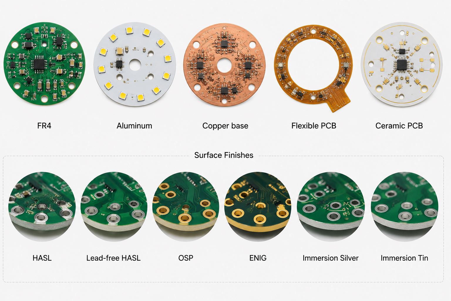
For instance, ENIG, OSP, immersion silver, and HASL each need proper storage and process control. Therefore, surface finish choice should match your assembly path.

CheckWhat It SupportsTypical Concern
SolderabilityPad wettingPoor joint formation
Copper foilMaterial stabilityThermal or current load
Surface finishAssembly shelf lifeOxidation or handling
Thermal exposureReflow performanceDelamination or stress

In general, solderability review should happen before production. This is especially true when components have fine pitch, bottom termination, or high thermal mass.

IPC-TM-650 for Prototype and Low-Volume PCB Builds

IPC-TM-650 is not only useful for large production. It can also help prototype and low-volume PCB builds move faster with fewer surprises.

Prototype teams often change materials, stack-ups, finishes, or components. Because of this, they need fast engineering feedback before committing to a larger build.

Better Prototype Decisions

First, test data helps you compare design options. For example, you can review flatness risk on a thin board before assembly. Then you can adjust the stack-up or panel plan.

Next, cleanliness and SIR checks can support early reliability review. This is useful for medical, sensing, RF, and industrial products. These products often need stable field behavior.

Also, solderability review helps when your BOM includes fine-pitch ICs or hard-to-source parts. A small issue in surface finish can waste expensive components.

Prototype NeedHelpful IPC-TM-650 AreaPractical Outcome
Thin PCBBow and twistBetter SMT stability
Fine-pitch layoutCleanliness and SIRLower leakage risk
High-power boardCopper and adhesionStronger thermal design
New surface finishSolderabilityHigher assembly yield

As a result, prototype testing can reduce redesign time. It also helps your team decide what to control during the next production stage.

How EBest Circuit Supports IPC-TM-650 Based PCB Quality Control?

EBest Circuit supports IPC-TM-650 based quality control through engineering review, controlled fabrication, PCBA process planning, and traceable production data. We connect these steps before your order enters production.

However, we do not treat testing as a separate final step. Instead, we use test needs to guide DFM, material choice, process flow, and inspection planning.

1 Account Manager + 3 Engineers

Each project receives one account manager and three engineers. The team covers DFM review, process planning, and quality control. As a result, communication stays clear from RFQ to shipment.

DFM and BOM Review

We include a DFM pre-review report and BOM optimization list with every order. This helps you find layout, material, component, and process risks early.

Certified Manufacturing System

EBest Circuit works under ISO 9001, ISO 13485, IATF 16949, and AS9100D systems. Therefore, we can support medical, automotive, aerospace, and industrial electronics projects.

Own Factories and Supply Chain

We operate our own PCB factory and own PCBA factory. In addition, we work with more than 1,000 supply chain partners. This helps us control lead time, materials, and assembly flow.

Prototype to Volume Support

We support prototypes, small batches, and volume production. For PCBA prototypes, our typical turnaround is about 1.5 weeks from build to shipped tested boards.

Digital MES Traceability

Our digital MES supports fast material and batch traceability. In many cases, teams can trace key production data within 5 seconds. This helps regulated projects manage records better.

20 Years of PCBA Experience

EBest Circuit has 20 years of PCBA experience. We have served more than 10,000 engineers and 1,800 customers. Because of this, we understand both engineering detail and delivery pressure.

To get a quote, send your Gerber files and BOM to sales@bestpcbs.com. We respond with a DFM report and quote within 24 hours.

FAQs About IPC-TM-650 Test Methods

What is IPC-TM-650 used for in PCB manufacturing?

IPC-TM-650 is used to define test methods for PCB materials, solder mask, cleanliness, insulation resistance, bow and twist, adhesion, solderability, and other quality checks.

Is IPC-TM-650 required for every PCB order?

IPC-TM-650 is not needed for every basic PCB order. However, it is useful when your product needs stronger proof of reliability, process control, or material performance.

Which IPC-TM-650 test checks bow and twist?

Bow and twist are commonly linked with IPC-TM-650 method 2.4.22. This method helps check PCB flatness after fabrication or thermal stress.

How does ionic contamination affect PCBA reliability?

Ionic contamination can attract moisture and create leakage paths. As a result, it may reduce insulation resistance and affect long-term PCBA reliability.

Can EBest Circuit support prototypes with IPC-TM-650 based controls?

Yes. EBest Circuit supports prototypes, small batches, and volume builds with DFM review, process planning, PCBA testing, and traceability control.

How do I request IPC-TM-650 test support from EBest Circuit?

You can send your Gerber files, stack-up, drawings, and BOM to sales@bestpcbs.com. We will review the project and suggest suitable quality control steps.

You may also like

What is a QR code PCB? PCB QR code size

May 8th, 2026

What exactly is a QR code PCB?

A QR code PCB is a printed circuit board that carries a readable QR code directly on its surface. The code can be placed on the silkscreen layer, solder mask opening area, copper-free marking zone, label area, or laser-marked region, depending on the product’s traceability needs and manufacturing method. In practical production, this small square code can connect a circuit board to its batch data, production records, test results, BOM version, inspection history, firmware version, warranty information, or customer-specific tracking system.

For electronics manufacturers, a QR code on PCB is much more than a visual mark. It acts like a digital identity for the board. When a technician scans it, the system can retrieve useful information within seconds. This is very helpful for PCBA assembly, incoming inspection, quality control, repair, field service, and after-sales analysis.

A PCB QR code can store direct text, a serial number, a URL, a production lot number, or a database reference. In most professional manufacturing systems, the code itself does not need to carry all information. It may only contain a unique ID, while the full data is stored in a factory MES, ERP, quality database, or customer traceability platform. This approach keeps the code compact and easier to scan.

In the PCB industry, QR marking is widely used for industrial electronics, medical electronics, automotive control boards, communication modules, power control boards, smart devices, and OEM assemblies. At EBest Circuit (Best Technology), QR code marking is often treated as part of a broader traceability strategy rather than a simple printing request. The value comes from connecting the physical board to reliable production data, inspection records, and engineering control points.

How is a QR code printed onto a PCB?

A QR code can be applied to a PCB in several ways. The most common methods are silkscreen printing, laser marking, inkjet printing, and label-based marking. Each method has its own strengths. The best option depends on the board material, surface finish, code size, production volume, cost target, operating environment, and scanning distance.

Silkscreen is a familiar choice because most PCBs already include a legend layer. The QR code on PCB can be printed with white, black, or yellow legend ink, depending on the solder mask color and contrast requirement. For standard FR4 boards with enough available surface area, silkscreen can provide a practical and cost-effective solution. It is suitable for product identification, revision marking, internal batch tracking, and general factory scanning.

Laser QR code on PCB is often selected when higher precision, better durability, or smaller marking size is needed. A laser can mark the solder mask, exposed copper, metal surface, ceramic substrate, or certain special materials with excellent edge definition. It is a strong option for compact boards, high-density assemblies, harsh environments, and products that require long-term identification.

Inkjet printing is also used in some production lines, especially when variable data is needed at higher speed. A PCB QR code printer can generate unique codes for each board or panel. This method can work well when linked with automated handling equipment and traceability software. Adhesive labels are another option, but they are usually used when direct marking is impractical or when additional human-readable information must be included.

Before printing or marking, the code data must be generated, verified, and placed in the PCB design or production file. For custom QR code PCB orders, the manufacturer may ask for the encoded content, preferred size, position, marking color, serial number format, and scanning requirements. For volume production, the code may be dynamically generated during manufacturing.

MethodBrief DescriptionBest Use CaseMain Advantage
Silkscreen printingQR code printed with legend inkStandard PCB identification and batch trackingCost-effective and easy to integrate
Laser markingCode engraved or marked with laser energyCompact boards, durable marking, industrial useHigh precision and strong permanence
Inkjet printingVariable code printed during productionAutomated serialization and high-volume trackingFlexible for changing data
Adhesive labelPrinted label attached to PCB or productBox build, prototypes, or limited board spaceCan include larger text and barcode data

For stable results, EBest Circuit (Best Technology) usually recommends confirming the marking method during DFM review. This helps avoid placement conflicts with pads, test points, tooling holes, conformal coating zones, and assembly fixtures.

What are the main uses of QR code PCB?

The main use of a QR code PCB is traceability. A well-designed code allows engineers, operators, and quality teams to identify a board quickly and connect it with the right production information. In a modern electronics factory, this supports faster decision-making and cleaner documentation.

A QR code on circuit board can be used during bare board manufacturing, PCBA assembly, final testing, shipment, repair, and field service. During PCB fabrication, the code may identify the panel number, material batch, surface finish, manufacturing date, and inspection result. During assembly, it may connect to solder paste inspection data, SMT line information, reflow profile, AOI results, X-ray inspection, ICT records, functional test data, and packaging status.

Common uses include:

  • Batch tracking for bare PCBs and assembled boards
  • Serial number control for each finished unit
  • Revision identification for engineering changes
  • Production history lookup during quality review
  • Test data connection for ICT, FCT, AOI, or burn-in
  • Warranty and repair record access
  • Anti-mixing control in high-mix assembly lines
  • Customer-specific product authentication

Another useful application is internal process control. When a board moves from SMT assembly to DIP assembly, coating, testing, packing, or box build, scanning the code can confirm its route and status. This reduces manual recording work and improves accountability across each stage. For projects with many similar board versions, QR scanning brings welcome clarity.

At EBest Circuit (Best Technology), this type of marking can be integrated with turnkey PCB and PCBA production. For customers who need stronger visibility, the QR code can become part of a larger tracking workflow that includes material sourcing, fabrication, assembly, testing, and shipment documentation.

Can QR code silkscreen PCB support batch tracking?

Yes, a QR code silkscreen PCB can support batch tracking when the code is designed, printed, and managed correctly. In many standard projects, silkscreen marking is enough for batch-level traceability. The code can represent a production lot, order number, customer part number, panel number, or revision code. When scanned, it can connect operators to the related manufacturing record.

For batch tracking, the most important point is data structure. The QR code should follow a clear naming and numbering rule. A simple random code may be readable, but it becomes much more useful when it follows a controlled system. For example, a code may include the customer code, product number, PCB revision, batch date, and production sequence. In automated systems, the code may only store a unique ID, while the database stores the full record.

For batch-level tracking, the same code may appear on every PCB within the same batch. For unit-level serialization, each board needs a different code. Silkscreen can support variable data in some production setups, but laser or inkjet marking is usually more efficient for unique serial numbers. That is why the marking method should match the tracking depth.

Tracking TypeDescriptionSuitable Marking MethodTypical Application
Batch trackingOne code represents one production lotSilkscreen, laser, inkjetBare PCB lot control, incoming inspection
Panel trackingOne code identifies a manufacturing panelSilkscreen or laserFabrication and assembly workflow
Unit serializationEach board has a unique codeLaser or inkjet preferredMedical, industrial, automotive, high-value electronics
Process trackingCode updates or links to route statusLaser, inkjet, database-linked codeSMT, testing, repair, final QA

EBest Circuit (Best Technology) can support different traceability levels based on the customer’s product risk, industry requirements, and production volume. For simple projects, batch tracking is often enough. For high-reliability projects, unit-level control gives stronger confidence and better field analysis.

Does QR code marking on PCB affect circuit performance?

QR code marking on PCB is designed to avoid circuit performance issues when it follows correct layout and manufacturing rules. In most cases, the code is placed in a non-electrical area such as the silkscreen layer, solder mask area, board edge, panel rail, or dedicated marking zone. Since the code does not function as part of the circuit, it should be separated from sensitive copper features, pads, impedance-controlled traces, RF sections, high-voltage spacing, and thermal contact surfaces.

For RF, high-speed, high-voltage, or power boards, placement becomes more critical. A QR code should stay away from antenna areas, controlled impedance lines, creepage paths, heat sink contact zones, and exposed copper regions. If laser marking removes or changes solder mask in a sensitive area, the design team should review the effect before release. Good practice is simple: reserve a clean marking area early in layout rather than placing the code at the last moment.

EBest Circuit (Best Technology) usually handles this through engineering review. The QR code location can be checked together with DFM items such as component clearance, fiducial placement, panelization, tooling holes, solder mask clearance, and test point access. This helps keep the board readable, manufacturable, and electrically reliable.

Is custom QR code PCB available for private design?

Yes, custom QR code PCB is available for private design, OEM projects, and customer-specific traceability systems. A manufacturer can place a code according to the customer’s preferred location, size, content, marking method, and brand requirement. The code may be visible on the finished product, hidden inside an enclosure, placed on a panel rail for production use, or located on the assembled board for field service.

Custom marking is especially useful when a company wants to protect its design data, organize product versions, or connect boards with internal management systems. For private design projects, the QR code can link to secure records rather than public web pages. This means only authorized staff can access the detailed information after scanning. The visible code may look simple, while the database behind it contains a rich production history.

Typical custom content may include:

  • Customer part number
  • PCB revision
  • Production date
  • Lot number or serial number
  • Assembly version
  • Internal item code
  • Test record ID
  • Warranty or service reference
  • Secure URL or database lookup code

Custom QR code PCB orders should be discussed before fabrication files are finalized. The customer can define whether the code should appear in Gerber data, be generated during production, or be added by the manufacturer according to a serialization rule. If the code needs to change per board, the manufacturer needs a controlled data file or a system connection. If the same code applies to all boards, it can be integrated into the normal silkscreen artwork.

EBest Circuit (Best Technology) can support customer-specific marking needs across prototype, small batch, and volume production. For OEM customers, this can be combined with PCB fabrication, component sourcing, PCBA assembly, testing, and final packaging to create a smoother production handoff.

What’s the advantage of PCB with QR code?

The main advantage of a PCB with QR code is fast, reliable access to board-level information. Instead of relying only on paper labels, manual notes, or file names, the physical board carries a digital reference that follows it through production and use.

In electronics manufacturing, small errors can create large delays. A wrong revision, mixed batch, missing test record, or unclear repair history can slow down delivery and increase review time. A scannable code gives operators a direct way to confirm the board identity. When connected to a database, it can show the build status, production route, inspection result, or customer order details.

For quality control, QR marking helps create a stronger evidence chain. If a customer reports a field issue, the manufacturer can trace the affected board back to its production batch, material lot, inspection data, and test result. This supports faster root cause analysis and more confident corrective action. For products used in medical, industrial, automotive, aerospace, or communication equipment, this visibility is a clear operational advantage.

AdvantageWhat It Means in PracticeValue for Customer
Faster identificationScan the board instead of manually reading long codesSaves inspection and service time
Better traceabilityConnects the board to production and test recordsImproves quality control
Cleaner version controlConfirms revision and product model quicklyReduces mix-up risk
Efficient repair supportLinks to previous repair or test historySpeeds up troubleshooting
Stronger documentationSupports batch records and audit reviewHelpful for regulated industries
Scalable production controlWorks with MES, ERP, and warehouse systemsSupports growth and repeat orders

A QR code on circuit board also helps communication between supplier and customer. When both sides use the same code reference, discussions become clearer. Instead of describing a board by photo, file name, or partial marking, both teams can refer to the same scan data. This is simple but very powerful during engineering changes and after-sales support.

EBest Circuit (Best Technology) sees QR marking as a practical way to strengthen manufacturing discipline. It does not replace good process control, but it makes that control easier to verify. For customers who value dependable production and transparent communication, this small mark can create a big improvement in workflow confidence.

How durable is QR code printing on circuit boards?

The durability of QR code printing on circuit boards depends on the marking method, board surface, operating environment, cleaning process, coating treatment, and handling conditions. A properly designed and manufactured code can remain readable through assembly, testing, shipment, and long-term use. For products that face heat, moisture, solvents, abrasion, or outdoor exposure, the marking method should be selected with extra care.

Silkscreen QR codes are durable enough for many standard electronics. The legend ink is cured onto the solder mask and can withstand normal assembly processes. It works well for indoor electronics, control boards, consumer devices, power supplies, and many industrial products. However, repeated abrasion, aggressive cleaning agents, or heavy conformal coating can reduce readability. Good placement helps protect the code from wear.

Laser marking is often more durable because it changes the surface rather than sitting only as an ink layer. A laser QR code on PCB can resist cleaning, handling, and long service life more effectively. It is often preferred for compact industrial boards, automotive modules, medical electronics, metal substrates, ceramic PCBs, and products that need permanent identification. The exact durability depends on the substrate and laser process settings.

Inkjet marking can be effective when the right ink and curing method are used. It is useful for fast serialization, especially in automated production. The ink must be compatible with solder mask, cleaning chemistry, and operating temperature. Adhesive labels can provide good readability, but their long-term performance depends on adhesive quality, temperature range, humidity, and available bonding surface.

Marking MethodDurability LevelSuitable EnvironmentNotes
SilkscreenGood for standard useIndoor electronics, general assembliesBest with good contrast and protected location
Laser markingVery strong for permanent IDIndustrial, medical, automotive, harsh-use productsExcellent for small and precise codes
Inkjet printingGood with correct inkAutomated serialized productionNeeds process validation
Label markingVaries by label materialBox build, enclosure, large ID areaAdhesive quality is important

For harsh environments, it is wise to test scanning after cleaning, reflow, coating, thermal cycling, or aging. EBest Circuit (Best Technology) can review the product environment and suggest a suitable approach. This helps the code remain readable when the board reaches real use, not only when it leaves the production line.

Can QR code PCB be used in industrial electronics?

Yes, QR code PCB can be used very effectively in industrial electronics. In fact, industrial products are one of the strongest use cases for board-level identification. Industrial control boards, power modules, automation equipment, sensors, motor drives, communication gateways, test instruments, and monitoring systems often require long service life, stable documentation, and fast maintenance support. A scannable board identity makes these tasks easier.

Industrial electronics are frequently produced in multiple revisions over several years. A control board may look almost the same from the outside while its firmware, component alternatives, connector choices, or circuit revision changes over time. A QR code on PCB helps maintenance teams identify the exact board version before replacement or repair. This is very useful when equipment downtime is costly.

For factories and equipment makers, QR codes also support spare part management. A technician can scan the board and confirm whether the replacement part matches the machine model. The code may connect to installation instructions, calibration records, test data, or service logs. In large facilities, this improves maintenance speed and reduces the chance of using the wrong board.

In industrial electronics, the QR code should be part of the product design plan, not a late decoration. Designers should reserve enough space, define scanner access, check coating coverage, and confirm the code remains visible after assembly. When the board is installed vertically or inside a narrow housing, scanning angle becomes important. A readable code in CAD may be hard to scan in the finished machine if access is limited.

EBest Circuit (Best Technology) supports industrial customers with PCB fabrication, PCBA assembly, testing, and traceability-oriented manufacturing. For control systems, automation equipment, and durable electronics, QR marking can be combined with inspection records and production data to create a more dependable manufacturing record.

What design rules apply to QR code PCB layout?

QR code PCB layout should focus on readability, contrast, size, location, clearance, and manufacturing tolerance. A code that looks fine on screen may become difficult to scan after printing if the modules are too small or the surrounding area is crowded. The goal is simple: make the code easy for scanners, operators, and service teams to read under real production conditions.

PCB QR code size is one of the most important design points. The minimum size depends on the amount of encoded data, QR version, error correction level, marking method, scanner quality, and required scanning distance. For many PCB silkscreen applications, a practical size may start around 5 mm × 5 mm for very simple data, but 7 mm × 7 mm to 10 mm × 10 mm is often more comfortable for reliable factory scanning. For laser marking, smaller codes may be possible because the edge definition is sharper. For manual handheld scanning, larger is usually better.

The code should also include a quiet zone. This is the blank margin around the QR pattern. Without enough margin, nearby text, copper, pads, components, or solder mask openings may disturb recognition. A quiet zone of at least four modules is a common QR code principle. On PCB artwork, this means the designer should keep the area around the code clean.

Useful layout rules include:

  • Reserve a clean rectangular marking area early in PCB layout.
  • Keep the code away from component pads, vias, test points, fiducials, and screw holes.
  • Maintain a quiet zone around the QR pattern.
  • Avoid placing the code under tall components, shields, heat sinks, or labels.
  • Select a size that matches the marking method and scanner distance.
  • Use short encoded data when space is limited.
  • Confirm readability after soldering, washing, coating, and final assembly.
  • Keep codes away from RF antenna zones, high-voltage spacing areas, and thermal contact surfaces.

For PCB QR code size planning, the amount of data matters. A short serial number can use fewer modules and stay readable at a smaller size. A long URL or dense information needs more modules, which requires a larger printed area. In many professional systems, using a short unique ID is better than encoding a long data string. The ID can point to a database where full records are stored.

Design FactorPractical RecommendationWhy It Matters
Code sizeUse a comfortable size, often 7–10 mm or larger for silkscreenImproves scanning reliability
Data lengthKeep encoded content short when possibleReduces module density
Quiet zoneLeave clean space around the codeHelps scanner detect the pattern
LocationPlace in a visible, protected areaSupports scanning after assembly
ContrastUse strong color differenceImproves recognition speed
SurfaceAvoid uneven, reflective, or crowded areasKeeps edges readable
ProcessMatch design to silkscreen, laser, or inkjet capabilityPrevents production mismatch

For a well-built result, the QR code should be reviewed together with the full PCB stack, surface finish, solder mask color, assembly layout, and end-use environment. This is where cooperation with an experienced manufacturer becomes valuable. EBest Circuit (Best Technology) can help customers check QR code placement, marking method, manufacturability, and traceability needs before production begins.

In summary, a PCB with a scannable QR code gives engineers and manufacturers a practical way to connect a physical circuit board with useful digital information. For custom PCB and PCBA projects that need professional QR marking support, contact sales@bestpcbs.com

You may also like

Custom PCB Power Supply: Layout Guide & Wholesale Assembly Tips

May 7th, 2026

A custom PCB power supply is a printed circuit board designed and manufactured to deliver precise electrical power — specific voltage levels, current capacity, and protection features — tailored to the exact requirements of a product rather than relying on a generic off-the-shelf module. For engineers working on medical devices, industrial controllers, automotive systems, or consumer electronics, getting the power supply right at the PCB level is fundamental to product reliability, thermal performance, and long-term field stability.

This guide covers everything engineers need to know about custom PCB power supply design and wholesale assembly: material selection, layer stack-up, copper thickness, surface finish options, DFM best practices, and how to choose a manufacturing partner who can support you from first prototype through high-volume production.

At EBest Circuit (Best Technology), we have spent 20 years working directly with engineers on exactly this type of project. Every order is handled by a dedicated team of one business partner and three specialized engineers — covering R&D, PCB process, and PCBA assembly — so your technical questions get engineering answers, not sales responses. We hold ISO 9001, ISO 13485, IATF 16949, and AS9100D certifications, run our own PCB and PCBA factory, and consistently deliver full PCBA within 1.5 weeks. If you have a project in mind, feel free to reach out to our team at sales@bestpcbs.com — we are happy to review your requirements and provide a practical assessment.

Custom PCB Power Supply

Why Engineers Choose Custom PCB Power Supply Boards?

Off-the-shelf power supply modules are a convenient starting point, but they rarely satisfy the exacting demands of modern electronics. Whether you are developing a medical device, an industrial controller, automotive electronics, or next-generation consumer hardware, a custom PCB power supply allows you to optimize every parameter — voltage rails, switching frequency, thermal dissipation, EMI shielding, footprint, and reliability — to match your exact application.

Engineers worldwide increasingly choose custom designs for these concrete reasons:

  • Precise Power Rails: Define multiple voltage outputs, tight tolerances, and load-step response exactly as your BOM demands — no compromises from a generic module.
  • Thermal Optimization: Position power components, copper pours, and thermal vias exactly where thermal simulation says they need to be. Metal-core (aluminum/copper) substrates are available for high-power density designs.
  • Form-Factor Freedom: From 3×3 mm microboards to 580×890 mm production panels, custom PCBs fit your mechanical envelope — not the other way around.
  • IP Protection: Your custom design stays proprietary. No competitor can buy the same module and replicate your product performance.
  • Cost-Efficient Scaling: A custom BOM-optimized design reduces unit cost significantly at volume. Wholesale PCBA is where the real savings are realized.
  • Compliance-Ready Design: Design for UL, CE, IEC 62368, or IATF16949 from day one, with an experienced engineering partner who understands certification requirements.

Power Supply PCB Design Essentials

A high-performance custom power supply PCB is the result of dozens of carefully balanced decisions. Below are the most critical areas where design choices directly affect reliability, efficiency, and manufacturability.

1. Topology Selection

The power conversion topology shapes every subsequent design decision. For isolated designs — such as medical or industrial applications — flyback, LLC resonant, or phase-shifted full-bridge are popular choices. For non-isolated point-of-load (POL) regulators, synchronous buck or multi-phase buck are industry standards. Your selection affects transformer design, control IC selection, switching node layout, and EMC strategy.

2. Layer Stack-Up and Current Carrying Capacity

Power supply PCBs carrying more than 5 A require careful stack-up planning. Wide power planes, thick copper, and strategic via stitching keep IR drop and thermal rise within spec. For high-current designs, our manufacturing supports outer copper up to 10 oz (standard) and up to 28 oz (advanced prototype) — one of the highest capabilities available from a China-based manufacturer.

3. EMI Control Layout

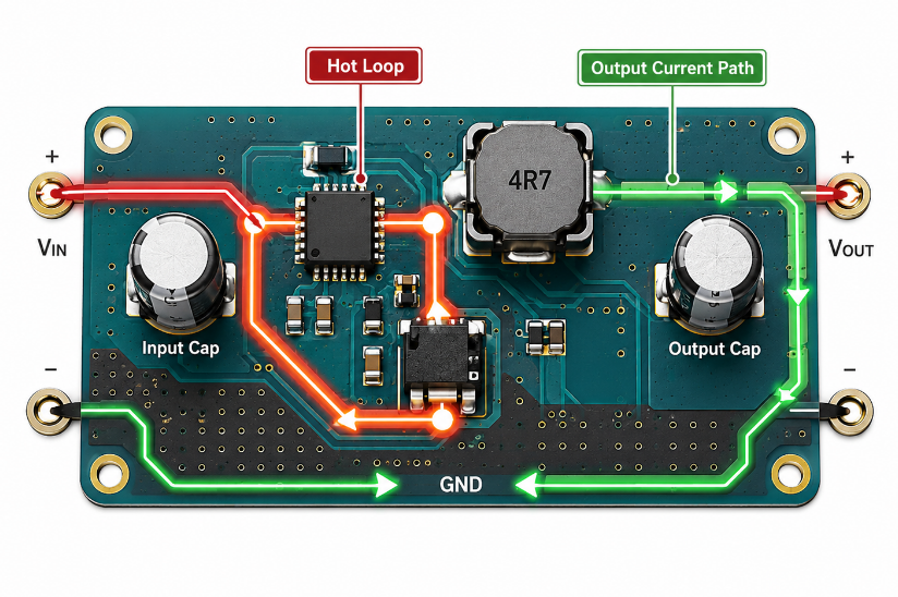
Switching power supplies are inherently noisy. The PCB layout must minimize high-di/dt loop areas, place input capacitors as close as possible to the switch nodes, separate analog and power ground planes, and route gate-drive traces with care. A key rule of thumb: the highest-frequency current loop (e.g., MOSFET drain–capacitor–MOSFET source) must be minimized in physical area. For every doubling of loop area, radiated EMI increases approximately 6 dB — enough to fail FCC/CE limits.

4. Impedance Control and Signal Integrity

If your power supply includes digital control (digital PWM, PMBus, I²C), controlled impedance traces are critical. Our standard capability holds impedance to ±5 Ω for values below 50 Ω, and ±10% for 50 Ω and above. Advanced prototype tolerance reaches ±4 Ω / ±6%.

5. Thermal Via Strategy

Thermal vias under power pads (QFN, DFN, TO-263) are essential for junction-temperature management. Proper via fill, pitch, and diameter selection prevents solder voiding while maximizing thermal conductance. Our engineering team provides via-fill recommendations as part of every DFM report.

Material and Layer Selection for Power Supply PCBs

Material selection is the single most impactful decision for long-term power supply reliability. Different applications demand different substrates.

Material TypeTg / Key PropertyBest ApplicationAvailable Brands
FR4 Standard Tg130–140 °CConsumer, low-temp industrialKB 6160, Shengyi S1141
FR4 Mid Tg150 °CIndustrial, higher ambientKB 6165, Isola IT158, S1000H
FR4 High Tg170–180 °CAutomotive, high-load power supplyIT180A, S1000-2M, FR408, TU-768
High CTICTI ≥ 600 VHigh-voltage isolated PSUS1600L, KB-6165C
High-Speed / Low-LossLow Dk/DfGaN/SiC PSU, switching >1 MHzM4/M6/M7, TU-872SLK, IT-958
Metal Core (Aluminum)0.3–6 W/m·K thermal conductivityLED drivers, high-power PSU1100/5052/6061 alloy, Bergquist
Metal Core (Copper)Up to 12 W/m·K (advanced)Ultra-high-power density designsPure copper substrate

Most power supply designs fall in the 4–8 layer range. Complex digital-power hybrid designs for servers or telecom can reach 16–24 layers with embedded planes for PDN (Power Distribution Network) optimization. Our standard capability covers 1 to 50 layers, with up to 100 layers available on engineering review.

EBest Circuit Manufacturing Capabilities

When you order a customized power supply PCB assembly from EBest Circuit, you benefit from one of the most comprehensive process capability tables available. The data below is drawn directly from our certified process capability documentation.

ParameterStandard CapabilityAdvanced (Prototype)
Layer Count1–50 layersUp to 100 layers (on review)
Board Thickness0.4 mm – 6 mm0.15 mm – 10 mm
Outer Copper Thickness0.5 oz – 10 oz0.5 oz – 28 oz
Inner Copper Thickness0.5 oz – 6 oz0.5 oz – 20 oz (≥12 oz on review)
Laser Drill Min. Diameter0.10 mm0.070 mm
Mechanical Drill Range0.15 mm – 6.5 mm0.15 mm minimum
Min. Board Size10 × 10 mm3 × 3 mm
Max. Board Size (≥3 layers)580 × 762 mm580 × 1220 mm
Min. Line Width / Spacing3/3 mil (outer)2/2 mil (outer)
Impedance Tolerance±5 Ω / ±10%±4 Ω / ±6%
Warp and Twist (Bow)≤ 0.75%≤ 0.50%
Max. Test Voltage5,000 V DC / 3,000 V AC
Metal Core (Al/Cu)1–6 layers, 0.5–5 mm thick>6 layers (on review)
Back-Drill Depth Precision±0.1 mm
Thermal Conductivity (Metal Core)0.3–6 W/m·KUp to 12 W/m·K

DFM Analysis: How We Help Engineers Avoid Costly Mistakes

Design for Manufacturability (DFM) review is not a checkbox — it is the single most valuable service we provide before a single PCB is fabricated. Our team carries 20 years of PCB/PCBA engineering experience and performs a thorough pre-production audit that covers:

  • Gerber vs. BOM cross-check: Verify that every component in your BOM has a corresponding land pattern in the Gerber, with correct polarity markings.
  • Copper clearance and creepage compliance: For high-voltage power supplies, IPC-2221 and IEC 60950/62368 clearance and creepage distances are checked against your isolation requirements.
  • Drill-to-copper and annular ring analysis: Flag any drills that violate minimum annular ring or drill-to-copper spacing for your selected laminate.
  • Solder mask opening audit: Prevent solder bridging and insufficient-solder defects by verifying SM opening ratios against IPC-7527 stencil recommendations.
  • Via-in-pad and thermal relief review: Confirm that thermal vias are properly specified (filled vs. unfilled) and that power pad connections use appropriate thermal relief or solid tie.
  • Component courtyard conflict detection: Identify component-to-component spacing violations that would prevent standard pick-and-place nozzle access.
  • BOM optimization recommendations: Flag obsolete, single-source, or long-lead-time components and suggest qualified alternates from our 1,000+ supply chain partners.
  • Impedance stack-up verification: For controlled-impedance designs, model your stack-up against the target Dk of the selected material and confirm trace widths.

Every project receives a formal written DFM Pre-Screening Report before production is approved. Issues are ranked by severity — Critical, Major, or Advisory — so your team can make informed decisions quickly. This service is included in our engineering support at no additional charge.

Surface Finish Options for Power Supply PCBs

Surface finish choice directly affects solderability, shelf life, contact resistance, and overall long-term reliability. Here is a comparison of the most relevant finishes for power supply applications:

Surface FinishThicknessKey AdvantageBest Application
Lead-Free HASL2–40 µmLow cost, excellent solderabilityStandard industrial PSU, cost-sensitive runs
ENIG (Immersion Gold)Ni: 3–8 µm / Au: 0.025–0.125 µmFlat surface, IC-compatible, long shelf lifeHigh-density SMT, BGA, fine-pitch power modules
Immersion Tin0.8–1.5 µmRoHS, press-fit connector compatibleAutomotive PSU with press-fit connectors
Immersion Silver0.2–0.4 µmExcellent flatness, wire-bondableHigh-frequency/RF supply hybrids
OSP0.1–0.3 µmUltra-flat, lowest cost, RoHSReflow-only assemblies with short storage window
ENEPIGNi: 3–8 µm / Pd: 0.05–0.125 µm / Au: 0.025–0.125 µmWire-bond + solder compatible, no black pad riskHybrid power modules with wire bonding
Hard Gold (Edge Finger)0.1–1.27 µmWear-resistant, low contact resistanceCard-edge connectors, test points

One-Stop PCBA Assembly: From Bare Board to Tested Unit

Our core value proposition is the full integration of PCB fabrication, component procurement, SMT/through-hole assembly, and functional testing under one roof. This eliminates the coordination overhead, quality grey-zones, and lead-time waste that come from splitting your supply chain across multiple vendors.

Step 1 — Engineering Review and DFM Report Your Gerber, BOM, and assembly drawings are reviewed by our engineering team. A written DFM report is issued within 24–48 hours for standard complexity designs.

Step 2 — Component Procurement We source 100% of your BOM through our 1,000+ verified supply chain partners. All components are checked for authenticity and traceability. Counterfeit screening is included for ICs and passives on aerospace and medical builds.

Step 3 — PCB Fabrication Our own factory produces the bare boards to your exact specification. No broker — direct factory control from inner-layer imaging through final electrical test.

Step 4 — SMT and Through-Hole Assembly Automated SMT with AOI (Automated Optical Inspection) after paste printing and after reflow. Manual through-hole and selective soldering for connectors and large power components.

Step 5 — Inspection: X-Ray, AOI, and Visual BGA and QFN solder joints are verified by X-ray inspection. 3D AOI is applied on all boards. IPC-A-610 workmanship standard is applied by default.

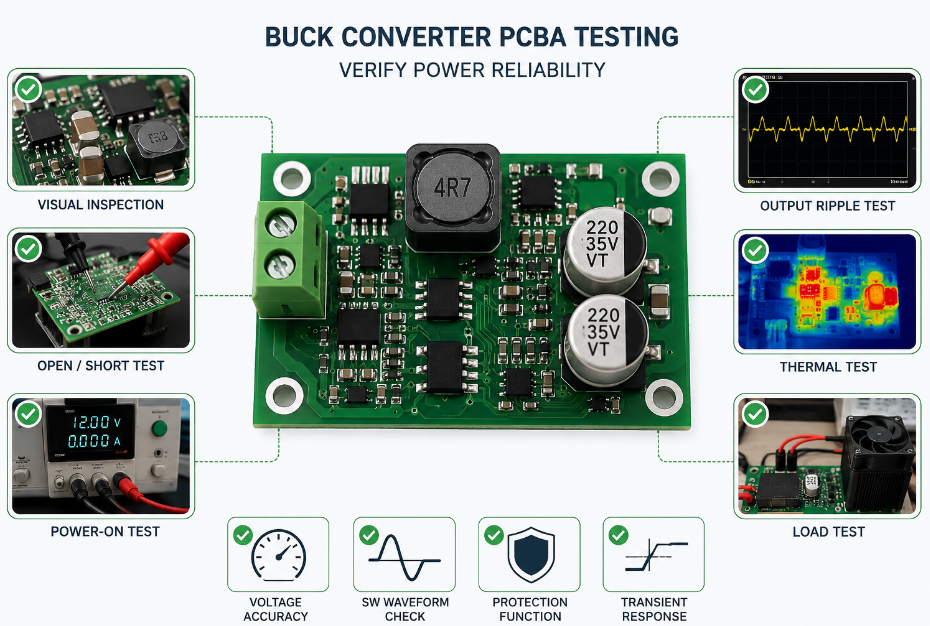
Step 6 — Functional and Electrical Testing In-Circuit Testing (ICT), flying probe, and functional test per your test specification. Power supply output voltage, ripple, load regulation, and efficiency can all be measured and logged.

Step 7 — Digital Traceability and Shipping Our digital manufacturing system provides material and batch traceability within 5 seconds. Full shipping documentation, Certificate of Conformance, and test records accompany every order.

Wholesale and Prototype: Flexible Volume for Every Stage

One of the most common pain points for engineers is finding a PCBA partner who can serve them cost-effectively across all stages of a product’s lifecycle — from the first 5-piece engineering sample to a 10,000-piece production run. EBest Circuit is purpose-built to support this entire journey.

  • Prototype (1–10 pcs): Minimum 1 piece. Rapid prototyping with DFM engineering support. Designed for design validation and debugging loops.
  • Small Batch (10–500 pcs): Pre-production validation builds. Fixed setup costs spread across units. Suitable for crowdfunding fulfillment or pilot programs.
  • Volume / Wholesale (500+ pcs): Competitive unit pricing with full SMT line utilization. Long-term blanket order contracts available for supply chain security.

Our standard full-service PCBA lead time is 1.5 weeks (approximately 10–12 business days) from the date your Gerber files, BOM, and purchase order are confirmed. This covers PCB fabrication, component procurement (assuming stock availability), SMT assembly, AOI, and final testing. Express options are available for urgent projects.

Certifications and Quality System

Quality is a documented, audited, and continuously improved system. EBest Circuit holds the following certifications, each maintained through regular third-party audits:

  • ISO 9001:2015 — General quality management system
  • ISO 13485:2016 — Medical device supply chain quality
  • IATF 16949:2016 — Tier 1 automotive supplier process control and PPAP documentation
  • AS9100D — Aerospace and defense supply chain requirements
  • IPC-A-610 — PCB assembly workmanship standard
  • RoHS / REACH — Environmental compliance

The IATF 16949 certification means our processes meet the highest standards for process control in the automotive industry. The AS9100D certification covers aerospace and defense supply chain requirements. ISO 13485 ensures our quality system is compliant for medical device supply chains — all relevant certifications for engineers who need their power supply boards to meet the most demanding end-market requirements.

Our digital workshop management system enables real-time tracking of material lots, production batches, and individual board serial numbers. In the event of a field return or audit, full manufacturing history can be retrieved in under 5 seconds — an essential capability for automotive and medical customers.

Why 1,800+ Engineers Choose EBest Circuit?

20 years of specialized PCBA history. EBest Circuit (Best Technology) has been focused on PCB fabrication and PCBA assembly for over two decades. We have supported more than 10,000 engineers and 1,800+ customers worldwide across medical, automotive, industrial, aerospace, and consumer electronics sectors.

The 1 Business Partner + 3-Engineer Technical Team model. Every new project is assigned a dedicated team: one experienced business partner who manages communication and timelines, plus a three-engineer technical team comprising a 20-year R&D engineer, a PCB process specialist, and a PCBA assembly engineer. This means:

  • Engineering questions are answered by engineers, not by a sales representative reading from a spec sheet.
  • DFM findings are reviewed by a multi-discipline team, not a single generalist.
  • Your project manager has technical authority to approve or flag issues without internal escalation delays.
  • Communication is consolidated — one contact, no information loss between departments.

Own factory with direct quality control. We own both our PCB fabrication facility and our PCBA assembly line. This vertical integration gives us direct control over every substrate that goes into your board — nothing is delegated to a sub-contractor we cannot audit. At the same time, our 1,000+ component supply chain partners ensure broad BOM coverage and transparent pricing for wholesale orders.

If you are ready to move your power supply design from schematic to production, our engineering team is ready to review your files and provide a technical assessment and competitive pricing — typically within 24 hours. Just feel free to send your Gerber files, BOM, and project requirements to sales@bestpcbs.com.

Our team of dedicated engineers — not automated forms — will personally review your specifications and respond with a tailored recommendation. Whether you need a 5-piece prototype to validate your design or a 10,000-piece wholesale production run to meet a launch deadline, EBest Circuit has the process capability, certifications, and engineering depth to deliver on time.

FAQs About Custom PCB Power Supply

What is the minimum order quantity for a custom PCB power supply?

EBest Circuit supports prototype orders from as little as 1 piece. There is no minimum order quantity restriction for engineering samples. Wholesale pricing tiers begin at approximately 500 pieces, with the most competitive rates available from 5,000 pieces and above.

How long does PCBA assembly take for a custom power supply?

Our standard full-service PCBA lead time is 1.5 weeks (approximately 10–12 business days) from the date your Gerber files, BOM, and purchase order are confirmed. This includes PCB fabrication, component procurement, SMT assembly, AOI, and final testing. Rush options are available for time-critical projects.

Do you provide DFM review?

Yes — DFM review is included as a standard part of our engineering service. Every project receives a formal written DFM Pre-Screening Report before production is approved, covering Gerber verification, clearance/creepage compliance, via-in-pad review, component spacing, and BOM optimization recommendations.

Can you manufacture metal-core PCBs for high-power applications?

Yes. Our capability covers aluminum-core PCBs (alloys 1100, 1050, 2124, 5052, 6061) and copper-core PCBs for ultra-high thermal conductivity applications. Standard thermal conductivity ranges from 0.3 to 6 W/m·K, with advanced capability up to 12 W/m·K. Metal core boards support 1–6 layers in standard process (more on review).

Which certifications does EBest Circuit hold?

EBest Circuit is certified to ISO 9001:2015, ISO 13485:2016, IATF 16949:2016, and AS9100D. These certifications are maintained through regular third-party audits.

How do you ensure component authenticity for wholesale orders?

All components are sourced through 1,000+ verified supply chain partners. For aerospace and medical builds, active counterfeit screening is performed including X-ray inspection and full lot traceability. Certificates of Conformance are provided with every shipment.

You may also like

Custom Motherboard PCB Manufacturing: From Layout Optimization to Full PCBA

May 7th, 2026

Custom MotherboardPCBs are the backbone of high-end electronics, serving as the central, custom-designed printed circuit board that integrates and connects all critical components within a system. This article will cover the entire journey of creating a custom motherboard, from initial layout design and rigorous verification to prototype fabrication, mass production requirements, and how to select the right manufacturing partner to ensure performance and reliability.

Are you grappling with the complex challenges of bringing a bespoke motherboard from concept to a reliable, high-performance product?

  • Struggling with signal integrity issues like crosstalk and EMI in dense, multi-layer layouts, leading to unstable prototype performance.
  • Facing costly delays and re-spins due to overlooked Design for Manufacturability (DFM) errors that only surface during PCBA assembly.
  • Dealing with the headache of sourcing long-lead-time or obsolete components, which stalls your entire project timeline.
  • Worrying about inconsistent quality and yield between your prototype run and the final mass production batch.
  • Feeling lost without responsive technical support when urgent design tweaks or production issues arise mid-project.

As a professional PCBA manufacturer, EBest Circuit (Best Technology) addresses these challenges directly with tailored solutions:

  • Our 20-year experienced engineering team provides in-depth DFM analysis and layout optimization advice specifically for complex, multi-layer motherboard designs to preempt signal and thermal issues.
  • We deliver a comprehensive DFM pre-screening report and BOM optimization list before fabrication, catching potential assembly faults early to save time and cost.
  • Our one-stop service integrates PCB fabrication with component sourcing from a network of 1,000+ vetted partners, ensuring authentic parts and streamlined supply chain management.
  • We maintain consistent, certified processes from prototype to mass production, supported by in-house PCB and PCBA factories for end-to-end quality control.
  • Our ‘1+3’ Support Model ensures elite project care, pairing you with one dedicated account manager and three specialist engineers for rapid, expert solutions from prototype to production.

EBest Circuit (Best Technology) is a professional PCB and PCBA manufacturer with over 20 years of expertise in serving the high-end electronics industry. Our strength lies in a full turnkey solution, where our seasoned engineering team provides DFM analysis and process adaptation from the start. We support everything from PCB design and fabrication—including advanced boards like heavy copper, HDI, and RF PCBs—to component sourcing, PCBA assembly, and full box build. Holding certifications like ISO 9001, IATF 16949, AS9100D, and ISO 13485, our in-house facilities and digital workshop enable precise batch traceability and rapid iteration for both prototypes and small-batch production. With a history of serving over 1,800 clients, we are committed to delivering comprehensive, high-quality solutions with a focus on on-time delivery. For inquiries, pls feel free to contact us at sales@bestpcbs.com.

 custom motherboard

What Is a Custom Motherboard PCB in High-End Electronics?

A custom motherboard​ PCB is the central, application-specific circuit board engineered to be the core of a dedicated electronic system, unlike standard off-the-shelf models. In high-end applications—from advanced gaming rigs and high-performance computing clusters to specialized industrial controllers and medical imaging systems—these boards are tailored to meet exact spatial, thermal, electrical, and functional requirements. This section explores the defining characteristics and critical role of a custom PC motherboard​ in pushing the boundaries of technology.

The value of a custom built motherboard​ lies in its optimized integration. Key specifications typically include:

  • High Layer Count:​ Often 8 layers or more (capable up to 32 layers for FR4) to accommodate complex power and signal routing, reducing noise and crosstalk.
  • Controlled Impedance:​ Critical for high-speed data buses (e.g., DDR memory, PCIe). Tolerances are tight, typically ±10% for values >50Ω and ±5Ω for values ≤50Ω.
  • Advanced Materials:​ Use of High-Tg FR4 (e.g., Tg ≥170°C), low-loss laminates for RF sections, or even Metal Core PCBs (MCPCBs) for thermal management in power-intensive areas.
  • Fine Features:​ Minimum trace/space can go down to 2.5/2.5 mil for inner layers and 3/3 mil for outer layers (with 1 oz copper), supporting high-density interconnects (HDI).
  • Multiple Surface Finishes:​ Selection of ENIG, ENEPIG, or hard gold for edge connectors (gold fingers) based on durability and signal integrity needs.
  • Rigorous Testing:​ 100% electrical testing (E-test) and flying probe testing for prototypes are mandatory to ensure connectivity and function before PCBA.

The custom motherboard​ is therefore not just a carrier of components but a precision-engineered substrate that determines the ultimate performance, reliability, and scalability of the entire system. Its design and fabrication set the foundation for all subsequent assembly and integration steps.

How Are Custom Motherboards Formed From PCB and PCBA?

The formation of a functional custom motherboard​ is a two-stage symphony: first, the fabrication of the bare Printed Circuit Board (PCB), and second, the assembly of components onto it (PCBA). The PCB serves as the foundational platform with its intricate copper tracings, while the PCBA process populates this platform with ICs, connectors, and passive components, breathing life into the design. Understanding this seamless transition is key to planning a successful custom motherboard​ project.

The journey from a PCB panel to a ready-to-use custom built motherboard​ involves a detailed, interconnected workflow:

  • PCB Fabrication:​ This starts with the manufactured bare board. For a complex motherboard, this involves multi-layer lamination, precision drilling of micro-vias (laser drill capability down to 0.1mm), and plating. Key outputs are the physical boards meeting all specified impedance, thickness, and finish requirements.
  • Component Procurement & Kitting:​ Parallel to or after PCB fab, all components from the BOM are sourced. A reliable manufacturer uses authorized distributors to avoid counterfeits and can provide BOM optimization advice.
  • SMT Assembly:​ Surface Mount Technology lines place microscopic components (down to 01005 size) using high-precision pick-and-place machines. A full nitrogen reflow oven ensures perfect solder joints for BGA packages with pitches as fine as 0.25mm.
  • THT Assembly & Conformal Coating:​ Through-hole components (like large connectors or power sockets) are inserted, often via selective or wave soldering. Conformal coating may be applied for environmental protection.
  • Inspection & Testing:​ This is critical. Automated Optical Inspection (AOI) and X-ray (for BGA joints) check for assembly defects. In-circuit Test (ICT) or Flying Probe Test verifies electrical performance. For motherboards, Functional Test (FCT) simulating real operation is often required.
  • Programming & Boxing:​ Firmware is loaded onto onboard memory. Finally, the assembled PCBA may be integrated into an enclosure or delivered as a complete system (box build).

This integrated PCB and PCBA​ flow underscores the need for a manufacturer that controls both processes. Any disconnect between the board fabrication tolerances and the assembly process windows can lead to failures, making a one-stop, turnkey service provider like EBest Circuit (Best Technology) a strategic advantage for custom motherboard​ realization.

How to Optimize Your Layout for a Custom Motherboard PCB?

Layout optimization is the strategic placement and routing of components and traces on a custom motherboard PCB​ to achieve optimal electrical performance, thermal management, manufacturability, and reliability. A poorly optimized layout can doom even the most well-conceived schematic, leading to signal integrity nightmares, overheating, and assembly failures. For a custom motherboard​ that often integrates high-speed processors, memory, and various I/Os, this phase is arguably the most critical in the design cycle.

Optimizing a custom motherboard layout​ requires balancing electrical and physical constraints. Here are key actionable strategies:

  • Stack-up Planning:​ Define your layer stack-up early with your manufacturer. For an 8-layer board, a common stack like [Sig-Gnd-Pwr-Sig-Sig-Pwr-Gnd-Sig] provides good signal return paths. Use controlled dielectric materials (e.g., Dk ~4.2 for standard FR4, lower for high-speed sections) and aim for target impedance values (e.g., 50Ω for single-ended, 100Ω for differential pairs).
  • Power Distribution Network (PDN):​ Use dedicated power and ground planes. For high-current rails (like CPU Vcore), calculate required copper weight (e.g., 2 oz or more) and use multiple vias for current sharing. Implement proper decoupling capacitor placement—use a mix of bulk, ceramic, and high-frequency caps close to power pins.
  • High-Speed Signal Routing:​ Route critical signals (e.g., DDR, PCIe) with length matching (tolerance within ±5 mils for differential pairs) and maintain consistent impedance. Provide adequate spacing (3x trace width minimum) to minimize crosstalk. Avoid splitting reference planes beneath high-speed traces.
  • Thermal Management:​ Identify hot components (CPUs, FPGAs, VRMs) and plan for thermal relief. Incorporate thermal vias under pads to conduct heat to inner copper layers or a metal core. In designs with localized high heat, consider specifying a Metal Core PCB (MCPCB) section with thermal conductivity of 1.5-3.0 W/m·K.
  • DFM-Centric Design:​ Adhere to your manufacturer’s capabilities. For example, maintain a minimum solder mask bridge of 6-8 mil, a minimum annular ring of 8 mil for vias, and trace/space rules that match your chosen copper weight (e.g., 5/7 mil for 2 oz outer layer). Avoid acute angles in traces.

By methodically applying these principles, you transform a schematic into a manufacturable, high-performance board layout. Partnering with a manufacturer that offers custom motherboard design​ review services can provide invaluable feedback at this stage, catching potential issues before they are etched in copper, saving significant time and cost.

Why Is Custom Motherboard Design Verification Critical for PCBA?

Custom motherboard design​ verification is a rigorous, multi-faceted checking process that occurs after layout completion but before committing to fabrication. It is critical for PCBA because it identifies and rectifies design flaws that are far cheaper to fix in software than on physical boards. A single uncaught error—a missed connection, an incorrect footprint, or a violated design rule—can lead to non-functional assemblies, costly rework, and project delays, undermining the entire custom motherboard​ project.

A comprehensive verification strategy for a custom PC motherboard​ should include the following checks:

  • Electrical Rule Check (ERC):​ Validates logical connectivity against the schematic, ensuring all nets are properly driven and terminated, and checking for floating pins or shorted outputs.
  • Design Rule Check (DRC):​ Enforces physical layout constraints provided by the manufacturer. This includes checks for minimum trace width/space (e.g., 4/4 mil for normal FR4), drill-to-copper clearance (≥0.18mm for through-holes), and solder mask slivers.
  • Signal Integrity (SI) & Power Integrity (PI) Simulation:​ Uses field solvers to analyze signal quality (overshoot, crosstalk, timing) on high-speed nets and to model the impedance of the Power Distribution Network, identifying voltage drop and resonance issues before building the board.
  • Thermal Simulation:​ Models the board’s thermal performance under load, identifying hotspots that may require additional cooling measures like heatsinks, thermal vias, or a different substrate material (e.g., switching to an Aluminum PCB section).
  • Design for Manufacturability (DFM) Analysis:​ A manufacturer-led review using their specific process capabilities. They check for issues like acid traps, copper slivers, inadequate annular rings, and impractical aspect ratios for plating (e.g., a maximum 8:1 aspect ratio for through-holes).
  • Design for Assembly (DFA) Analysis:​ Focuses on the PCBA phase. Checks include component spacing for soldering tool access, polarity markings, stencil aperture design for proper paste volume, and suitability of selected surface finish (e.g., ENIG for fine-pitch BGAs).

Skipping or shortening these verification steps is a high-risk gamble. A single PCBA run for a complex custom motherboard​ represents a significant investment in boards and components. Thorough verification, especially a professional DFM/DFA report from your manufacturing partner, is the most effective insurance policy to ensure your first prototype assembly has the highest chance of success, accelerating your path to a validated, production-ready design.

How Do We Fabricate Prototypes for Complex Custom Motherboards?

Fabricating prototypes for complex custom motherboards​ is a specialized service that bridges the gap between design and validation, allowing engineers to physically test and iterate their concepts. It involves manufacturing small quantities of the fully assembled board with the same care and access to advanced processes as mass production. For a custom motherboard, where cost and complexity are high, a reliable and fast prototype service is indispensable for de-risking the project before committing to volume orders.

The prototype fabrication process at a full-service manufacturer like EBest Circuit integrates several key stages:

  1. Rapid PCB Prototyping:​ The bare PCB is fabricated first. For standard FR4 motherboards, fastest service can be as quick as 24 hours for 1-2 layer boards and 48-72 hours for 4-8 layer boards. Advanced features like HDI (laser drilled 0.1mm microvias) and heavy copper (up to 20 oz) are available even for prototype quantities.
  2. Expedited Component Sourcing:​ The manufacturer procures all components, often leveraging existing distributor relationships and in-house inventory for common parts to avoid delays, even for small BOMs.
  3. Quick-Turn PCBA:​ The assembly line is set up for prototype agility. SMT lines can place fine-pitch components, and selective soldering handles THT parts. PCBA prototype lead time can be as fast as 2 days for standard assemblies.
  4. Focused Inspection & Testing:​ Each prototype board undergoes meticulous inspection. Flying Probe Testing (instead of a custom fixture) is used for 100% electrical verification. AOI and X-ray check solder joint quality, ensuring the prototype is fully testable.

Typical Prototype Lead Time Framework (for a standard 8-layer FR4 motherboard):

Process StageNormal ServiceExpedited / Fastest ServiceKey Notes
PCB Fabrication12 Days72 HoursFor boards <1 sq. meter, standard spec.
Component Sourcing3-5 Days1-3 DaysDepends on part availability.
PCBA & Testing1 Week2 DaysIncludes SMT, THT, and basic flying probe test.
Total Project Timeline~3 Weeks~1.5 WeeksWith streamlined coordination and expedited services.

Prototype fabrication is not just about speed; it’s about learning. The physical board provides invaluable data on real-world performance, thermal behavior, and assembly yield. Choosing a partner that supports both PCB prototype​ and PCBA prototype​ in one flow, with transparent communication and engineering support, turns the prototype phase into a powerful tool for refinement, ensuring your custom motherboard​ design is robust and ready for scaling.

What Are the Fabrication Requirements for a Custom PC Motherboard?

The fabrication requirements for a custom PC motherboard​ are a comprehensive set of technical specifications and standards that the bare PCB must meet to be viable for component assembly and reliable end-use. These requirements go beyond simple connectivity, encompassing electrical performance, physical durability, thermal characteristics, and precise dimensional tolerances. Clearly defining and communicating these requirements to your manufacturer is the first step to ensuring the fabricated board is a perfect match for your design intent and the subsequent PCBA process.

The specifications for a high-performance custom motherboard​ are detailed and multi-faceted. Below is a consolidated overview of key fabrication requirements, drawing from advanced PCB process capabilities.

Key Fabrication Specifications for a Complex Custom Motherboard PCB

Requirement CategorySpecification / ParameterTypical Value / RangeImportance for Motherboard
Materials & ConstructionBase MaterialHigh-Tg FR4 (≥170°C), maybe with Rogers for RF sections.Provides thermal stability during soldering and operation.
Layer Count6 to 32 layers.Accommodates complex power delivery and high-density routing.
Finished Board Thickness1.6mm ±0.16mm is common; range from 0.4mm to 6.0mm.Fits standard chassis and connector heights.
Features & TolerancesMin. Trace/Space (Inner, 1 oz Cu)2.5 / 2.5 mil (0.0635 / 0.0635mm).Enables dense routing for complex chipsets.
Min. Hole Diameter (Mechanical)8 mil (0.2mm) for HDI areas; 12 mil (0.3mm) standard.For high-density via fanout.
Hole Position Tolerance±2 mil (±0.05mm).Critical for precise component alignment during PCBA.
Impedance Control Tolerance±10% (≥50Ω), ±5Ω (<50Ω).Essential for signal integrity of high-speed interfaces.
Surface & FinishingSurface FinishENIG, ENEPIG, or Immersion Silver common.Provides flat, solderable surface for fine-pitch components.
Gold Finger (Edge Connector)Hard gold plating, thickness 0.1-1.27 µm.Ensures durability for repeated insertion/removal.
Solder Mask (LPI)Green, black, blue, etc.; Min. bridge: 6 mil.Prevents solder bridges and provides insulation.
Reliability & TestingThermal Stress3 cycles of 10 sec @ 280°C (for lead-free).Validates ability to withstand reflow soldering heat.
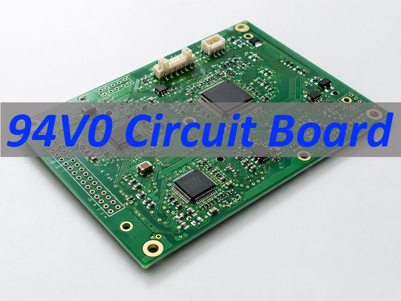
Flammability RatingUL 94V-0 compliant.Mandatory safety standard for most electronic products.
Bow and Twist≤0.75% of board diagonal length.Ensures flatness for automated PCBA and proper heatsink contact.

These requirements form a contract of quality between you and the fabricator. A manufacturer experienced in custom motherboard PCB​ production will not only meet these specs but will also proactively advise on optimal choices—for instance, recommending a specific surface finish for your BGA pitch or validating your impedance stack-up model—ensuring the fabricated board is a solid foundation for a successful, high-yield PCBA process.

How to Choose a Reliable Custom Motherboard Manufacturer for Your Project?

Choosing a reliable custom motherboard manufacturer​ is a strategic decision that impacts not only the unit cost but also the technical success, timeline, and long-term scalability of your product. The ideal partner is more than a board vendor; they are a technical collaborator with the expertise, infrastructure, and commitment to guide your complex project from design to delivered, tested assemblies. For a custom motherboard, this choice is pivotal in navigating the challenges of high-density interconnects, advanced materials, and rigorous quality demands.

Selecting the right manufacturer requires evaluating them against a set of critical criteria that go beyond a simple price quote. Consider the following checklist:

  • Technical Expertise & Support:​ Do they have a seasoned engineering team (20+ years experience) that can provide meaningful DFM/DFA analysis on your custom motherboard design? Can they advise on material selection, thermal management, and signal integrity? Look for 1-on-1 project support.
  • Process Capabilities & Certifications:​ Can their factory produce the required specs (layer count, trace/space, surface finishes, impedance control)? Verify relevant certifications: ISO 9001​ (quality management), IATF 16949​ (automotive), ISO 13485​ (medical), and AS9100D​ (aerospace) if applicable, which mandate rigorous process control.
  • Supply Chain & One-Stop Service:​ Do they offer true turnkey service (PCB + components + PCBA + test)? A strong network of 1,000+ component suppliers is vital to manage shortages and ensure authentic parts. In-house PCB and PCBA factories prevent finger-pointing and improve communication.
  • Prototype & Volume Flexibility:​ Can they efficiently handle both your initial prototype/small-batch needs (for fast R&D iteration) and seamlessly scale to mass production while maintaining consistency? Ask about their “digital workshop” capabilities for traceability.
  • Quality Assurance & Testing Infrastructure:​ What inspection and test equipment do they have in-house? Look for AOI, X-ray, Flying Probe Testers, and functional test beds. A commitment to IPC standards​ for PCB and PCBA is non-negotiable for reliability.
  • Communication & Project Management:​ Is their response time fast (e.g., within 12 hours)? Do they provide online Work-in-Progress (WIP) updates? Transparent and proactive communication is essential for managing a complex project.

The best motherboard customer service​ is characterized by partnership, not just transaction. It means having an expert you can call when a design issue arises, receiving proactive updates on your build, and trusting that quality is ingrained in their process. By thoroughly vetting potential partners against these criteria, you align with a manufacturer that reduces risk, adds value, and becomes a key enabler for your custom motherboard​ project’s success.

How Does Motherboard Customization Ensure Better Performance?

Motherboard customization​ is the process of tailoring the PCB’s electrical, physical, and thermal properties to the exact needs of a specific application, which directly translates to superior performance compared to using a generic, off-the-shelf board. This optimization impacts every aspect of the system: speed, power efficiency, thermal behavior, reliability, and form factor. For demanding applications, a custom built motherboard​ is not a luxury but a necessity to achieve performance benchmarks and gain a competitive edge.

The performance benefits of a custom PC motherboard​ are realized through targeted design choices across several domains:

  • Optimized Signal Integrity and Speed:​ Customization allows for precise control over the PCB stack-up, dielectric materials, and trace geometry. This enables perfect impedance matching for high-speed signals (e.g., DDR5, PCIe 5.0), minimizing reflections and losses. You can use low-loss laminates (Df < 0.005) in critical paths, which a standard FR4 board does not offer, allowing for higher data rates and lower bit error rates.
  • Enhanced Thermal Management:​ A one-size-fits-all motherboard has generic thermal design. Customization lets you integrate direct thermal solutions. For example, you can specify a thicker copper plane (e.g., 3 oz) under a high-power CPU, incorporate an array of thermal vias to an internal ground plane, or even design a section as a Metal Core PCB (MCPCB) with a thermal conductivity of 2.0-3.0 W/m·K to act as an integrated heatsink, dramatically lowering junction temperatures.
  • Superior Power Delivery:​ Custom power planes can be designed with the exact copper weight and shape needed for each voltage rail, reducing DC resistance (Rdc) and voltage drop. This ensures stable power to sensitive components like FPGAs and GPUs, even under transient loads, preventing throttling and ensuring consistent performance.
  • Form Factor and Component Optimization:​ The board can be shaped to fit a unique enclosure, and components can be placed for optimal mechanical and electrical interaction. This reduces parasitic inductance and capacitance from long traces, improves EMI performance by allowing for better shielding strategies, and can even reduce the overall part count by integrating functions, leading to higher reliability.

In essence, motherboard customization​ moves the design from a compromise-based generic solution to a purpose-engineered platform. It allows engineers to make deliberate trade-offs that favor the most critical performance parameters of their specific application, whether that’s raw compute speed, power efficiency in a battery-operated device, or rugged reliability in an industrial setting. This tailored approach is what unlocks the full potential of the components mounted on it.

Why Do Complex Projects Need the Best Motherboard Customer Service?

Complex projects involving custom motherboards​ inherently carry high technical risk, significant investment, and tight schedules. The best motherboard customer service​ is the essential human and procedural interface that actively manages this risk, provides expert guidance, and ensures smooth project execution. It transforms a manufacturing transaction into a collaborative partnership, where the manufacturer’s team acts as an extension of your own, providing support that is proactive, knowledgeable, and responsive to the unique challenges of a sophisticated custom motherboard​ build.

Outstanding customer service for a complex motherboard project manifests in several critical, tangible ways:

  • Front-Loaded Technical Collaboration (Pre-Sales):​ Before any order is placed, the service team facilitates deep-dive technical reviews. Their engineers provide a detailed DFM report, not just flagging errors but offering solutions—like suggesting changing a via pad size from 8 mil to 10 mil for better reliability, or recommending an alternative surface finish for a challenging BGA. This prevents costly mistakes from ever reaching production.
  • Proactive Supply Chain Management:​ For a custom motherboard​ with a large, complex BOM, component sourcing is a minefield. The best service includes a dedicated procurement specialist who proactively communicates about part availability, suggests alternates for end-of-life or long-lead items, and provides a consolidated, optimized BOM list, de-risking your supply chain from the start.
  • Real-Time Project Visibility & Communication:​ You are not left in the dark. A digital portal or regular WIP updates show you the status of your boards at every stage—from PCB lamination and drilling to SMT assembly and testing. If a minor issue arises (e.g., a solder paste issue on the line), you are informed immediately with a solution, not after the fact.
  • Rapid-Response Problem Solving:​ When an unexpected challenge occurs—a last-minute engineering change order (ECO), a test failure that needs diagnostics—the service team provides fast, expert-level troubleshooting. They have direct access to the factory floor and engineering teams to investigate and resolve issues within hours, not days, keeping your project on track.
  • Seamless Transition from NPI to Mass Production:​ The team that guided your prototype ensures all learnings and specifications are perfectly handed over to the volume production group. They manage the transition, ensuring there are no surprises in quality or process when you scale up your order.

For a complex project, this level of service is not a premium add-on; it is a core component of project success. The best custom motherboard manufacturer​ understands that their value lies as much in their knowledge, communication, and support as in their machinery. This partnership minimizes stress, accelerates time-to-market, and provides the confidence that your intricate, high-stakes project is in capable hands from the first design file to the final shipped unit.

To sum up, custom motherboard​ PCBs are the engineered heart of high-performance electronic systems, where tailored design and precision manufacturing converge to unlock specific application potential. This article has detailed the journey from optimized layout and critical verification through prototype fabrication and the stringent requirements of mass production, underscoring the importance of choosing a manufacturing partner that acts as a true collaborator.

EBest Circuit (Best Technology) brings over 20 years of PCB and PCBA expertise to this complex field. Our in-house engineering team provides deep DFM analysis for your custom motherboard design, while our one-stop turnkey service—encompassing advanced PCB fabrication, robust component sourcing, and high-mix PCBA assembly—ensures a seamless, accountable process from prototype to volume production. Supported by relevant quality certifications and a digital workshop for full traceability, we are equipped to be your reliable partner in bringing high-performance, reliable custom motherboards to market. Pls feel free to contact our team anytime to discuss your project requirements at sales@bestpcbs.com.

FAQs About Custom Motherboard

Q1: What is the typical lead time for a prototype of a custom motherboard, and can it be expedited?

A: The lead time for a custom motherboard prototype​ depends on complexity. For a standard 8-layer FR4 design (<1 sq. meter), normal PCB fabrication is about 12 days, with PCBA adding roughly a week. However, with expedited services, the PCB can be built in 72 hours, and fast-turn PCBA can be completed in 2 days, bringing the total project timeline to approximately 1.5 weeks. Manufacturers like EBest Circuit offer such rush services to help accelerate R&D validation cycles.

Q2: What are the key DFM (Design for Manufacturability) checks I should perform on my custom motherboard design before sending it out?

A: Beyond standard ERC/DRC, focus on manufacturer-specific process limits. Key checks include: ensuring trace/space and annular ring sizes meet their standard (e.g., 5/7 mil for 2 oz copper), verifying hole-to-copper clearance (≥0.18mm), avoiding excessive copper in flex areas to prevent cracking, and confirming your impedance stack-up model is achievable with their materials. The most effective step is to request a formal DFM report from your chosen manufacturer, as they will apply their exact equipment and process tolerances to your design.

Q3: How do you handle component sourcing, especially for obsolete or hard-to-find parts on a custom PC motherboard BOM?

A: A reputable turnkey manufacturer manages this through a multi-pronged approach. They first source from a network of authorized distributors to guarantee authenticity. For obsolete parts, their procurement team will identify and suggest qualified, form-fit-function equivalent alternates. They can also leverage in-house inventory of common components. Providing your BOM early allows them to initiate sourcing in parallel with PCB fabrication, mitigating lead time risks. Always ask for a component sourcing report before production begins.

Q4: What is the advantage of using a Metal Core PCB (MCPCB) section in a custom motherboard design?

A: Integrating an MCPCB section, typically aluminum-based, is a powerful thermal management strategy for custom motherboard customization. The metal core acts as an integrated heatsink, conducting heat away from high-power components like VRMs or processors much more efficiently than standard FR4 (thermal conductivity of 1.5-3.0 W/m·K vs. ~0.3 W/m·K). This can lower component operating temperatures significantly, improving reliability and performance, and potentially eliminating the need for bulky external heatsinks in some areas, allowing for a more compact design.

Q5: Can you support both small-batch prototyping and later mass production for the same custom motherboard design?

A: Yes, the best manufacturers are equipped for this full lifecycle support. They use the same certified processes and equipment lines for both prototyping and volume runs, ensuring consistency. The transition is managed by the same engineering and customer service team, who carry over all the learnings and optimized parameters from the prototype phase. This seamless handoff guarantees that the performance and quality you validated in your prototypes are maintained in mass production, which is critical for a custom motherboard manufacturer​ relationship.

You may also like

Small Printed Circuit Board | No MOQ & Fast-Turn Assembly Services

May 6th, 2026

A small printed circuit board​ serves as the miniature backbone for compact electronic devices, enabling high-density interconnections in limited spaces. This article explores the technical nuances, manufacturing standards, and cost factors associated with producing these intricate assemblies.

Are you struggling with the unique challenges that come with miniaturized electronics?

  • My design has tiny components, but I keep getting poor yields due to soldering defects.
  • We only need 5 or 10 pieces for the prototype, yet every supplier demands a massive MOQ.
  • It is frustrating when signal interference ruins my RF performance in a dense layout.
  • I cannot find a factory that understands the precision needed for micro-vias and fine traces.
  • Getting a clear and accurate price for a small batch is nearly impossible with all the hidden fees.

As a professional PCBA manufacturer, we address these challenges directly:

  • We deploy precision SMT placement machines to handle miniature components reliably.
  • Our flexible production lines support printed circuit board small quantity runs with no MOQ.
  • We design and integrate custom printed circuit board small rf shielded enclosures.
  • Our 20-year engineering team specializes in small printed circuit board fabrication.
  • We provide transparent quotations and a detailed small printed circuit board pricelist upfront.

With two decades of experience, EBest Circuit (Best Technology) has become a trusted partner for engineers worldwide. Our strengths lie in combining deep technical expertise with responsive manufacturing capabilities. We offer a true one-stop service covering PCB fabrication, component sourcing, assembly, and functional testing. Backed by ISO 9001, IATF 16949, ISO 13485 and AS9100D certifications, we ensure quality compliance across industries. Our in-house facilities, coupled with a supply chain of over 1,000 partners, allow us to manage everything from prototypes to small-batch production efficiently. This infrastructure supports rapid R&D iteration while maintaining full traceability through our digital workshop system. For inquiries, pls feel free to contact us at sales@bestpcbs.com.

Small Printed Circuit Board

What is Small Printed Circuit Board?

A small printed circuit board typically refers to two distinct but interlinked concepts in the electronics industry: miniaturized physical dimensions and low-volume production runs.

Physically, it is a high-density interconnect (HDI) board engineered to fit into compact devices like wearables, medical sensors, and IoT modules. These boards demand extreme precision, often featuring line widths and spaces as fine as 2mil (0.05mm) and laser-drilled micro-vias of 0.1mm. Because of their tiny footprint, they require specialized fabrication techniques to ensure signal integrity and thermal stability.

From a manufacturing perspective, “small” also pertains to small-batch or prototype assembly. This service is vital for engineers who need a limited quantity (often 5 to 100 units) to validate a design before scaling to mass production. At EBest Circuit (Best Technology), we bridge the gap between these two definitions by providing high-precision, small-sized boards with No MOQ requirements, supporting your project from the first micro-prototype to full-scale market deployment.

What are the small holes in printed circuit boards called? (Vias & Through-holes)

Understanding the terminology and function of plated holes is fundamental when designing a small printed circuit board. These features are not merely drilled openings; they are conductive pathways that determine the electrical integrity and layer transitions of your circuit. Properly specifying these elements ensures signal continuity and mechanical stability in high-density designs.

TypeFunctionSpecs / Notes
Through-HoleTop-to-bottom layer connectionFor THT parts; min. drill Ø ~0.2mm.
Micro-viaAdjacent layer connection (HDI)Laser-drilled; often copper/resin-filled.
Blind ViaOuter to inner layer connectionNon-through-hole; depth/diameter ratio critical.
Buried ViaInternal layer connection onlyHidden within board; requires extra lamination.
Thermal ViaHeat transfer from componentsUnder thermal pads (e.g., QFN); aids cooling.
  • Aspect Ratio:​ Maintain an aspect ratio (board thickness / hole diameter) of 8:1 or less for reliable plating.
  • Annular Ring:​ Ensure the copper pad surrounding the hole is at least 0.05mm to prevent breakout during drilling.
  • Via-in-Pad:​ Requires plugging and capping to prevent solder wicking; common in small printed circuit board layouts.
  • Tenting Vias:​ Covering vias with solder mask to prevent solder paste from entering the hole during reflow.

Selecting the correct via structure is essential for optimizing space and performance in your small printed circuit board. By aligning your design choices with fabrication capabilities, you minimize the risk of open circuits and manufacturing delays.

Small Printed Circuit Board

Key Components and Design: Small Printed Circuit Board Capacitors and Layout

Component selection and placement are critical in constrained layouts, especially regarding small printed circuit board capacitors. These passive components influence everything from power integrity to signal timing, requiring careful consideration during schematic design and layout phases. A well-executed plan prevents noise coupling and ensures stable operation.

  • Capacitor Types:​ Choose NP0/C0G for high-frequency stability and X7R/X5R for bulk decoupling based on dielectric needs.
  • Package Size:​ Common compact packages include 0201 (0.6mm x 0.3mm) and 0402 (1.0mm x 0.5mm) for dense placement.
  • Placement Rules:​ Place decoupling capacitors as close as possible to the power pins of ICs to minimize loop inductance.
  • Thermal Relief:​ Use appropriate pad geometry to avoid tombstoning during reflow soldering of small parts.
  • Land Pattern:​ Follow IPC-7351 standards for footprint creation to ensure compatibility with automated assembly.
  • BOM Optimization:​ Our engineering team reviews your bill of materials to suggest second-source components for better availability.
ParameterTypical Value / GuidelineImpact on Design
ESR (Equivalent Series Resistance)< 20 mΩ for low-noise applicationsAffects power supply ripple and transient response.
Voltage RatingAt least 150% of operating voltagePrevents capacitor failure under surge conditions.
Pad-to-Pad Clearance≥ 0.1mm for 0201 componentsEnsures solder bridging does not occur during assembly.

Working with experienced assemblers helps navigate the trade-offs between component size, cost, and reliability. Proper layout techniques guarantee that even the smallest capacitors perform their intended function without compromising the overall board integrity.

Solving Interference: Printed Circuit Board Small RF Shielded Enclosures

Radio Frequency (RF) designs are particularly susceptible to Electromagnetic Interference (EMI), making shielding a necessity for sensitive circuits. Incorporating printed circuit board small rf shielded enclosures protects vulnerable components from external noise and contains emissions within regulatory limits. This approach is vital for wireless modules operating in the MHz to GHz range.

  • Shielding Can Types:​ Use stamped metal cans (e.g., nickel-plated copper) soldered directly to the PCB ground plane.
  • Material Selection:​ Choose materials like cold-rolled steel or brass for optimal magnetic and electric field attenuation.
  • Ventilation & Heat:​ Design enclosures with perforations or gaps sized significantly smaller than the wavelength of interest.
  • Grounding Strategy:​ Ensure the shield connects to a low-impedance ground path to effectively sink induced currents.
  • Coaxial Transitions:​ Route RF signals through the shield wall using filtered connectors or feedthrough capacitors.
Frequency RangeRecommended Shield MaterialTypical Attenuation
100 MHz – 1 GHzNickel-Silver Alloy40 – 60 dB
1 GHz – 10 GHzTin-Plated Steel60 – 80 dB
> 10 GHzSolid Copper with Gaskets> 90 dB

Effective shielding requires a holistic view of the design, considering both mechanical and electrical interactions. By integrating enclosure design early, you prevent costly re-spins and ensure compliance with FCC or CE standards.

Industry Standards for Small Printed Circuit Board Fabrication and Factories

Adhering to recognized industry standards separates hobby-grade work from professional manufacturing. Reputable small printed circuit board factories operate under strict quality management systems to deliver consistent results. Understanding these benchmarks helps you vet potential suppliers and align expectations.

  • IPC-A-600:​ Acceptability of Printed Boards—defines criteria for visual inspection of base PCBs.
  • IPC-A-610:​ Acceptability of Electronic Assemblies—classifies solder joint quality (Class 2 vs. Class 3).
  • ISO 9001:​ Quality Management Systems ensuring process control and continuous improvement.
  • IATF 16949:​ Automotive-specific standard requiring APQP, PPAP, and FMEA documentation.
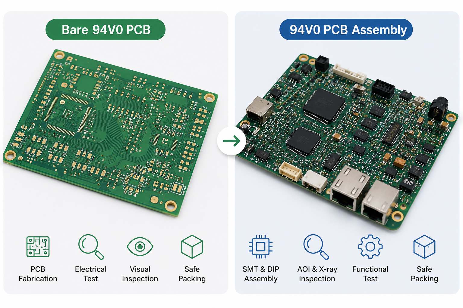
  • AS9100D:​ Aerospace standard emphasizing safety, reliability, and configuration management.
CertificationPrimary FocusBenefit for Customer
ISO 13485Medical DevicesEnsures traceability and biocompatibility controls.
UL CertificationSafety ComplianceRecognized safety mark for North American markets.
RoHS / REACHEnvironmental ComplianceGuarantees restriction of hazardous substances.

Partnering with a factory that holds these certifications provides assurance that your product will meet the rigorous demands of its target application. It reflects a commitment to process discipline and risk mitigation.
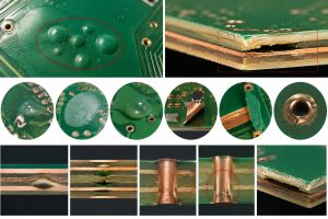
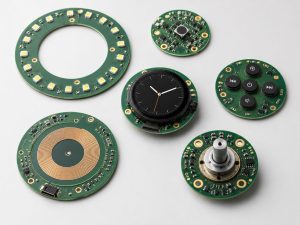
Why Opt for Printed Circuit Board Small Quantity Assembly Services?

Engineers frequently face the dilemma of needing professional assembly for limited runs without committing to mass production volumes. Printed circuit board small quantity assembly services bridge this gap, offering the precision of high-volume lines with the flexibility required for R&D. This model accelerates development cycles and reduces time-to-market.

  • Rapid Prototyping:​ Quickly validate design concepts before investing in expensive tooling.
  • Lower Financial Risk:​ Avoid tying up capital in large inventory batches that may become obsolete.
  • Design Iteration:​ Easily incorporate changes between builds based on test feedback.
  • Access to Technology:​ Utilize advanced processes like laser drilling and X-ray inspection on small lots.
  • Simplified Logistics:​ Manage a single purchase order instead of separate contracts for PCB and assembly.

This approach empowers engineering teams to fail fast, learn quickly, and refine their products efficiently. It is an indispensable strategy for startups and established companies alike.

Finding the Right Partner: Small Batch Printed Circuit Board Assembler Benefits

Selecting a competent small batch printed circuit board assembler goes beyond comparing price quotes; it involves evaluating technical support and responsiveness. The right partner acts as an extension of your engineering team, contributing insights that improve manufacturability and yield.

  • DFM Analysis:​ Receives a free Design for Manufacturability report highlighting potential assembly issues.
  • Supply Chain Access:​ Leverages established relationships with authorized distributors for genuine components.
  • Flexible Scheduling:​ Accommodates urgent changes and rush orders without derailing production flow.
  • Technical Consultation:​ Provides direct access to senior process engineers for troubleshooting assembly defects.
  • Quality Documentation:​ Delivers full inspection reports, including AOI, X-ray, and flying probe data.

These benefits compound over the lifecycle of a project, resulting in higher quality products and smoother production ramp-ups. A collaborative relationship fosters innovation rather than simply executing instructions.

Production Flexibility: The Advantages of Small Run Printed Circuit Boards

The ability to order small run printed circuit boards provides unparalleled agility in today’s fast-paced electronics market. This flexibility allows companies to test multiple design variants simultaneously or produce limited edition products without excessive waste. It aligns manufacturing output precisely with demand.

  • NPI Support:​ New Product Introduction flows smoothly from design to production with minimal lead time.
  • Inventory Management:​ Just-in-Time (JIT) production reduces warehousing costs and minimizes excess stock.
  • Customization:​ Enables niche or specialized versions of a product without retooling an entire line.
  • Cost Efficiency:​ Spreads development costs over several small runs instead of one large, risky investment.
  • Quick Turnaround:​ Many providers offer 24-hour or 48-hour build cycles for simple small run printed circuit boards.

Embracing this production model future-proofs your operations against fluctuating market demands. It transforms manufacturing from a rigid constraint into a strategic advantage.

While we excel in miniaturized designs—supporting ultra-fine line/space down to 2mil/2mil (0.05mm) and minimum laser drill sizes of 0.1mm—our capabilities are not limited to small batches. Once your prototype is validated, our fully automated production lines are equipped to scale up to high-volume mass production. We seamlessly transition your project from initial R&D to large-scale supply, maintaining the same rigorous IATF 16949 and ISO standards throughout the product lifecycle.
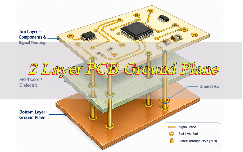
How much does it cost for small printed circuit board?

Determining how much does it cost for small printed circuit board projects depends on a matrix of variables rather than a fixed unit price. While simple two-layer boards might cost a few dollars, complex multi-layer assemblies can increase exponentially. Understanding these drivers helps you budget accurately and identify cost-saving opportunities.

  • Layer Count:​ Each additional layer adds processing steps; a 4-layer board costs more than a 2-layer board.
  • Material Type:​ Standard FR-4 is economical, whereas Rogers or polyimide materials command premium prices.
  • Surface Finish:​ ENIG (Electroless Nickel Immersion Gold) costs more than HASL but offers superior planarity.
  • Quantity:​ Economies of scale apply; the per-unit cost drops significantly as volume increases.
  • Assembly Complexity:​ High component density and fine-pitch parts require more precise placement and inspection.
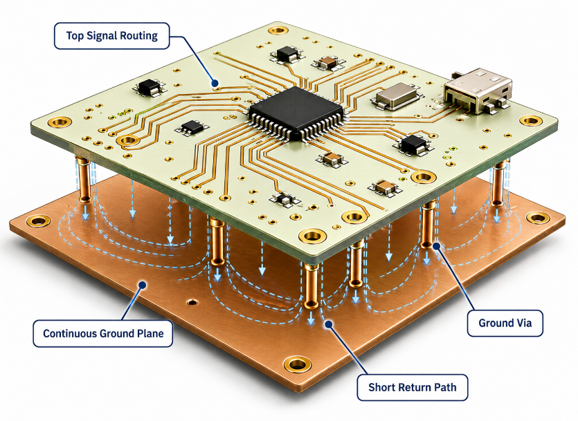
FactorLow-Cost ScenarioHigh-Cost Scenario
Layers2 Layers8+ Layers (HDI)
Board Size50mm x 50mm100mm x 100mm
Components20 SMD (all 0805+)150 Mixed (QFN, BGA)
Turnaround2 Weeks3 Days (Expedited)
Estimated Cost15–30 per unit120–250 per unit

Always request a detailed breakdown rather than a lump-sum quote to understand where your money is going. This transparency allows for informed decisions about value engineering.

Understanding the Small Printed Circuit Board Pricelist and Cost Factors

A comprehensive small printed circuit board pricelist itemizes every charge, eliminating surprises later in the process. Scrutinizing this document reveals the manufacturer’s transparency and helps you compare bids objectively. Key line items typically include engineering fees, tooling charges, and recurring production costs.

  • Tooling / Setup Fee:​ One-time charge for creating Gerber files, generating stencils, and programming pick-and-place machines.
  • Raw Material Cost:​ Calculated based on panel utilization; larger panels reduce per-board cost.
  • Labor Cost:​ Reflects the complexity of assembly; hand-soldering or manual rework increases expenses.
  • Testing Fees:​ Includes ICT (In-Circuit Test), FCT (Functional Test), and boundary scan (JTAG/SWD) costs.
  • Certification Premiums:​ Additional costs may apply for specialized audits or material certifications.
Service TierDescriptionWhen to Use
Basic BuildPCB Fab OnlyYou handle assembly and sourcing separately.
Standard TurnkeyPCB + Assembly + Basic SMTIdeal for most prototype and small batch needs.
Premium ServiceFull Turnkey + Box Build + Cable AssemblyComplete system integration for end-product shipment.

Reviewing these details ensures you receive fair value and helps establish a predictable cost structure for future projects.

Small Printed Circuit Board

A small printed circuit board​ is indispensable for modern electronics, balancing compactness with functionality across diverse applications. Throughout this article, we examined the technical definitions, design considerations, manufacturing standards, and financial aspects involved in producing these intricate assemblies. EBest Circuit (Best Technology) combines deep engineering insight with agile manufacturing to solve the specific pain points engineers face daily. From DFM analysis and BOM optimization to rapid small-batch assembly, we provide the tools and support necessary for successful product development. Just feel free to contact our team anytime at sales@bestpcbs.com.

FAQs About Small Printed Circuit Board

Q: What are the small holes in printed circuit boards called?

A: The small plated holes are generally called vias (vertical interconnect accesses) or through-holes. Micro-vias are tiny laser-drilled holes used in HDI designs, while through-holes pass completely through the board. Their primary function is to create electrical connections between different layers of the PCB.

Q: How much does it cost for a small printed circuit board prototype?

A: Prototype costs vary widely based on complexity, typically ranging from 15 to100 per board. Factors include layer count, material choice (e.g., FR-4 vs. Rogers), surface finish (ENIG vs. HASL), and component density. Ordering a small batch printed circuit board assembler service usually includes setup fees, so getting a detailed pricelist is essential.

Q: Can I get printed circuit board assembly for small quantity orders?

A: Yes, many manufacturers specialize in printed circuit board small quantity assembly. This service supports engineers who need 5 to 100 units for validation without paying for mass production tooling. Look for partners with digital workshops that allow quick changeovers and material traceability.

Q: What is the typical lead time for small run printed circuit boards?

A: Standard lead times for small run printed circuit boards are usually 1.5 to 3 weeks. However, expedited services can deliver in as little as 24 to 72 hours for simpler designs. Lead time depends heavily on material availability, layer count, and whether components need to be sourced.

Q: Are there specific factories for small printed circuit board fabrication?

A: Absolutely. Specialized small printed circuit board factories focus on high-mix, low-volume production. They invest in precision equipment like laser direct imaging (LDI) and high-resolution drills capable of handling fine traces and micro-vias required for compact designs.
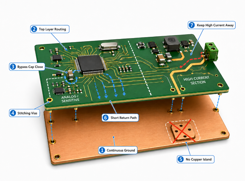
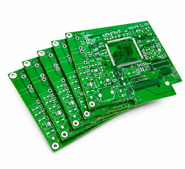
You may also like

What Is Ball Grid Array? BGA Package and PCB Assembly Guide

May 6th, 2026

A Ball Grid Array is a surface-mount IC package that uses solder balls on the underside of the component to connect the chip to a printed circuit board. In modern electronics, BGA packaging is widely used because it supports high pin density, compact PCB layouts, better electrical performance, and improved thermal transfer for advanced components such as CPUs, FPGAs, memory chips, and communication ICs.

This guide explains what a Ball Grid Array is, how BGA solder joints are formed, the common types of BGA packages, assembly and inspection challenges, BGA vs. QFP differences, rework methods, and practical PCB design guidelines for reliable BGA routing.

At EBest Circuit (Best Technology), we support customers with PCB fabrication, component sourcing, SMT assembly, BGA soldering, X-ray inspection, functional testing, and engineering DFM review. With experience in high-density PCB and PCBA manufacturing, our team helps engineers identify layout risks, surface finish issues, via-in-pad requirements, soldering concerns, and inspection needs before production starts. This is especially valuable for projects using BGA CPUs, FPGAs, memory devices, industrial controllers, medical electronics, automotive modules, and communication boards. For BGA PCB assembly support or a project review, pls feel free to contact us at sales@bestpcbs.com.

What Is Ball Grid Array?

What Is a Ball Grid Array?

A Ball Grid Array, often shortened to BGA, is a surface-mount IC package that uses a grid of solder balls on the bottom side of the component to create electrical and mechanical connections with a printed circuit board.

Instead of using visible leads around the package edge, as seen in QFP or SOP packages, a BGA uses the underside of the chip package. Each solder ball connects to a matching pad on the PCB. During reflow soldering, these solder balls melt, wet the PCB pads, and form solid joints after cooling.

This structure allows a compact component to carry a high number of I/O connections. That is why BGA packaging is widely used in processors, memory devices, FPGAs, communication chips, graphics processors, automotive controllers, and high-performance industrial electronics.

A simple way to understand it is this:

Package TypeConnection StyleTypical Use
QFPLeads around the component edgesMedium pin-count ICs
SOPGull-wing leads on two sidesSimple ICs and analog parts
BGASolder balls under the packageHigh-density and high-speed ICs

For modern electronics, BGA is no longer a special package. It is common in compact, fast, and high-reliability PCB assemblies.

What Is Ball Grid Array?

How Does a Ball Grid Array Work on a PCB?

A BGA package works by connecting the IC to the PCB through solder balls arranged in rows and columns. These balls are placed under the package body. The PCB has matching copper pads, usually finished with ENIG, OSP, immersion silver, or another solderable surface finish.

During assembly, solder paste is printed on the PCB pads by stencil. The BGA component is placed on top of the paste. Then the board passes through a reflow oven.

Inside the oven, the temperature gradually rises. The solder paste activates, the solder balls soften and melt, and the component settles into position through surface tension. After cooling, each solder ball becomes a finished solder joint.

This self-centering behavior is one reason BGA assembly can be stable, even with fine pitch parts. However, the process still depends on accurate stencil design, controlled placement, suitable thermal profiling, and proper inspection.

What Are the Advantages of Ball Grid Array Pack IC?

BGA packages became popular because they solve several problems found in traditional leaded IC packages. They support more connections, better speed, and improved thermal paths in a smaller footprint.

High interconnect density

A BGA uses the entire underside of the package, not only the component edges. This gives engineers more connection points within the same area. A large BGA CPU, FPGA, or processor can have hundreds or even thousands of solder balls.

This is especially useful for advanced circuits where many power, ground, and signal pins must be routed in a compact layout.

Better electrical performance

The solder balls create short connection paths between the IC and PCB. Shorter paths usually mean lower inductance and better signal behavior. This matters in high-speed digital circuits, RF modules, memory interfaces, and communication hardware.

For fast signals, package geometry affects impedance, delay, and noise. BGA packaging helps designers achieve a cleaner connection path than long external leads.

Improved thermal transfer

Many BGA packages offer a better path for heat to move from the chip into the PCB. In some designs, thermal balls, copper planes, and via structures can help move heat away from the device.

This is important for BGA CPU packages, power management ICs, network processors, and other components that generate significant heat during operation.

Smaller footprint

Because connections are placed under the component, the package can be more compact than a leaded package with the same pin count. This is valuable in wearable devices, handheld electronics, automotive control modules, telecom modules, and densely populated PCBA designs.

Good assembly stability

During reflow, molten solder tends to pull the BGA into alignment when the placement offset is within process tolerance. This self-alignment effect helps improve placement results. It does not replace process control, but it gives BGA components a practical advantage in automated SMT assembly.

What Are Common Types of BGA Packaging?

Different BGA packages are designed for different electrical, thermal, mechanical, and cost requirements. The best option depends on the application, operating environment, board density, and reliability target.

BGA TypeFull NameMain FeatureCommon Applications
PBGAPlastic Ball Grid ArrayCost-effective organic substrateConsumer electronics, industrial boards
CBGACeramic Ball Grid ArrayHigh thermal and dimensional stabilityAerospace, defense, high-reliability systems
FBGAFine-Pitch Ball Grid ArraySmall pitch and compact sizeMobile devices, memory, compact modules
TBGATape Ball Grid ArrayThin package with flexible tape substrateThin electronics and special designs
FCBGAFlip-Chip Ball Grid ArrayFlip-chip die connection for performanceCPUs, GPUs, ASICs, high-speed processors
WLCSPWafer-Level Chip Scale PackageExtremely small package close to die sizeSmartphones, sensors, compact electronics

PBGA

PBGA is one of the most common types. It uses a plastic body and an organic laminate substrate. It offers a good balance between cost, availability, and performance. Many microcontrollers, ASICs, communication chips, and general ICs use this package.

CBGA

CBGA uses a ceramic substrate. It has excellent thermal stability and is suitable for demanding environments. Ceramic packages are often selected for aerospace, military, high-temperature, or long-life applications.

FBGA

FBGA has a smaller ball pitch and compact body size. It is often used for memory chips, mobile electronics, and miniaturized products. Because the pitch is smaller, PCB routing and assembly control become more demanding.

FCBGA

FCBGA is used in high-performance chips such as CPUs, GPUs, and advanced processors. The die is flipped and connected directly to the package substrate. This improves electrical and thermal performance, making it suitable for high-speed computing applications.

What Is the BGA Solder Reflow Process?

The BGA solder reflow process is the controlled heating cycle that forms solder joints between the BGA package and the PCB. A reliable result depends on correct paste printing, accurate placement, suitable reflow profile, and post-reflow inspection.

The typical process includes these steps:

1. PCB pad preparation

The PCB pads must be clean, flat, and solderable. Surface finish matters. ENIG is often used for fine-pitch BGA because it provides a flat soldering surface. OSP can also be used, but storage and handling control are important.

2. Solder paste printing

Solder paste is printed onto the PCB pads through a stainless steel stencil. Aperture design, stencil thickness, paste type, and printing pressure all affect paste volume.

Too much paste may cause bridging. Too little paste may cause open joints or weak joints.

3. BGA placement

The pick-and-place machine positions the BGA component onto the printed pads. Since the solder balls are hidden under the package, machine accuracy and package recognition are important.

4. Reflow soldering

The PCB enters the reflow oven. A typical lead-free profile includes preheating, soaking, reflow, and cooling. The exact peak temperature depends on the solder alloy, component rating, board thickness, thermal mass, and manufacturer recommendations.

For many SAC lead-free processes, the peak temperature often falls around 235–250°C. For tin-lead soldering, the temperature is lower. The final profile should always follow the component datasheet and assembly process window.

5. Cooling and solidification

After peak temperature, the solder joints cool and solidify. Controlled cooling helps create stable joint structure and reduce thermal stress.

6. Inspection

Because BGA joints are hidden under the component body, visual inspection is not enough. X-ray inspection is commonly used to check solder joint quality, alignment, voids, bridging, and missing connections.

Why Is Ball Grid Array Inspection More Difficult Than Other SMT Packages?

BGA inspection is more difficult because the solder joints are hidden under the package. With QFP, SOP, or other leaded packages, an operator can inspect leads with optical tools. With BGA, the solder joints are not visible from the outside.

This creates several quality control challenges.

Hidden solder joints

A good-looking component body does not prove that the solder joints underneath are good. A BGA may appear correctly placed while still having opens, shorts, voids, or insufficient solder joints.

Void detection

Voids are air pockets inside solder joints. A small amount of voiding may be acceptable depending on the standard and application, but excessive voiding can reduce thermal and mechanical reliability.

Head-in-pillow defects

Head-in-pillow occurs when the solder ball and solder paste touch but fail to fully merge. This defect can pass basic electrical testing at first and later fail under stress or vibration.

Bridging

Bridging happens when solder connects two adjacent balls. This can create short circuits. Fine-pitch BGAs are more sensitive to this issue.

Open joints

An open joint may occur due to insufficient paste, warpage, poor wetting, contamination, or incorrect thermal profile.

Because of these risks, quality-focused PCBA manufacturers use X-ray inspection for BGA solder joints. For critical products, additional testing such as functional testing, thermal cycling, dye-and-pry analysis, or cross-section analysis may be used.

What Are Common BGA Assembly Defects?

BGA assembly can be reliable when the process is controlled. Most defects come from solder paste variation, component warpage, PCB design issues, moisture sensitivity, or thermal imbalance.

DefectWhat It MeansCommon Cause
Open jointOne or more balls fail to connectInsufficient paste, warpage, poor wetting
Solder bridgeAdjacent balls are connected by solderExcess paste, poor stencil design, placement offset
VoidAir pocket inside the solder jointFlux outgassing, paste issue, thermal profile
Head-in-pillowBall and paste do not fully mergeWarpage, oxidation, poor reflow profile
Non-wet openSolder does not wet the pad or ballOxidation, contamination, poor surface finish
Missing ballA solder ball is absent or damagedComponent handling or package defect
Cracked jointJoint cracks after stressCTE mismatch, vibration, thermal cycling

For high-reliability assemblies, BGA quality should be planned before production. The PCB stackup, pad design, stencil design, reflow profile, handling, moisture control, and inspection method all work together.

BGA vs. QFP: Which PCB Packaging Is Right for Your Project?

BGA and QFP packages are both used for IC assembly, but they suit different design requirements. The right choice depends on pin count, routing density, inspection preference, repair needs, and electrical performance.

Comparison ItemBGAQFP
Connection styleSolder balls under packageLeads around package edges
Pin densityHighMedium
Footprint efficiencyExcellentLarger for high pin count
Electrical performanceBetter for high-speed signalsGood for moderate-speed circuits
InspectionRequires X-ray for solder jointsEasier visual inspection
Rework difficultyHigherLower
Routing complexityHigher, especially fine pitchEasier for low to medium pin count
Typical applicationsCPUs, FPGAs, memory, processorsMCUs, interface ICs, control circuits

Choose BGA when your design needs high I/O count, compact size, high-speed performance, or better thermal handling.

Choose QFP when easier inspection, simpler routing, and lower rework complexity are more important than density.

In many real projects, the decision is not purely about cost. It is about the balance between performance, reliability, production capability, and long-term serviceability.

How Are BGA Components Repaired or Reworked?

BGA repair requires specialized equipment because the solder joints are hidden underneath the component. The process is more complex than replacing a leaded IC.

A standard BGA rework process usually includes:

1. Localized heating

A BGA rework station heats the target area with controlled top and bottom heating. This prevents excessive thermal shock and protects nearby components.

2. Component removal

Once the solder joints melt, the defective BGA chip is lifted from the PCB. The operator must avoid pad damage during removal.

3. Pad cleaning

Old solder is removed from the PCB pads. The surface must be flat, clean, and ready for new soldering.

4. Reballing or replacement

If the original component will be reused, it may need reballing. Reballing means placing new solder balls on the package. In many production repair cases, using a new component is safer.

5. Flux application and placement

Flux is applied, and the BGA is aligned on the PCB pads. Accurate positioning is essential.

6. Reflow

The repaired area is heated under a controlled thermal profile. The solder balls melt and form new joints.

7. X-ray and functional testing

After rework, X-ray inspection confirms joint quality. Functional testing confirms electrical performance.

BGA rework should be handled by trained technicians. Excessive heat, poor alignment, or repeated rework can damage the PCB, pads, solder mask, laminate, or nearby components.

What Is BGA Reballing?

BGA reballing is the process of replacing the solder balls on the underside of a BGA component. It is often used when a BGA chip is removed from a PCB and needs to be installed again.

The process usually uses a reballing stencil, solder balls, flux, and controlled heating. The old solder is cleaned from the package pads. New solder balls are aligned and attached to the component.

Reballing may be used in repair work, prototype debugging, chip recovery, or special maintenance projects. However, for high-reliability production, replacing the component with a new part is often preferred.

Reballing quality depends on ball size, pitch accuracy, flux control, surface cleanliness, and heating uniformity.

What Are the Main Design Guidelines for BGA Routing on Multi-layer PCBs?

BGA routing is one of the most important parts of PCB design. A poor fanout strategy can increase layer count, create signal integrity issues, or make fabrication more difficult.

The first step is to review the BGA pitch, ball map, signal groups, power pins, ground pins, high-speed interfaces, and current requirements.

Use the correct land pattern

The pad size should follow the component datasheet and recognized PCB design practices. BGA pads are usually designed as NSMD or SMD pads.

Pad TypeMeaningCommon Use
NSMDCopper pad is smaller than solder mask openingOften preferred for many BGA designs
SMDSolder mask defines the pad edgeUsed in some fine-pitch or special designs

NSMD pads often provide better solder joint shape and copper definition. SMD pads can improve pad anchoring in certain fine-pitch designs. The final choice depends on package pitch, fabricator capability, and reliability needs.

Plan escape routing early

Escape routing means routing signals from inner BGA balls to other areas of the PCB. For coarse-pitch BGAs, dog-bone fanout may be enough. For fine-pitch BGA packages, via-in-pad or microvia technology may be required.

Use via-in-pad carefully

Via-in-pad can save space and support dense routing. However, the via must usually be filled and capped to prevent solder wicking. If solder flows into an open via, the BGA joint may lose solder volume and become unreliable.

Control impedance for high-speed signals

Many BGA components carry DDR, PCIe, USB, Ethernet, RF, or high-speed serial signals. These traces often need controlled impedance, length matching, reference planes, and careful return paths.

Provide strong power and ground planes

BGA CPU packages, FPGAs, and processors often need many power rails. Use proper plane design, decoupling capacitor placement, and low-inductance power delivery paths.

Place decoupling capacitors close to power pins

Decoupling capacitors should be placed close to the relevant BGA power pins. For dense packages, capacitors may be placed on the opposite side of the PCB when layout allows.

Manage thermal performance

For hot BGA devices, add thermal vias, copper planes, and suitable board stackup design. Thermal simulation may be useful for power-dense electronics.

Match PCB fabrication capability

Fine-pitch BGA routing may require HDI PCB technology, laser microvias, small trace/space, filled vias, and precise registration. Before freezing the layout, confirm the PCB supplier’s capability.

How Does BGA Pitch Affect PCB Manufacturing?

BGA pitch refers to the center-to-center distance between adjacent solder balls. A larger pitch is easier to route and assemble. A smaller pitch supports compact designs but increases manufacturing difficulty.

BGA PitchRouting DifficultyTypical PCB Requirement
1.0 mmModerateStandard multilayer PCB often works
0.8 mmModerate to highFine trace/space may be needed
0.65 mmHighHDI may be required
0.5 mmVery highMicrovias and tight process control
0.4 mm or belowAdvancedHDI stackup and experienced assembly process

Fine-pitch BGA designs should be reviewed before PCB fabrication. A DFM review can help check pad size, solder mask clearance, via design, escape routing, stencil aperture, and assembly risk.

What Surface Finish Is Suitable for BGA Assembly?

Surface finish affects solderability, pad flatness, shelf life, and assembly quality. For BGA components, flatness is especially important because the solder balls must sit evenly on the PCB pads.

Surface FinishSuitability for BGANotes
ENIGVery commonFlat surface and good solderability
ENEPIGExcellent for demanding applicationsGood for wire bonding and high reliability
OSPCommon and cost-effectiveRequires good storage and handling
Immersion SilverGood solderabilitySensitive to handling and storage
HASLLess preferred for fine-pitch BGASurface may be less flat

ENIG is widely used for BGA assembly because it provides a flat and stable soldering surface. For high-reliability electronics, ENEPIG may be selected when the application requires stronger finish performance.

Why Is Moisture Sensitivity Important for BGA Components?

Many BGA components are moisture-sensitive. If moisture enters the package and the component is heated too quickly during reflow, internal pressure can build up. This may cause package cracking, delamination, or the well-known “popcorn” effect.

To reduce this risk, assembly teams should follow the component’s moisture sensitivity level, also called MSL. This includes dry storage, controlled floor life, baking when required, and proper handling after opening moisture barrier bags.

Moisture control is especially important for expensive BGA CPU packages, FPGAs, memory devices, and automotive-grade ICs.

How to Choose a Reliable PCB Assembly Partner for BGA Components?

BGA assembly is not only about placing a component on a board. It requires process discipline from PCB fabrication to final inspection.

When choosing a PCBA partner for BGA projects, check whether the supplier can support:

  • Fine-pitch SMT placement
  • Controlled stencil design
  • BGA reflow profile development
  • X-ray inspection
  • BGA rework capability
  • HDI PCB fabrication support
  • Via-in-pad and filled via process
  • Impedance-controlled PCB stackups
  • Component moisture control
  • Functional testing and traceability

For complex BGA boards, engineering support before production is valuable. A good supplier should review pad design, surface finish, stackup, routing density, test access, and assembly risk before mass production.

EBest Circuit supports PCB fabrication, component sourcing, PCB assembly, X-ray inspection, functional testing, and engineering DFM review for BGA and other high-density SMT assemblies. For projects involving BGA CPU, FPGA, memory, RF modules, or industrial control boards, early design review helps reduce risk before the first build.

What Is Ball Grid Array?

In closing, a ball grid array is one of the most important IC package styles in modern electronics. It allows high pin count, compact layout, better electrical performance, and improved thermal paths. These benefits make BGA packaging suitable for CPUs, FPGAs, memory chips, communication ICs, and many other advanced components.

At the same time, BGA assembly requires careful PCB design and strong manufacturing control. The solder joints are hidden, the routing can be dense, and inspection depends heavily on X-ray equipment. For reliable results, engineers should plan the land pattern, fanout, via strategy, surface finish, reflow profile, and inspection method before production.

When BGA design and assembly are handled correctly, it becomes a powerful solution for building smaller, faster, and more reliable electronic products. For BGA PCB assembly, X-ray inspection, or engineering DFM review support, pls feel free to contact EBest Circuit (Best Technology) at sales@bestpcbs.com.

FAQs About Ball Grid Array

What is ball grid array in simple words?

A ball grid array is an IC package that uses solder balls on the bottom side to connect the chip to a PCB. These balls form electrical and mechanical connections during reflow soldering.

What does BGA stand for?

BGA stands for Ball Grid Array. It describes the grid-like arrangement of solder balls under the component package.

What is BGA solder?

BGA solder refers to the solder balls under a BGA package and the solder joints formed between those balls and the PCB pads. In production, solder paste is usually printed on the PCB before reflow.

Why is BGA used for CPUs?

A BGA CPU needs many power, ground, and signal connections in a compact area. BGA packaging supports high pin count, good electrical behavior, and improved thermal transfer, which makes it suitable for processors.

Can BGA components be inspected visually?

Only the outside of the package can be visually inspected. The solder joints are hidden underneath, so X-ray inspection is commonly required for BGA solder joint verification.

Can a BGA chip be repaired?

Yes. A BGA chip can be removed, replaced, or reballed with proper rework equipment. The process requires controlled heating, accurate alignment, pad cleaning, and X-ray inspection after repair.

Is BGA better than QFP?

BGA is better for high-density, high-speed, and compact designs. QFP is easier to inspect and rework. The better choice depends on the project’s electrical, mechanical, cost, and service requirements.

Does BGA require HDI PCB?

Not always. Large-pitch BGA packages may work on standard multilayer PCBs. Fine-pitch BGA components often require HDI technology, microvias, via-in-pad, or tighter trace and space capability.

What causes BGA solder joint failure?

Common causes include poor reflow profile, PCB or package warpage, insufficient solder paste, contamination, excessive voiding, thermal cycling, vibration, and poor pad design.

What is the best PCB surface finish for BGA?

ENIG is commonly used because it provides a flat solderable surface. ENEPIG is also used for demanding applications. OSP can work well when storage and handling are controlled.

You may also like

Medical PCBs Manufacturer | ISO 13485 Assembly

May 5th, 2026

Medical PCBs manufacturer refers to a specialized category of PCB and PCBA production facility that designs, fabricates, and assembles printed circuit boards specifically for use in medical devices and healthcare equipment. This article covers everything engineers and procurement teams need to know — from understanding what a medical PCB is and what materials go into it, to navigating certification requirements and selecting the right manufacturing partner.

Are your medical PCB projects being held back by supplier limitations?

Here are five pain points engineers commonly face when sourcing from a medical PCBs manufacturer:

  • Suppliers lack ISO 13485 or FDA-compliant quality systems, forcing costly re-qualification mid-project.
  • Inconsistent material traceability makes it impossible to meet regulatory audit requirements for PCB for medical devices.
  • Poor DFM feedback results in repeated design revisions that push product launch timelines back by weeks.
  • Minimum order quantities are too high for prototype and clinical trial stages, locking up budget unnecessarily.
  • Limited experience with high-reliability medical PCB design requirements leads to field failures in life-critical applications.

As a professional PCBA manufacturer specializing in medical-grade production, we address these challenges directly:

  • Full ISO 13485 certification and documented quality management processes aligned with medical device regulatory standards.
  • End-to-end material traceability with batch records retrievable within 5 seconds via our digital manufacturing system.
  • 20-year experienced engineers provide DFM analysis and process adaptation advice before fabrication begins.
  • Prototype and small-batch support — no excessive MOQ requirements, enabling fast R&D iteration at clinical trial scale.
  • Dedicated high reliability medical PCB assembly lines with process controls matched to IPC Class 3 standards.

EBest Circuit (Best Technology) is a one-stop PCB and PCBA manufacturer with over 20 years of industry experience, holding ISO 9001/13485, IATF 16949, and AS9100D certifications. Our in-house factory, backed by 1,000+ supply chain partners, serves 1,800+ clients and 10,000+ engineers worldwide — from early-stage prototypes to full production runs. With a digital workshop enabling real-time production tracking and 1.5-week PCBA fast delivery, we bring medical-grade quality and speed together under one roof. For inquiries, pls feel free to contact us at sales@bestpcbs.com.

 Medical PCBs Manufacturer

What Is A Medical PCB?

A medical PCB is a printed circuit board engineered to meet the elevated reliability, biocompatibility, and regulatory traceability standards demanded by the healthcare industry. Unlike commercial or industrial PCBs, medical grade PCB designs must perform without failure in environments where a malfunction can directly harm a patient — making every material choice, soldering parameter, and quality inspection step a matter of life safety.

Medical PCBs appear in an extraordinarily wide range of equipment: from implantable cardiac monitors and surgical robots to portable diagnostic devices and hospital imaging systems. What unites them is a shared manufacturing philosophy — zero tolerance for defects, full traceability of every component and process step, and verified compliance with international medical device standards.

From a technical standpoint, medical PCB design requirements differ from standard PCBs in several measurable ways:

ParameterStandard PCBMedical Grade PCB
IPC Acceptability ClassClass 1 or 2Class 2 or 3 (life support: Class 3)
Cleanliness StandardIPC-CH-65 basicIPC-CH-65 strict; ionic contamination tested
Component TraceabilityBatch-levelFull lot-level, lot-date code recorded
Solder Quality InspectionAXI or visualAXI + AOI + cross-section verification
Reliability TestingStandard burn-inExtended HALT/HASS, thermal cycling
DocumentationStandard BOMFull DHR (Device History Record) per FDA 21 CFR Part 820

Understanding what sets a medical PCB apart is the foundation for making every downstream decision — material selection, manufacturer qualification, and regulatory submission — correctly the first time.

 Medical PCBs Manufacturer

What Are The Types Of Medical PCBs?

Medical PCBs span a wide spectrum of form factors, layer counts, and substrate materials, each matched to a specific class of medical device application. Choosing the right board type is a critical early design decision that affects both performance and manufacturing cost.

The main types used in medical device PCBs manufacturing are:

1. Rigid PCBs The most common type in medical applications. Multi-layer rigid boards (typically 4–12 layers) are used in diagnostic imaging equipment, patient monitors, laboratory analyzers, and hospital network infrastructure. They offer dimensional stability, high circuit density, and mature manufacturing processes suited to IPC Class 3 assembly.

2. Flexible PCBs (Flex PCBs) Used wherever the circuit must bend, fold, or conform to a curved surface — wearable biosensors, endoscope camera assemblies, hearing aids, and implantable devices. Flex PCBs reduce connector count (a major reliability risk point), decrease assembly weight, and enable compact form factors impossible with rigid boards.

3. Rigid-Flex PCBs A hybrid construction combining rigid sections (for component mounting) with flexible sections (for dynamic interconnect). Rigid-flex is widely used in implantable devices, surgical tools, and portable diagnostic equipment where both mechanical robustness and spatial efficiency are required.

4. High-Density Interconnect (HDI) PCBs HDI technology — featuring microvias, blind vias, and buried vias — enables extremely fine trace widths (down to 3 mil / 75 µm) and component pitches. Essential for modern wearable medical devices, portable ultrasound units, and miniaturized implantables where every square millimeter of board space is constrained.

5. Metal Core PCBs (MCPCBs) For applications generating significant heat — LED surgical lighting, power supply units in imaging equipment, and high-current motor driver boards in surgical robots — metal core (typically aluminum) substrates provide thermal conductivity of 1–3 W/(m·K), compared to standard FR-4 at 0.3 W/(m·K).

6. Ceramic PCBs Alumina (Al₂O₃) and aluminum nitride (AlN) ceramic substrates offer superior thermal conductivity (up to 170 W/(m·K) for AlN), excellent biocompatibility, and outstanding chemical resistance. Used in implantable neurostimulators, cochlear implant electronics, and high-frequency RF medical devices.

The board type selection should always begin with the device’s operating environment — temperature range, mechanical stress, size envelope, and regulatory class — before moving to layer count and material specification.

What Are The Key Requirements For Medical PCB Manufacturing?

Medical PCB manufacturing is governed by a set of technical and regulatory requirements that go significantly beyond what is expected in consumer or industrial PCB production. Meeting these requirements is not optional — they are the baseline for any product destined for regulatory submission.

Reliability and Quality Standards

Medical devices are categorized by risk level, and the PCB manufacturing standard follows accordingly:

Device Risk ClassExample DevicesIPC Assembly ClassRequired Reliability Level
Class I (Low Risk)Bandages, tongue depressors with electronicsIPC Class 2Standard
Class II (Moderate Risk)Patient monitors, infusion pumps, diagnostic equipmentIPC Class 2–3High
Class III (High Risk)Implantable pacemakers, defibrillators, neurostimulatorsIPC Class 3Ultra-high

Core manufacturing requirements include:

  • Controlled processes: Every soldering profile, cleaning cycle, and inspection step must be documented, validated, and repeatable. Process deviations must trigger corrective action (CAPA) records.
  • IPC Class 3 workmanship: For life-critical devices, solder joints, via fills, and copper plating thickness are held to IPC-A-610 Class 3 acceptance criteria — zero tolerance for lifted pads, cold joints, or incomplete hole fill.
  • Ionic contamination control: Post-reflow cleaning must bring residual ionic contamination below 1.56 µg/cm² NaCl equivalent (per IPC-CH-65), verified by ROSE or SIR testing.
  • Electrostatic Discharge (ESD) protection: Medical PCB assembly areas must maintain ESD-safe environments (< 100 V) per ANSI/ESD S20.20, as many sensitive medical ICs have ESD withstand voltages below 500 V.
  • Full material traceability: Every component lot, bare board batch, and solder paste date code must be recorded in a Device History Record (DHR) that can be retrieved and submitted during FDA or CE audits.
  • Change control: Any change to materials, processes, or suppliers must follow a formal change notification (PCN) process, with re-validation data before the change takes effect.

These requirements define the minimum bar any medical PCBs manufacturer must meet — not just during certification audits, but on every production lot, every day.

What Certifications Should A Medical PCBs Manufacturer Have?

Certification is the most objective way to evaluate whether a medical PCBs manufacturer operates a quality system genuinely capable of supporting regulatory submissions. The right certifications are not marketing badges — they represent audited, third-party-verified evidence of process discipline.

The essential certifications to require:

ISO 13485 — Medical Device Quality Management System This is the non-negotiable baseline. ISO 13485 is the international standard specifically designed for organizations involved in the design and manufacture of medical devices and their components. It requires documented procedures for risk management, design control, process validation, complaint handling, and CAPA. A PCB manufacturer without ISO 13485 cannot be qualified as a direct supplier for any Class II or Class III medical device.

FDA 21 CFR Part 820 — Quality System Regulation (USA) For devices sold in the US market, the manufacturing facility must comply with FDA’s Quality System Regulation. Key requirements include design controls, corrective and preventive action (CAPA) systems, and complete Device History Records (DHRs). A manufacturer supplying FDA-registered device makers is expected to be audit-ready at all times.

IPC-A-610 Class 3 Certification IPC-A-610 is the global acceptability standard for electronic assemblies. Class 3 certification means the manufacturer’s inspection operators are trained and certified to apply the most stringent acceptance criteria — the standard for high-reliability and life-support equipment.

ISO 9001 — General Quality Management System The foundational QMS standard. Most medical PCB manufacturers hold both ISO 9001 and ISO 13485; ISO 9001 alone is insufficient for medical device applications.

Additional certifications that add confidence:

CertificationRelevance to Medical PCB
IATF 16949Process discipline from automotive; indicates process control maturity
AS9100DAerospace-grade quality systems; relevant for high-reliability implantables
UL CertificationSafety approval for specific board materials and constructions
RoHS ComplianceRequired for CE-marked medical devices sold in the EU
REACH ComplianceChemical substance compliance for EU market access

When evaluating a biomedical PCB manufacturing partner, always request current, valid certificates — not expired documents — and verify that the scope of certification explicitly covers PCB and PCBA manufacturing, not just the company’s headquarters or administrative functions.

What Materials Are Used In Medical Device PCBs Manufacturing?

Material selection in medical device PCBs manufacturing directly determines electrical performance, thermal management, biocompatibility, and long-term reliability. Unlike commercial PCB designs where cost optimization is the primary driver, medical PCB material choices are governed first by performance and regulatory compliance, then by cost.

Substrate Materials:

MaterialThermal ConductivityKey PropertiesTypical Medical Application
FR-4 (High-Tg)0.3 W/(m·K)Stable up to 170°C Tg; cost-effectivePatient monitors, diagnostic equipment
Polyimide0.2 W/(m·K)Flexible, wide temp range (−65°C to +260°C)Flex PCBs, wearable biosensors, implantables
Alumina (Al₂O₃)20–30 W/(m·K)Biocompatible, chemical resistantImplantable devices, RF medical equipment
Aluminum Nitride (AlN)140–170 W/(m·K)Highest thermal conductivity ceramicHigh-power implantables, laser medical devices
PTFE / Rogers0.2–0.7 W/(m·K)Low Dk/Df for high-frequency signalsWireless medical devices, imaging systems
Aluminum Core (MCPCB)1–3 W/(m·K)Excellent heat dissipationLED surgical lighting, power supply boards

Surface Finish Options:

The surface finish affects solderability, shelf life, and — critically for implantable or skin-contact devices — biocompatibility:

  • ENIG (Electroless Nickel Immersion Gold): The standard choice for medical PCB assembly. Flat, solderable, and nickel barrier prevents copper migration. Shelf life: 12 months.
  • ENEPIG (Electroless Nickel Electroless Palladium Immersion Gold): Preferred for wire bonding applications in implantable sensors. Palladium layer improves gold wire bond adhesion.
  • OSP (Organic Solderability Preservative): Low cost, RoHS-compliant, but short shelf life (6 months). Acceptable for non-implantable disposable medical devices.
  • Hard Gold: Used on edge connectors and contact fingers subject to repeated insertion cycles — common in diagnostic instrument PCB card-edge interfaces.

Solder Alloy:

For medical devices, SAC305 (Sn96.5/Ag3.0/Cu0.5) is the industry standard lead-free alloy. It offers a good balance of mechanical strength, thermal fatigue resistance, and process maturity. For implantable devices requiring even higher joint reliability, some manufacturers specify SAC405 or bismuth-modified alloys for specific joint geometries.

Material selection should always be documented in the design specification and reviewed during DFM analysis to confirm compatibility with the manufacturing process before bare board fabrication begins.

How Are Medical PCBs Manufactured?

Medical PCB manufacturing follows the same fundamental process sequence as standard PCB production, but every step is executed under tighter process controls, with mandatory documentation and inspection gates that would be optional in commercial production.

Here is the end-to-end manufacturing flow for a typical high reliability medical PCB assembly:

Step 1 — Design Review and DFM Analysis Before any material is ordered, the PCB design files (Gerber, ODB++, IPC-2581) and BOM are reviewed against medical PCB design requirements. DFM analysis checks for minimum annular rings, acid traps, copper clearance violations, and test point accessibility. A written DFM report is issued with recommended modifications.

Step 2 — Bare Board Fabrication The PCB substrate is fabricated per the design specification. For medical applications, key in-process controls include:

  • Copper thickness verification (inner layers: ±10% of nominal)
  • Drill registration and hole size (±0.05 mm for Class 3)
  • Impedance control verification (±10% for controlled impedance designs)
  • Electrical testing: 100% net continuity and isolation testing before lamination

Step 3 — Component Sourcing and Incoming Inspection Components are sourced from authorized distributors only — no gray-market or counterfeit-risk channels. Incoming inspection includes:

  • Certificate of Conformance (CoC) verification for every lot
  • Date code and lot code recording in the DHR
  • Visual inspection and functional sampling per AQL level

Step 4 — SMT Assembly Solder paste printing, component placement, and reflow soldering are executed on calibrated SMT lines. Process controls include:

  • Solder paste inspection (SPI) after printing — volume, area, and height verified on every board
  • Pick-and-place accuracy: ±0.05 mm for standard components; ±0.03 mm for fine-pitch ICs
  • Reflow profile validated and recorded per component manufacturer specifications

Step 5 — Post-Reflow Inspection

  • AOI (Automated Optical Inspection): 100% inspection of solder joint geometry, component presence, polarity, and alignment
  • AXI (Automated X-Ray Inspection): Mandatory for BGAs, QFNs, and any bottom-terminated components where solder joints are hidden
  • Cross-section analysis: Performed on sample boards per lot to verify via fill quality and solder joint microstructure

Step 6 — Cleaning and Cleanliness Verification Post-reflow aqueous or semi-aqueous cleaning removes flux residues. Ionic contamination is tested per IPC-CH-65 to confirm residual contamination is below the medical-grade threshold.

Step 7 — Functional and In-Circuit Testing ICT verifies component values, solder joint continuity, and short circuits across all test points. FCT validates the board’s functional performance against the device specification — voltages, currents, signal frequencies, and communication interfaces are all exercised.

Step 8 — Final Inspection and Documentation Each board receives a final visual inspection per IPC-A-610 Class 3 criteria. The completed DHR — including all material lot records, process parameter logs, inspection results, and test data — is archived for regulatory traceability.

This disciplined, gate-driven process is what separates a genuine medical PCBs manufacturer from a general-purpose assembly house that simply claims to handle medical work.

How To Choose A Reliable Medical PCBs Manufacturer?

Selecting the right medical PCBs manufacturer is one of the highest-stakes procurement decisions in medical device development. The wrong choice can result in regulatory delays, product recalls, or — in the worst case — patient harm. The right choice accelerates your path from prototype to market while building a quality record that withstands regulatory scrutiny.

Evaluate candidates against these seven criteria:

1. Certification Scope — Not Just the Certificate Confirm that ISO 13485 certification explicitly covers the PCB fabrication and PCBA assembly operations at the specific facility you will use — not just the company’s headquarters. Request the latest audit report summary and verify there are no open major nonconformances.

2. Medical PCB Experience and References Ask for examples of completed medical device projects — device category (not necessarily the exact device), IPC class, and regulatory market (FDA, CE, PMDA). A manufacturer with 10 years of general PCB experience is very different from one with 10 years of specifically medical device PCBs manufacturing experience.

3. DFM Capability A reliable partner does not just build what you send them — they review it first. The quality of a manufacturer’s DFM feedback (depth of analysis, speed of response, clarity of the report) is a strong predictor of how they will handle process issues during production.

4. Traceability Infrastructure Ask directly: “How do you generate the Device History Record for each production lot, and how quickly can you retrieve it for an FDA audit?” The answer should describe a documented system — not a manual spreadsheet process. Digital manufacturing systems that enable 5-second batch traceability are the benchmark.

5. Test Coverage Confirm that the manufacturer operates ICT, AOI, AXI, and FCT in-house — not outsourced. For IPC Class 3 work, all four test methods are typically required. Ask for specifics on fixture capability (probe pitch, net coverage percentage) and FCT programmability.

6. Prototype and Scale Flexibility Medical device development involves multiple design iterations before a design freeze. A manufacturer that imposes high MOQs or long lead times on prototype orders will slow your development cycle. Look for a partner that supports small-batch and prototype orders with the same quality controls applied to production runs.

7. Communication and Engineering Support Responsiveness matters. A manufacturer that assigns you a dedicated application engineer — someone who understands medical PCB design requirements and can engage technically — is worth significantly more than a low-cost supplier that only communicates through a sales portal.

The best medical PCBs manufacturer is not necessarily the cheapest or the largest — it is the one whose quality system, engineering capability, and process controls are most closely matched to the specific demands of your device and its target regulatory market.

How Can EBest Circuit (Best Technology) Support Your Medical PCB Projects?

Supporting medical PCB projects from first prototype through certified production requires an integrated manufacturing capability that very few suppliers can genuinely offer. EBest Circuit (Best Technology) has built that capability over 20 years, specifically to serve engineers developing complex, high-reliability products — including medical devices.

Our medical PCB support process:

1. Pre-Production DFM and Medical PCB Design Requirements Review Our 20-year experienced PCB/PCBA engineers review your Gerber files, BOM, and design specification before a single panel is fabricated. We issue a written DFM report covering trace clearance, via design, test point accessibility, component spacing, and IPC Class compliance — with a corresponding BOM optimization list that flags long-lead or obsolete medical components before they become a production problem.

2. ISO 13485-Certified Quality Management System Our production operations are certified to ISO 13485, ISO 9001, IATF 16949, and AS9100D. Every medical PCB assembly job runs under a documented quality plan — including incoming inspection records, process parameter logs, inspection results, and a complete Device History Record (DHR) that is audit-ready from day one.

3. Full Material Traceability in 5 Seconds Our digital manufacturing workshop tracks every material lot, component date code, and production batch in real time. Any traceability query — “which lot of solder paste was used on board serial number X?” — is answerable within 5 seconds. This is the traceability infrastructure your regulatory submissions require.

4. IPC Class 3 Assembly and Inspection Our SMT lines are configured for IPC Class 3 medical PCB assembly, with 100% SPI, AOI, and AXI inspection as standard for medical projects. Our FCT stations are programmable to your device test plan, covering voltage rails, signal integrity, communication interfaces, and functional performance verification.

5. Prototype to Production — No Gap in Quality We support prototype quantities (as low as 5 pcs) and small-batch clinical trial builds with the same certified processes applied to full production. There is no “prototype mode” with relaxed controls — every medical board, at every quantity, runs under the same ISO 13485 quality system.

6. 1.5-Week PCBA Fast Delivery Our integrated in-house PCB fabrication and PCBA assembly eliminates inter-supplier hand-off delays. For qualifying medical PCB projects, we deliver completed, tested assemblies in as fast as 1.5 weeks — without compromising on the process controls your device requires.

Whether you are developing a wearable biosensor, a Class II diagnostic instrument, or a high-reliability implantable device, EBest Circuit (Best Technology) has the engineering depth, certified quality infrastructure, and manufacturing capacity to be a long-term partner in your medical device supply chain. If any questions, pls feel free to contact our team anytime at sales@bestpcbs.com.

 Medical PCBs Manufacturer

To sum up, medical PCBs manufacturer is a precise term for a highly specialized category of electronics production partner — one that combines advanced fabrication and assembly capabilities with certified quality management systems, rigorous material traceability, and deep familiarity with the regulatory requirements of the healthcare industry. This article has covered the full landscape: from understanding what a medical PCB is and which types apply to different device categories, to the materials, processes, certifications, and selection criteria that define a genuinely capable manufacturing partner.

Choosing the right medical PCBs manufacturer is not a cost decision — it is a quality and compliance decision that will define your regulatory submission timeline, your field reliability record, and your ability to scale from prototype to production without disruption.

At EBest Circuit (Best Technology), we bring 20 years of certified PCB and PCBA manufacturing expertise to every medical device project. Our ISO 13485-certified quality system, IPC Class 3 assembly capability, 5-second material traceability, and 1.5-week delivery mean your medical PCB project gets the engineering rigor it demands — and the speed your development schedule requires. From the first DFM review to the final DHR, we are built to be the manufacturing partner your medical device deserves.

Ready to start your next medical PCB project? Pls feel free to contact our team anytime at sales@bestpcbs.com.

FAQs About Medical PCBs Manufacturer

Q: What is the difference between a standard PCB manufacturer and a medical PCBs manufacturer?

A: The core difference lies in the quality system, not the equipment. A medical PCBs manufacturer operates under ISO 13485 certification, applies IPC Class 2 or Class 3 assembly standards, maintains full lot-level material traceability, and generates Device History Records (DHRs) for every production lot. Standard PCB manufacturers typically operate under ISO 9001 only, without the medical-specific documentation and process control requirements. For any PCB for medical devices that will be submitted to FDA or CE regulatory review, the manufacturer must meet medical-grade requirements.

Q: Is ISO 13485 certification mandatory for a medical PCBs manufacturer?

A: For direct suppliers to medical device companies — yes, in practice. While ISO 13485 is technically a voluntary standard, most medical device OEMs require it as a contractual supplier qualification condition, and regulatory bodies (FDA, EU MDR) expect manufacturers to demonstrate supplier control through certified QMS documentation. A medical PCBs manufacturer without ISO 13485 will almost certainly fail OEM supplier audits for Class II and Class III device programs.

Q: What IPC class applies to medical PCB assembly?

A: It depends on the device risk class. Class II medical devices (patient monitors, infusion pumps, diagnostic equipment) are typically assembled to IPC Class 2 as a minimum, with many OEMs specifying IPC Class 3 for added reliability assurance. Class III devices (implantable pacemakers, defibrillators, neurostimulators) universally require IPC Class 3, which mandates the most stringent solder joint and workmanship acceptance criteria. Confirm the required IPC class with your device risk classification and OEM specification before engaging any medical PCBs manufacturer.

Q: How do I verify that a medical PCBs manufacturer’s traceability system meets FDA requirements?

A: Request a sample Device History Record (DHR) from a previous production lot — with customer-confidential information redacted. A compliant DHR should contain: the device identification and revision, dates of manufacture, quantity manufactured and released, inspection and test records, component lot codes and date codes, and the names of personnel performing key operations. If the manufacturer cannot produce a complete sample DHR quickly and confidently, their traceability system is unlikely to survive an FDA 21 CFR Part 820 audit.

Q: Can a medical PCBs manufacturer support both prototypes and production volumes?

A: The best partners do. Early-stage medical device development requires frequent design iterations, often in quantities of 5–50 units, before a design freeze is reached. A manufacturer that imposes high MOQs or applies relaxed quality controls on small runs forces engineers to switch suppliers between development and production — which introduces re-qualification risk and delays. Look specifically for a medical PCBs manufacturer that applies the same certified quality system to prototype builds as to production lots, regardless of quantity.

Q: What certifications should I ask for when qualifying a biomedical PCB manufacturing supplier?

A: At minimum, require: ISO 13485 (current, with scope covering PCB/PCBA manufacturing), ISO 9001, and evidence of IPC-A-610 Class 3 operator certification. For devices targeting the US market, confirm familiarity with FDA 21 CFR Part 820 requirements. For EU MDR submissions, confirm RoHS and REACH compliance documentation. For high-reliability or implantable applications, AS9100D certification is an additional indicator of process control maturity. Always request current certificates — not photocopies of expired documents — and verify the certification body is accredited.

You may also like

Circuit Board Test Points | From PCB Fabrication To PCBA Test

May 5th, 2026

Circuit board test points are designated access locations on a Printed Circuit Board (PCB) that enable engineers and technicians to measure electrical signals, verify functionality, and isolate faults throughout the manufacturing and assembly process. This article covers everything you need to know — from understanding what test points are and how to place them, to leveraging them effectively across the full journey from PCB fabrication to PCBA test.

Are your test points costing you time and yield instead of saving them?

Here are five pain points engineers commonly face with circuit board test points:

  • Test point locations conflict with components or heatsinks, making probing physically impossible.
  • Inconsistent probe contact causes floating or inaccurate voltage readings during ICT.
  • High-density SMD layouts leave no room for standard through-hole test points.
  • Automated bed-of-nails fixtures fail due to poor pad geometry or incorrect pitch on SMD test points.
  • Insufficient test coverage on critical nets leads to escaped defects that only surface in the field.

As a professional PCBA manufacturer, we tackle these issues head-on:

  • DFM pre-screening ensures test points on a circuit board are placed in accessible, probe-friendly zones.
  • High-quality pad materials and controlled-impedance design minimize resistance and signal distortion.
  • SMD test point recommendations are tailored to your board density and height constraints.
  • Pad geometry is optimized for compatibility with standard compact probe tip circuit board test points.
  • Full net coverage analysis guarantees all critical signals — power, ground, clocks — have dedicated test points.

EBest Circuit (Best Technology) is a one-stop PCB and PCBA manufacturer with 20+ years of industry experience, serving 1,800+ clients and 10,000+ engineers worldwide. Our in-house factory, 1,000+ supply chain partners, and ISO 9001/13485, IATF 16949, and AS9100D certifications ensure precision from bare board to finished assembly. With a 20-year experienced engineering team offering DFM analysis, BOM optimization, and process adaptation advice, we deliver PCBA in as fast as 1.5 weeks. For inquiries, pls feel free to contact us at sales@bestpcbs.com.

circuit board test points

What Are Circuit Board Test Points?

Circuit board test points are small, exposed metal pads, vias, or mechanical pins placed on a PCB to provide safe, repeatable access for test equipment. Think of them as the “nerve endings” of your board — each one giving a diagnostic window into what is happening electrically at that exact location, without requiring you to probe fragile IC legs or lift solder joints.

From the earliest stage of PCB fabrication through to PCBA functional testing, printed circuit board test points appear in several physical forms:

TypeConstructionTypical Use Case
Solder Pad (SMD)Flat copper pad, no through-holeHigh-density, low-profile boards
Through-Hole ViaPlated hole exposed on both sidesManual probing, dual-sided access
Mechanical Pin (Keystone)Press-fit or soldered pinRepeated manual probing, durability
Testpad on Ground PlaneLarge copper islandReference ground for oscilloscope probes

Each test point circuit board design targets a specific combination of probe compatibility, board density, and test frequency. The golden rule is simple: a test point that cannot be reached by a probe is no test point at all.

Electrically, test points act as low-impedance windows onto signal nets. When correctly designed, they introduce negligible loading — typically less than 1 pF of parasitic capacitance on a well-laid-out SMD pad — preserving signal integrity for measurements on high-speed nets. Poorly designed pads, however, can act as stubs that distort waveforms, especially above 100 MHz.

In short, circuit board test points are the foundation of any robust In-Circuit Test (ICT) or Functional Circuit Test (FCT) strategy, and their quality directly determines how efficiently a board can move from fabrication to verified, shippable product.

circuit board test points

What Are Keystone Test Points In PCB Design?

Keystone test points refer to a family of small, mechanically robust test hardware — most commonly press-fit or soldered pins — originally manufactured by Keystone Electronics and now widely replicated across the industry. Unlike a simple copper pad, a Keystone-style test point is a physical component that stands proud of the board surface, giving a probe tip a clearly defined and durable landing zone.

Keystone test points are typically available in the following configurations:

  • Thru-hole pins: Pressed or soldered into a plated through-hole; extremely robust for high-cycle manual probing environments.
  • Surface-mount loop or pad variants: Low-profile options for boards with height restrictions, retaining mechanical durability while reducing z-axis space.
  • Color-coded versions: Red (positive/signal), black (ground), white (neutral) — essential for quick identification during manual debugging.
  • Miniature SMD versions: For fine-pitch, high-density designs where even a standard 1 mm pad may be too large.

The mechanical advantage of a Keystone-style component over a bare pad becomes especially apparent in manufacturing environments where the same board is probed hundreds or thousands of times during ICT. A bare copper pad can oxidize, deform under repeated contact, or delaminate from the substrate. A properly installed Keystone pin resists all three failure modes.

From a PCB design perspective, integrating these components requires a dedicated footprint with sufficient keep-out clearance so that neighboring components do not obstruct probe access. Most designers allocate a 1.0–1.5 mm clearance radius around each pin, confirmed during DFM review before fabrication begins.

In summary, Keystone test points bridge the gap between a fragile solder pad and a bulky connector — delivering the mechanical reliability of a connector with the PCB footprint of a test pad.

Why Are PCB Test Points Important In Assembly?

PCB test points are the quality gatekeepers of the PCBA process. Without them, a finished board is essentially a black box — you can power it on and observe behavior, but you cannot pinpoint where a fault originates. With them, every critical net becomes observable, and every manufacturing defect becomes traceable.

The impact is measurable across multiple dimensions of production:

AspectWithout Test PointsWith Test Points
Fault IsolationHours of blind signal tracingMinutes with direct probe access
ICT CompatibilityBed-of-nails fixture impossibleFull automated ICT enabled
Signal Integrity RiskHigh — probing IC pins risks damageLow — isolated pad absorbs probe force
First-Pass YieldLower — defects escape to FCT or fieldHigher — shorts and opens caught early
Rework CostHigh — faults found late cost more to fixLow — defects caught at source

During SMT assembly, the most common defect categories — solder bridges, cold joints, missing components, and reversed polarities — are all detectable through properly placed test points on a circuit board. An ICT system using a bed-of-nails fixture can test hundreds of nets in under 10 seconds, but only if each net has a dedicated, accessible test point.

Beyond ICT, PCB test points also support:

  • In-System Programming (ISP): JTAG and SWD test points allow firmware flashing directly on the production line.
  • Boundary Scan Testing: IEEE 1149.1-compliant test point clusters enable digital chain testing of complex ICs.
  • Burn-in Monitoring: Test points on power rails allow continuous voltage and current monitoring during thermal stress testing.

The ROI of good test point design is straightforward: early defect detection at the ICT stage costs a fraction of the rework or warranty cost incurred when a defect escapes to the customer. For high-volume production runs, a 1% improvement in first-pass yield can translate directly into tens of thousands of dollars in savings per quarter.

Where Are The Test Points On A Circuit Board?

Knowing where test points on a circuit board are located — and why — is as important as knowing what they are. Placement is not arbitrary; it follows a set of design principles that balance electrical accessibility, physical reachability, and automated test fixture compatibility.

Primary placement zones include:

  • Board edges and corner areas — Low component density in these zones makes probe access straightforward and reduces fixture complexity.
  • Near power regulators and DC-DC converters — Voltage rails must be verified at the output of every regulation stage.
  • Adjacent to microcontrollers and FPGAs — Clock lines, reset signals, and communication buses (I²C, SPI, UART) all benefit from dedicated test points.
  • On crystal oscillator outputs — Frequency verification requires a clean, low-capacitance measurement point close to the source.
  • On all power and ground nets — A solid ground reference test point within 20 mm of every signal test point is best practice for oscilloscope probing.
  • On high-current traces — Current-sense resistor terminals with dedicated test points allow in-circuit current measurement without breaking the circuit.

Placement rules to follow:

  • Never position a test point underneath a heatsink, shield can, or tall electrolytic capacitor.
  • Maintain a minimum of 1.0 mm clearance between adjacent test points on ICT fixtures to prevent probe cross-contact.
  • For double-sided ICT, mirror critical test points on both top and bottom layers to allow a two-sided fixture.
  • Keep test point pitch ≥ 2.54 mm (100 mil) for standard bed-of-nails probes; for fine-pitch ICT, 1.27 mm (50 mil) is achievable with precision fixtures.

During DFM analysis, our engineers review Gerber files specifically to confirm that all test points on circuit board layouts are reachable, correctly sized, and free of solder mask obstruction. An exposed, soldermask-free copper pad is the baseline requirement — any mask coverage over a test point renders it unreliable.

How To Use Test Points On A Circuit Board?

Understanding how to use test points on a circuit board correctly is essential for obtaining reliable measurements and avoiding board damage. The process is straightforward, but each step matters.

Step-by-step guide to probing test points:

  • Identify the test point using the schematic or PCB layout file. Cross-reference the reference designator (e.g., TP1, TP_GND) with the net it monitors. Do not guess — probing the wrong net can give misleading data or cause a short.
  • Select the right probe tip. For SMD pads smaller than 1 mm, use a fine-tipped probe (0.5 mm diameter or less). For through-hole or Keystone pins, a standard 1 mm hook probe works well. Compact probe tip circuit board test points require matched probe geometry for consistent contact.
  • Set up your instrument correctly. To measure ar test points on a circuit board for volts, confirm whether the net is DC or AC, then set your multimeter or oscilloscope to the appropriate range and coupling. For power rails, DC voltage mode is standard. For clock or data lines, use AC coupling with the correct oscilloscope bandwidth.
  • Make contact gently but firmly. Place the probe perpendicular to the pad surface. Avoid dragging the tip across the board, which can dislodge nearby 0201 or 0402 components. For oscilloscope measurements, always connect the ground clip to the nearest ground test point — not to a remote chassis ground — to minimize loop inductance.
  • Read and record the measurement. Compare against the expected value from the design specification. Flag any deviation exceeding ±5% on power rails or unexpected waveform distortion on signal nets.
  • Do not apply excessive force. SMD test pads are bonded to the PCB substrate through copper traces and soldermask. Repeated heavy probing can delaminate the pad, especially on thin (0.8 mm) boards.

Quick reference for common measurements:

MeasurementInstrumentModeReference Point
DC power rail voltageMultimeterDC VoltageGND test point
Clock frequencyOscilloscopeAC, 10× probeNearest GND
I²C signal integrityOscilloscopeAC, 1× probeGND test point
In-circuit resistanceMultimeterResistance (power OFF)N/A

Following this process consistently makes test points on a circuit board a genuinely powerful diagnostic tool rather than a source of measurement error.

When Should You Use An SMD Test Point?

An SMD test point is the default choice for the vast majority of modern PCB designs. As board complexity has increased and component pitch has shrunk, through-hole test points have become the exception rather than the rule. Understanding when to specify an SMD test point — and which variant to choose — directly affects your testability, board density, and manufacturing cost.

Use an SMD test point when:

  • The board uses double-sided SMT assembly. Through-hole pins require wave soldering or hand soldering, which adds process steps. SMD variants are reflowed with the rest of the components.
  • Height clearance is restricted. In flat consumer electronics or wearables, even a 1 mm tall Keystone pin may exceed the allowable z-axis envelope. An SMD pad adds zero height.
  • The board density is high. On a 6-layer or 8-layer HDI board with 0201 passives, the footprint of a through-hole test point competes directly with signal routing. An SMD pad (typically 0.8 mm × 1.2 mm) integrates without displacing any traces.
  • Automated ICT is planned. Bed-of-nails fixtures are designed around consistent SMD pad locations, which are photolithographically defined and highly repeatable in position.
  • The test point will be probed infrequently. For production-line ICT, SMD pads survive thousands of probe contacts with minimal wear. For daily manual probing in a lab setting, a Keystone pin offers better longevity.

SMD test point pad sizing guidelines:

Board Pitch EnvironmentRecommended Pad DiameterSolder Mask Opening
Standard (≥ 0.5 mm pitch)1.0 mm1.2 mm
Fine-pitch (0.3–0.5 mm)0.7 mm0.9 mm
Ultra-fine / HDI0.5 mm0.65 mm

One important design note: SMD test points should always be placed on the solder mask layer with an explicit opening (NSMD — non-solder mask defined) to ensure the copper pad is fully exposed and oxidation-free when the board arrives at the ICT station. A test point buried under solder mask is electrically invisible to a probe.

How Do Probe Tip Circuit Board Test Points Improve Testing?

The physical interface between a probe tip and a PCB test point is where theory meets reality. Even a perfectly designed test point becomes unreliable if the probe tip is mismatched in geometry, spring force, or material. Probe tip circuit board test points — the combined system of pad and probe — must be engineered together, not independently.

Why probe-pad compatibility matters:

A standard ICT bed-of-nails probe tip exerts between 50 g and 150 g of force on each test point. If the pad diameter is smaller than the probe tip contact area, the probe can slip, bridge to an adjacent trace, or fail to make reliable ohmic contact. The result is false failures on a good board — one of the most expensive problems in PCBA production, because it drives unnecessary rework.

Key parameters of the probe-pad interface:

ParameterEffect on Test Reliability
Probe tip diameter vs. pad diameterMust be ≤ pad diameter; mismatch causes slippage
Spring forceToo low → intermittent contact; too high → pad delamination
Tip material (beryllium copper vs. tungsten)Tungsten for hard surfaces; BeCu for gold-plated pads
Contact resistanceTarget < 10 mΩ; higher values introduce voltage offset errors
Probe pitchMinimum 2.54 mm for standard fixtures; 1.27 mm for fine-pitch

Compact probe tip circuit board test points — a combination of miniaturized pads (≤ 0.8 mm) paired with precision fine-tipped probes — are used specifically in high-density designs where standard fixtures cannot achieve the required test coverage. These systems are more expensive but essential for complex boards where testability cannot be sacrificed for density.

Benefits across the production lifecycle:

  • ICT stage: Consistent probe contact yields repeatable resistance and capacitance measurements, enabling accurate solder joint quality verification.
  • FCT stage: Oscilloscope probes with fine tips can access high-speed signal test points (e.g., USB 3.0, MIPI) without adding the capacitive loading of a large hook probe.
  • Field debugging: A well-designed probe tip and pad system allows field service engineers to diagnose board failures in-system without removing the PCB from the enclosure.

The takeaway is clear: specifying probe tip circuit board test points as a matched system — not as separate pad and probe decisions — is what separates a testable, manufacturable design from one that struggles at every quality gate.

How Can EBest Circuit (Best Technology) Support Circuit Board Test Points From PCB Fabrication To PCBA Test?

Supporting circuit board test points throughout the full production lifecycle — from the first Gerber review to the final functional test — requires more than equipment. It requires process integration, engineering expertise, and quality infrastructure that spans every stage. EBest Circuit (Best Technology) provides exactly that.

Our end-to-end support process:

1. DFM Analysis and Test Point Review Before a single panel is fabricated, our 20-year experienced PCB/PCBA engineers review your Gerber files and test point placement. We flag inaccessible pads, undersized openings, incorrect pitch, and nets missing test coverage. You receive a written DFM report with actionable recommendations — not just a pass/fail verdict.

2. BOM Optimization for Test Components If your design specifies Keystone test points or specific SMD test point components, our procurement team cross-references your BOM against our 1,000+ supply chain partners to source the correct parts at competitive cost. We flag obsolete or long-lead-time test point components before they delay your build.

3. Precision SMT Assembly Our automated SMT lines place SMD test points with the same accuracy as any other 0402 or fine-pitch component — typically ±0.05 mm placement accuracy. Correct placement ensures every pad aligns with your ICT fixture, eliminating the most common cause of bed-of-nails fixture failures.

4. In-Circuit Test (ICT) and Functional Circuit Test (FCT) We operate advanced ICT systems compatible with industry-standard probe tip sizes, from 100-mil standard probes to 50-mil fine-pitch probes for high-density boards. Our FCT stations are configured to your test plan, verifying functional performance at every critical test point.

5. Traceability Through Digital Manufacturing Our digital workshop enables material and batch tracking within 5 seconds. Every board that passes through our line is traceable — which means if a test point defect pattern emerges on a specific batch, we can isolate the root cause rapidly and prevent further escapes.

6. Fast Delivery — 1.5-Week PCBA Turnaround From board fabrication through component assembly and testing, we offer 1.5-week PCBA delivery for qualifying projects. Our integrated PCB + PCBA factory eliminates hand-off delays between fabrication and assembly, keeping your development and production schedules on track.

Whether you are prototyping a new design and need sample quantities with full ICT coverage, or scaling to mass production and require consistent test point quality across thousands of units, EBest Circuit (Best Technology) provides the engineering depth and manufacturing capacity to support you.

If any questions, pls feel free to contact us anytime via sales@bestpcbs.com.

circuit board test points

In conclusion, circuit board test points are far more than convenient probe locations — they are the structural backbone of a reliable, testable, and manufacturable PCB design. From the first placement decision during PCB fabrication through every ICT and FCT station on the PCBA line, well-designed printed circuit board test points determine how quickly defects are caught, how accurately signals are measured, and how confidently a finished product can be released.

Throughout this guide, we have covered the full landscape: from understanding what SMD test points and Keystone test points are, to knowing exactly where to place test points on a circuit board, how to use them correctly, and how to match probe tip circuit board test points for maximum measurement reliability. Each element is interconnected — a gap at any stage undermines the entire test strategy.

At EBest Circuit (Best Technology), we bring 20 years of PCB and PCBA manufacturing expertise to every project that involves circuit board test points. Our integrated factory, experienced engineering team, and ISO/IATF/AS9100D-certified quality systems ensure that your test point strategy is validated during DFM, executed precisely during assembly, and verified rigorously during testing — all within a 1.5-week PCBA delivery window. Ready to build a board that tests as well as it performs? Pls feel free to reach out to our team at any time via sales@bestpcbs.com.

FAQs About Circuit Board Test Points

Q: What does “N F” mean on a circuit board test point?

A: “N F” stands for “No Fill,” indicating that the via or pad should be left open — not filled with solder, epoxy, or solder mask. This keeps the test point exposed and accessible for probing. You will commonly see “NF” or “DNF” (Do Not Fill) in assembly drawings and BOM notes for test vias.

Q: How many test points are enough for a PCB design?

A: There is no universal number, but a practical rule is: every critical net needs at least one test point. At minimum, this includes all power supply rails, all ground nets, all clock signals, all reset lines, and all major communication interfaces (SPI, I²C, UART, USB, CAN). For high-reliability applications — medical, aerospace, automotive — 100% net coverage is the target. For consumer electronics, 60–80% coverage of critical nets is a common baseline.

Q: Can test points be used for programming as well as testing?

A: Yes. JTAG and SWD interfaces are routinely exposed through dedicated test points rather than connectors in production designs. This allows in-system programming (ISP) during the PCBA test stage without adding a bulky connector to the bill of materials. The test point footprints for programming are typically clustered together and labeled clearly on the silkscreen.

Q: What is the minimum pad size for an SMD test point on an ICT fixture?

A: For standard 100-mil (2.54 mm) pitch ICT probes, a 1.0 mm diameter exposed copper pad is the practical minimum. For fine-pitch fixtures at 50-mil (1.27 mm) pitch, 0.6–0.7 mm pads are achievable with precision probes. Always confirm the minimum pad size with your ICT fixture vendor before finalizing the PCB layout.

Q: Should test points be on the top side, bottom side, or both?

A: For single-sided ICT, placing all test points on one side (typically the bottom) simplifies fixture design. For double-sided ICT or very high net coverage requirements, test points on both sides are acceptable but require a more complex two-sided fixture. During DFM review, our engineers will recommend the optimal distribution based on your board stack-up and test strategy.

You may also like

Top Medical Device Contract Manufacturers in China

April 30th, 2026

Medical device contract manufacturers help OEMs turn medical product ideas into reliable, manufacturable, and market-ready devices. This guide explains what medical device contract manufacturers do, how they support PCB and PCBA assembly, how to evaluate suppliers in China, and which companies are worth considering for medical electronics projects.

For medical device projects, reliability and traceability are essential. EBest Circuit (Best Technology) is a trusted PCB and PCBA manufacturing partner for medical electronics projects. We support customers with DFM review, BOM checking, original component sourcing, SMT assembly, through-hole assembly, AOI inspection, X-ray inspection, functional testing, and production traceability. From prototype builds to low-volume and high-mix production, we help customers reduce manufacturing risk, improve assembly consistency, and build dependable electronic modules for healthcare applications.

Medical Device Contract Manufacturers

What Is Medical Device Contract Manufacturing?

Medical device contract manufacturing is a business model where a medical device OEM outsources part or all of its manufacturing process to a specialized third-party manufacturer.

The scope can be broad. Some contract manufacturers support complete device production, while others focus on specific parts, such as PCB fabrication, PCBA assembly, cable harnesses, sensors, enclosures, or electronic modules.

For medical electronics, contract manufacturing often includes:

  • PCB fabrication
  • PCB assembly
  • Component sourcing
  • SMT and through-hole assembly
  • Cable and wire harness assembly
  • Functional testing
  • Box-build integration
  • Quality documentation
  • Traceability records
  • Low-volume and high-mix production

For OEMs, this model allows them to focus on product design, clinical validation, marketing, and regulatory strategy while the manufacturing partner handles controlled production.

A good medical device contract manufacturer is not just a factory. It should work as an engineering and production partner. This is especially true for medical PCBA projects, where design details, component selection, soldering quality, test coverage, and batch records can directly affect long-term product reliability.

Medical Device Contract Manufacturers

Why Choose China for Medical Device Contract Manufacturing?

China remains one of the strongest locations for medical device contract manufacturing because of its mature electronics supply chain, manufacturing infrastructure, engineering talent, and cost efficiency.

For medical device OEMs, the main benefit is not simply “lower price.” The bigger value is access to a complete industrial ecosystem. PCB factories, SMT assembly houses, component distributors, mold suppliers, cable manufacturers, testing labs, and logistics providers are often located close to each other. This helps reduce lead time and improve project coordination.

AdvantageWhat It Means for OEMs
Strong Electronics Supply ChainFaster access to PCBs, components, cables, housings, and fixtures.
Mature PCB and PCBA CapabilitySuitable for medical control boards, sensor boards, power boards, and diagnostic electronics.
Cost-Controlled ManufacturingHelps reduce production cost while keeping quality requirements in focus.
Flexible Production VolumeSupports prototypes, pilot runs, low-volume builds, and mass production.
Engineering SupportDFM review, BOM checking, component alternatives, and test planning.
Export ExperienceMany suppliers support projects for the U.S., Europe, and other global markets.

China is especially attractive for medical electronics projects that require PCB fabrication, PCBA assembly, reliable component sourcing, quick prototyping, and scalable production.

That said, OEMs should not choose a supplier only by price. Medical device manufacturing requires process discipline. A qualified partner should have a reliable quality system, clear documentation control, traceability, engineering support, and strong communication.

What Services Do Medical Device Contract Manufacturers Provide?

Medical device contract manufacturers can provide different levels of support depending on their specialization. Large full-service manufacturers may handle complete product development and assembly. Specialized electronics manufacturers may focus on PCB, PCBA, testing, and electronic subsystem integration.

For medical electronics projects, the most useful services include:

ServiceWhat It Includes
Design SupportDFM review, feasibility check, material advice, and test planning.
PCB FabricationRigid PCB, HDI PCB, flexible PCB, and rigid-flex PCB.
PCBA AssemblySMT, DIP, BGA assembly, conformal coating, and cable integration.
Component SourcingBOM review, original parts sourcing, alternatives, and lifecycle checking.
TestingAOI, X-ray, ICT, flying probe, functional test, and burn-in.
Box BuildEnclosure assembly, wiring, labeling, and final device integration.
DocumentationProduction records, test reports, lot traceability, and quality files.

For a medical device OEM, these services reduce supplier management complexity. Instead of working separately with a PCB factory, component supplier, assembly factory, and testing provider, the OEM can use one coordinated manufacturing partner.

This is very helpful for projects such as:

  • Patient monitoring devices
  • Blood glucose meters
  • Infusion pump control boards
  • Wearable medical electronics
  • Diagnostic equipment
  • Medical sensor modules
  • Portable healthcare devices
  • Medical power supply boards
  • Rehabilitation equipment electronics
  • Home healthcare devices

The more complex the device, the more valuable integrated support becomes.

How Do Medical Device Contract Manufacturers Support PCB and PCBA Assembly?

PCB and PCBA assembly are central to most modern medical devices. The circuit board controls power, sensing, data processing, communication, display, battery management, and safety-related functions.

A medical device may look simple from the outside, but inside it often contains a compact and highly controlled electronic system. This is why choosing a medical PCB and PCBA partner is so important.

Medical device contract manufacturers support PCB and PCBA projects in several ways.

DFM review before production

Before manufacturing starts, engineers review the Gerber files, BOM, stack-up, panelization, drill design, copper spacing, solder mask clearance, impedance requirements, and assembly risks. This helps reduce avoidable problems before boards enter production.

PCB fabrication support

Medical electronics may use rigid PCB, flexible PCB, rigid-flex PCB, HDI PCB, high-TG FR4, high-frequency material, ceramic PCB, or metal core PCB depending on the application. The manufacturer should help match the material and structure to the device’s electrical, mechanical, and thermal requirements.

Component sourcing and BOM control

Medical PCBA projects require stable components. A good manufacturer checks part availability, lifecycle status, package compatibility, lead time, and possible alternatives. This is important when dealing with obsolete parts, long lead-time ICs, or regulated medical devices that cannot change components casually.

SMT and through-hole assembly

The assembly process must be controlled carefully. Solder paste printing, component placement, reflow profile, BGA soldering, selective soldering, and manual assembly all affect final reliability.

Testing and inspection

Medical device PCBA often requires several inspection and testing steps, such as AOI, X-ray, flying probe, ICT, functional testing, and burn-in. The purpose is not only to find defects, but also to build confidence in production consistency.

Traceability and documentation

Medical OEMs often need production records, material lot information, test reports, and process data. These records support audits, failure analysis, and long-term quality management.

For this reason, medical device PCB assembly should not be treated like ordinary electronic assembly. It needs a supplier with both manufacturing capability and quality discipline.

How Do Contract Manufacturers Ensure Quality in Medical Device PCB and PCBA Production?

Quality in medical device PCB and PCBA production comes from controlled processes, not final inspection alone. A strong manufacturer builds quality into each stage of production.

Process StepWhat Is CheckedWhy It Matters
Bare PCB Incoming CheckSurface finish, solder mask, dimensions, warpagePrevents PCB defects from entering assembly.
Component InspectionPart number, date code, packaging, authenticityReduces wrong-part and counterfeit risk.
SMT Assembly ControlSolder paste, placement accuracy, reflow profileKeeps solder joints stable and repeatable.
AOI and X-rayPolarity, missing parts, BGA/QFN solder jointsFinds visible and hidden assembly defects.
Electrical TestingICT, flying probe, functional testConfirms circuit-level performance.
DocumentationBatch records, test data, traceability filesSupports medical quality and customer audits.

For medical electronics, quality control should include both prevention and verification.

Prevention means controlling design, materials, process parameters, supplier quality, operator training, and ESD protection. Verification means inspecting and testing each stage to confirm the product meets requirements.

Common quality controls include:

  • Incoming quality control
  • First article inspection
  • Solder paste inspection
  • AOI inspection
  • X-ray inspection for BGA and QFN
  • ICT or flying probe testing
  • Functional testing
  • Burn-in testing
  • ESD control
  • Process documentation
  • Batch traceability
  • Final outgoing inspection

A reliable medical device contract manufacturer should also have a clear method for handling nonconforming products, corrective actions, engineering changes, and customer feedback.

How to Choose a Medical Device Contract Manufacturer in China?

Choosing a medical device contract manufacturer in China should be based on capability, compliance, communication, and project fit. Price matters, but it should not be the only deciding factor.

Here is a practical selection framework.

Selection PointWhat to Check
Quality SystemISO 13485, ISO 9001, process control, audit readiness.
Medical Electronics ExperienceSimilar PCB, PCBA, or device assembly projects.
PCB and PCBA CapabilitySMT, BGA, fine-pitch assembly, rigid-flex, HDI, testing.
Component ControlBOM review, original sourcing, alternatives, lifecycle checking.
TraceabilityLot records, serial numbers, test data, production history.
Testing CapabilityAOI, X-ray, ICT, flying probe, FCT, burn-in.
Engineering SupportDFM, DFT, material advice, process improvement.
CommunicationEnglish support, fast response, clear project ownership.
Volume FitPrototype, low-volume, high-mix, or mass production.
Long-Term SupportRepeat orders, product updates, documentation retention.

A strong supplier should be able to answer practical questions clearly:

  • Can you review our PCB design before production?
  • Can you help identify risky components in the BOM?
  • Can you provide full lot traceability?
  • What tests do you recommend for this PCBA?
  • Can you support prototype, pilot, and volume builds?
  • How do you manage engineering changes?
  • How do you handle component substitutions?
  • What documents can you provide after production?

If a supplier cannot explain its process clearly, it may not be ready for medical device projects.

Who Are the Top Medical Device Contract Manufacturers in China?

The “top” medical device contract manufacturer depends on the type of product. A company that is excellent for large-scale device assembly may not be the best fit for low-volume medical electronics. A supplier that specializes in PCB and PCBA may be ideal for control boards, sensor boards, and electronic modules, but not for plastic disposables or implantable products.

The following list is an editorial reference, especially for buyers looking for medical electronics, PCB assembly, PCBA manufacturing, and contract manufacturing support in China. It is not an official ranking.

RankCompanyBest FitCore Strength
1EBest Circuit (Best Technology)Medical PCB and PCBA projectsPCB fabrication, PCBA assembly, component sourcing, testing, and traceability.
2FlexLarge medical device programsGlobal manufacturing scale and broad production support.
3SanminaComplex medical electronicsHigh-reliability electronics and system assembly.
4Benchmark ElectronicsAdvanced medical systemsLife science instruments and complex assemblies.
5CelesticaRegulated electronics manufacturingStable production for complex electronic equipment.
6Zollner ElektronikMechatronics and electronics systemsMedical electronics integration and system-level manufacturing.

For OEMs that need complete global-scale production, large multinational manufacturers may be suitable. For companies that need medical PCB fabrication, PCBA assembly, component sourcing, testing, and responsive engineering support, a specialized electronics manufacturer such as EBest Circuit can be a more practical fit.

Case Study: Medical Device PCB Contract Manufacturing by EBest Circuit

A medical electronics customer needed support for a compact PCBA used in a portable healthcare device. The product required stable signal performance, careful component placement, reliable solder joints, and repeatable testing before shipment.

The main challenges included:

  • Limited PCB space
  • Fine-pitch components
  • Strict BOM control
  • Stable electrical performance
  • Prototype-to-pilot production transition
  • Clear test records and traceability
  • Fast engineering communication

EBest Circuit supported the project through a structured PCB and PCBA manufacturing process.

DFM review

Before production, EBest engineers reviewed the PCB design, stack-up, solder mask clearance, component layout, panelization, and assembly risks. The goal was to improve manufacturability before the prototype build.

BOM and component review

The BOM was checked for availability, package accuracy, lifecycle risk, and alternative part options. This helped reduce sourcing delays and improve production planning.

Prototype PCBA production

EBest produced the initial PCBAs using controlled SMT assembly. AOI and visual inspection were used to check placement accuracy and soldering quality.

Functional testing

The assembled boards were tested according to the customer’s requirements. Test feedback helped confirm the board’s operating performance before the next production stage.

Traceability support

Production records, inspection data, and batch information were organized for customer review. This gave the customer better visibility into the build process.

Through this cooperation, the customer received reliable PCBAs for further device validation and pilot production. The project also helped prepare the product for future manufacturing scale-up.

This case shows why medical device PCB contract manufacturing is not just about building a board. It requires engineering review, component control, process discipline, testing, and clear communication.

Why Choose EBest Circuit for Medical Device PCB and PCBA Manufacturing?

EBest Circuit (Best Technology) is a professional PCB and PCBA manufacturer with strong experience in high-reliability electronic manufacturing. For medical device companies, EBest provides a practical one-stop solution covering PCB fabrication, component sourcing, PCBA assembly, testing, and engineering support.

Our value is especially clear for customers who need reliable medical electronics manufacturing without managing several separate suppliers.

PCB and PCBA one-stop support

EBest can support both PCB fabrication and PCBA assembly. This helps improve coordination between board production, component sourcing, assembly, and testing.

Medical electronics manufacturing mindset

Medical device projects require careful process control, documentation, and traceability. EBest supports customers with quality-focused manufacturing and controlled production workflows.

Prototype to low-volume support

Many medical device projects start with small batches for verification, pilot builds, or market introduction. EBest is suitable for prototype, low-volume, high-mix, and engineering-driven projects.

Engineering communication

EBest provides DFM review and practical engineering feedback before production. This helps customers reduce hidden risks in PCB layout, material selection, soldering, and assembly.

Testing and inspection capability

EBest supports AOI, X-ray, ICT, flying probe, functional testing, and other inspection methods according to project requirements.

Component sourcing support

EBest helps customers check BOM risks, source original components, review alternatives, and improve supply chain stability.

For OEMs looking for a medical device contract manufacturer focused on PCB and PCBA manufacturing, EBest Circuit offers a strong balance of engineering support, quality control, flexibility, and responsive service.

To discuss a medical PCB or PCBA project, just feel free to contact EBest Circuit at sales@bestpcbs.com.

Medical Device Contract Manufacturers

In conclusion, medical device contract manufacturers play an important role in helping OEMs bring reliable healthcare products to market. In China, the strongest manufacturing partners offer not only cost efficiency, but also mature supply chains, engineering support, PCB and PCBA capability, testing, and scalable production.

For medical electronics projects, the best partner is not always the largest company. The better choice is the manufacturer whose capability fits your product. If your project involves medical PCB fabrication, PCBA assembly, component sourcing, functional testing, or electronic module integration, a specialized supplier can provide faster communication, better flexibility, and more focused engineering support.

EBest Circuit (Best Technology) is a strong choice for OEMs looking for medical device PCB and PCBA contract manufacturing in China. With one-stop PCB and PCBA support, component sourcing, DFM review, testing capability, and traceability-focused production, EBest helps customers build reliable electronics for medical devices. For your next medical PCB or PCBA project, pls feel free to contact EBest Circuit at sales@bestpcbs.com.

FAQs About Medical Device Contract Manufacturers

What is a medical device contract manufacturer?

A medical device contract manufacturer is a third-party company that helps medical device OEMs manufacture components, electronic assemblies, subassemblies, or finished devices. Some focus on full device production, while others specialize in medical PCB and PCBA manufacturing.

What is medical device contract manufacturing?

Medical device contract manufacturing means outsourcing medical device production to a specialized manufacturing partner. It may include design support, PCB fabrication, PCBA assembly, component sourcing, testing, documentation, packaging, and final assembly.

Can a PCB assembly company be a medical device contract manufacturer?

Yes, if the company supports medical device electronic assemblies and follows controlled manufacturing processes. A PCB assembly company can act as a contract manufacturer for medical device electronics, control boards, sensor boards, power boards, and electronic modules.

What should OEMs look for in medical device contract manufacturers?

OEMs should check quality systems, medical electronics experience, PCB and PCBA capability, component control, testing capability, traceability, engineering support, and communication quality.

Why is traceability important in medical device PCBA?

Traceability helps link each product to its materials, components, production batch, test data, and inspection records. This supports audits, quality analysis, and corrective action when needed.

Do medical device contract manufacturers support low-volume production?

Many specialized manufacturers support low-volume production, especially for prototypes, pilot runs, clinical-stage builds, and early market batches. This is useful for startups and OEMs that are not ready for mass production.

What tests are commonly used for medical device PCB assembly?

Common tests include AOI, X-ray inspection, flying probe test, ICT, functional test, burn-in, and final visual inspection. The exact test plan depends on the board design and application.

How do I choose a medical device contract manufacturer in China?

Choose a supplier that matches your product type. For medical electronics, prioritize PCB and PCBA capability, quality control, component sourcing, traceability, engineering support, testing, and clear English communication.

You may also like

What is the difference between countersink vs counterbore in PCBs?

April 30th, 2026

In PCB mechanical design, countersink vs counterbore is mainly about screw head shape, mounting height, contact surface, and how much board material must be removed. A countersink hole has a conical recess for a flat-head screw, so the screw can sit flush with the PCB or enclosure surface. A counterbore hole has a straight cylindrical recess with a flat bottom, so a socket head screw, cap screw, or shoulder screw can sit below or level with the surface while keeping a flat bearing area. For PCB and electronic assembly, this choice affects assembly clearance, insulation distance, board strength, enclosure fit, torque stability, and even manufacturability.

What is counterbore vs countersink?

A countersink is a cone-shaped cut made at the top of a hole. It is designed for screws with a tapered head. When the screw is tightened, the angled underside of the screw head matches the angled recess. This allows the screw head to sit flush with the board, panel, or enclosure surface. In PCB mounting, countersinking is often used when the board must fit tightly into a housing, when the screw head should not protrude, or when the assembly needs a cleaner, low-profile finish.

A counterbore is different. It is a cylindrical recess made around a hole, usually with a flat bottom. The screw passes through the smaller central hole, while the screw head sits inside the larger recessed area. This style is common for socket head cap screws, cheese head screws, shoulder screws, spacers, and some machine screws used in stronger mechanical assemblies. For PCBs, a counterbore can provide a more stable seating surface because the screw head presses against a flat surface rather than a conical surface.

The difference looks simple, but it matters in PCB manufacturing. A printed circuit board is not just a piece of plastic. It may contain copper layers, plated through holes, solder mask, silkscreen, glass fiber, controlled impedance traces, ground planes, and clearance areas. Removing material for a countersink or counterbore can expose laminate, cut into copper, reduce board thickness around the mounting area, or create unexpected stress around the hole. That is why these features should be defined clearly in the mechanical drawing and checked during DFM review.

In engineering drawings, counterbore vs countersink symbols are also different. A countersink is usually shown with a V-shaped symbol, often written as “⌵” followed by the major diameter and angle. A counterbore is usually shown with a square-bottom symbol, often written as “⌴” followed by the recess diameter and depth. PCB fabrication drawings may also use notes such as “CSK Ø6.0 x 90°” or “C’BORE Ø6.0 x 1.2 mm deep.” The exact notation depends on the customer’s CAD system, drawing style, and manufacturing standard.

FeatureCountersink HoleCounterbore Hole
Recess shapeConical, angledCylindrical, flat-bottom
Typical screw typeFlat-head screwSocket head cap screw, shoulder screw, pan head screw
Seating surfaceAngled surfaceFlat surface
Main visual resultScrew head sits flushScrew head sits recessed or level
Common drawing symbol
Important dimensionsMajor diameter and angleRecess diameter and depth
PCB concernAngle control, copper clearance, laminate thinningDepth control, remaining board thickness, flatness

For a PCB supplier such as EBest Circuit (Best Technology), this is not treated as a small drilling detail only. It is part of mechanical reliability. During PCB or PCBA review, the engineering team needs to confirm hole size, screw standard, board thickness, plating requirements, copper keep-out, and whether the feature is processed before or after surface finish. When the documentation is precise, the finished assembly is easier to build and inspect.

countersink vs counterbore advantages

The advantages of each option depend on what the PCB needs to do in the final product. A countersink is excellent when the goal is a flush surface, smooth appearance, or minimum mechanical height. A counterbore is stronger when the design needs stable clamping, a flat screw seat, controlled screw depth, or better load distribution around the mounting hole.

The main advantage of a countersink hole is the clean, low-profile fit. Flat-head screws can sit level with the PCB surface, which helps when the board slides into a narrow enclosure or when another part must sit close above it. This is useful in handheld electronics, compact control modules, display assemblies, sensor boards, keyboard structures, and some automotive or industrial housings. A countersink can also improve appearance because the screw head does not stand proud of the surface.

A counterbore hole offers a different kind of advantage. Because the recess has a flat bottom, the screw head can apply force more evenly. This is useful when the PCB is mounted to metal standoffs, heat sinks, brackets, or structural carriers. A counterbore also allows the use of stronger screw types. Socket head cap screws, for example, can handle higher installation torque than many flat-head screws. This can be valuable when the PCB assembly must remain secure under vibration, repeated service, or thermal cycling.

For electronic assembly, the practical advantage is often not only the screw style. It is also the control of spacing. A counterbore can recess a screw head while keeping the top surface predictable. A countersink can reduce height but may concentrate force along an angled surface. When FR4, ceramic substrate, aluminum PCB, or heavy copper PCB is involved, that difference can influence how much pressure the board can safely handle.

Comparison PointCountersink AdvantageCounterbore Advantage
Assembly heightVery low profileControlled recessed height
AppearanceClean flush surfaceNeat recessed screw head
Screw strengthGood for flat-head screwsStronger with cap screws or shoulder screws
Load distributionDepends on angle matchBetter flat bearing area
PCB thickness usageCan be efficient on thicker boardsNeeds enough thickness for recess depth
ServiceabilityGood for simple accessExcellent for repeat assembly
Vibration resistanceGood when designed wellOften stronger with proper screw and washer design

There are also cost and production considerations. Countersinking usually requires angle control. Counterboring requires depth control and enough remaining material under the recess. Neither choice is automatically better. The better choice is the one that fits the screw, the enclosure, the PCB material, and the assembly process.

For EBest Circuit, this is where DFM review becomes useful. A drawing may show a counterbore vs countersink hole clearly, but the factory still needs to check if the feature is compatible with actual board thickness, nearby copper, solder mask opening, surface finish, panelization method, and final PCBA mounting. A small mechanical feature can become a high-value design detail when it prevents assembly interference later.

When to use countersink vs counterbore?

Use a countersink when the screw head must sit flush and the design uses a flat-head screw. This is common when there is limited vertical space, when the PCB is mounted behind a panel, or when a smooth surface is needed for shielding, insulation film, labels, keypads, or nearby mechanical parts. A countersink hole is also suitable when the screw head should guide itself into position during assembly. The angled geometry can help center the screw, provided the hole and recess are machined accurately.

Use a counterbore when the screw head needs to sit inside the board or panel while keeping a flat contact area. This is often preferred when the PCB is part of a more robust mechanical stack-up. Examples include boards mounted to heat sinks, power modules fixed to metal plates, industrial controller boards, automotive electronics, and assemblies where socket head screws are preferred for torque control. Counterbore mounting can also work well when a washer, spacer, or shoulder feature is involved.

PCB thickness is one of the first checks. If the board is thin, countersinking may remove too much material around the hole. If the countersink angle is deep, the remaining laminate may become weak. For a counterbore, the recess depth must leave enough board material to support the screw head and maintain mechanical stability. A 1.6 mm FR4 PCB, for example, gives limited depth for a counterbore. A thicker PCB, aluminum PCB, or mechanical carrier may provide more room.

Copper clearance is another major factor. Mounting holes should usually have copper keep-out unless they are intentionally connected to chassis ground or a metal mounting point. If a countersink or counterbore cuts into copper, it can expose copper edges or create unwanted electrical contact with a screw. This matters in high-voltage boards, battery systems, power supplies, motor controllers, automotive modules, and any assembly where creepage and clearance are part of the safety design.

In simple terms, use countersink for flush fit and use counterbore for flat, strong, recessed mounting. That rule works for many PCB projects. The final decision should still include screw type, board thickness, enclosure stack-up, torque requirement, insulation distance, and manufacturing tolerance.

  • Choose a countersink when the final surface must stay flat and the screw is a flat-head type.
  • Choose a counterbore when the screw head needs a flat seat and stronger mechanical holding.
  • Choose neither if a normal clearance hole with a standoff gives better reliability and lower cost.
  • Ask for DFM feedback when the hole is close to copper, board edges, slots, components, or high-voltage areas.

This is especially important for PCBA. A board may look correct at PCB fabrication stage, but assembly can reveal interference with connectors, heat sinks, shields, cables, screwdrivers, or automated test fixtures. EBest Circuit often reviews these mechanical details early because a clean mounting solution helps the entire product feel more refined and easier to assemble.

What type of fastener fits a countersink hole perfectly?

A countersink hole is designed for a flat-head screw, sometimes called a countersunk screw. The underside of the screw head has an angled surface that matches the cone-shaped recess in the board or panel. When the screw is tightened, the head settles into the countersink and becomes flush or nearly flush with the surface.

The most important detail is the angle. Flat-head screws are not all the same. In many inch-based screw systems, an 82-degree flat-head screw is common. In many metric systems, 90 degrees is common. Some aerospace and specialty fasteners use 100 degrees. If the screw angle and countersink angle do not match, the screw may contact only at the top edge or bottom edge of the recess. That creates uneven stress and can reduce the quality of the assembly.

For PCBs, the screw head should also be selected with the board material in mind. FR4 is durable, but it is still a laminated composite. It does not behave like steel or aluminum. If the screw is tightened too aggressively, the angled head can press into the laminate. A properly designed countersink gives a clean fit, but the assembly process should use controlled torque. This is especially useful when the product must be assembled repeatedly during repair, testing, or field service.

Flat-head machine screws are common in electronic products. They may be used with metal inserts, threaded standoffs, nuts, or enclosure bosses. Self-tapping flat-head screws may also be used in plastic housings, but they need careful control because the thread-forming force can add stress to the PCB or the enclosure. In higher-reliability electronics, machine screws with metal standoffs often provide a more predictable result.

For a countersink vs counterbore hole decision, the screw head shape should come before the hole style. Do not choose a countersink first and then search for a screw later. The better process is to select the screw family, confirm the head angle, define the mounting stack-up, and then calculate the countersink diameter and depth. This keeps the PCB drawing practical.

Fastener TypeFit for Countersink HoleNotes for PCB Use
Flat-head machine screwExcellentBest match when angle is correct
Flat-head self-tapping screwPossibleMore common with plastic bosses than metal standoffs
Oval-head screwSometimesHead may not sit fully flush
Pan-head screwPoorDesigned for flat surface seating
Socket head cap screwPoorBetter suited for counterbore
Shoulder screwUsually poorOften needs counterbore or precision clearance

A countersink hole works best when the screw head is not used as an electrical path unless the design intentionally requires chassis grounding. If the screw is connected to ground, the copper land, plating, surface finish, washer, and corrosion behavior should be planned. If it is isolated, the keep-out area needs enough clearance around the full countersink diameter, not just the drilled hole.

What kind of screws are used for counterbore hole mounting?

Counterbore hole mounting commonly uses screws with a straight-sided or flat-bottom head. The most familiar choice is the socket head cap screw. This screw has a cylindrical head and an internal hex drive. The head can sit neatly inside the counterbore recess while the underside presses against a flat surface. This makes it a strong and reliable option for assemblies that need firm clamping.

Pan head screws, cheese head screws, button head screws, and shoulder screws may also be used with counterbore holes, depending on the design. The point is not always to hide the screw completely. Sometimes the purpose is to control screw head location, protect surrounding parts, or keep the screw from interfering with a cover, bracket, cable path, or neighboring PCB. A counterbore gives the designer a defined pocket for the screw head.

In PCB assemblies, counterbore mounting is often selected when the board is part of a thicker mechanical structure. For example, an aluminum PCB may be fastened to a heat sink using screws that need firm pressure. A power electronics board may be mounted to a metal baseplate. A control board may be fixed inside an industrial enclosure where vibration resistance matters. In these cases, the screw head style and tightening method have a direct effect on assembly quality.

A counterbore can also be used with a washer if there is enough recess diameter. The washer can spread the force, protect the PCB surface, and improve consistency during tightening. However, the counterbore diameter must be large enough for both the screw head and washer. The drawing should state this clearly because a standard counterbore made only for the screw head may not fit a washer.

For higher-volume PCBA, the screw drive style matters as well. Hex socket, Torx, and Phillips drives each behave differently during assembly. A hex socket or Torx screw may provide better torque control and lower cam-out risk. This helps when assembly technicians need repeatability. If the screw is installed by automatic equipment, the head type, drive depth, and access clearance become even more important.

Common screws used with counterbore hole mounting include:

  • Socket head cap screws for stronger clamping and clean recessed mounting.
  • Pan head or cheese head machine screws when a flat seating surface is needed.
  • Shoulder screws when alignment, rotation, or controlled spacing is required.
  • Screws used with washers when load spreading is more important than minimum size.
  • Captive screws in serviceable electronic equipment where repeated access is expected.

Counterbore mounting is a strong choice when the PCB needs mechanical confidence. It allows the designer to create a controlled screw pocket while preserving a flat contact zone. The tradeoff is that the board or carrier must have enough material for the recess. That is why counterbore depth, remaining thickness, hole tolerance, and surface finish should be reviewed before production.

What is the purpose of a counterbore?

The purpose of a counterbore is to create a flat-bottom recess that allows a screw head, washer, spacer, or shoulder feature to sit below or level with a surface. In PCB design, this helps control assembly height, improve fastening stability, and create a cleaner mechanical interface. It is especially useful when the screw head cannot protrude above the board surface but a flat seating area is still needed.

A counterbore also provides better load distribution than many angled recesses. Because the bottom of the recess is flat, the screw head can press against a more predictable surface. This is valuable for assemblies that need repeatable torque. In electronics, that can include products exposed to vibration, heat, movement, or service cycles. A secure screw joint helps the board stay aligned with connectors, displays, sensors, heat sinks, and enclosure features.

Another purpose is to protect nearby components. In compact electronics, screw heads can interfere with covers, cables, battery packs, metal shields, or other boards. A counterbore lowers the screw head and creates extra clearance. This can make the whole assembly easier to package. It also gives industrial designers more freedom because the mechanical fastening does not disturb the outer shape of the product.

Counterbores can also support precise spacing. A shoulder screw or custom fastener can sit in a recess to control alignment. This is useful when a PCB must match an optical path, sensor window, connector cutout, or metal frame. In such designs, the mounting hole is not only a hole. It becomes part of the mechanical positioning system.

In manufacturing, the counterbore must be controlled carefully. The recess diameter should fit the screw head with enough clearance. The depth should place the screw head at the desired height. The bottom surface should be clean and flat enough for the intended function. If the board is multilayer, the designer must make sure that the counterbore does not cut into inner-layer copper, ground planes, or power planes. The same concern applies to countersink holes, but counterbore depth can be easier to overlook because the recess looks simple on a drawing.

For PCB and PCBA projects, EBest Circuit recommends defining counterbore details in a mechanical drawing or fabrication note, not only in Gerber files. Gerber data may show hole positions, but it may not communicate full recess depth, diameter, tolerance, screw type, or special requirements. A complete drawing helps the fabrication team produce the correct feature and helps the assembly team verify the final fit.

What are common counterboring mistakes?

Counterboring mistakes usually come from incomplete mechanical definition, weak tolerance control, or a lack of coordination between PCB layout and enclosure design. The feature may look easy, but a counterbore removes real material from the board. If the designer treats it as a simple hole enlargement, problems may appear during assembly.

One common mistake is making the counterbore too deep. A deep recess may leave very little material under the screw head. On a thin FR4 board, this can reduce strength around the mounting hole. On a multilayer PCB, it may also get too close to internal copper layers. If the board has heavy copper or high-current planes, this can create a serious manufacturing concern. The better approach is to define a safe remaining thickness and keep copper away from the full counterbore area.

Another mistake is choosing a recess diameter that is too tight. Screws have tolerances. Plating, surface finish, solder mask, and fabrication variation can also affect fit. If the counterbore diameter barely matches the screw head, the screw may bind during assembly. This slows production and may damage the board surface. A little practical clearance helps the screw sit properly and makes manual or automated installation smoother.

A third mistake is ignoring the washer or tool access. A drawing may show a screw head inside the recess, but the real assembly may use a washer or require a screwdriver bit with enough room. If the recess does not provide enough space, the assembly technician may struggle to install the screw cleanly. In volume production, that small issue can create avoidable handling time.

Counterboring near copper, traces, or components is another frequent issue. The recess diameter is larger than the drilled hole, so the keep-out area must follow the outer counterbore diameter. Designers sometimes clear copper around the center hole only, then discover that the counterbore cuts into copper or solder mask. For safer PCB design, copper clearance should be checked around the entire machined feature.

Counterboring MistakeWhy It MattersBetter Practice
Recess too deepWeakens the board and may approach inner copperDefine maximum depth and remaining thickness
Diameter too smallScrew head may bindAdd practical clearance based on screw tolerance
Copper too closeRisk of exposed copper or unwanted contactUse keep-out around full recess diameter
Washer not consideredAssembly may not fit as expectedConfirm full hardware stack-up
Tool access ignoredSlower or less consistent assemblyCheck screwdriver bit clearance
Missing drawing notesFabricator may interpret incorrectlyState diameter, depth, tolerance, and screw type

Counterboring is very effective when it is designed with the full assembly in mind. It becomes easier and more reliable when the PCB designer, mechanical engineer, and manufacturer agree on the exact screw, board thickness, mounting surface, and final product requirements.

What are common countersinking mistakes?

Countersinking mistakes often come from angle mismatch, excessive depth, or poor clearance planning. A countersink depends on proper contact between the flat-head screw and the conical recess. If the screw angle and recess angle do not match, the screw may sit proud, wobble, or press unevenly into the laminate. In a PCB, uneven stress can create cosmetic issues, mechanical weakness, or assembly inconsistency.

One of the most common mistakes is using the wrong countersink angle. A designer may call out a countersink but forget to specify whether the screw head is 82 degrees, 90 degrees, or 100 degrees. The factory may then use a default angle, while the purchasing team may buy a different screw standard. The result is a poor fit. A proper drawing should state the countersink angle and the intended screw standard.

Another mistake is countersinking too deeply. A deep countersink can remove too much laminate around the mounting hole. This can be especially risky on thinner PCBs. The screw may sit flush, but the board may lose mechanical support at the hole edge. If the screw is tightened with high torque, the angled head can act like a wedge. Good design balances flush height with enough remaining material.

Copper clearance is also important. A countersink hole has a larger diameter at the top surface than the drilled hole. If copper is only cleared around the drill size, the angled cut may expose copper. This can matter in grounding design, insulation control, and appearance. The copper keep-out should cover the full countersink major diameter, plus a reasonable safety margin.

Surface finish and solder mask should also be considered. ENIG, HASL, OSP, immersion silver, or other finishes may behave differently around machined features. If the countersink is made after surface finish, exposed laminate may remain visible. If the countersink is made before finish, coverage and process compatibility should be checked. For many PCB mounting holes, the simplest and most robust option is to keep the countersink as a mechanical non-plated feature unless the design has a clear reason for electrical connection.

A countersink can also create assembly concerns when components are too close to the hole. A flat-head screw needs tool access, and the screw head diameter may be larger than expected. If a connector, tall capacitor, shield can, or cable sits near the mounting point, the screw may be hard to install. Early mechanical review can prevent this.

Good countersinking starts with the screw. Confirm the screw head diameter, angle, drive type, finish, torque target, and mounting stack. Then define the PCB feature. When this order is followed, the final counterbore vs countersink hole decision becomes much easier and more practical.

Which option works better for PCB and electronic assembly?

For PCB and electronic assembly, the better option depends on the mechanical purpose. A countersink works better when the product needs a flush screw head, low height, and a clean surface. A counterbore works better when the product needs stronger clamping, a flat screw seat, recessed hardware, or better torque control. In many professional electronic assemblies, counterbore mounting is often more forgiving because it gives the screw head a flat bearing area. However, countersink mounting remains the right choice when flush fit is the main requirement.

For standard FR4 PCBs, both options should be used carefully. A normal clearance hole with standoff support is often the simplest and most economical mounting method. Countersink and counterbore features should be used when they solve a real assembly need. That need may be enclosure clearance, screw height reduction, vibration resistance, heat sink attachment, or improved product appearance. When the feature has a clear purpose, it can add real value to the design.

For thin PCBs, countersinking can be challenging because the conical cut may remove too much material. Counterboring can also be limited because there may not be enough thickness for a useful recess. In these cases, designers may use a thicker local mechanical support, a metal bracket, a standoff, a molded boss, or a separate enclosure feature instead of cutting deeply into the board.

For aluminum PCBs, ceramic PCBs, heavy copper PCBs, and high-power assemblies, the mounting decision becomes more important. These boards often connect to heat sinks, metal bases, or structural parts. A counterbore may provide better screw seating and torque control, especially when heat transfer and pressure distribution matter. A countersink may still be used for a flush surface, but the screw force and material behavior should be checked carefully.

For high-reliability electronics, the best answer is not simply “countersink” or “counterbore.” The best answer is a verified mounting design. The screw, hole, board thickness, copper clearance, enclosure boss, standoff, torque, and assembly sequence should work together. This is where a capable PCB and PCBA manufacturer can help.

EBest Circuit (Best Technology) supports PCB fabrication, PCBA assembly, component sourcing, and engineering review for electronic products across industrial, medical, automotive, communication, power, and embedded control applications. For mechanical features such as countersunk holes, counterbored holes, plated and non-plated mounting holes, cutouts, slots, and enclosure-related PCB details, the team can review manufacturability before production. This helps customers reduce assembly surprises and build boards that fit the final product with confidence.

PCB Assembly SituationBetter ChoiceReason
Need a flush screw headCountersinkFlat-head screw sits level with the surface
Need stronger clampingCounterboreFlat screw seat supports more stable pressure
Thin PCB with limited materialUsually standard clearance holeLess material removal is safer
Board mounted to heat sinkOften counterboreBetter contact control and torque consistency
Cosmetic product surfaceCountersinkCleaner low-profile appearance
Vibration-sensitive assemblyOften counterboreWorks well with cap screws and controlled torque
Tight enclosure clearanceDepends on screw typeCountersink for flush fit, counterbore for recessed cap screw
High-voltage PCBDepends on clearanceCopper and insulation spacing must be reviewed

In short, choose countersink for a smooth, flush, space-saving mount. Choose counterbore for a stronger, flatter, more controlled mounting pocket. For PCBs, the winning design is the one that respects board thickness, copper clearance, screw geometry, assembly torque, and enclosure fit. When these details are reviewed early, the final PCBA looks cleaner, installs faster, and performs with stronger long-term reliability.

If you are designing a PCB that needs countersink holes, counterbore holes, precision mounting holes, enclosure fit review, or full PCBA support, contact EBest Circuit (Best Technology) at sales@bestpcbs.com.

You may also like